Embed Size (px)
Citation preview
Energy Gaps in SupramolecularFunctionalized Graphene NanoribbonsAlexis Nduwimana and Xiao-Qian Wang*
Department of Physics and Center for Functional Nanoscale Materials, Clark Atlanta University, Atlanta, Georgia 30314
Graphene, a single sheet of graph-ite, is an emerging new materialfor nanoelectronic devices and
holds the potential to be the successor to
silicon.1�5 As a truly two-dimensional sys-
tem and a zero-gap semiconductor, where
the carriers behave as massless fermions,
graphene possesses a number of remark-
able electronic properties such as tunable
carrier type and density,4 exceptionally high
carrier mobility,5 and quantization of the
conductivity,1 making it ideal for use in
nanoelectronics. On the other hand, silicon
has fundamental limitations inhibiting op-
eration in ever-shrinking device sizes used
in microelectronics, optics, and sensors.5
Bringing graphene to the level of a tech-
nologically relevant material depends upon
improved understanding and control of
the structure and properties of this novel
material.1�5 The properties of graphene-
based nanostructures can be modified and
controlled by the introduction of functional-
ized chemical groups.12 In order to utilize
their remarkable electrical characteristics, it
would be highly desirable to understand
the associated electronic structures. In this
regard, intensive efforts are being made to
explore the properties of functionalized
graphene nanostructures.
By patterning graphene into a narrow
ribbon structure, the carriers are laterally
confined to form a quasi-one-dimensional
(1D) system, similar to the case of single-
walled carbon nanotubes (SWNTs).7�9
Graphene nanoribbons (GNRs) can be con-
sidered as unrolled SWNTs and are advanta-
geous over nanotubes for electronics ow-
ing to the planar 2D structure that enables
circuit design with standard lithography
techniques.7�9 Graphene can be cut with
different shapes and selected edge direc-tion. The formation of associated 1D sub-bands is expected to yield an energy gap forcertain ribbon widths and crystallographicdirections.10,11 By tailoring the ribbon width,it is possible to design semiconductor GNRswith a tunable band gap.5,6 The fundamen-tal issue of band gap engineering in GNRshas been recently addressed in several ex-perimental studies.6,12 The conductance ofthe GNR depends crucially on the edgestructures,12 and noncovalent polymer-functionalized GNRs exhibit all-semiconducting behavior,6 in contrast toSWNTs that contain about one-third metal-lic species. It is clear that the confinement inedges and noncovalent polymer functional-ization are responsible for these observa-tions, but the origin of this remarkable all-semiconducting behavior is not fullyunderstood.
The modular structure and hierarchicalassembly properties of �-conjugated poly-mers make these macromolecules very at-tractive to the rational design of nanoma-terials via supramolecular functionaliza-tion.13 The chromophore backbone or sidechain of the polymers can form a uniquely
*Address correspondence [email protected].
Received for review April 28, 2009and accepted June 17, 2009.
Published online June 23, 2009.10.1021/nn9004268 CCC: $40.75
© 2009 American Chemical Society
ABSTRACT The electronic structure characteristics of supramolecular functionalization of graphene
nanoribbons with �-conjugated polymers are investigated using first-principles density functional theory.
Noncovalent polymer functionalization leads to distinct changes in the electronic properties, particularly the
band gaps of metallic and semimetallic graphene nanoribbons. A detailed analysis of band alignments reveals a
profound level hybridization for ribbons with various shaped edges and spin density waves near the edges of
zigzag ribbons. The extracted planar polymer conformations and the disappearance of the metallic behavior are
in conformity with experimental observations.
KEYWORDS: graphene · nanoribbon · band gap · first-principlescalculations · functionalization
ARTIC
LE
www.acsnano.org VOL. 3 ▪ NO. 7 ▪ 1995–1999 ▪ 2009 1995
ordered three-dimensional structure and be tailored to
exhibit the suitable affinity to achieve improved disper-
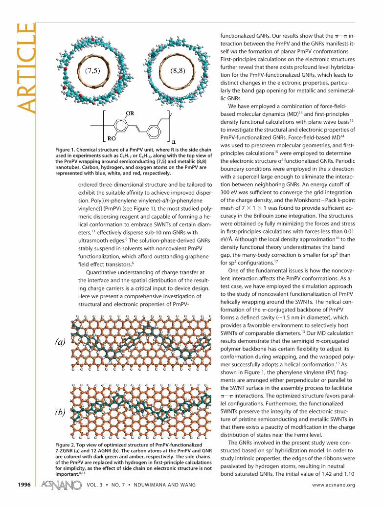
sion. Poly[(m-phenylene vinylene)-alt-(p-phenylene
vinylene)] (PmPV) (see Figure 1), the most studied poly-
meric dispersing reagent and capable of forming a he-
lical conformation to embrace SWNTs of certain diam-
eters,13 effectively disperse sub-10 nm GNRs with
ultrasmooth edges.6 The solution-phase-derived GNRs
stably suspend in solvents with noncovalent PmPV
functionalization, which afford outstanding graphene
field effect transistors.6
Quantitative understanding of charge transfer at
the interface and the spatial distribution of the result-
ing charge carriers is a critical input to device design.
Here we present a comprehensive investigation of
structural and electronic properties of PmPV-
functionalized GNRs. Our results show that the ��� in-teraction between the PmPV and the GNRs manifests it-self via the formation of planar PmPV conformations.First-principles calculations on the electronic structuresfurther reveal that there exists profound level hybridiza-tion for the PmPV-functionalized GNRs, which leads todistinct changes in the electronic properties, particu-larly the band gap opening for metallic and semimetal-lic GNRs.
We have employed a combination of force-field-based molecular dynamics (MD)14 and first-principlesdensity functional calculations with plane wave basis15
to investigate the structural and electronic properties ofPmPV-functionalized GNRs. Force-field-based MD14
was used to prescreen molecular geometries, and first-principles calculations15 were employed to determinethe electronic structure of functionalized GNRs. Periodicboundary conditions were employed in the x directionwith a supercell large enough to eliminate the interac-tion between neighboring GNRs. An energy cutoff of300 eV was sufficient to converge the grid integrationof the charge density, and the Monkhorst�Pack k-pointmesh of 7 � 1 � 1 was found to provide sufficient ac-curacy in the Brillouin zone integration. The structureswere obtained by fully minimizing the forces and stressin first-principles calculations with forces less than 0.01eV/Å. Although the local density approximation16 to thedensity functional theory underestimates the bandgap, the many-body correction is smaller for sp2 thanfor sp3 configurations.17
One of the fundamental issues is how the noncova-lent interaction affects the PmPV conformations. As atest case, we have employed the simulation approachto the study of noncovalent functionalization of PmPVhelically wrapping around the SWNTs. The helical con-formation of the �-conjugated backbone of PmPVforms a defined cavity (�1.5 nm in diameter), whichprovides a favorable environment to selectively hostSWNTs of comparable diameters.13 Our MD calculationresults demonstrate that the semirigid �-conjugatedpolymer backbone has certain flexibility to adjust itsconformation during wrapping, and the wrapped poly-mer successfully adopts a helical conformation.13 Asshown in Figure 1, the phenylene vinylene (PV) frag-ments are arranged either perpendicular or parallel tothe SWNT surface in the assembly process to facilitate��� interactions. The optimized structure favors paral-lel configurations. Furthermore, the functionalizedSWNTs preserve the integrity of the electronic struc-ture of pristine semiconducting and metallic SWNTs inthat there exists a paucity of modification in the chargedistribution of states near the Fermi level.
The GNRs involved in the present study were con-structed based on sp2 hybridization model. In order tostudy intrinsic properties, the edges of the ribbons werepassivated by hydrogen atoms, resulting in neutralbond saturated GNRs. The initial value of 1.42 and 1.10
Figure 1. Chemical structure of a PmPV unit, where R is the side chainused in experiments such as C8H17 or C6H13, along with the top view ofthe PmPV wrapping around semiconducting (7,5) and metallic (8,8)nanotubes. Carbon, hydrogen, and oxygen atoms on the PmPV arerepresented with blue, white, and red, respectively.
Figure 2. Top view of optimized structure of PmPV-functionalized7-ZGNR (a) and 12-AGNR (b). The carbon atoms at the PmPV and GNRare colored with dark green and amber, respectively. The side chainsof the PmPV are replaced with hydrogen in first-principle calculationsfor simplicity, as the effect of side chain on electronic structure is notimportant.6,13
ART
ICLE
VOL. 3 ▪ NO. 7 ▪ NDUWIMANA AND WANG www.acsnano.org1996
Å was used for C�C and C�H bonds, respectively. The
armchair and zigzag structures of GNRs as seen in Fig-
ure 2 were constructed by cutting an infinite graphene
sheet along the (n,n) and (n,0) directions, respectively.
The naming of the armchair and zigzag GNRs (AGNR
and ZGNR) follows the edge structure
nomenclature,10,11 such that an armchair (zigzag) tube
unfolds into a zigzag (armchair) ribbon. Intensive MD
simulation study indicates that the PmPV polymer pos-
sesses flat planar geometries that are spontaneously at-
tracted to the GNRs, in agreement with experimental
observation of a uniform PmPV suspension.6 The ridge
shaped PmPV suspension facilitates planar ��� inter-
actions, which is the counterpart of the helical wrap-
ping pattern on SWNTs. The structures obtained from
force-field-based MD calculations are further fully opti-
mized using the first-principles method. The structural
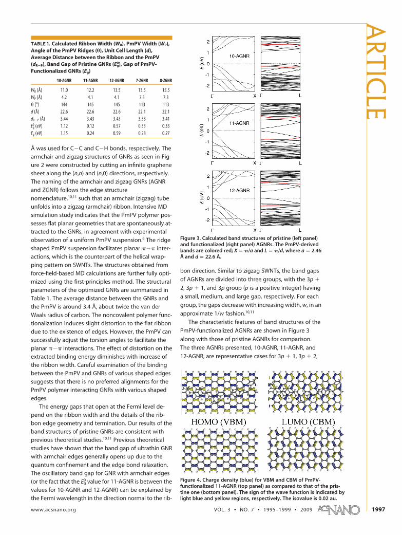
parameters of the optimized GNRs are summarized in
Table 1. The average distance between the GNRs and
the PmPV is around 3.4 Å, about twice the van der
Waals radius of carbon. The noncovalent polymer func-
tionalization induces slight distortion to the flat ribbon
due to the existence of edges. However, the PmPV can
successfully adjust the torsion angles to facilitate the
planar ��� interactions. The effect of distortion on the
extracted binding energy diminishes with increase of
the ribbon width. Careful examination of the binding
between the PmPV and GNRs of various shaped edges
suggests that there is no preferred alignments for the
PmPV polymer interacting GNRs with various shaped
edges.
The energy gaps that open at the Fermi level de-
pend on the ribbon width and the details of the rib-
bon edge geometry and termination. Our results of the
band structures of pristine GNRs are consistent with
previous theoretical studies.10,11 Previous theoretical
studies have shown that the band gap of ultrathin GNR
with armchair edges generally opens up due to the
quantum confinement and the edge bond relaxation.
The oscillatory band gap for GNR with armchair edges
(or the fact that the Eg0 value for 11-AGNR is between the
values for 10-AGNR and 12-AGNR) can be explained by
the Fermi wavelength in the direction normal to the rib-
bon direction. Similar to zigzag SWNTs, the band gaps
of AGNRs are divided into three groups, with the 3p �
2, 3p � 1, and 3p group (p is a positive integer) having
a small, medium, and large gap, respectively. For each
group, the gaps decrease with increasing width, w, in an
approximate 1/w fashion.10,11
The characteristic features of band structures of the
PmPV-functionalized AGNRs are shown in Figure 3
along with those of pristine AGNRs for comparison.
The three AGNRs presented, 10-AGNR, 11-AGNR, and
12-AGNR, are representative cases for 3p � 1, 3p � 2,
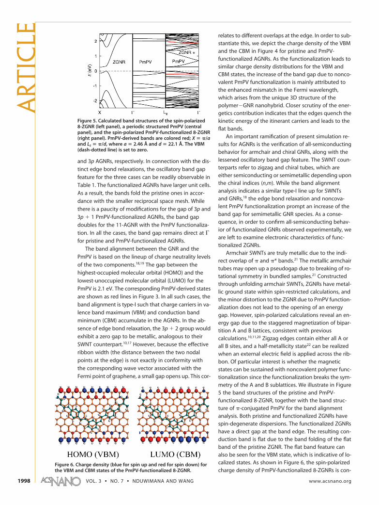
Figure 4. Charge density (blue) for VBM and CBM of PmPV-functionalized 11-AGNR (top panel) as compared to that of the pris-tine one (bottom panel). The sign of the wave function is indicated bylight blue and yellow regions, respectively. The isovalue is 0.02 au.
TABLE 1. Calculated Ribbon Width (WR), PmPV Width (WP),Angle of the PmPV Ridges (�), Unit Cell Length (d),Average Distance between the Ribbon and the PmPV(dR�P), Band Gap of Pristine GNRs (Eg
0), Gap of PmPV-Functionalized GNRs (Eg)
10-AGNR 11-AGNR 12-AGNR 7-ZGNR 8-ZGNR
WR (Å) 11.0 12.2 13.5 13.5 15.5WP (Å) 4.2 4.1 4.1 7.3 7.3� (°) 144 145 145 113 113d (Å) 22.6 22.6 22.6 22.1 22.1dR�P (Å) 3.44 3.43 3.43 3.38 3.41Eg
0 (eV) 1.12 0.12 0.57 0.33 0.33Eg (eV) 1.15 0.24 0.59 0.28 0.27
Figure 3. Calculated band structures of pristine (left panel)and functionalized (right panel) AGNRs. The PmPV-derivedbands are colored red; X � �/a and L � �/d, where a � 2.46Å and d � 22.6 Å.
ARTIC
LE
www.acsnano.org VOL. 3 ▪ NO. 7 ▪ 1995–1999 ▪ 2009 1997
and 3p AGNRs, respectively. In connection with the dis-
tinct edge bond relaxations, the oscillatory band gap
feature for the three cases can be readily observable in
Table 1. The functionalized AGNRs have larger unit cells.
As a result, the bands fold the pristine ones in accor-
dance with the smaller reciprocal space mesh. While
there is a paucity of modifications for the gap of 3p and
3p � 1 PmPV-functionalized AGNRs, the band gap
doubles for the 11-AGNR with the PmPV functionaliza-
tion. In all the cases, the band gap remains direct at �
for pristine and PmPV-functionalized AGNRs.
The band alignment between the GNR and the
PmPV is based on the lineup of charge neutrality levels
of the two components.18,19 The gap between the
highest-occupied molecular orbital (HOMO) and the
lowest-unoccupied molecular orbital (LUMO) for the
PmPV is 2.1 eV. The corresponding PmPV-derived states
are shown as red lines in Figure 3. In all such cases, the
band alignment is type-I such that charge carriers in va-
lence band maximum (VBM) and conduction band
minimum (CBM) accumulate in the AGNRs. In the ab-
sence of edge bond relaxation, the 3p � 2 group would
exhibit a zero gap to be metallic, analogous to their
SWNT counterpart.10,17 However, because the effective
ribbon width (the distance between the two nodal
points at the edge) is not exactly in conformity with
the corresponding wave vector associated with the
Fermi point of graphene, a small gap opens up. This cor-
relates to different overlaps at the edge. In order to sub-stantiate this, we depict the charge density of the VBMand the CBM in Figure 4 for pristine and PmPV-functionalized AGNRs. As the functionalization leads tosimilar charge density distributions for the VBM andCBM states, the increase of the band gap due to nonco-valent PmPV functionalization is mainly attributed tothe enhanced mismatch in the Fermi wavelength,which arises from the unique 3D structure of thepolymer�GNR nanohybrid. Closer scrutiny of the ener-getics contribution indicates that the edges quench thekinetic energy of the itinerant carriers and leads to theflat bands.
An important ramification of present simulation re-sults for AGNRs is the verification of all-semiconductingbehavior for armchair and chiral GNRs, along with thelessened oscillatory band gap feature. The SWNT coun-terparts refer to zigzag and chiral tubes, which areeither semiconducting or semimetallic depending uponthe chiral indices (n,m). While the band alignmentanalysis indicates a similar type-I line up for SWNTsand GNRs,18 the edge bond relaxation and noncova-lent PmPV functionalization prompt an increase of theband gap for semimetallic GNR species. As a conse-quence, in order to confirm all-semiconducting behav-ior of functionalized GNRs observed experimentally, weare left to examine electronic characteristics of func-tionalized ZGNRs.
Armchair SWNTs are truly metallic due to the indi-rect overlap of � and �* bands.21 The metallic armchairtubes may open up a pseudogap due to breaking of ro-tational symmetry in bundled samples.21 Constructedthrough unfolding armchair SWNTs, ZGNRs have metal-lic ground state within spin-restricted calculations, andthe minor distortion to the ZGNR due to PmPV function-alization does not lead to the opening of an energygap. However, spin-polarized calculations reveal an en-ergy gap due to the staggered magnetization of bipar-tition A and B lattices, consistent with previouscalculations.10,11,20 Zigzag edges contain either all A orall B sites, and a half-metallicity state22 can be realizedwhen an external electric field is applied across the rib-bon. Of particular interest is whether the magneticstates can be sustained with noncovalent polymer func-tionalization since the functionalization breaks the sym-metry of the A and B sublattices. We illustrate in Figure5 the band structures of the pristine and PmPV-functionalized 8-ZGNR, together with the band struc-ture of �-conjugated PmPV for the band alignmentanalysis. Both pristine and functionalized ZGNRs havespin-degenerate dispersions. The functionalized ZGNRshave a direct gap at the band edge. The resulting con-duction band is flat due to the band folding of the flatband of the pristine ZGNR. The flat band feature canalso be seen for the VBM state, which is indicative of lo-calized states. As shown in Figure 6, the spin-polarizedcharge density of PmPV-functionalized 8-ZGNRs is con-
Figure 5. Calculated band structures of the spin-polarized8-ZGNR (left panel), a periodic structured PmPV (centralpanel), and the spin-polarized PmPV-functionalized 8-ZGNR(right panel). PmPV-derived bands are colored red; X � �/aand Lz � �/d, where a � 2.46 Å and d � 22.1 Å. The VBM(dash-dotted line) is set to zero.
Figure 6. Charge density (blue for spin up and red for spin down) forthe VBM and CBM states of the PmPV-functionalized 8-ZGNR.
ART
ICLE
VOL. 3 ▪ NO. 7 ▪ NDUWIMANA AND WANG www.acsnano.org1998
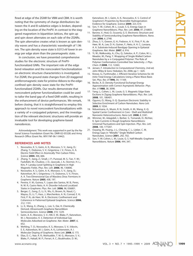
fined at edge of the ZGNR for VBM and CBM. It is worthnoting that the symmetry of charge distributions be-tween the A and B sublattice edges is broken, depend-ing on the location of the PmPV. In contrast to the stag-gered magnetism in bipartition lattices, the spin upand spin down alternates on each side of the ZGNRs.The spin alternative creates what is known as spin den-sity waves and has a characteristic wavelength of 1.96nm. The spin density wave state is 0.013 eV lower in en-ergy per edge atom than the paramagnetic state.
In conclusion, we have presented comprehensivestudies for the electronic structure of PmPV-functionalized GNRs. The important role of the edgebond relaxation and the noncovalent functionalizationon electronic structure characteristics is investigated.For ZGNR, the ground state changes from 2D staggeredantiferromagnetic state for pristine ribbons to the edge-confined spin density wave state for the PmPV-functionalized ZGNRs. Our results demonstrate thatnoncovalent polymer functionalization could be usedto tailor the band gap of a fixed GNR width, resulting inthe enhancement of device performances. We remark,before closing, that it is straightforward to employ thisapproach to novel noncovalent functionalizations witha variety of �-conjugated polymers, and the investiga-tion of the relevant electronic structures will provide aninvaluable tool for developing graphene-basednanodevices.
Acknowledgment. This work was supported in part by the Na-tional Science Foundation (Grant No. DMR-02-05328) and ArmyResearch Office (Grant No. W911NF-06-1-0442).
REFERENCES AND NOTES1. Novoselov, K. S.; Geim, A. K.; Morozov, S. V.; Jiang, D.;
Zhang, Y.; Dubonos, S. V.; Grigorieva, I. V.; Firsov, A. A.Electric Field Effect in Atomically Thin Carbon Films.Science 2004, 306, 666.
2. Zhang, Y.; Jiang, Z.; Small, J. P.; Purewal, M. S.; Tan, Y.-W.;Fazlollahi, M.; Chudow, J. D.; Jaszczak, J. A.; Stormer, H. L.;Kim, P. Landau-Level Splitting in Graphene in HighMagnetic Fields. Phys. Rev. Lett. 2006, 96, 136806.
3. Novoselov, K. S.; Geim, A. K.; Morozov, S. V.; Jiang, D.;Katsnelson, M. I.; Grigorieva, I. V.; Dubonos, S. V.; Firsov,A. A. Two-Dimensional Gas of Massless Dirac Fermions inGraphene. Nature 2005, 438, 197.
4. Pereira, V. M.; Guinea, F.; Lopes dos Santos, M. B.; Peres,N. M. R.; Castro Neto, A. H. Disorder Induced LocalizedStates in Graphene. Phys. Rev. Lett. 2006, 96, 036801.
5. Berger, C.; Song, Z.; Li, X.; Wu, X.; Brown, N.; Naud, C.;Mayou, D.; Li, T.; Hass, J.; Marchenkov, A. N.; Conrad, E. H;First, P. N.; de Heer, W. A. Electronic Confinement andCoherence in Patterned Epitaxial Graphene. Science 2006,312, 1191.
6. Li, X.; Wang, X.; Zhang, L.; Lee, S.; Dai, H. ChemicallyDerived, Ultrasmooth Graphene NanoribbonSemiconductors. Science 2008, 319, 1229.
7. Geim, A. K.; Morozov, S. V.; Hill, E. W.; Blake, P.; Katsnelson,M. I.; Novoselov, K. S. Detection of Individual GasMolecules Adsorbed on Graphene. Nat. Mater. 2007, 6,652.
8. Wehling, T. O.; Novoselov, K. S.; Morozov, S. V.; Vdovin,E. E.; Katsnelson, M. I.; Geim, A. K.; Lichtenstein, A. I.Molecular Doping of Graphene. Nano Lett. 2008, 8, 173.
9. Elias, D. C.; Nair, R. R.; Mohiuddin, T. M. G.; Morozov, S. V.;Blake, P.; Halsall, M. P.; Ferrari, A. C.; Boukhvalov, D. W.;
Katsnelson, M. I.; Geim, A. K.; Novoselov, K. S. Control ofGraphene’s Properties by Reversible Hydrogenation:Evidence for Graphane. Science 2009, 323, 610.
10. Son, Y.-W.; Cohen, M. L.; Louie, S. G. Energy Gaps inGraphene Nanoribbons. Phys. Rev. Lett. 2006, 97, 216803.
11. Barone, V.; Hod, O.; Scuseria, G. E. Electronic Structure andStability of Semiconducting Graphene Nanoribbons. Nano.Lett. 2006, 6, 2748.
12. Zhou, S. Y.; Gweon, G. H.; Fedorov, A. V.; First, P. N.; deHeer, W. A.; Lee, D. H.; Guiner, F.; Neto, A. H. C.; Lanzara,A. A. Substrate-Induced Bandgap Opening in EpitaxialGraphene. Nat. Mater. 2007, 6, 916.
13. Yi, W.; Malkovskiy, A.; Chu, Q.; Sokolov, A. P.; Colon, M. L.;Meador, M.; Pang, Y. Wrapping of Single-Walled CarbonNanotubes by a �-Conjugated Polymer: The Role ofPolymer Conformation-Controlled Size Selectivity. J. Phys.Chem. B 2008, 112, 12263.
14. Jensen, F. Introduction to Computational Chemistry, 2nd ed;John Wiley & Sons: Hoboken, NJ, 2006; pp 1�624.
15. Kresse, G.; Furthmuller, J. Efficient Iterative Schemes for AbInitio Total-Energy Calculations Using a Plane-Wave BasisSet. Phys. Rev. B 1996, 54, 11169.
16. Becke, A. D. Density-Functional Exchange-EnergyApproximation with Correct Asymptotic Behavior. Phys.Rev. A 1988, 38, 3098.
17. Yang, L.; Cohen, L. M.; Louie, G. S. Magnetic Edge-StateExcitons in Zigzag Graphene Nanoribbons. Phys. Rev. Lett.2008, 101, 186401.
18. Ogunro, O.; Wang, X.-Q. Quantum Electronic Stability inSelective Enrichment of Carbon Nanotubes. Nano Lett.2009, 9, 1034.
19. Nduwimana, A.; Musin, R. N.; Smith, A. M.; Wang, X.-Q.Spatial Carrier Confinement in Core�Shell and MultishellNanowire Heterostructures. Nano Lett. 2008, 8, 3341.
20. Wimmer, M.; Adagideli, I.; Berber, S.; Tomanek, D.; Richter,K. Spin Currents in Rough Graphene Nanoribbons:Universal Fluctuations and Spin Injection. Phys. Rev. Lett.2008, 100, 177207.
21. Ouyang, M.; Huang, J.-L.; Cheung, C. L.; Lieber, C. M.Energy Gaps in “Metallic” Single-Walled CarbonNanotubes. Science 2001, 292, 702.
22. Son, Y.-W; Cohen, L. M.; Louie, G. S. Half-Metallic GrapheneNanoribbons. Nature 2006, 444, 347.
ARTIC
LE
www.acsnano.org VOL. 3 ▪ NO. 7 ▪ 1995–1999 ▪ 2009 1999


![7. Supramolecular structures - Acclab h55.it.helsinki.fiknordlun/nanotiede/nanosc7nc.pdf · 7. Supramolecular structures [Poole-Owens 11.5] Supramolecular structures are large molecules](https://img.pdfslide.us/doc/110x75/5f071ded7e708231d41b63bf/7-supramolecular-structures-acclab-h55it-knordlunnanotiedenanosc7ncpdf.jpg)