Embed Size (px)
Citation preview

〇Product structure : Silicon monolithic integrated circuit 〇This product has no designed protection against radioactive rays
.
1/16 TSZ02201-0G3G0C200400-1-2 © 2012 ROHM Co., Ltd. All rights reserved.
10.Dec.2015 Rev.002 TSZ22111 • 14 • 001
www.rohm.com
6-Channel Charge Pump White LED Driver
with 64 Dimming Steps and I2C Compatible Interface BD2606MVV General Description
BD2606MVV is a multi-level brightness control white LED driver that not only ensures efficient boost by automatically changing the boost rate but also works as a constant current driver with 64 steps, so that the driving current can be adjusted finely. This IC is best suited to turn ON white LEDs that require high-accuracy LED brightness control.
Features ■ 6-Ch Parallel LED Driver ■ 64-Step LED Current Adjust Function ■ Inter-LED Relative Current Accuracy: 3% or less ■ LED Individual Lighting/Dimming Control via I2C
BUS Interface ■ Automatic Transition Charge Pump Type DC/DC
Converter (x1, x1.5 and x2) ■ High Efficiency (90% or More at Maximum) ■ Various Protection Functions such as Output
Voltage Protection, Over-Current Limiter and Thermal Shutdown Circuit
Applications This driver is applicable for various fields such as mobile phones, portable game machines and white LED products.
Key Specifications
■ Power Supply Voltage Range: 2.7V to 5.5V ■ Oscillation Frequency: 1.0MHz(Typ) ■ Quiescent Current: 0μA(Typ) ■ Operating Temperature Range: -30°C to +85°C
Package W(Typ) x D(Typ) x H(Max)
Typical Application Circuit
SQFN016V4040 4.00mm x 4.00mm x 1.00mm
GND
LEDA1
LEDA2
LEDB1
LEDB2
EN
SCL
SDA
Battery
IN OUT
C1N
C1P
C2N
C2P
C1 = 1μF
CIN
= 1μF
COUT = 1μF
LEDC1
LEDC2
C2 = 1μF
BD2606MVV
Datasheet
Datasheet

2/16
BD2606MVV
© 2012 ROHM Co., Ltd. All rights reserved. www.rohm.com
TSZ22111・15・001 10.Dec.2015 Rev.002
TSZ02201-0G3G0C200400-1-2
Absolute Maximum Ratings (Ta=25°C)
Parameter Symbol Ratings Unit Condition
Power Supply Voltage VMAX 7 V
Operating Temperature Range Topr -30 to +85 °C
Storage Temperature Range Tstg -55 to +150 °C
Power Dissipation Pd 0.78 (Note 1) W (Note 1) When mounted on a glass epoxy substrate (70mm x 70mm x 1.6mm), derate by 6.2mW/°C for Ta is higher than 25°C. Caution: Operating the IC over the absolute maximum ratings may damage the IC. The damage can either be a short circuit between pins or an open circuit between pins and the internal circuitry. Therefore, it is important to consider circuit protection measures such as adding a fuse, in case the IC is operated over the absolute maximum ratings.
Recommended Operating Conditions (Ta=-30°C to +85°C)
Parameter Symbol Ratings Unit Condition
Operating power supply voltage VCC 2.7 to 5.5 V
Electrical Characteristics (Unless otherwise specified, Ta = 25°C and VIN = 3.6V.)
Parameter Symbol Limit
Unit Conditions Min Typ Max
Quiescent Current IDDQ - 0 7 μA VEN=0V, VIN=3.6V
Circuit Current 1 IDD1 - 1.0 2.6 mA x1 mode, IOUT=0mA, VIN=3,6V
[Charge Pump]
Output Current IOUT - - 120 mA VOUT=4.0V, VIN=3.6V
Oscillation Frequency fOSC 0.8 1.0 1.2 MHz Add=0 x 03, D6=’0’
[LED Driver]
LED Current Absolute Precision ILED-ERR - - ±6.5 % ILED =16.5mA(LEDxCNT=0x20), LED pin voltage 1.0V
LED Current Relative Precision ILED-to-LED - 0.5 ±3.75(Note 2) % ILED =16.5mA(LEDxCNT=0x20) , LED pin voltage 1.0V
LED Control Voltage VLED - 0.2 0.25 V ILEDA1,ILEDA2,ILEDB1, ILEDB2,ILEDC1,ILEDC2
[Logic Interface]
Input ‘L’ Voltage VIL - - 0.4 V EN, SCL, SDA
Input ‘H’ Voltage VIH 1.6 - - V EN, SCL, SDA
Input ‘H’ Current IIH - - 10 μA EN, SCL, SDA=VIN
Input ‘L’ Current IIL -10 - - μA EN, SCL, SDA=GND
‘L’ Level SDA Output VOL - - 0.4 V SDA, 3mA source
- - 0.6 V SDA, 6mA source
[I2C BUS Interface (Standard Mode)]
SCL Clock Frequency fSCLC 0 - 100 kHz
SCL Low Duration tLOW 4.7 - - μs
SCL High Duration tHIGH 4.0 - - μs
Data Hold Time tHD;DAT 0 - 3.45 μs
Data Setup Time tSU;DAT 250 - - ns
Setup Time – Restart Condition tSU;STA 4.7 - - μs
Hold Time – Restart Condition tHD;STA 4.0 - - μs
Setup Time – Stop Condition tSU;STO 4.0 - - μs
Bus Free Time Between Start and Stop
tBUF 4.7 - - μs
[I2C BUS Interface (Fast Mode)]
SCL Clock Frequency fSCL 0 - 400 kHz
SCL Low Duration tLOW 1.3 - - μs
SCL High Duration tHIGH 0.6 - - μs
Data Hold Time tHD;DAT 0 - 0.9 μs
Data Setup Time tSU;DAT 100 - - ns
Setup Time – Restart Condition tSU;STA 0.6 - - μs
Hold Time – Restart Condition tHD;STA 0.6 - - μs
Setup Time – Stop Condition tSU;STO 0.6 - - μs
Bus Free Time Between Start and Stop
tBUF 1.3 - - μs
Interface Startup Time tEN - - 350 μs Bus startup time (after EN=‘H’)
(Note 2) The following expression is used for calculation: ILED-match={(IMAX-IMIN)/(IMAX+IMIN)} x 100 IMAX= Current value in a channel with the maximum current value among all channels IMIN=Current value in a channel with the minimum current value among all channels

3/16
BD2606MVV
© 2012 ROHM Co., Ltd. All rights reserved. www.rohm.com
TSZ22111・15・001 10.Dec.2015 Rev.002
TSZ02201-0G3G0C200400-1-2
Pin Description
Pin
Number
Pin
Name In/Out Function
Pin
Number
Pin
Name In/Out Function
1 LEDA1 Out LED current driver output 9 C2N In/Out Flying capacitor pin negative
(-) side
2 SDA In I2C BUS control pin 10 C2P In/Out Flying capacitor pin positive
(+) side
3 SCL In I2C BUS control pin 11 GND - GND
4 EN In ON/OFF control 12 LEDC2 Out LED current driver output
5 OUT Out Charge pump output 13 LEDC1 Out LED current driver output
6 IN - Power supply 14 LEDB2 Out LED current driver output
7 C1N In/Out Flying capacitor pin negative
(-) side 15 LEDB1 Out LED current driver output
8 C1P In/Out Flying capacitor pin positive
(+) side 16 LEDA2 Out LED current driver output
- Thermal
PAD -
Heat radiation PAD of back
side. Connect to GND - - - -
Block Diagram
Pin number 16pin
×1, ×1.5, ×2 Charge Pump
Over Voltage
Protect
OSC
TSD
I2C I/F
&
Control
Logic
OUT Control
Charge Pump
Mode Control
GND
LEDA1
LEDA2
LEDB1
LEDB2
EN
SCL
SDA
IN OUT
C1N
C1P
C2N
C2P
LEDC2
LEDC2
Current DAC
Current DAC
Current DAC
LEDACNT
LEDBCNT
LEDCCNT
6
6
6

4/16
BD2606MVV
© 2012 ROHM Co., Ltd. All rights reserved. www.rohm.com
TSZ22111・15・001 10.Dec.2015 Rev.002
TSZ02201-0G3G0C200400-1-2
Typical Performance Curves
Ta=25°C
Ta=-30°C
Ta=85°C
Figure 2. Circuit Current 1 vs Input Voltage
(Operation in x1.0 Mode)
Input Voltage: VIN [V]
Cir
cu
it C
urr
ent
1:
I DD
1 [
mA
]
40
50
60
70
80
90
100
2 3 4 5 6 7
Input voltage: Vin[V]
EF
FIC
IEN
CY
[%
]
UP
DOWN
Figure 3. Efficiency Hysteresis vs Input Voltage
(13mA x 6 Lights)
Input Voltage: VIN [V]
Effic
iency [
%]
0
10
20
30
40
50
60
70
80
90
100
2.5 3 3.5 4 4.5 5 5.5 6 6.5 7
Input voltage: Vin[V]
EF
FIC
IEN
CY
[%
]
Ta=85°C
Ta=25°C
Ta=-30°C
Figure 4. Efficiency vs Input Voltage
(3.5mA x 6 Lights)
Input Voltage: VIN [V]
Effic
iency [
%]
0.0
0.4
0.8
1.2
1.6
2.0
2 3 4 5 6 7
Input voltage: Vin[V]
Quie
scent curr
ent: Iq [μ
A]
Ta=-30°C
Ta=25°C Ta=85°C
Figure 1. Quiescent Current vs Input Voltage
(Standby)
Input Voltage: VIN [V]
Qu
iesce
nt
Cu
rre
nt: I
DD
Q[µ
A]

5/16
BD2606MVV
© 2012 ROHM Co., Ltd. All rights reserved. www.rohm.com
TSZ22111・15・001 10.Dec.2015 Rev.002
TSZ02201-0G3G0C200400-1-2
Typical Performance Curves - continued
0
10
20
30
40
50
60
70
80
90
100
2.5 3 3.5 4 4.5 5 5.5 6 6.5 7
Input voltage: Vin[V]
EF
FIC
IEN
CY
[%
]
Ta=25°C
Ta=85°C
Ta=-30°C
Figure 6. Efficiency vs Input Voltage
(20mA x 6 Lights)
Input Voltage: VIN [V]
Effic
iency [
%]
-2.0
-1.5
-1.0
-0.5
0.0
0.5
1.0
1.5
2.0
0 10 20 30 40 50 60
STATE[DEC]
DN
L [LS
B]
Ta=85°C Ta=-30°C
Ta=25°C
Figure 8. LED Current Characteristics
(Differential Linearity Error)
DN
L [
LS
B]
0
10
20
30
40
50
60
70
80
90
100
2.5 3 3.5 4 4.5 5 5.5 6 6.5 7
Input voltage: Vin[V]
EF
FIC
IEN
CY
[%
] Ta=25°C
Ta=85°C
Ta=-30°C
Figure 5. Efficiency vs Input Voltage
(10mA x 6 Lights)
Effic
iency [
%]
Input Voltage: VIN [V]
0.0
2.5
5.0
7.5
10.0
12.5
15.0
17.5
20.0
0.0 0.4 0.8 1.2 1.6 2.0
VLED[V]
LE
D c
urr
ent [m
A]
Ta=25°C
Ta=-30°C
Ta=85°C
Figure 7. LED Current Characteristics vs
LED Control Voltage (LED Current 16.5mA)
LE
D C
urr
en
t [m
A]
LED Control Voltage : VLED [V]

6/16
BD2606MVV
© 2012 ROHM Co., Ltd. All rights reserved. www.rohm.com
TSZ22111・15・001 10.Dec.2015 Rev.002
TSZ02201-0G3G0C200400-1-2
Typical Performance Curves - continued
-2.0
-1.5
-1.0
-0.5
0.0
0.5
1.0
1.5
2.0
0 10 20 30 40 50 60
STATE[DEC]
INL [LS
B]
Ta=85°C Ta=-30°C
Ta=25°C
Figure 9. LED Current Characteristics
(Integral Linearity Error)
INL [
LS
B]
0.0
2.5
5.0
7.5
10.0
12.5
15.0
17.5
20.0
0 1 2 3 4 5 6 7
Input voltage: Vin[V]
LE
D c
urr
ent [m
A]
Ta=25°C
Ta=85°C
Ta=-30°C
Figure 11. LED Current vs Input Voltage
(LED Current 16.5mA)
Input Voltage: VIN [V]
LE
D C
urr
en
t [m
A]
0.0
0.5
1.0
1.5
2.0
2.5
3.0
3.5
4.0
4.5
5.0
0 10 20 30 40 50 60
STATE[DEC]
LE
D c
urr
ent re
lative p
recis
ion [%
]
Ta=-30°C
Ta=25°C
Ta=85°C
Figure 10. LED Current Matching
LE
D C
urr
en
t re
lative
Pre
cis
ion [
%]

7/16
BD2606MVV
© 2012 ROHM Co., Ltd. All rights reserved. www.rohm.com
TSZ22111・15・001 10.Dec.2015 Rev.002
TSZ02201-0G3G0C200400-1-2
SDA
EN
SCL
I2C Interface Buffer
VEN VEN
SDA
SCL
tSU;DAT tLOW
S Sr P S
tBUF
tHD;STA
tSU;STA
tHIGH
tHD;STA
tf
tHD;DAT
tSU;STO
tr
Application Information
1. Description of Operations
(1) LED Driver (a) I2C BUS Interface
BD2606MVV can control the LED ON/OFF, brightness and charge pump switching frequency by writing to the register via the I2C BUS interface. Control by the I2C BUS interface is effective when EN is at ‘H’ level. When EN is at ‘L’ level, this LSI is completely shut down and the control and associated functions via the I2C BUS interface are all stopped. As shown in Figure 12 below, the I2C BUS interface of BD2606MVV operates using the VEN voltage (buffering the EN pin voltage) as supply voltage. For this reason, it is desirable that the ‘H’ voltage in the I2C BUS interface is equal to the EN pin voltage.
Figure 12. I2C BUS Interface Buffer
Figure 13. I2C BUS Interface Timing
BD2606MVV operates as a slave device for the I2C BUS interface.
Slave Address
A7 A6 A5 A4 A3 A2 A1 R/W
1 1 0 0 1 1 0 1/0
Data Format
The data format is shown below. Write format:
S W As As Sr R As As POne-byte register data
7 bit 8 bit 7 bit 8 bit
Slave addressOne-byte register
addressSlave address
Or
S W As As As POne-byte register
addressOne-byte register data
7 bit
Slave address
8 bit 8 bit Read format:
S W As As Sr R As Am POne-byte register
addressSlave address One-byte register dataSlave address
8 bit7 bit 7 bit8 bit (Note) S: Start condition W: ‘0=Write R: ‘1=Read As: Acknowledge (slave -> master) Am: No acknowledge Sr: Repeated start condition P: Stop condition

8/16
BD2606MVV
© 2012 ROHM Co., Ltd. All rights reserved. www.rohm.com
TSZ22111・15・001 10.Dec.2015 Rev.002
TSZ02201-0G3G0C200400-1-2
(b) Register Table Register Map
Address
Hex
Register
name D7 D6 D5 D4 D3 D2 D1 D0 Function
0x00 LEDACNT - - LEDACNT Current setting of ILEDA1/2
0x01 LEDBCNT - - LEDBCNT Current setting of ILEDB1/2
0x02 LEDCCNT - - LEDCCNT Current setting of ILEDC1/2
0x03 LEDPWR
CNT -
FREQNT
1/0 LEDC2 LEDC1 LEDB2 LEDB1 LEDA2 LEDA1
Current driver
ON/OFF control (Note) ‘-’: Invalid at write time
‘-’: ‘L’ at read time Description of Registers
LEDACNT (initial value: undefined) --- <Address: 0x00, Data: [D5: D0]>
LEDBCNT (initial value: undefined) --- <Address: 0x01, Data: [D5: D0]>
LEDCCNT (initial value: undefined) --- <Address: 0x02, Data: [D5: D0]>
LED current values are controlled. LEDA1/A2, LEDB1/B2 and LEDC1/C2 are controlled through the registers
LEDACNT, LEDBCNT and LEDCCNT respectively, and the current setting can be switched every 2 channels.
For the current setting value in each register setting, refer to ‘LED Current Setting Table’ on page 9.
LEDA1 (initial value: ‘0) --- <Address: 0x03, Data: D0>
LEDA2 (initial value: ‘0) --- <Address: 0x03, Data: D1>
LEDB1 (initial value: ‘0) --- <Address: 0x03, Data: D2>
LEDB2 (initial value: ‘0) --- <Address: 0x03, Data: D3>
LEDC1 (initial value: ‘0) --- <Address: 0x03, Data: D4>
LEDC2 (initial value: ‘0) --- <Address: 0x03, Data: D5>
The ON/OFF setting of each LED driver channel is as follows:
’0’: OFF
‘1’ :ON
FREQCNT (initial value: ‘0) --- <Address: 0x03, Data: D6>
The switching frequency of a charge pump is set as follows:
’0’: 1MHz
‘1’: 250kHz
When ‘250kHz’ is selected, the flying capacitor of C1, C2 and COUT must be set to 10µF.
9/16
BD2606MVV
© 2012 ROHM Co., Ltd. All rights reserved. www.rohm.com
TSZ22111・15・001 10.Dec.2015 Rev.002
TSZ02201-0G3G0C200400-1-2
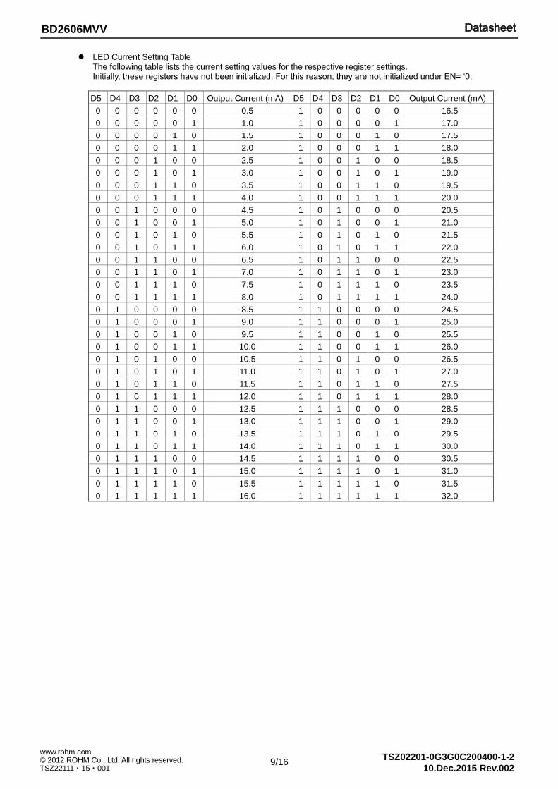
LED Current Setting Table The following table lists the current setting values for the respective register settings. Initially, these registers have not been initialized. For this reason, they are not initialized under EN= ‘0.
D5 D4 D3 D2 D1 D0 Output Current (mA) D5 D4 D3 D2 D1 D0 Output Current (mA)
0 0 0 0 0 0 0.5 1 0 0 0 0 0 16.5
0 0 0 0 0 1 1.0 1 0 0 0 0 1 17.0
0 0 0 0 1 0 1.5 1 0 0 0 1 0 17.5
0 0 0 0 1 1 2.0 1 0 0 0 1 1 18.0
0 0 0 1 0 0 2.5 1 0 0 1 0 0 18.5
0 0 0 1 0 1 3.0 1 0 0 1 0 1 19.0
0 0 0 1 1 0 3.5 1 0 0 1 1 0 19.5
0 0 0 1 1 1 4.0 1 0 0 1 1 1 20.0
0 0 1 0 0 0 4.5 1 0 1 0 0 0 20.5
0 0 1 0 0 1 5.0 1 0 1 0 0 1 21.0
0 0 1 0 1 0 5.5 1 0 1 0 1 0 21.5
0 0 1 0 1 1 6.0 1 0 1 0 1 1 22.0
0 0 1 1 0 0 6.5 1 0 1 1 0 0 22.5
0 0 1 1 0 1 7.0 1 0 1 1 0 1 23.0
0 0 1 1 1 0 7.5 1 0 1 1 1 0 23.5
0 0 1 1 1 1 8.0 1 0 1 1 1 1 24.0
0 1 0 0 0 0 8.5 1 1 0 0 0 0 24.5
0 1 0 0 0 1 9.0 1 1 0 0 0 1 25.0
0 1 0 0 1 0 9.5 1 1 0 0 1 0 25.5
0 1 0 0 1 1 10.0 1 1 0 0 1 1 26.0
0 1 0 1 0 0 10.5 1 1 0 1 0 0 26.5
0 1 0 1 0 1 11.0 1 1 0 1 0 1 27.0
0 1 0 1 1 0 11.5 1 1 0 1 1 0 27.5
0 1 0 1 1 1 12.0 1 1 0 1 1 1 28.0
0 1 1 0 0 0 12.5 1 1 1 0 0 0 28.5
0 1 1 0 0 1 13.0 1 1 1 0 0 1 29.0
0 1 1 0 1 0 13.5 1 1 1 0 1 0 29.5
0 1 1 0 1 1 14.0 1 1 1 0 1 1 30.0
0 1 1 1 0 0 14.5 1 1 1 1 0 0 30.5
0 1 1 1 0 1 15.0 1 1 1 1 0 1 31.0
0 1 1 1 1 0 15.5 1 1 1 1 1 0 31.5
0 1 1 1 1 1 16.0 1 1 1 1 1 1 32.0
10/16
BD2606MVV
© 2012 ROHM Co., Ltd. All rights reserved. www.rohm.com
TSZ22111・15・001 10.Dec.2015 Rev.002
TSZ02201-0G3G0C200400-1-2
(2) Charge Pump (a) Description of Operations
Pin voltage comparison takes place at OUT control section, and then VOUT generation takes place so that the LED cathode voltage with the highest VF is set to 0.1V. A boost rate is changed automatically to a proper one at the Charge Pump Mode Control section so that operation can take place at possible low boost rate. When the current taken from the IN pin exceeds 600mA, the overcurrent limiter is activated and the IC resets. In addition, if the output voltage falls below 1.5V, the IC will reset due to short-circuit at the output.
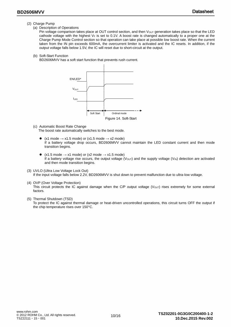
(b) Soft-Start Function
BD2606MVV has a soft start function that prevents rush current.
Soft Start
Ordinal mode
EN/LED*
VOUT
ILED
TOFF
Figure 14. Soft-Start
(c) Automatic Boost Rate Change
The boost rate automatically switches to the best mode.
(x1 mode → x1.5 mode) or (x1.5 mode → x2 mode) If a battery voltage drop occurs, BD2606MVV cannot maintain the LED constant current and then mode transition begins.
(x1.5 mode → x1 mode) or (x2 mode → x1.5 mode) If a battery voltage rise occurs, the output voltage (VOUT) and the supply voltage (VIN) detection are activated and then mode transition begins.
(3) UVLO (Ultra Low Voltage Lock Out)
If the input voltage falls below 2.2V, BD2606MVV is shut down to prevent malfunction due to ultra-low voltage.
(4) OVP (Over Voltage Protection) This circuit protects the IC against damage when the C/P output voltage (VOUT) rises extremely for some external factors.
(5) Thermal Shutdown (TSD)
To protect the IC against thermal damage or heat-driven uncontrolled operations, this circuit turns OFF the output if the chip temperature rises over 150°C.

11/16
BD2606MVV
© 2012 ROHM Co., Ltd. All rights reserved. www.rohm.com
TSZ22111・15・001 10.Dec.2015 Rev.002
TSZ02201-0G3G0C200400-1-2
2. Recommended PCB Layout
In PCB design, wire the power supply line in a way that the PCB impedance goes low and provide a bypass capacitor if needed. Heat radiation of back side PAD is used for improving the efficiency of IC heat radiation. Solder PAD to GND pin. Moreover, connect ground plane of board using via as shown in the patterns of below page. The efficiency of heat radiation improves according to the area of ground plane.
EN OU
T
IN
SCL
To substrate GND
GND SDA
To substrate VCC
CO
UT
CIN
C1
C2
CIN
C1
C2
VCC
CO
UT
OUT
SDA
SCL
Rear-side GND
EN
Figure 15. Application Layout Image (Top View) Figure 16. Front (Top View)
3. Application Parts Selection Method
Capacitor (Use a ceramic capacitor with good frequency and temperature characteristics)
Symbol Recommended Value Recommended Parts Type
COUT,CIN,C1,C2 1μF GRM188B11A105KA61B(MURATA) Ceramic capacitor
Connect an input bypass capacitor CIN between IN and GND pin and an output capacitor between OUT and GND pin in proximity. Place both C1P-C1N and C2P-C2N capacitors in proximity to the chip. Furthermore, select a ceramic capacitor with a sufficient rating for the voltage to be applied.
When other than these parts are used, the equivalent parts must be used.
12/16
BD2606MVV
© 2012 ROHM Co., Ltd. All rights reserved. www.rohm.com
TSZ22111・15・001 10.Dec.2015 Rev.002
TSZ02201-0G3G0C200400-1-2
Operational Notes
1. Reverse Connection of Power Supply
Connecting the power supply in reverse polarity can damage the IC. Take precautions against reverse polarity when connecting the power supply, such as mounting an external diode between the power supply and the IC’s power supply pins.
2. Power Supply Lines
Design the PCB layout pattern to provide low impedance supply lines. Separate the ground and supply lines of the digital and analog blocks to prevent noise in the ground and supply lines of the digital block from affecting the analog block. Furthermore, connect a capacitor to ground at all power supply pins. Consider the effect of temperature and aging on the capacitance value when using electrolytic capacitors.
3. Ground Voltage
Ensure that no pins are at a voltage below that of the ground pin at any time, even during transient condition.
4. Ground Wiring Pattern
When using both small-signal and large-current ground traces, the two ground traces should be routed separately but connected to a single ground at the reference point of the application board to avoid fluctuations in the small-signal ground caused by large currents. Also ensure that the ground traces of external components do not cause variations on the ground voltage. The ground lines must be as short and thick as possible to reduce line impedance.
5. Thermal Consideration
Should by any chance the power dissipation rating be exceeded the rise in temperature of the chip may result in deterioration of the properties of the chip. In case of exceeding this absolute maximum rating, increase the board size and copper area to prevent exceeding the Pd rating.
6. Recommended Operating Conditions
These conditions represent a range within which the expected characteristics of the IC can be approximately obtained. The electrical characteristics are guaranteed under the conditions of each parameter.
7. Inrush Current
When power is first supplied to the IC, it is possible that the internal logic may be unstable and inrush current may flow instantaneously due to the internal powering sequence and delays, especially if the IC has more than one power supply. Therefore, give special consideration to power coupling capacitance, power wiring, width of ground wiring, and routing of connections.
8. Operation Under Strong Electromagnetic Field
Operating the IC in the presence of a strong electromagnetic field may cause the IC to malfunction.
9. Testing on Application Boards
When testing the IC on an application board, connecting a capacitor directly to a low-impedance output pin may subject the IC to stress. Always discharge capacitors completely after each process or step. The IC’s power supply should always be turned off completely before connecting or removing it from the test setup during the inspection process. To prevent damage from static discharge, ground the IC during assembly and use similar precautions during transport and storage.
10. Inter-pin Short and Mounting Errors
Ensure that the direction and position are correct when mounting the IC on the PCB. Incorrect mounting may result in damaging the IC. Avoid nearby pins being shorted to each other especially to ground, power supply and output pin. Inter-pin shorts could be due to many reasons such as metal particles, water droplets (in very humid environment) and unintentional solder bridge deposited in between pins during assembly to name a few.
13/16
BD2606MVV
© 2012 ROHM Co., Ltd. All rights reserved. www.rohm.com
TSZ22111・15・001 10.Dec.2015 Rev.002
TSZ02201-0G3G0C200400-1-2
Operational Notes – continued
11. Unused Input Pins
Input pins of an IC are often connected to the gate of a MOS transistor. The gate has extremely high impedance and extremely low capacitance. If left unconnected, the electric field from the outside can easily charge it. The small charge acquired in this way is enough to produce a significant effect on the conduction through the transistor and cause unexpected operation of the IC. So unless otherwise specified, unused input pins should be connected to the power supply or ground line.
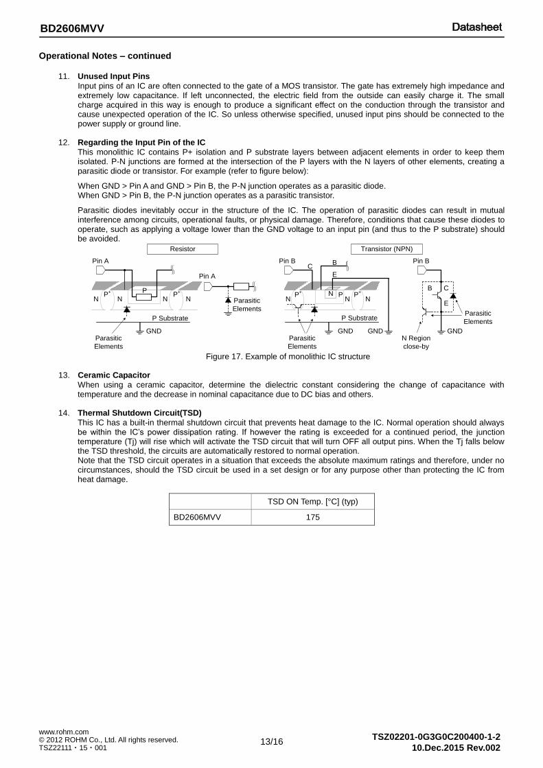
12. Regarding the Input Pin of the IC
This monolithic IC contains P+ isolation and P substrate layers between adjacent elements in order to keep them isolated. P-N junctions are formed at the intersection of the P layers with the N layers of other elements, creating a parasitic diode or transistor. For example (refer to figure below):
When GND > Pin A and GND > Pin B, the P-N junction operates as a parasitic diode. When GND > Pin B, the P-N junction operates as a parasitic transistor.
Parasitic diodes inevitably occur in the structure of the IC. The operation of parasitic diodes can result in mutual interference among circuits, operational faults, or physical damage. Therefore, conditions that cause these diodes to operate, such as applying a voltage lower than the GND voltage to an input pin (and thus to the P substrate) should be avoided.
Figure 17. Example of monolithic IC structure
13. Ceramic Capacitor
When using a ceramic capacitor, determine the dielectric constant considering the change of capacitance with temperature and the decrease in nominal capacitance due to DC bias and others.
14. Thermal Shutdown Circuit(TSD)
This IC has a built-in thermal shutdown circuit that prevents heat damage to the IC. Normal operation should always be within the IC’s power dissipation rating. If however the rating is exceeded for a continued period, the junction temperature (Tj) will rise which will activate the TSD circuit that will turn OFF all output pins. When the Tj falls below the TSD threshold, the circuits are automatically restored to normal operation. Note that the TSD circuit operates in a situation that exceeds the absolute maximum ratings and therefore, under no circumstances, should the TSD circuit be used in a set design or for any purpose other than protecting the IC from heat damage.
TSD ON Temp. [°C] (typ)
BD2606MVV 175
N NP
+ P
N NP
+
P Substrate
GND
NP
+
N NP
+N P
P Substrate
GND GND
Parasitic
Elements
Pin A
Pin A
Pin B Pin B
B C
E
Parasitic
Elements
GNDParasitic
Elements
CB
E
Transistor (NPN)Resistor
N Region
close-by
Parasitic
Elements

14/16
BD2606MVV
© 2012 ROHM Co., Ltd. All rights reserved. www.rohm.com
TSZ22111・15・001 10.Dec.2015 Rev.002
TSZ02201-0G3G0C200400-1-2
Ordering Information
B D 2 6 0 6 M V V - E 2
Part Number
Package
MVV:SQFN016V4040
Packaging and forming specification
E2: Embossed tape and reel
Marking Diagram
SQFN016V4040 (TOP VIEW)
D 2 6 0 6
Part Number Marking
LOT Number
1PIN MARK
15/16
BD2606MVV
© 2012 ROHM Co., Ltd. All rights reserved. www.rohm.com
TSZ22111・15・001 10.Dec.2015 Rev.002
TSZ02201-0G3G0C200400-1-2
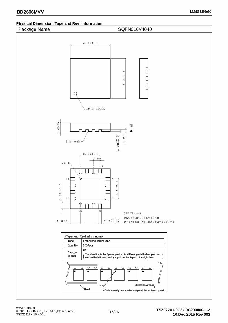
Physical Dimension, Tape and Reel Information
Package Name SQFN016V4040
16/16
BD2606MVV
© 2012 ROHM Co., Ltd. All rights reserved. www.rohm.com
TSZ22111・15・001 10.Dec.2015 Rev.002
TSZ02201-0G3G0C200400-1-2
Revision History
Date Revision Changes
03.Dec.2012 001 New Release
10.Dec.2015 002 Applied the ROHM Standard Style and improved understandability.

DatasheetDatasheet
Notice-PGA-E Rev.002© 2015 ROHM Co., Ltd. All rights reserved.
Notice Precaution on using ROHM Products
1. Our Products are designed and manufactured for application in ordinary electronic equipments (such as AV equipment, OA equipment, telecommunication equipment, home electronic appliances, amusement equipment, etc.). If you intend to use our Products in devices requiring extremely high reliability (such as medical equipment (Note 1), transport equipment, traffic equipment, aircraft/spacecraft, nuclear power controllers, fuel controllers, car equipment including car accessories, safety devices, etc.) and whose malfunction or failure may cause loss of human life, bodily injury or serious damage to property (“Specific Applications”), please consult with the ROHM sales representative in advance. Unless otherwise agreed in writing by ROHM in advance, ROHM shall not be in any way responsible or liable for any damages, expenses or losses incurred by you or third parties arising from the use of any ROHM’s Products for Specific Applications.
(Note1) Medical Equipment Classification of the Specific Applications JAPAN USA EU CHINA
CLASSⅢ CLASSⅢ
CLASSⅡb CLASSⅢ
CLASSⅣ CLASSⅢ
2. ROHM designs and manufactures its Products subject to strict quality control system. However, semiconductor
products can fail or malfunction at a certain rate. Please be sure to implement, at your own responsibilities, adequate safety measures including but not limited to fail-safe design against the physical injury, damage to any property, which a failure or malfunction of our Products may cause. The following are examples of safety measures:
[a] Installation of protection circuits or other protective devices to improve system safety [b] Installation of redundant circuits to reduce the impact of single or multiple circuit failure
3. Our Products are designed and manufactured for use under standard conditions and not under any special or extraordinary environments or conditions, as exemplified below. Accordingly, ROHM shall not be in any way responsible or liable for any damages, expenses or losses arising from the use of any ROHM’s Products under any special or extraordinary environments or conditions. If you intend to use our Products under any special or extraordinary environments or conditions (as exemplified below), your independent verification and confirmation of product performance, reliability, etc, prior to use, must be necessary:
[a] Use of our Products in any types of liquid, including water, oils, chemicals, and organic solvents [b] Use of our Products outdoors or in places where the Products are exposed to direct sunlight or dust [c] Use of our Products in places where the Products are exposed to sea wind or corrosive gases, including Cl2,
H2S, NH3, SO2, and NO2
[d] Use of our Products in places where the Products are exposed to static electricity or electromagnetic waves [e] Use of our Products in proximity to heat-producing components, plastic cords, or other flammable items [f] Sealing or coating our Products with resin or other coating materials [g] Use of our Products without cleaning residue of flux (even if you use no-clean type fluxes, cleaning residue of
flux is recommended); or Washing our Products by using water or water-soluble cleaning agents for cleaning residue after soldering
[h] Use of the Products in places subject to dew condensation
4. The Products are not subject to radiation-proof design. 5. Please verify and confirm characteristics of the final or mounted products in using the Products. 6. In particular, if a transient load (a large amount of load applied in a short period of time, such as pulse. is applied,
confirmation of performance characteristics after on-board mounting is strongly recommended. Avoid applying power exceeding normal rated power; exceeding the power rating under steady-state loading condition may negatively affect product performance and reliability.
7. De-rate Power Dissipation depending on ambient temperature. When used in sealed area, confirm that it is the use in
the range that does not exceed the maximum junction temperature. 8. Confirm that operation temperature is within the specified range described in the product specification. 9. ROHM shall not be in any way responsible or liable for failure induced under deviant condition from what is defined in
this document.
Precaution for Mounting / Circuit board design 1. When a highly active halogenous (chlorine, bromine, etc.) flux is used, the residue of flux may negatively affect product
performance and reliability.
2. In principle, the reflow soldering method must be used on a surface-mount products, the flow soldering method must be used on a through hole mount products. If the flow soldering method is preferred on a surface-mount products, please consult with the ROHM representative in advance.
For details, please refer to ROHM Mounting specification

DatasheetDatasheet
Notice-PGA-E Rev.002© 2015 ROHM Co., Ltd. All rights reserved.
Precautions Regarding Application Examples and External Circuits 1. If change is made to the constant of an external circuit, please allow a sufficient margin considering variations of the
characteristics of the Products and external components, including transient characteristics, as well as static characteristics.
2. You agree that application notes, reference designs, and associated data and information contained in this document
are presented only as guidance for Products use. Therefore, in case you use such information, you are solely responsible for it and you must exercise your own independent verification and judgment in the use of such information contained in this document. ROHM shall not be in any way responsible or liable for any damages, expenses or losses incurred by you or third parties arising from the use of such information.
Precaution for Electrostatic
This Product is electrostatic sensitive product, which may be damaged due to electrostatic discharge. Please take proper caution in your manufacturing process and storage so that voltage exceeding the Products maximum rating will not be applied to Products. Please take special care under dry condition (e.g. Grounding of human body / equipment / solder iron, isolation from charged objects, setting of Ionizer, friction prevention and temperature / humidity control).
Precaution for Storage / Transportation 1. Product performance and soldered connections may deteriorate if the Products are stored in the places where:
[a] the Products are exposed to sea winds or corrosive gases, including Cl2, H2S, NH3, SO2, and NO2 [b] the temperature or humidity exceeds those recommended by ROHM [c] the Products are exposed to direct sunshine or condensation [d] the Products are exposed to high Electrostatic
2. Even under ROHM recommended storage condition, solderability of products out of recommended storage time period may be degraded. It is strongly recommended to confirm solderability before using Products of which storage time is exceeding the recommended storage time period.
3. Store / transport cartons in the correct direction, which is indicated on a carton with a symbol. Otherwise bent leads
may occur due to excessive stress applied when dropping of a carton. 4. Use Products within the specified time after opening a humidity barrier bag. Baking is required before using Products of
which storage time is exceeding the recommended storage time period.
Precaution for Product Label QR code printed on ROHM Products label is for ROHM’s internal use only.
Precaution for Disposition When disposing Products please dispose them properly using an authorized industry waste company.
Precaution for Foreign Exchange and Foreign Trade act Since concerned goods might be fallen under listed items of export control prescribed by Foreign exchange and Foreign trade act, please consult with ROHM in case of export.
Precaution Regarding Intellectual Property Rights 1. All information and data including but not limited to application example contained in this document is for reference
only. ROHM does not warrant that foregoing information or data will not infringe any intellectual property rights or any other rights of any third party regarding such information or data.
2. ROHM shall not have any obligations where the claims, actions or demands arising from the combination of the Products with other articles such as components, circuits, systems or external equipment (including software).
3. No license, expressly or implied, is granted hereby under any intellectual property rights or other rights of ROHM or any third parties with respect to the Products or the information contained in this document. Provided, however, that ROHM will not assert its intellectual property rights or other rights against you or your customers to the extent necessary to manufacture or sell products containing the Products, subject to the terms and conditions herein.
Other Precaution 1. This document may not be reprinted or reproduced, in whole or in part, without prior written consent of ROHM.
2. The Products may not be disassembled, converted, modified, reproduced or otherwise changed without prior written consent of ROHM.
3. In no event shall you use in any way whatsoever the Products and the related technical information contained in the Products or this document for any military purposes, including but not limited to, the development of mass-destruction weapons.
4. The proper names of companies or products described in this document are trademarks or registered trademarks of ROHM, its affiliated companies or third parties.

DatasheetDatasheet
Notice – WE Rev.001© 2015 ROHM Co., Ltd. All rights reserved.
General Precaution 1. Before you use our Pro ducts, you are requested to care fully read this document and fully understand its contents.
ROHM shall n ot be in an y way responsible or liabl e for fa ilure, malfunction or acci dent arising from the use of a ny ROHM’s Products against warning, caution or note contained in this document.
2. All information contained in this docume nt is current as of the issuing date and subj ect to change without any prior
notice. Before purchasing or using ROHM’s Products, please confirm the la test information with a ROHM sale s representative.
3. The information contained in this doc ument is provi ded on an “as is” basis and ROHM does not warrant that all
information contained in this document is accurate an d/or error-free. ROHM shall not be in an y way responsible or liable for any damages, expenses or losses incurred by you or third parties resulting from inaccuracy or errors of or concerning such information.