Embed Size (px)
Citation preview

Freescale SemiconductorApplication Note
Document Number: AN3743Rev. 0, 10/2008
Contents
Introduction . . . . . . . . . . . . . . . . . . . . . . . . . . . . . . . . . . . 11.1 Emulated EEPROM. . . . . . . . . . . . . . . . . . . . . . . . . 11.2 Objective . . . . . . . . . . . . . . . . . . . . . . . . . . . . . . . . . 1S12XE EEE in the S12X Memory Map . . . . . . . . . . . . . . 2Configurations of the Enhanced EEPROM Region . . . . . 3
3.1 Launching FTM Commands . . . . . . . . . . . . . . . . . . 43.2 Checking for Errors . . . . . . . . . . . . . . . . . . . . . . . . . 6EEEPROM Quick Start Project Setup . . . . . . . . . . . . . . . 7Accessing EEPROM . . . . . . . . . . . . . . . . . . . . . . . . . . . 10EEE Quick Start Code Steps. . . . . . . . . . . . . . . . . . . . . 12Summary . . . . . . . . . . . . . . . . . . . . . . . . . . . . . . . . . . . . 18
Emulated EEPROM Quick Start Guideby: Matthew Grant
16-Bit ApplicationsFreescale Semiconductor
1 Introduction
1.1 Emulated EEPROMSome families of the S12X series of microcontrollers (MCUs), such as the MC9S12XEP100, have an enhanced region labeled as EEPROM in the memory map. This region does not contain conventional EEPROM, but has flash and RAM components that can be managed by the enhanced flash module (FTM) in a unique manner, allowing the emulation of EEPROM. Because the FTM allows the partitioning of EEPROM resources to suit an application, a significant degree of memory flexibility becomes available to users.
1.2 ObjectiveThe objective of this application note is to accelerate the introduction of emulated EEPROM (EEE). In particular, it is suited to individuals familiar with programming and the use of a debugger but who have little or no experience
1
23
4567
© Freescale Semiconductor, Inc., 2008. All rights reserved.
S12XE EEE in the S12X Memory Map
with EEE. This document seeks to teach users through a simple EEE example. Most low-level details are put aside so as to allow focus on higher-level concepts associated with the EEE. Users will need a programming board with an S12XE MCU and a debugger to single-step through the example code and run through portions of that code. This document shows:
• Where the EEE components exist in the memory map• Examples of three configurations• The FTM command flow• How data behaves in the buffer RAM in different configurations
Other important topics are also discussed. For more details on EEE, refer to Freescale application note AN3490, “Overview of the MC9S12XE Emulated EEPROM,” available at www.freescale.com.
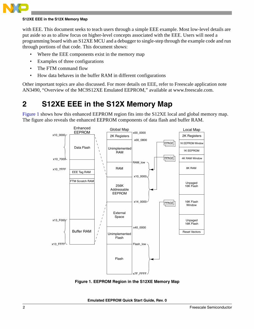
2 S12XE EEE in the S12X Memory MapFigure 1 shows how this enhanced EEPROM region fits into the S12XE local and global memory map. The figure also reveals the enhanced EEPROM components of data flash and buffer RAM.
Figure 1. EEPROM Region in the S12XE Memory Map
Buffer RAM
FTM Scratch RAM
External
Data Flash
EnhancedEEPROM
EEE Tag RAM
UnimplementedRAM
256KAddressable
EEPROM
Space
UnimplementedFlash
Flash
Global Map
RAM
2K Registers
PPAGE
EPAGE
RPAGE
2K Registers
1K EEPROM Window
1K EEPROM
4K RAM Window
8K RAM
Unpaged16K Flash
16K FlashWindow
Unpaged16K Flash
Reset Vectors
Local Mapx10_0000
x13_F000
x10_7000
x10_7FFF
x13_FFFF
x00_0000
x00_0800
RAM_low
x10_0000
x14_0000
x40_0000
x7F_FFFF
Flash_low
Emulated EEPROM Quick Start Guide, Rev. 0
Freescale Semiconductor2
Configurations of the Enhanced EEPROM Region
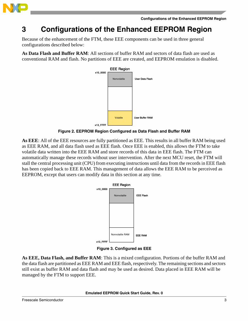
3 Configurations of the Enhanced EEPROM RegionBecause of the enhancement of the FTM, these EEE components can be used in three general configurations described below:
As Data Flash and Buffer RAM: All sections of buffer RAM and sectors of data flash are used as conventional RAM and flash. No partitions of EEE are created, and EEPROM emulation is disabled.
Figure 2. EEPROM Region Configured as Data Flash and Buffer RAM
As EEE: All of the EEE resources are fully partitioned as EEE. This results in all buffer RAM being used as EEE RAM, and all data flash used as EEE flash. Once EEE is enabled, this allows the FTM to take volatile data written into the EEE RAM and store records of this data in EEE flash. The FTM can automatically manage these records without user intervention. After the next MCU reset, the FTM will stall the central processing unit (CPU) from executing instructions until data from the records in EEE flash has been copied back to EEE RAM. This management of data allows the EEE RAM to be perceived as EEPROM, except that users can modify data in this section at any time.
Figure 3. Configured as EEE
As EEE, Data Flash, and Buffer RAM: This is a mixed configuration. Portions of the buffer RAM and the data flash are partitioned as EEE RAM and EEE flash, respectively. The remaining sections and sectors still exist as buffer RAM and data flash and may be used as desired. Data placed in EEE RAM will be managed by the FTM to support EEE.
User Data Flash
User Buffer RAM
Nonvolatile
Volatile
EEE Region
x13_FFFF
x10_0000
User Data Flash
User Buffer RAM
Nonvolatile
Volatile
EEE Region
x13_FFFF
x10_0000
EEE Flash
EEE RAM
Nonvolatile
Nonvolatile RAM
EEE Region
x13_FFFF
x10_0000
EEE Flash
EEE RAM
Nonvolatile
Nonvolatile RAM
EEE Region
x13_FFFF
x10_0000
Emulated EEPROM Quick Start Guide, Rev. 0
Freescale Semiconductor 3

Configurations of the Enhanced EEPROM Region
Figure 4. Configured as EEE, Data Flash, and Buffer RAM
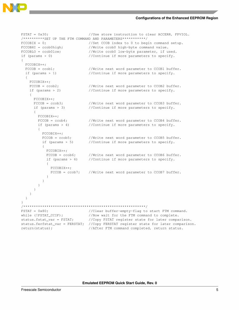
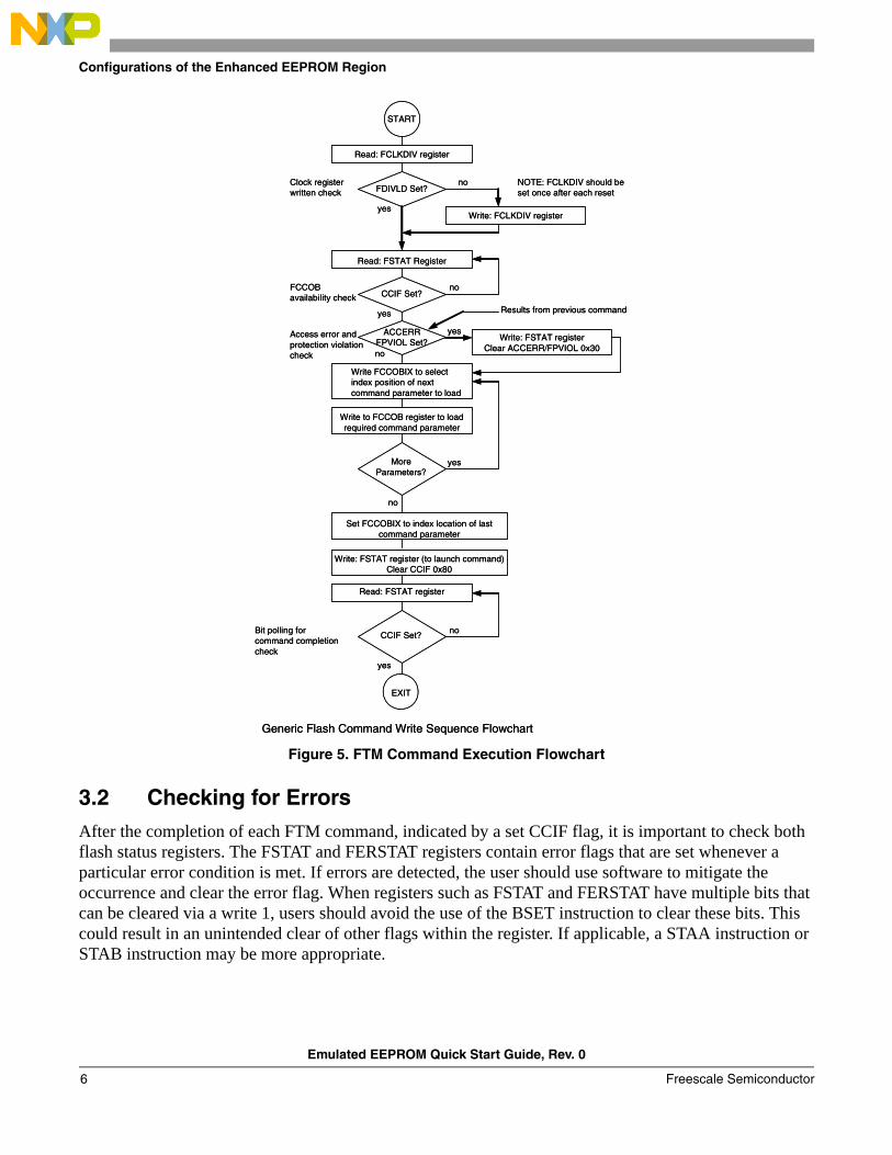
3.1 Launching FTM CommandsIn order to write, read, or configure the memory regions associated with the FTM, commands must be loaded into the FTM and executed. The process involves a specific sequence that is used to set the FTM command parameters and launch execution. The following portion of code illustrates an example of instructions within a function, “LaunchFlashCommand,” used to set up and execute FTM commands. Users should follow a defined flow to reduce the risk of module errors. Figure 5 shows the recommended FTM command execution flow.
User Data Flash
EEE Flash
User Buffer RAM
EEE RAM
Nonvolatile
Nonvolatile
Volatile
Nonvolatile RAM
EEE Region
x13_FFFF
x10_0000
User Data Flash
EEE Flash
User Buffer RAM
EEE RAM
Nonvolatile
Nonvolatile
Volatile
Nonvolatile RAM
EEE Region
x13_FFFF
x10_0000
Emulated EEPROM Quick Start Guide, Rev. 0
Freescale Semiconductor4
Configurations of the Enhanced EEPROM Region
FSTAT = 0x30; //Use store instruction to clear ACCERR, FPVIOL./**********SET UP THE FTM COMMAND AND PARAMETERS***********/FCCOBIX = 0; //Set CCOB index to 0 to begin command setup.FCCOBHI = ccob0high; //Write ccob0 high-byte command value.FCCOBLO = ccob0low; //Write ccob0 low-byte parameter, if used.if (params > 0) //Continue if more parameters to specify.{
FCCOBIX++;FCCOB = ccob1; //Write next word parameter to CCOB1 buffer.if (params > 1) //Continue if more parameters to specify.{FCCOBIX++;FCCOB = ccob2; //Write next word parameter to CCOB2 buffer.if (params > 2) //Continue if more parameters to specify.{
FCCOBIX++;FCCOB = ccob3; //Write next word parameter to CCOB3 buffer.if (params > 3) //Continue if more parameters to specify.{
FCCOBIX++;FCCOB = ccob4; //Write next word parameter to CCOB4 buffer.if (params > 4) //Continue if more parameters to specify.{
FCCOBIX++;FCCOB = ccob5; //Write next word parameter to CCOB5 buffer.if (params > 5) //Continue if more parameters to specify.{FCCOBIX++;FCCOB = ccob6; //Write next word parameter to CCOB6 buffer.if (params > 6) //Continue if more parameters to specify.{
FCCOBIX++;FCCOB = ccob7; //Write next word parameter to CCOB7 buffer.
}}
}}
}}
}/**********************************************************/FSTAT = 0x80; //Clear buffer-empty-flag to start FTM command.while (!FSTAT_CCIF); //Now wait for the FTM command to complete.status.fstat_var = FSTAT; //Copy FSTAT register state for later comparison.status.ferfstat_var = FERSTAT; //Copy FERSTAT register state for later comparison.return(status); //After FTM command completed, return status.
Emulated EEPROM Quick Start Guide, Rev. 0
Freescale Semiconductor 5
Configurations of the Enhanced EEPROM Region
Figure 5. FTM Command Execution Flowchart
3.2 Checking for ErrorsAfter the completion of each FTM command, indicated by a set CCIF flag, it is important to check both flash status registers. The FSTAT and FERSTAT registers contain error flags that are set whenever a particular error condition is met. If errors are detected, the user should use software to mitigate the occurrence and clear the error flag. When registers such as FSTAT and FERSTAT have multiple bits that can be cleared via a write 1, users should avoid the use of the BSET instruction to clear these bits. This could result in an unintended clear of other flags within the register. If applicable, a STAA instruction or STAB instruction may be more appropriate.
ACCERR FPVIOL Set?
START
Read: FCLKDIV register
FDIVLD Set?
Read: FSTAT Register
Write: FCLKDIV register
Write FCCOBIX to select index position of next command parameter to load
Write to FCCOB register to load required command parameter
More Parameters?
Write: FSTAT register (to launch command) Clear CCIF 0x80
Read: FSTAT register
CCIF Set?
EXIT
CCIF Set?
Results from previous command
Write: FSTAT register Clear ACCERR/FPVIOL 0x30
no
yes
no
yes
no
yes
yes
no
no
yes
NOTE: FCLKDIV should be set once after each reset
Clock register written check
FCCOB availability check
Access error and protection violation check
Bit polling for command completion check
Generic Flash Command Write Sequence Flowchart
Set FCCOBIX to index location of last command parameter
Emulated EEPROM Quick Start Guide, Rev. 0
Freescale Semiconductor6

EEEPROM Quick Start Project Setup
4 EEEPROM Quick Start Project SetupThe EEEPROM Quick Start project containing the example code for this application note can be downloaded from the Freescale public website. Users without a compiler can also download a free version of CodeWarrior™ for the S12X. To begin setup of the EEEPROM Quick Start project, open the “EEEPROM_Quick_Start.mcp” project file. Once opened, users should select and open the “main.c” file, which contains the majority of the code referenced in this application note. Comments have been placed throughout the file, along with step numbers that correspond with the discussion in this application note.
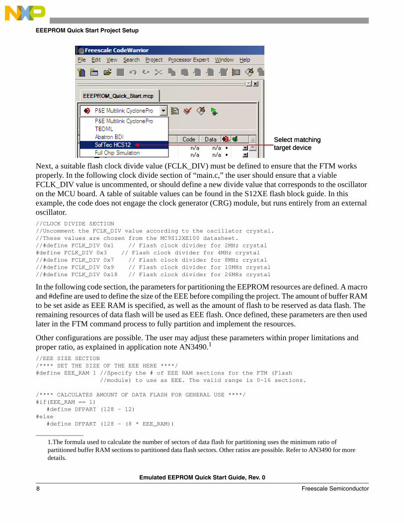
Before attempting to compile and load the project, a few important settings must be checked. First, a target should be selected that matches the communication device that the user will use when programming the MCU.
Open the main.c fileOpen the main.c file
Emulated EEPROM Quick Start Guide, Rev. 0
Freescale Semiconductor 7
EEEPROM Quick Start Project Setup
Next, a suitable flash clock divide value (FCLK_DIV) must be defined to ensure that the FTM works properly. In the following clock divide section of “main.c,” the user should ensure that a viable FCLK_DIV value is uncommented, or should define a new divide value that corresponds to the oscillator on the MCU board. A table of suitable values can be found in the S12XE flash block guide. In this example, the code does not engage the clock generator (CRG) module, but runs entirely from an external oscillator.//CLOCK DIVIDE SECTION//Uncomment the FCLK_DIV value according to the oscillator crystal.//These values are chosen from the MC9S12XE100 datasheet.//#define FCLK_DIV 0x1 // Flash clock divider for 2MHz crystal#define FCLK_DIV 0x3 // Flash clock divider for 4MHz crystal//#define FCLK_DIV 0x7 // Flash clock divider for 8MHz crystal//#define FCLK_DIV 0x9 // Flash clock divider for 10MHz crystal//#define FCLK_DIV 0x18 // Flash clock divider for 26MHz crystal
In the following code section, the parameters for partitioning the EEPROM resources are defined. A macro and #define are used to define the size of the EEE before compiling the project. The amount of buffer RAM to be set aside as EEE RAM is specified, as well as the amount of flash to be reserved as data flash. The remaining resources of data flash will be used as EEE flash. Once defined, these parameters are then used later in the FTM command process to fully partition and implement the resources.
Other configurations are possible. The user may adjust these parameters within proper limitations and proper ratio, as explained in application note AN3490.1
//EEE SIZE SECTION/**** SET THE SIZE OF THE EEE HERE ****/#define EEE_RAM 1 //Specify the # of EEE RAM sections for the FTM (Flash //module) to use as EEE. The valid range is 0-16 sections.
/**** CALCULATES AMOUNT OF DATA FLASH FOR GENERAL USE ****/#if(EEE_RAM == 1) #define DFPART (128 - 12)#else #define DFPART (128 - (8 * EEE_RAM))
1.The formula used to calculate the number of sectors of data flash for partitioning uses the minimum ratio of partitioned buffer RAM sections to partitioned data flash sectors. Other ratios are possible. Refer to AN3490 for more details.
Select matching target deviceSelect matching target device
Emulated EEPROM Quick Start Guide, Rev. 0
Freescale Semiconductor8
EEEPROM Quick Start Project Setup
#endif
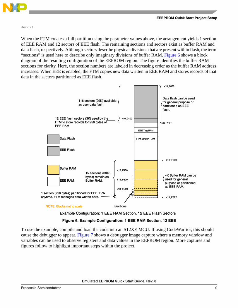
When the FTM creates a full partition using the parameter values above, the arrangement yields 1 section of EEE RAM and 12 sectors of EEE flash. The remaining sections and sectors exist as buffer RAM and data flash, respectively. Although sectors describe physical divisions that are present within flash, the term “sections” is used here to describe only imaginary divisions of buffer RAM. Figure 6 shows a block diagram of the resulting configuration of the EEPROM region. The figure identifies the buffer RAM sections for clarity. Here, the section numbers are labeled in decreasing order as the buffer RAM address increases. When EEE is enabled, the FTM copies new data written in EEE RAM and stores records of that data in the sectors partitioned as EEE flash.
Figure 6. Example Configuration: 1 EEE RAM Section, 12 EEE
To use the example, compile and load the code into an S12XE MCU. If using CodeWarrior, this should cause the debugger to appear. Figure 7 shows a debugger image capture where a memory window and variables can be used to observe registers and data values in the EEPROM region. More captures and figures follow to highlight important steps within the project.
EEE Tag RAM
FTM scratch RAM
x13_FFFF
x13_F000
x10_0000
x10_7FFF
x13_F400
x13_F800
x13_FC00
4K Buffer RAM can be used for general purpose or partitioned as EEE RAM.
Data flash can be used for general purpose or partitioned as EEE flash.
15 sections (3840 bytes) remain as Buffer RAM.
1 section (256 bytes) partitioned for EEE. R/W anytime. FTM manages data written here.
12 EEE flash sectors (3K) used by the FTM to store records for 256 bytes of EEE RAM
116 sectors (29K) available as user data flash
x10_7400
1234
.
.
.
Sections
EEE RAM
Buffer RAM
Data Flash
EEE Flash
Example Configuration: 1 EEE RAM Section, 12 EEE Flash Sectors
NOTE: Blocks not to scale
Emulated EEPROM Quick Start Guide, Rev. 0
Freescale Semiconductor 9

Accessing EEPROM
Figure 7. Debugger Example
5 Accessing EEPROMTo read and write within the EEPROM region, pointers can be assigned appropriate address locations. This is done at the beginning of the main function, as shown in the code below and in Figure 8. At different stages of the programming example, text strings will be written into adjacent sections 1 and 2 of EEE RAM and buffer RAM, respectively. In this case, adjacent sections are chosen to make the difference in behavior more apparent in the memory window. As users proceed, the behavior of the text strings should be observed after each example step. This will help users understand the emulated properties of EEE RAM versus general buffer RAM.
Emulated EEPROM Quick Start Guide, Rev. 0
Freescale Semiconductor10

Accessing EEPROM
/******************************************************************************/void main(void){volatile char before[]="BEFORE"; //Chars to be written to the EEE and Buffer RAMvolatile char during[]=" DURING";//Chars to be written to the EEE and Buffer RAMvolatile char after[]=" AFTER"; //Chars to be written to the EEE and Buffer RAMsigned char dfPart, erPart; //Holds EEE partition size of data Flash and buffer RAMchar * section1_ptr; //Points to location within section1 of buffer RAMchar * section2_ptr; //Points to location within section2 of buffer RAMvolatile ErrType status;
EnableInterrupts; section1_ptr = (signed char *) 0x0F00;//Assign beginning address of section1 of //EEE RAM to pointer. section2_ptr = (signed char *) 0x0E00;//Assign beginning address of section2 of //buffer RAM to pointer.
Figure 8. Assigning Address Locations to Pointers
Beginning address of sections 1 and 2.pointer assigned beginning of
section address in C code
Beginning address of sections 1 and 2.pointer assigned beginning of
section address in C code
Emulated EEPROM Quick Start Guide, Rev. 0
Freescale Semiconductor 11

EEE Quick Start Code Steps
6 EEE Quick Start Code StepsThe remainder of this application note proceeds through ten steps labeled in the main project function. Each step is followed by a corresponding image capture of the code. Users should use a debugger to execute the code and observe the changes that occur in the debugger memory window. This should help to understand some of the EEE behavior.
1. Assign the previously defined FCLK_DIV value to the flash clock divide register (FCLKDIV). This is necessary before any commands can be issued to the FTM.
/*********(1)SET UP THE FLASH CLOCK DIVIDE REGISTER********/while (!FSTAT_CCIF) //Wait for FTM to be ready{}FCLKDIV = FCLK_DIV; //Now write FCLKDIV before using the FTM.if(FCLKDIV != (FCLK_DIV | 0x80)) //Ensure the value is written.
ReportError(FDIV_NOT_SET); //Report an error code./**********************************************************/
2. Use the debugger memory window to see the contents of sections 1 and 2 of the EEE RAM and buffer RAM respectively, before any data is modified.
/****(2)CHECK BUFFER RAM CONTENTS FROM THE PREVIOUS RUN****///Before any FTM commands are executed, check the debugger memory//window and observe the contents of sections 1 (0xF00 to 0xFFF)//and 2 (0xE00 to 0xEFF) of the buffer RAM./**********************************************************/
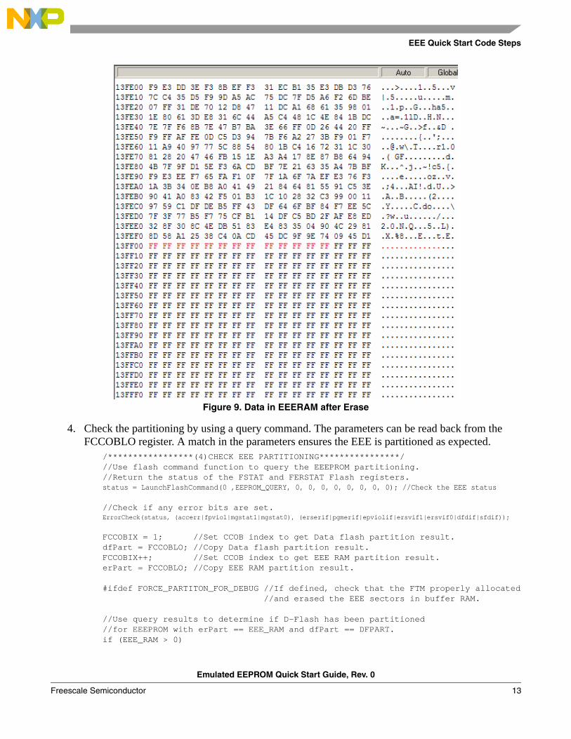
3. The “LaunchFlashCommand” function was written in this application note to accept parameters and execute FTM commands. For this step, a full partition is performed, which erases and initializes EEE RAM and EEE flash. Afterwards, the debugger memory window (Figure 9) shows all data in EEE RAM (section 1) in an erased state (0xFFFF). Adjacent sections of buffer RAM not managed by the FTM have seemingly random data values. Users should always check the FSTAT and FERSTAT registers for errors after completion of an FTM command.
/***********(3)PERFORM FULL PARTITION OF EEE RAM***********/#ifdef FORCE_PARTITON_FOR_DEBUG //If defined, force EEE partition and eraser.
//Run LaunchFlashCommand to partition and erase the EEE in debug mode. //Return the status of the FSTAT and FERSTAT Flash registers. status = LaunchFlashCommand(2 ,FULL_PARTITION_D_FLASH, 0, DFPART, EEE_RAM, 0, 0, 0, 0, 0); //Always check if any error bits are set. ErrorCheck(status, accerr|fpviol|mgstat1|mgstat0, erserif|pgmerif|epviolif|ersvif1|ersvif0|dfdif|sfdif);#endif /**********************************************************/
Emulated EEPROM Quick Start Guide, Rev. 0
Freescale Semiconductor12
EEE Quick Start Code Steps
Figure 9. Data in EEERAM after Erase
4. Check the partitioning by using a query command. The parameters can be read back from the FCCOBLO register. A match in the parameters ensures the EEE is partitioned as expected.
/*****************(4)CHECK EEE PARTITIONING****************///Use flash command function to query the EEEPROM partitioning.//Return the status of the FSTAT and FERSTAT Flash registers.status = LaunchFlashCommand(0 ,EEPROM_QUERY, 0, 0, 0, 0, 0, 0, 0, 0); //Check the EEE status
//Check if any error bits are set.ErrorCheck(status, (accerr|fpviol|mgstat1|mgstat0), (erserif|pgmerif|epviolif|ersvif1|ersvif0|dfdif|sfdif));
FCCOBIX = 1; //Set CCOB index to get Data flash partition result.dfPart = FCCOBLO; //Copy Data flash partition result.FCCOBIX++; //Set CCOB index to get EEE RAM partition result.erPart = FCCOBLO; //Copy EEE RAM partition result.
#ifdef FORCE_PARTITON_FOR_DEBUG //If defined, check that the FTM properly allocated //and erased the EEE sectors in buffer RAM.
//Use query results to determine if D-Flash has been partitioned//for EEEPROM with erPart == EEE_RAM and dfPart == DFPART.if (EEE_RAM > 0)
Emulated EEPROM Quick Start Guide, Rev. 0
Freescale Semiconductor 13

EEE Quick Start Code Steps
{if((erPart != EEE_RAM) || (dfPart != DFPART))ReportError(PARTITION_MISMATCH); //Full Partition was UNsuccessful
}else if((erPart != -1) || (dfPart != -1)){
ReportError(PARTITION_MISMATCH); //EEE_RAM might be out of range (0-16)}#endif /**********************************************************/
5. This task illustrates that users can read and write freely to EEE RAM prior to enabling the EEE. The text string “BEFORE” is written at the beginning of the section. For comparison, the neighboring section of buffer RAM is also written with the same string. In this case, the data behaves as volatile data, and a power cycle at this point would result in a loss of all data in the buffer RAM as well as any data in the EEE RAM for which the FTM has not created a record. These strings will be checked again in later steps.
/****(5)WRITE PATTERN TO EEE SECTIONS BEFORE EEE ENABLED***///Now write the character pattern, "BEFORE", to the beginning of the//1st and 2nd buffer RAM sections. The 1st 256byte section is partitioned//as EEE RAM. The 2nd and remaining sections are general user RAM.section1_ptr = copy_string(&before, section1_ptr);//Copy "BEFORE" to EEE RAMsection2_ptr = copy_string(&before, section2_ptr);//Copy "BEFORE" to user RAM/**********************************************************/
6. This step enables the EEE. Once enabled, the EEE recognizes that new data, from step 5, has been written to EEE RAM (section 1). The FTM stores records of this new EEE RAM data to the sectors of data flash partitioned as EEE flash. However, the same data written in the adjacent section of buffer RAM (section 2) is not backed up because this section was not partitioned as EEE RAM.
/**************(6)ENABLE WRITES OF EEE RECORDS***************///This enables the FTM to take any revised data written to the EEE//partitioned section(s) of the buffer RAM and update the record(s)//in the EEE partitioned section(s) of data Flash.#ifdef ENABLE_EEE_RECORD_WRITING if(erPart > 0)
“BEFORE”written to section 2
“BEFORE”written to section 1
“BEFORE”written to section 2
“BEFORE”written to section 1
Emulated EEPROM Quick Start Guide, Rev. 0
Freescale Semiconductor14
EEE Quick Start Code Steps
{ //Use flash command function to enable the FTM to manage EEE data and records. //Return the status of the FSTAT and FERSTAT Flash registers. status = LaunchFlashCommand(0 ,ENABLE_EEPROM_EMULATION, 0, 0, 0, 0, 0, 0, 0, 0);
//Check if any error bits are set. ErrorCheck(status, (accerr|fpviol|mgstat1|mgstat0), (erserif|pgmerif|epviolif|ersvif1|ersvif0|dfdif|sfdif)); }/**********************************************************/
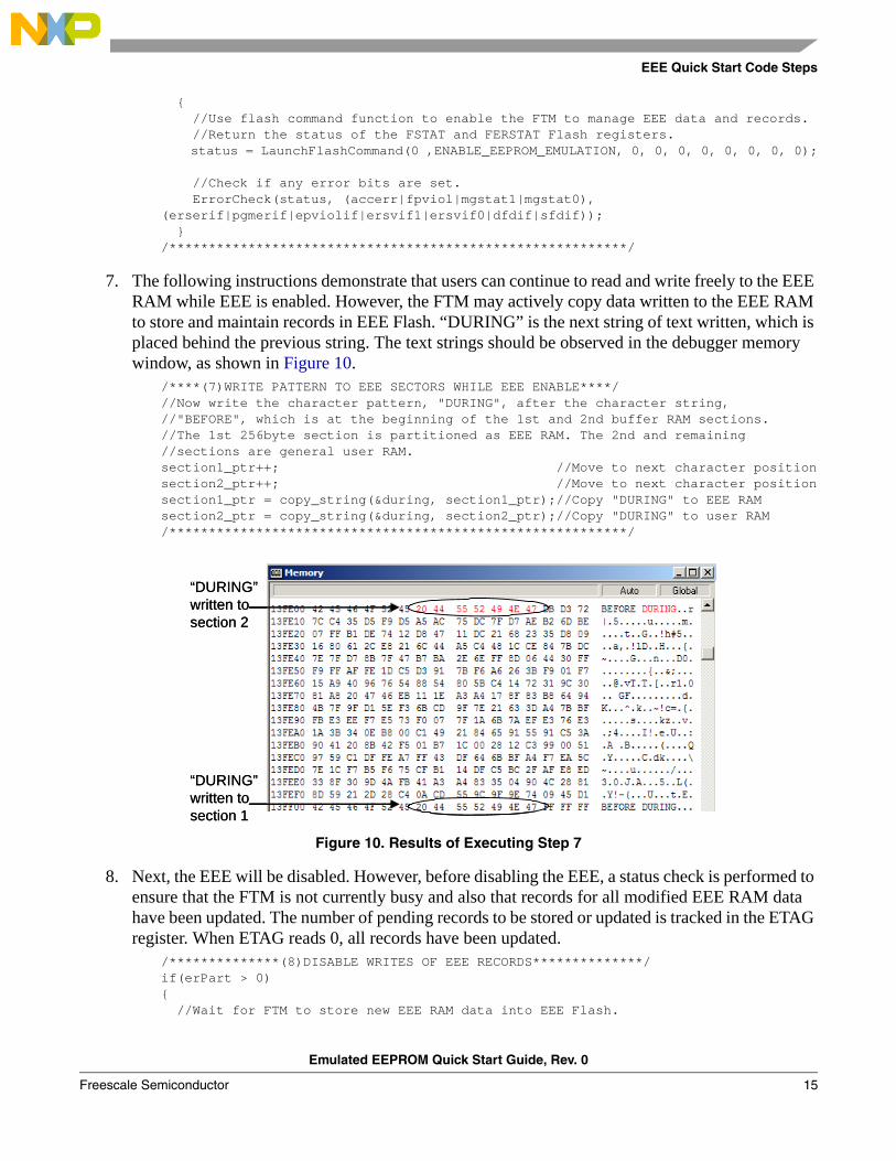
7. The following instructions demonstrate that users can continue to read and write freely to the EEE RAM while EEE is enabled. However, the FTM may actively copy data written to the EEE RAM to store and maintain records in EEE Flash. “DURING” is the next string of text written, which is placed behind the previous string. The text strings should be observed in the debugger memory window, as shown in Figure 10.
/****(7)WRITE PATTERN TO EEE SECTORS WHILE EEE ENABLE****///Now write the character pattern, "DURING", after the character string,//"BEFORE", which is at the beginning of the 1st and 2nd buffer RAM sections.//The 1st 256byte section is partitioned as EEE RAM. The 2nd and remaining//sections are general user RAM.section1_ptr++; //Move to next character positionsection2_ptr++; //Move to next character positionsection1_ptr = copy_string(&during, section1_ptr);//Copy "DURING" to EEE RAMsection2_ptr = copy_string(&during, section2_ptr);//Copy "DURING" to user RAM/**********************************************************/
Figure 10. Results of Executing Step 7
8. Next, the EEE will be disabled. However, before disabling the EEE, a status check is performed to ensure that the FTM is not currently busy and also that records for all modified EEE RAM data have been updated. The number of pending records to be stored or updated is tracked in the ETAG register. When ETAG reads 0, all records have been updated.
/**************(8)DISABLE WRITES OF EEE RECORDS**************/if(erPart > 0){
//Wait for FTM to store new EEE RAM data into EEE Flash.
“DURING”written to section 2
“DURING”written to section 1
“DURING”written to section 2
“DURING”written to section 1
Emulated EEPROM Quick Start Guide, Rev. 0
Freescale Semiconductor 15
EEE Quick Start Code Steps
while(FSTAT_MGBUSY || ETAG){//Wait for FTM to finish writing data records to EEE Flash.
}
//Use to DISable the FTM from managing EEE data and records.//Return the status of the FSTAT and FERSTAT Flash registers.status = LaunchFlashCommand(0 ,DISABLE_EEPROM_EMULATION, 0, 0, 0, 0, 0, 0, 0, 0);
//Check if any error bits are set.ErrorCheck(status, (accerr|fpviol|mgstat1|mgstat0), (erserif|pgmerif|epviolif|ersvif1|ersvif0|dfdif|sfdif));
}#endif/************************************************************/
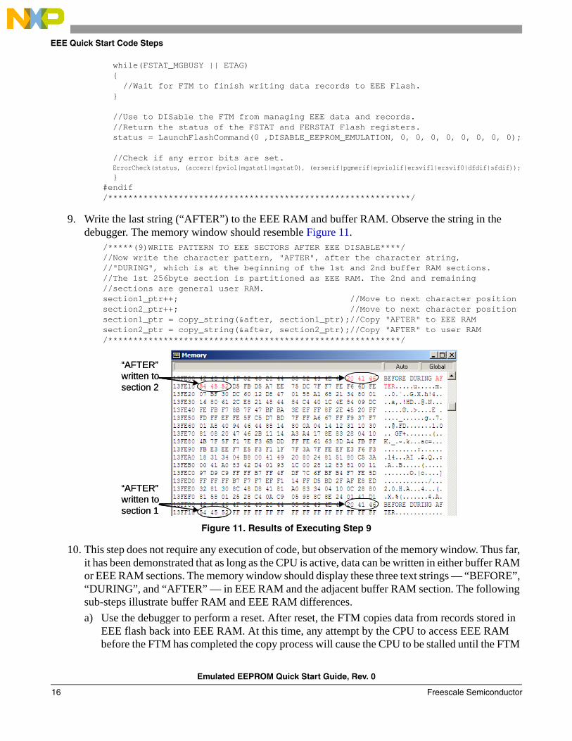
9. Write the last string (“AFTER”) to the EEE RAM and buffer RAM. Observe the string in the debugger. The memory window should resemble Figure 11.
/*****(9)WRITE PATTERN TO EEE SECTORS AFTER EEE DISABLE****///Now write the character pattern, "AFTER", after the character string,//"DURING", which is at the beginning of the 1st and 2nd buffer RAM sections.//The 1st 256byte section is partitioned as EEE RAM. The 2nd and remaining//sections are general user RAM.section1_ptr++; //Move to next character positionsection2_ptr++; //Move to next character positionsection1_ptr = copy_string(&after, section1_ptr);//Copy "AFTER" to EEE RAMsection2_ptr = copy_string(&after, section2_ptr);//Copy "AFTER" to user RAM/**********************************************************/
Figure 11. Results of Executing Step 9
10. This step does not require any execution of code, but observation of the memory window. Thus far, it has been demonstrated that as long as the CPU is active, data can be written in either buffer RAM or EEE RAM sections. The memory window should display these three text strings — “BEFORE”, “DURING”, and “AFTER” — in EEE RAM and the adjacent buffer RAM section. The following sub-steps illustrate buffer RAM and EEE RAM differences.a) Use the debugger to perform a reset. After reset, the FTM copies data from records stored in
EEE flash back into EEE RAM. At this time, any attempt by the CPU to access EEE RAM before the FTM has completed the copy process will cause the CPU to be stalled until the FTM
“AFTER”written to section 2
“AFTER”written to section 1
“AFTER”written to section 2
“AFTER”written to section 1
Emulated EEPROM Quick Start Guide, Rev. 0
Freescale Semiconductor16

EEE Quick Start Code Steps
has finished. The memory window should resemble Figure 12. Notice that the text string “AFTER” has disappeared from the EEE RAM. This is because no record of this string at this address was stored in EEE flash. Instead, the FTM returned all bytes of this address back to an erased state. Conversely, all three strings in the adjacent section of buffer RAM still remain despite the fact that the buffer RAM is volatile memory. This is because the MCU has not been power cycled.
Figure 12. EEE RAM and Buffer RAM after Reset
b) Now exit the debugger application. Power cycle the MCU to force all buffer RAM and EEE RAM to lose data. Reconnect to the MCU with the debugger; this can be done by reprogramming the same code back into the MCU.
c) Without executing any code, observe the memory window and notice that all three strings have disappeared from the buffer RAM. The absence of these strings illustrates the volatility of the buffer RAM. The EEE RAM, however, still has the “BEFORE” and “DURING” strings since they were copied from EEE flash by the FTM. This feature allows the FTM to emulate EEPROM using flash and RAM resources.
“AFTER”has been overwritten by the FTM after reset.
“AFTER”has been overwritten by the FTM after reset.
Strings no longer present in buffer RAM
Strings remain in EEE RAM
Strings no longer present in buffer RAM
Strings remain in EEE RAM
Emulated EEPROM Quick Start Guide, Rev. 0
Freescale Semiconductor 17
Summary
7 SummaryThe EEEPROM feature of the S12X flash module is the newest enhancement allowing users the flexibility to configure the behavior of memory in the EEPROM region. After completing this example, users should understand the following points:
• The location of the EEPROM region and its physical subcomponents: buffer RAM and data flash• The possible configurations of the EEPROM region• The FTM command execution flow• The necessity of always performing error checks after each FTM command execution• How data behaves when written in buffer RAM and EEE RAM
— before EEE is enabled— while EEE is enabled— after EEE is disabled
• That when EEE is partitioned, the CPU is stalled after a reset until the FTM has finished copying data from records in EEE flash back into EEE RAM
Although this application note highlights some of the characteristics of EEE, more details are available. See Freescale application note AN3490, “Overview of the MC9S12XE Emulated EEPROM,” for a broader overview of EEE.
Emulated EEPROM Quick Start Guide, Rev. 0
Freescale Semiconductor18

THIS PAGE IS INTENTIONALLY BLANK
Emulated EEPROM Quick Start Guide, Rev. 0
Freescale Semiconductor 19

Document Number: AN3743Rev. 010/2008
How to Reach Us:
Home Page:www.freescale.com
Web Support:http://www.freescale.com/support
USA/Europe or Locations Not Listed:Freescale Semiconductor, Inc.Technical Information Center, EL5162100 East Elliot RoadTempe, Arizona 85284+1-800-521-6274 or +1-480-768-2130www.freescale.com/support
Europe, Middle East, and Africa:Freescale Halbleiter Deutschland GmbHTechnical Information CenterSchatzbogen 781829 Muenchen, Germany+44 1296 380 456 (English)+46 8 52200080 (English)+49 89 92103 559 (German)+33 1 69 35 48 48 (French)www.freescale.com/support
Japan:Freescale Semiconductor Japan Ltd.HeadquartersARCO Tower 15F1-8-1, Shimo-Meguro, Meguro-ku,Tokyo 153-0064Japan0120 191014 or +81 3 5437 [email protected]
Asia/Pacific:Freescale Semiconductor Hong Kong Ltd.Technical Information Center2 Dai King StreetTai Po Industrial EstateTai Po, N.T., Hong Kong+800 2666 [email protected]
For Literature Requests Only:Freescale Semiconductor Literature Distribution CenterP.O. Box 5405Denver, Colorado 802171-800-441-2447 or 303-675-2140Fax: [email protected]
Information in this document is provided solely to enable system and software implementers to use Freescale Semiconductor products. There are no express or implied copyright licenses granted hereunder to design or fabricate any integrated circuits or integrated circuits based on the information in this document.
Freescale Semiconductor reserves the right to make changes without further notice to any products herein. Freescale Semiconductor makes no warranty, representation or guarantee regarding the suitability of its products for any particular purpose, nor does Freescale Semiconductor assume any liability arising out of the application or use of any product or circuit, and specifically disclaims any and all liability, including without limitation consequential or incidental damages. “Typical” parameters that may be provided in Freescale Semiconductor data sheets and/or specifications can and do vary in different applications and actual performance may vary over time. All operating parameters, including “Typicals”, must be validated for each customer application by customer’s technical experts. Freescale Semiconductor does not convey any license under its patent rights nor the rights of others. Freescale Semiconductor products are not designed, intended, or authorized for use as components in systems intended for surgical implant into the body, or other applications intended to support or sustain life, or for any other application in which the failure of the Freescale Semiconductor product could create a situation where personal injury or death may occur. Should Buyer purchase or use Freescale Semiconductor products for any such unintended or unauthorized application, Buyer shall indemnify and hold Freescale Semiconductor and its officers, employees, subsidiaries, affiliates, and distributors harmless against all claims, costs, damages, and expenses, and reasonable attorney fees arising out of, directly or indirectly, any claim of personal injury or death associated with such unintended or unauthorized use, even if such claim alleges that Freescale Semiconductor was negligent regarding the design or manufacture of the part.
RoHS-compliant and/or Pb-free versions of Freescale products have the functionality and electrical characteristics as their non-RoHS-compliant and/or non-Pb-free counterparts. For further information, see http://www.freescale.com or contact your Freescale sales representative.
For information on Freescale’s Environmental Products program, go to http://www.freescale.com/epp.
Freescale™ and the Freescale logo are trademarks of Freescale Semiconductor, Inc. All other product or service names are the property of their respective owners.© Freescale Semiconductor, Inc. 2008. All rights reserved.