Embed Size (px)
Citation preview
First published in July 1999
National Pollutant Inventory
Emission EstimationTechnique Manual
for
The Electronics andComputer Industry
The Computer and Electronics Industry i
EMISSION ESTIMATION TECHNIQUESFOR
THE ELECTRONICS AND COMPUTER INDUSTRY
TABLE OF CONTENTS
1.0 INTRODUCTION ......................................................................................................... 12.0 PROCESS DESCRIPTION AND EMISSION SOURCES ................................................... 2
2.1 Semiconductors.................................................................................................. 22.2 Printed Circuit Boards...................................................................................... 92.3 Cathode Ray Tubes .......................................................................................... 16
3.0 EMISSION ESTIMATION TECHNIQUES: ACCEPTABLE RELIABILITY ANDUNCERTAINTY........................................................................................................... 213.1 Mass Balance...................................................................................................... 223.2 Emission Factors................................................................................................ 233.3 Direct Measurement or Sampling Data........................................................... 243.4 Engineering Calculations ................................................................................. 25
4.0 ESTIMATING EMISSIONS........................................................................................... 264.1 Using Mass Balance .......................................................................................... 28
4.1.1 Estimating Emissions to Air .......................................................................... 284.1.2 Estimating Emissions to Water ..................................................................... 304.1.3 Estimating Emissions to Land........................................................................ 31
4.2 Using Sampling Data ........................................................................................ 314.2.1 Estimating Emissions to Air .......................................................................... 314.2.2 Estimating Emissions to Water ..................................................................... 33
4.3 Using Emission Factors .................................................................................... 334.3.1 Estimating Emissions to Air........................................................................... 334.3.2 Estimating Emissions to Water ..................................................................... 35
4.4 Using Engineering Calculations ...................................................................... 364.4.1 Estimating Emissions Using Mass Transfer Kinetics .................................... 364.4.2 Estimating Emissions from Spills ................................................................. 374.4.3 Estimating Fugitive Emissions....................................................................... 40
4.5 Other Emission Sources ................................................................................... 425.0 REFERENCES ............................................................................................................ 44
The Computer and Electronics Industry ii
THE ELECTRONICS AND COMPUTER INDUSTRY
LIST OF FIGURES, TABLES AND EXAMPLES
Figure 1 - Process Flow Diagram of a Semiconductor Manufacturer.......................... 26
Table 1 - Sectors of the Electronics and Computer Industry ...................................... 22 - Substances Used in Photolithography for Semiconductors ......................... 53 - Emissions from Semiconductor Manufacturing ........................................... 94 - Chemicals Used in Lamination, Drilling, and Cleaning............................... 115 - Chemicals Used in Printed Circuit Board Photolithography ...................... 136 - Substances Used During Etching ................................................................... 137 - Materials Used in Copper and Tin-Lead Electro and Electroless PlatingProcesses................................................................................................................. 148 - Emissions from Printed Circuit Board Manufacture................................... 169 - Emissions Generated from Cathode Ray Tube Manufacture ..................... 2110 - Summary of EET Reliability for Electronic and ComputerManufacturing Processes...................................................................................... 2511 - List of Variables and Symbols ...................................................................... 2712 - Concentration of NPI-Listed Substances in Untreated Wastewaterfrom US Semiconductor Manufacturing Facilities ............................................ 3613 - Correlation Equations, Default Zero Emission Rates, and PeggedEmission Rates for Estimating Fugitive Emissions............................................ 4114 - Emission Factors for Equipment Leaks....................................................... 42
Example 1 - Using a Mass Balance to Estimate VOC Emissions.................................... 28 2 - Using a Mass Balance to Speciate VOC Emissions..................................... 30 3 - Estimating Ammonia Emissions to Atmosphere......................................... 33 4 - Using Emission Factors to Estimate Emissions to Air................................ 34 5 - Using Emission Factors to Estimate Emissions to Water .......................... 35 6 - Using Mass Transfer Kinetics....................................................................... 37 7 - Calculating Emissions from Chemical Spills .............................................. 39 8 - Estimating Fugitive Emissions...................................................................... 42
The Computer and Electronics Industry 1
1.0 Introduction
The purpose of all Emission Estimation Technique (EET) manuals in this series is to assistAustralian manufacturing, industrial, and service facilities to report emissions of listed substancesto the National Pollutant Inventory (NPI). This manual describes the procedures and recommendedapproaches for estimating emissions from facilities engaged in electronics and computermanufacturing.
EET MANUAL : The Electronics & Computer Industry
HANDBOOK : Computers and Electronic Equipment Manufacturing
ANZSIC CODE : 2841, 2849
This manual was drafted by the NPI Unit of the Queensland Department of Environment andHeritage on behalf of the Commonwealth Government. It has been developed through a process ofnational consultation involving State and Territory environmental authorities and key industrystakeholders.
The Computer and Electronics Industry 2
2.0 Process Description and Emission Sources
The electronics and computer industry is comprised of five major groups: telecommunications,computers, industrial electronics, consumer electronics, and semiconductors. Many segments of theelectronics and computer industry are interdependent and share common manufacturing processes.Products produced by the electronics and computer industry are shown in Table 1.
Table 1 - Sectors of the Electronics and Computer IndustryIndustry Industry
Transformers Motors and Generators
Communication Equipment Printed Circuit Boards & Semiconductors
Integrated Circuits Cathode Ray Tubes
Source: Queensland Department of Environment and Heritage, 1998.
Due to the vast variety of equipment manufactured by the electronics and computer industries, thisSection focuses on the distinct equipment and products that raise environmental issues and whichare most likely to be included by manufacturing facilities reporting to the NPI. This equipmentincludes:
• Semiconductors and Related Devices;• Printed Circuit Boards (also called printed wiring boards); and• Cathode Ray Tubes.
The Section focuses on semiconductors and not integrated circuits because integrated circuits areused to produce semiconductors and most electronic devices manufactured today are multipledevices/circuit chips. Semiconductors, although accounting for only a tiny portion of industry sales,are crucial to electronic products and pose numerous environmental concerns. Printed circuit boardsand cathode ray tubes also raise environmental concerns from their manufacturing processes andfacilities producing any of these products are likely to trigger NPI reporting obligations.
2.1 Semiconductors
Semiconductors can serve one of two purposes:
(1) they act as a conductor by guiding or moving an electrical current; or(2) as an insulator by preventing the passage of heat or electricity.
Semiconductors are used in computers, consumer electronic products, telecommunicationequipment, industrial machinery, transportation equipment, and military hardware. Typicalfunctions of semiconductors in these products include information processing, display purposes,power handling, data storage, signal conditioning, and conversion between light and electricalenergy sources. Computers, however, remain the principal end-use of semiconductors, constitutingaround 40 percent of the market.
Semiconductors are made of solid crystalline material, usually silicon, formed into a simple diodeor many integrated circuits. A simple diode is an individual circuit that performs a single function
The Computer and Electronics Industry 3
affecting the flow of electrical current. Integrated circuits combine two or more diodes. Up toseveral thousand integrated circuits can be formed on the wafer, although 200 to 300 integratedcircuits are usually formed. The area on the wafer occupied by integrated circuits is called a chip ordie.
The semiconductor manufacturing process is complex and may require that several of the steps berepeated to complete the process. To simplify this description, the process has been broken downinto five steps:
• design;• crystal processing;• wafer fabrication;• final layering and cleaning; and• assembly.
The primary reason that semiconductors fail is contamination, particularly the presence of anymicroscopic residue (including chemicals and particulates) on the surface of the base material, orcircuit path. Therefore, a clean environment is essential to the manufacture of semiconductors.Cleaning operations occur before and after many of the manufacturing process steps. Wetprocessing, during which semiconductor devices are repeatedly dipped, immersed, or sprayed withsolutions, is commonly used to minimise the risk of contamination.
Step One: Design
As with any manufacturing process, the need for a particular type of product must be identified andprocess specifications must be developed to address that need. In the case of semiconductors, thecircuit is designed using computer modelling techniques. Computer simulation is used to developand test layouts of the circuit path. Then, patterning masks, which are like stencils, are fabricated,manufacturing equipment is selected, and operating conditions are set. All of these steps occur priorto actually producing a semiconductor.
Step Two: Crystal Processing
Wafers, which consist of thin sheets of crystalline material, are the starting phase of semiconductorproduction. Silicon, in the form of ingots, is the primary crystalline material used in the productionof 99 percent of semiconductors. Silicon crystals are actually grown using controlled techniques toensure a uniform crystalline structure. Because crystals of pure silicon are poor electricalconductors, controlled amounts of chemical impurities or dopants are added during thedevelopment of silicon ingots to enhance their semiconducting properties. Dopants are typicallyapplied using diffusion or ion implantation processes. Dopants eventually form the circuits thatcarry the flow of current.
• Diffusion is a chemical process, which exposes the regions of the silicon surface to vapours ofthe metal additive (dopant) while maintaining high temperatures. The process ends when theadditives migrate to the proper depth and reach the appropriate concentration in the silicon wafer.
• Ion Implantation is a process that allows for greater control of the location and concentrationof dopants added to the wafer. Metal dopants are ionised and accelerated to a high speed.
The Computer and Electronics Industry 4
Either doping process can be used in semiconductor manufacturing. The NPI-listed substances:antimony, arsenic, phosphorus, and boron compounds are the dopant materials most commonlyused for silicon-based semiconductors. Other dopants include aluminium, gallium, gold,germanium, silicon, tin, tellurium, and the NPI-listed metals beryllium and magnesium. Emissionsand solid wastes containing the listed substances: antimony, arsenic, phosphorus, and boron may begenerated in the wastewater as a result of ion implantation or diffusion. Excess dopant gases,contaminated carrier gases, and out-gassed dopant gases from semiconductor materials may also begenerated.
Most semiconductor manufacturers obtain single crystal silicon ingots from other manufacturingfirms. Ingots are sliced into round wafers approximately 0.76mm thick and then rinsed. The wafersare further prepared by mechanical or chemical means. A wafer’s surface may be mechanicallyground, smoothed, and polished, as well as chemically etched so that the surface is smooth and freeof oxides and contaminants. Chemical etching removes organic contaminants using cleaningsolvents and removes damaged surfaces using acid solutions. Chemical etching is usually followedby a deionised water rinse and drying with compressed air or nitrogen. In some cases, bare siliconwafers are cleaned using ultrasound techniques, which involve potassium chromate or other mildlyalkaline solutions.
Etching is a method of cutting into, or imprinting on, the surface of a material. Several etchingprocesses can be used on semiconductors, as well as integrated circuits and printed circuit boards.Wet etching uses acid solutions to cut patterns into the metal. Dry etching involves reactive gasesand is rapidly becoming the method of choice for high resolution. Dry etching processes use varioushalogenated or non-halogenated gaseous compounds.
In the semiconductor industry, dry plasma etching, reactive ion etching, and ion milling processesare being developed to overcome the limitations of wet chemical etching. Dry plasma etching, themost advanced technique, allows for etching of fine lines and features without the loss of definition.This process forms a plasma layer above the surface to be etched by combining large amounts ofenergy with low-pressure gases. The gases usually contain halogens.
Materials used during the wet etching process may include the following NPI-listed substances:sulfuric, phosphoric, nitric, hydrofluoric, and hydrochloric acids; ethylene glycol; and solutions ofammonium. Other etching materials used include hydrogen peroxide and other hydroxide solutionsand ferric or potassium compounds. Materials used during the dry etching process may includechlorine, hydrogen bromide, carbon tetrafluoride, sulfur hexafluoride, trifluoromethane, fluorine,fluorocarbons, boron trichloride, hydrogen, oxygen, helium, and argon. Typical solvents andcleaning agents include the NPI-listed substances acetone, xylenes, glycol ethers, together withdeionised water and isopropyl alcohol. The most commonly used cleaning solution insemiconductor manufacturing includes a variety of proprietary products containing a combinationof hydrogen peroxide and sulfuric acid.
Emissions generated include acid fumes and organic solvent vapours from cleaning, etching, resistdrying, developing, and resist stripping operations. Hydrogen chloride vapours may also be emittedduring the etching process.
Step Three: Wafer Fabrication
Wafers are usually fabricated in batches of 25 to 40. Wafer preparation begins with an oxidationstep.
• Oxidation is a process in which a film of silicon dioxide is formed on the exterior surface of thesilicon wafer. Thermal oxidation takes place in a tube furnace with controlled, high temperatures
The Computer and Electronics Industry 5
and a controlled atmosphere. Oxidation is a reaction between the silicon wafer surface and anoxidant gas, such as oxygen or steam. This process may be needed as a preliminary step beforediffusion or ion implantation (doping). This layer protects the wafer during further processing.Following oxidation, the wafer surface is thoroughly cleaned and dried.
Materials used during oxidation include silicon dioxide, acids (hydrofluoric), and solvents.Materials such as oxygen, hydrogen chloride, nitrogen, trichloroethane, and trichloroethylene(perchloroethylene) may also be used.
Emissions generated from this process include spent solvents (non-halogenated) including xylenes,acetone, ethyl acetate, styrene, methyl isobutyl ketone, and methanol as well as spent acids andsolvents in the wastewater.
Next, patterns are imprinted onto the substrate using photolithography (also referred to aslithography) and etching processes. Photolithography is the most crucial step in semiconductormanufacturing because it sets a device’s dimensions - incorrect patterns affect the electricalfunctions of the semiconductor.
• Photolithography is a process similar to photoprocessing techniques and other etchingprocesses. The silicon wafer is coated uniformly with a thin film of resist. A glass plate or mask iscreated with the circuit pattern, and the pattern is imprinted in one of several ways. One type ofoptical photolithography is the projection of x-rays through a special mask close to the silicon slice.Another type of optical photolithography, one that does not need a mask, is electron-beam directpatterning, which uses a controllable electron beam and an electron sensitive resist. Once the patternis developed, some areas of the wafer are clear and the rest are covered with resist.
Two types of photoresists can be used during semiconductor production:
• Positive photoresists are chemicals that are made more soluble, after exposure to radiation.During development, the developer removes the resist that was exposed to radiation.
• Negative photoresists are chemicals that polymerise and stabilise upon exposure to radiation.During development, the developer removes the resist that was protected from radiation.
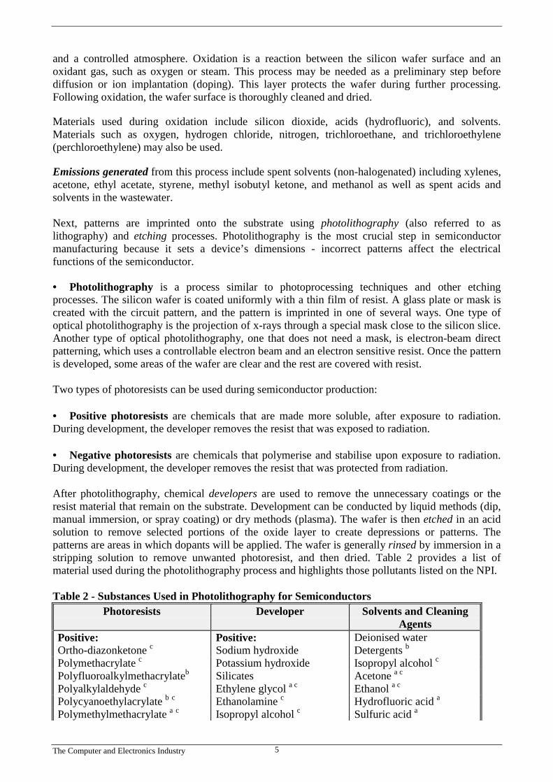
After photolithography, chemical developers are used to remove the unnecessary coatings or theresist material that remain on the substrate. Development can be conducted by liquid methods (dip,manual immersion, or spray coating) or dry methods (plasma). The wafer is then etched in an acidsolution to remove selected portions of the oxide layer to create depressions or patterns. Thepatterns are areas in which dopants will be applied. The wafer is generally rinsed by immersion in astripping solution to remove unwanted photoresist, and then dried. Table 2 provides a list ofmaterial used during the photolithography process and highlights those pollutants listed on the NPI.
Table 2 - Substances Used in Photolithography for SemiconductorsPhotoresists Developer Solvents and Cleaning
AgentsPositive: Positive: Deionised waterOrtho-diazonketone c Sodium hydroxide Detergents bPolymethacrylate c Potassium hydroxide Isopropyl alcohol cPolyfluoroalkylmethacrylateb Silicates Acetone a c
Polyalkylaldehyde c Ethylene glycol a c Ethanol a c
Polycyanoethylacrylate b c Ethanolamine c Hydrofluoric acid aPolymethylmethacrylate a c Isopropyl alcohol c Sulfuric acid a
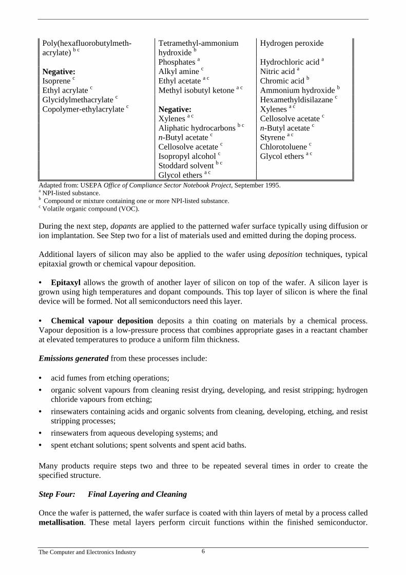
The Computer and Electronics Industry 6
Poly(hexafluorobutylmeth-acrylate) b c
Tetramethyl-ammoniumhydroxide b
Hydrogen peroxide
Phosphates a Hydrochloric acid aNegative: Alkyl amine c Nitric acid aIsoprene c Ethyl acetate a c Chromic acid bEthyl acrylate c Methyl isobutyl ketone a c Ammonium hydroxide bGlycidylmethacrylate c Hexamethyldisilazane cCopolymer-ethylacrylate c Negative: Xylenes a c
Xylenes a c Cellosolve acetate cAliphatic hydrocarbons b c n-Butyl acetate cn-Butyl acetate c Styrene a c
Cellosolve acetate c Chlorotoluene cIsopropyl alcohol c Glycol ethers a c
Stoddard solvent b c
Glycol ethers a c
Adapted from: USEPA Office of Compliance Sector Notebook Project, September 1995.a NPI-listed substance.b Compound or mixture containing one or more NPI-listed substance.c Volatile organic compound (VOC).
During the next step, dopants are applied to the patterned wafer surface typically using diffusion orion implantation. See Step two for a list of materials used and emitted during the doping process.
Additional layers of silicon may also be applied to the wafer using deposition techniques, typicalepitaxial growth or chemical vapour deposition.
• Epitaxyl allows the growth of another layer of silicon on top of the wafer. A silicon layer isgrown using high temperatures and dopant compounds. This top layer of silicon is where the finaldevice will be formed. Not all semiconductors need this layer.
• Chemical vapour deposition deposits a thin coating on materials by a chemical process.Vapour deposition is a low-pressure process that combines appropriate gases in a reactant chamberat elevated temperatures to produce a uniform film thickness.
Emissions generated from these processes include:
• acid fumes from etching operations;• organic solvent vapours from cleaning resist drying, developing, and resist stripping; hydrogen
chloride vapours from etching;• rinsewaters containing acids and organic solvents from cleaning, developing, etching, and resist
stripping processes;• rinsewaters from aqueous developing systems; and• spent etchant solutions; spent solvents and spent acid baths.
Many products require steps two and three to be repeated several times in order to create thespecified structure.
Step Four: Final Layering and Cleaning
Once the wafer is patterned, the wafer surface is coated with thin layers of metal by a process calledmetallisation. These metal layers perform circuit functions within the finished semiconductor.
The Computer and Electronics Industry 7
External connections to the silicon wafer are provided by evaporation of thin metal films onto areasof the semiconductor chip surface in a vacuum. Almost every metal can be used to make thiselectrical connection to the silicon; aluminium, platinum, titanium, nickel, chromium, silver,copper, tungsten, gold, germanium, and tantalum are the most common. Argon gas is also used insome operations. Sputtering and high vacuum evaporation are two types of metallisation.
• Sputtering (also called partial vacuum evaporation) is a physical, rather than chemical process.This process occurs in a vacuum chamber which contains a target (solid slab of the film material)and the wafers. Argon gas is introduced in the chamber and ionised to a positive charge. Thepositively charged argon atoms accelerate toward and strike the target, dislodging the target atoms.The dislodged atoms are deposited onto the wafer surface. A uniform thickness of the coating isproduced over the silicon slice.
• High vacuum evaporation is a process that uses an electron beam, a ceramic bar heated bythermal resistance, or a wire heated by electrical resistance. This method coats the surface of thewafer with metal.
Photolithography and etching are also used to remove any unnecessary metal using chlorinatedsolvents or acid solutions. Emissions generated include: acid fumes and organic solvent vapoursfrom cleaning, etching, resist drying, developing, and resist stripping; liquid organic wastes;aqueous metals; and wastewater contaminated with spent cleaning solutions.
In the next step, passivation is used to apply a final layer of oxide over the wafer surface to providea protective seal over the circuit. This coating protects the semiconductor from exterior influencesand may range in thickness from a single layer of silicon dioxide to a relatively thick deposit ofspecial glass. It also insulates the chip from unwanted contact with other external metal contacts.Materials used to form the passivation layer are silicon dioxide or silicon nitride.
After all layers have been applied to the wafer, the wafer is typically rinsed in deionised water. Theback of the wafer is then mechanically ground (also called lapping or backgrinding) to removeunnecessary material. A film of gold may be applied to the back of the wafer by an evaporationprocess to aid the connection of leads to the bonding pads during a later process step.
Testing with alcohol compounds is conducted to ensure that each chip is performing the operationsfor which it was designed. Chips that do not meet specifications are marked with an ink droplet fordiscard during assembly operations. The wafer is cleaned again after testing, using solvents such asdeionised water, isopropyl alcohol, acetone, and methanol.
Emissions generated from these processes include:
• spent solvents and acids in the wastewater and rinsewater from cleaning, developing, etching,resist stripping, and rinsing processes;
• acid fumes and organic solvent vapours from cleaning, rinsing, resist drying, developing, andresist stripping;
• spent silicon dioxide or nitride;• hydrogen chloride vapours from etching;• rinsewaters from aqueous developing systems;• spent etchant solutions;• spent acid baths; and• spent solvents.
Step Five: Assembly
The Computer and Electronics Industry 8
Semiconductors are assembled by mounting chips onto a metal frame, connecting the chips to metalstrips (leads), and enclosing the device to protect against mechanical shock and the externalenvironment. There are many types of packaging such as plastic or ceramic.
Each package contains five parts:
1. the dye (ie. the chip);2. the lead frame of the package;3. the dye-attach pad;4. the wire bond; and5. the moulded encapsulant (ie. the plastic housing).
This section describes how plastic packages are assembled. All semiconductor packages whetherplastic or ceramic share the same basic parts and are assembled using the same general processes.
The lead frame and leads provide the connections for the electronic components.
• The punching process consists of an array of small mechanical punches that remove sections ofthe metal sheet until the lead frame is complete. The leads are cleaned with water-based cleaningsystems. Historically, manufacturers used chlorinated fluoro-carbons (CFCs) or other solvents toremove cutting fluids. The use of CFCs in Australia has been phased out during the last decade, dueto their role in the depletion of the stratospheric ozone, and the manufacture and import of thesechemicals has not been undertaken since early in 1996. Since this time, the use of CFCs in thesemiconductor industry has been replaced by other solvents. The lead frame is coated with a layerof photoresist, exposed, and developed. The manufacturer etches the lead frame, removes thephotoresist, and cleans the lead frame again with water-based cleaning systems.
• If the lead frames are etched, the process is similar to that used during the manufacturing ofprinted circuit boards. Acids or metal chlorides are usually used during etching. Sometimesammonia is used to stabilise the metal chloride. The photoresist contain solvents (such astrichloroethylene or TCE) that are baked out and generate VOC emissions. Developers that aretypically used include either an amine or metal hydroxide. Once the photoresist is removed, it iscleaned with solvents such as a mild hydrochloric acid (HCl) solution with a brightener thatcontains sulfuric acid (H2SO4).
Emissions generated during punching or etching may include:
• spent organic vapours generated from cleaning, resist drying, developing, and resist stripping;• spent cleaning solutions;• rinsewaters contaminated with organic solvents; and• spent aqueous developing solutions.
Scrap copper or copper alloy may be recycled during the punching process.
The chip is then attached to an attach pad, with a substance such as an epoxy material (thermosetplastic). Once mounted, the chips are inspected. The chip parts are bonded to the leads of thepackage with tiny gold or aluminium wires. A package may have between two and 48 wire bonds.The assembly is cleaned and inspected again. The combined components are then placed into amoulding press, which encases the chip, wire bonds, and portions of the leads in plastic. After themoulding compound cures and cools around the package, the package is heated again to ensure that
The Computer and Electronics Industry 9
the plastic is completely cured. Excess material is removed using a chemical or mechanical deflashprocess. M-Pyrol is one organic solvent used during the deflash process. The final steps in packagefabrication include trimming and forming the leads.
Emissions generated during these steps include excess epoxy/thermoset plastic; antimony trioxide(from the moulding process); and spent organic solvents.
Table 3 summarises the emissions from all semiconductor manufacturing processes.
Table 3 - Emissions from Semiconductor ManufacturingProcess Air
EmissionsWater
EmissionsSolid-WasteEmissions
CrystalPreparation
Acid fumes,VOCs,dopantgases
Spent deionised water, spentsolvents, spent alkalinecleaning solutions, spentacids, spent resist material
WaferFabrication
VOCs anddopantgases
Spent solvents, spent acids,aqueous metals, spent etchantsolution, and spent aqueousdeveloping solutions
Spent non-halogenatedsolvents: xylene, acetone,ethyl acetate, ethyl ether,ethyl benzene, methylisobutyl ketone, methanol,cyclohexanone, and n-butylalcohol in still bottoms
FinalLayering andCleaning
Acid fumesand VOCs
Spent deionised water, spentsolvents, spent acids, spentetchants, spent aqueousdeveloping solutions, spentcleaning solutions, aqueousmetals, and chromium
Spent solvents
Assembly VOCs Spent cleaning solutions,spent solvents, and aqueousdeveloping solutions
Spent epoxy material andspent solvents
Adapted from: USEPA Office of Compliance Sector Notebook Project, September 1995.
2.2 Printed Circuit Boards
Computers are also the largest Australian market for printed circuit boards (PCBs), withcommunications being the second largest application market. PCBs and assemblies are used inmany electronic products such as electronic toys, radios, television sets, electrical wiring in cars,avionics, computers, biotechnology, medical devices, digital imaging technology, and industrialcontrol equipment.
PCBs are the physical structures on which electronic components such as semiconductors andcapacitors are mounted. The combination of PCBs and electronic components is an electronicassembly or printed circuit assembly (PCA). The manufacture of PCBs is the most chemical-intensive process in the building of a computer workstation.
The Computer and Electronics Industry 10
PCBs are subdivided into single-sided, double-sided, multilayer, and flexible boards. Multilayerboards are manufactured in the same way as single and double-sided boards, except that conductingcircuits are etched on both the external and internal layers. Multilayer boards allow for increasedcomplexity and density. PCBs are produced using three methods: additive, subtractive, or semi-additive technology. The subtractive process accounts for a significant majority, perhaps 80 percentor more, of PCB manufacturing.
The conventional subtractive manufacturing process begins with a board, consisting of epoxy resinand fibreglass, onto which patterns are imaged. In most operations, conducting material, usuallycopper, is bonded onto the substrate surface to form copper-clad laminate. After drilling holesthrough the laminate and making those holes conductive, unwanted copper is etched off, leavingcopper patterns. The patterns on the board form the electric circuits that conduct electricity.Multilayer boards typically use metals such as platinum, palladium, and copper to form electriccircuits. Specialised PCBs may use nickel, silver, or gold.
Additive technology is used less often than subtractive technology because it is a more difficult andcostly production process. This capital-intensive technology is used primarily for smallinterconnection components used in multi-chip devices. The production process begins with a baseplate upon which a dielectric material is deposited. An interconnecting layer of copper is platedonto the dielectric layer, which connects the layers of dielectric material and copper. Copper postsare plated-up and another layer of dielectric material is deposited exposing the posts. The nextinterconnecting layer is plated and makes contact with the posts. Layers of dielectric material,copper, and copper posts are added to complete the chip. A lithographic process, similar to the oneused in semiconductor manufacturing, diminishes the spaces and widths of the PCB.
This section provides a simplified discussion of the steps commonly performed during conventionalsubtractive manufacturing. The actual steps and materials used by a PCB manufacturer varydepending on customer requirements and the products being manufactured. This feature of the PCBindustry ensures it is both complex and difficult to characterise the industry for NPI reportingobligations and to provide guidance in estimating emissions from PCB manufacture. Nevertheless,the following discussion attempts to provide the reader with information on the likely emissions ofNPI substances expected to arise from PCB manufacture. PCB manufacturing can be grouped intofive distinct steps:
• Board preparation;• Application of conductive coatings (plating);• Soldering;• Fabrication; and• Assembly.
Step One: Board Preparation
Board preparation begins with a lamination process. Two-side etched copper dielectric boards(consisting usually of fibreglass and epoxy resin) are separated by an insulating layer and laminatedor bonded together, usually by heat and pressure. Photographic tools are used to transfer the circuitpattern to the PCB, and computer control programs are used to control the drilling, routing, andtesting equipment. Preparing the copper-clad board involves drilling holes to establish an electricalpath between the layers and to mount components. The boards are then mechanically cleaned toremove drilling wastes (that is, fine particulate contaminants, such as copper).
The Computer and Electronics Industry 11
Vapour degreasing, abrasive cleaning, chemical cleaning with alkaline solutions, acid dips, andwater rinses are techniques used to clean the boards and prepare them for the next process, namelyelectroless plating. Table 4 shows a list of materials used during the lamination, drilling, andcleaning processes.
Table 4 - Chemicals Used in Lamination, Drilling, and CleaningLamination Drilling Cleaning
Epoxies b Sulfuric acid aPotassium permanganate bAmmonium bifluoride aOxygenFluorocarbon gas b c
Acetone a c
1,1,1-Trichloroethane a c
Silica (and other abrasives)Sulfuric acid aAmmonium hydroxide aHydrochloric acid a
Source: Queensland Department of Environment and Heritage, 1998.a NPI-listed substance.b Compound or mixture containing one or more NPI-listed substance.c Volatile organic compound (VOC).
Emissions generated include:
• airborne particulates including PM10 (particulate matter with an aerodynamic diameter of lessthan or equal to 10µm), acid fumes, and organic vapours from cleaning, surface preparation, anddrilling;
• spent acid and alkaline solutions;• spent developing solutions, spent etchants and waste rinsewaters in the wastewater; and• scrap board materials and sludges from wastewater treatment.
Drilling and routing dusts (including copper) are collected and recycled.
Step Two: Electroless Plating
The first process in this step is to prepare the surfaces of the drilled holes. The holes are prepared byan etchback process to remove smeared epoxy resin and other contaminants using one of thefollowing: sulfuric or hydrochloric acid; potassium permanganate; or carbon tetrachloride, oxygen,and nitrogen. The holes are then coated with a material such as copper or graphite carbon by achemical process called electroless plating.
Electroless plating coats a uniform conducting layer of copper or other material on the entiresurface including the barrels of the holes of the prepared board without outside power sources.According to Printed Circuit Board Basics, this coating of copper is not thick enough to carry anelectrical current, but provides a base upon which additional copper can be depositedelectrolytically. Copper is the industry standard, but many are switching to direct metallisationprocesses. Chemical deposition is the technique used to coat the board. After the electroless plating,the boards are dried to prevent the board from oxidation, or rusting. The board may also be cleanedto prepare for a following electroplating process. See Table 6 for a list of materials used.
Emissions generated include:
• spent electroless copper baths;• spent catalyst solutions;• spent acid solutions;

The Computer and Electronics Industry 12
• spent electroless copper baths;• spent catalyst solutions;• spent acid solutions;• waste rinsewaters; and• sludges from wastewater treatment.
Step Three: Imaging
During imaging, circuit patterns are transferred onto the boards through photolithography or astencil printing process. Photoresist (ie. a light sensitive chemical) is applied to the board in areaswhere the circuit pattern will not be set. The board is exposed to a radiation source and developed toremove the unwanted areas of the resist layer. Stencil printing uses a printing process, such as silkscreening, to apply a protective film that forms the circuit pattern.
After photolithography, the boards are subjected to a light etching process, typically usingammoniacal etchants, to remove rust inhibitor (applied by the company that produced the materialfrom which the board is made) or other metals (usually copper). After the stencil printing process,the protective film is dried, and the exposed copper is etched away. Sulfuric acid and hydrogenperoxide are common etchants used during imaging. After plating or etching, the photoresist isremoved with a photoresist stripper.
Table 5 and Table 6 detail the materials used during photolithography and etching processes.
The Computer and Electronics Industry 13
Table 5 - Chemicals Used in Printed Circuit Board PhotolithographyResists Photopolymer Developers Photopolymer
StrippersMylar (DuPont) orMelinex (Orica) polyesterfilmVinylPhotoresists
Isopropyl alcohol cPotassium bicarbonateSodium bicarbonate1,1,1-Trichloroethane cAmines b c
Glycol ethers c
Sodium hydroxidePotassium hydroxideDichloromethane c(methylene chloride)
Source: Queensland Department of Environment and Heritage, 1998.a NPI-listed substance.b Compound or mixture containing one or more NPI-listed substance.c Volatile organic compound (VOC).
Emissions generated during the cleaning and etching processes include a wide range of solvents,many of which are NPI-listed. The solvents emitted depend on the concentration of the spentsolvents and the mixture of spent halogenated and non-halogenated solvents; spent resist material;and wastewater containing metals (copper). Other emissions generated include organic vapours andacid fumes, spent developing solutions, spent resist material, spent etchant, spent acid solutions, andsludges from wastewater treatment.
Table 6 - Substances Used During EtchingAmmonia aAmmonium chloride aAmmonium hydroxide aAmmonium persulfate aAmmonium sulfate aBoric acid aCarbon tetrachloride cChlorine aCupric chloride aHydrochloric acid a
Hydrofluoric acid aHydrogen peroxideLead aNickel aNickel chloride aNickel sulfamate aNitrate aNitric acid aNitrogenOrthophosphate a
OxygenPeptonePermanganates bSodium citrateSodium hydroxideStannous chlorideSulfuric acid aTin
Source: Queensland Department of Environment and Heritage, 1998.a NPI-listed substance.b Compound or mixture containing one or more NPI-listed substance.
Step Four: Electroplating
Electroplating is a process in which a metal is deposited on a substrate through electrochemicalreactions. Electroplating is required to build up the thickness and strength of the conducting layersto provide reliable electrical conductivity between inner layers or from one side of the PCB to theother. Electroplating can also protect against corrosion, wear, and erosion. This process involvesimmersing the article to be coated or plated into a bath containing acids, bases, or salts. Theindustry standard for this process is copper, although many are switching to direct metallisationtechniques.
The electroplating process for PCBs usually begins with the copper laminate which is coated with aplating resist (photolithography) by stencilling, leaving the area exposed to form the circuit pattern.The resist prevents the conductive material from adhering to other areas of the board and forms thecircuit pattern.
The Computer and Electronics Industry 14
The PCB plating process generally uses copper and tin-lead as plating materials, although silver,nickel, or gold, can also be used. Copper in a plating bath solution is deposited to a sufficientthickness, and a solvent or aqueous solution is applied to remove the plating resist. The coppercoating forms inter-connections between the layers and provides electrical contact for electronicparts mounted or assembled on the PCB surface. PCB manufacturers then typically electroplate atin or tin-lead solder on the board to protect the circuit pattern during the following etching orstripping processes. An acid etch solution (ammoniacal, peroxide solutions, sodium persulfate,cupric chloride, or ferric chloride) removes the exposed copper foil, leaving the thicker copperplating to form the circuit pattern. Ammoniacal and cupric chloride are the primary etchants usedby PCB manufacturers. Fluoroboric acid is used in the tin-lead plating process to keep the metalsdissolved in the solution and to ensure a consistent deposition of the tin-lead alloy onto the circuitboard.
After the plating bath, the board is rinsed with water, scrubbed, and then dried to remove thecopper, spray etch solutions, and other materials. Rinsing ends the chemical reactions during platingand prevents contamination or dragout from being released in the next bath or rinse water (dragoutis the plating solution that sticks to parts after the board has been taken out of the plating bath).Dragout can occur in any bath step, not just in one plating bath. The tin-lead layer is generallyremoved and the panel is electrically tested for irregularities in the electrical pathway and shorts.Table 7 lists materials used during electroplating processes and highlights those listed on the NPI.
Table 7 - Materials Used in Copper and Tin-Lead Electro and Electroless Plating Processes
Type of Plating Electroplating Chemicals Electroless ChemicalsCopper Copper pyrophosphate b
Orthophosphate bNitrates aAmmonia aAcid copper aCopper sulfate aSulfuric acid a
Hydrochloric acid aPalladium chlorideStannous chlorideMetallic tin pelletsSodium hydroxideCopper sulfate aFormaldehyde a
Tin-Lead Tin-Lead aFluoroboric acid bBoric acid aPeptone
Tin chlorideSodium hypophosphate bSodium citrate
Source: Queensland Department of Environment and Heritage, 1998.a NPI-listed substance.b Compound or mixture containing one or more NPI-listed substance.
The Computer and Electronics Industry 15
Emissions generated, including wastes containing NPI-listed substances, generated during platinginclude:
• photoresist skins;• sludges from wastewater treatment (containing metals and acids, lead compounds, spent cyanide
plating bath solutions, and plating bath residues from the bottom of plating baths from platingand etching operations where cyanides are used in the process);
• spent acid solutions, waste rinsewaters, spent developing solutions, spent etchant, and spentplating baths in the wastewater;
• organic vapours from spent developing solution and spent resist removal solution; and• acid and ammonia fumes.
Step Five: Soldering Coating
Solder coating is used to add solder to PCB copper component before component assembly.Manufacturers use several methods of solder coating, but all of them involve dipping the panel intomolten solder. The solder, an alloy consisting of 60 percent tin and 40 percent lead, coats the padsand holes not covered by solder mask. The excess solder is removed with a blast of hot oil or hotair. However, the hot oil or hot air does not remove the solder that has formed a chemical(intermetallic) bond with the copper. The removal of the excess solder is called solder levelling.The most common process is hot-air levelling. According to Printed Circuit Board Basics: Quickand Easy Guide, a final solder coating thickness of 1.25µm to 30.50µm can be achieved with mostsolder-levelling processes. Solder is only applied to desired areas so there is no metal orobjectionable fluid emitted to the wastestream.
Step Six: Electrical and Mechanical Testing
A cross-section is cut from a sample panel from each lot using a grinding process called routing,and the plated holes are examined with a photomicrograph. Individual circuit boards are cut out ofpanels that pass quality control. Routing generates particulate emissions that may contain copper,lead, or other NPI-listed metals plated to the panel. However, in most instances, the particulate isrecycled. Electrical tests, dimensional and visual inspections, and quality audits are performed toensure compliance with customer expectations. Finally, the finished PCBs are packaged, labelled,and shipped to the customer which in most cases is the original equipment manufacturer (OEM) orcontract electronic assembly company.
Step Seven: Printed Circuit Board Assembly and Soldering
After the PCBs are manufactured, the electrical components are attached during assembly.Adhesives are applied to the boards, and then the components are attached and soldered to theboards. Components are attached to the PCB by a process called soldering. There are severaldifferent kinds of soldering processes, including wave, dip, and drag. In wave soldering, the PCB ispassed over the crest of a wave of molten solder, thereby permanently attaching the components tothe board. A type of chemical known as flux is used before soldering to facilitate the production ofthe solder connection. Not only does flux clean the surface and remove oxidised material, itprevents oxidation from occurring during the solder process. After the solder has been applied, fluxresidue may be removed from the board.
Traditionally, CFCs (such as Freon 113) and 1,1,1-trichloroethane have been used to remove flux,however the manufacture and import of these materials in Australia has been banned since January1996 due to their ozone depleting characteristics and the industry has been forced to find alternativechemicals. Many facilities have turned to deionised water. Although the residue may not affect the
The Computer and Electronics Industry 16
PCB’s performance, it may lower the board’s cosmetic quality. After soldering, the board may becleaned and dried. Many assemblies, however, are now looking at no-clean soldering operations.
Emissions generated during assembly include:
• solder dross;• post-solder scrap boards;• filters; and• spent gaseous or semi-gaseous solvents from cleaning processes.
The emissions that may be generated during soldering, flux application, and cleaning include:organic vapours; copper, lead, spent solvents, and spent deionised water into the wastewater; solderdross; and wastewater treatment sludge. Solder dross is primarily oxidised solder skin that forms onany molten solder exposed to oxygen and can be transferred to be recycled off-site.
Table 8 summarises emissions from all of the PCB manufacturing processes.
Table 8 - Emissions from Printed Circuit Board ManufactureProcess Air
EmissionsWater
EmissionsSolid-WasteEmissions
BoardPreparation
Particulates,acid fumes,and VOCs
Spent acids and spent alkalinesolutions
Sludges containing organicsolvents and scrap boardmaterial (metals)
ElectrolessPlating
Spent electroless copper baths,spent catalyst solutions, spentacids
Waste rinse water andsludges from wastewatertreatment
Imaging Organicvapours andacid fumes
Spent developing solutions,spent resist material, spentetchants, spent acid solutions,aqueous metals
Range of spent solvents,depending on concentrationand mixture of solvents.Sludges from wastewaters
Electro-plating
Acid fumes,ammoniafumes, andVOCs
Spent etchants, spent acidsolutions, spent developingsolutions, spent plating baths,lead compounds
Wastewater treatmentsludges, spent cyanide platingbath solutions and residues
Soldering VOCsPCBAssemblyand Wiring
VOCs Metals (lead, nickel, silver, andcopper compounds), fluxresidues, spent deionisedwater, spent solvents
Solder dross, scrap boards,wastewater treatment sludgesand residues
Adapted from: USEPA Office of Compliance Sector Notebook Project, September 1995.
2.3 Cathode Ray Tubes
The cathode ray tube (CRT) industry produces tube glass, colour picture tubes and single phosphortubes, television sets, and computer displays. There is virtually no television tube and computerdisplay manufacturers or CRT glass manufacturers located in Australia and, therefore, the CRTprofile of this Manual focuses on the production of colour picture tubes, single phosphor tubes, andrebuilt tubes (collectively called CRTs). These products are the video display components oftelevisions, computer displays, military and commercial radar, and other display devices.
Cathode ray tubes (CRTs) have four major components: the glass panel (faceplate), shadow mask(aperture), electron gun (mount), and glass funnel. The glass funnel protects the electron gun and
The Computer and Electronics Industry 17
forms the back-end of the CRT. In response to electrical signals, the electron gun emits electronsthat excite the screen. The shadow mask forms a pattern on the screen. The shadow mask itself is asteel panel with a mask pattern applied through one of several kinds of photolithography.
This Section summarises the manufacturing process for colour CRTs. This description groups CRTmanufacturing into six steps:
1. preparation of the glass panel and shadow mask;2. application of the coating on the glass panel interior;3. installation of the electron shield;4. preparation of the funnel and joining to the glass panel/shadow mask assembly;5. installation of the electron gun; and finishing.
Colour CRTs
The names of CRT operations may vary depending on the manufacturer, but the basic processingsequence is identical in all colour CRT manufacturing facilities. Lead in CRT display componentsand end-of-life concerns have been the most significant environmental issues in CRTmanufacturing.
Step One: Preparation of the Panel and Shadow Mask
The shadow mask is constructed from a thin layer of aluminium steel (referred to as a flat mask)which is etched with many small slits or holes, and a metal frame that supports the flat mask. Theshadow mask serves as a template for preparing a pattern on the glass panel surface. Shadow masksare commonly manufactured off shore, particularly in China and the ASEAN countries, and shippedto CRT manufacturers in Australia. The shadow mask is then moulded to match the contour of theglass panel’s interior surface and blackened in an oven to provide corrosion resistance. Finally, theshadow mask is welded to a blackened metal frame, usually steel, which provides support.Degreasing solvents and caustics are frequently used for cleaning the shadow mask assembly andproduction equipment. Oils are used for lubricating the press and other production equipment.
The front-end glass panel is purchased from a glass manufacturer and shipped to the CRTmanufacturer. Metal pins, provided as part of the glass panel, are attached to the inside of the glassto serve as connection points for the shadow mask.
The shadow mask is carefully positioned inside the glass panel. Steel springs are then placed overthe pins in the glass panel and attached to hook-plates or clips located on the mask assembly frame.With the glass panel and shadow mask assembly positions fixed in relation to each other, thesprings are welded to the hook-plates. The glass panel and mask must remain as a matched pairthrough the remaining processes. The glass panel and shadow mask preparation operationfrequently uses organic solvents or caustic cleaners for degreasing, oil for equipment maintenance,and oxidisers, such as hydrogen peroxide, for cleaning reclaimed masks.
Emissions generated during this step include spent organic solvents emitted to wastewater andvapours from degreasing tanks.
Step Two: Application of Coating to Panel Interior
The Computer and Electronics Industry 18
For the panel-mask to create images, a special coating is applied to the interior surface through aprocess called screening. Screening, the most complex part of the manufacturing process, iscomparable to a photographic development process.
The glass panel undergoes the carbon stripe process, which uses organic photoresist, chromate,deionised water, dilute acids and oxidisers, carbon slurry with binding agents, and surfactants toproduce the black and clear striped pattern called black matrix. The clear areas will eventually befilled with colour-producing phosphors. The glass panels are coated with a photoresist, whichcontains chromate as a catalyser. The panel is spun to even out the photoresist and then dried.
The shadow mask is re-inserted in the glass panel and a series of exposures are made on the panelsurface using ultraviolet (UV) light in a photolithography process. The light passes through themask openings to imprint the mask pattern on the photoresist. The mask also shadows the areas ofthe photoresist that will not be exposed. When UV light contacts the photoresist, polymerisationoccurs, and the exposed areas become less soluble in water than in the non-exposed areas.
After the exposure, the shadow mask is removed and the glass panel is sprayed with water toremove the non-polymerised material. The imprinted pattern of exposed photoresist remains on theglass panel. The glass panel is then coated and developed again. The resulting image is essentially anegative image of the original photoresist exposure pattern.
During the phosphor stripe process, three phosphor colours (green, blue, and red) are used to makea colour CRT and are applied using the same steps as the carbon stripe process. The phosphor stripeprocess uses various chemicals and NPI-listed substances, including phosphor slurries containingmetals (such as zinc compounds) and organic photoresists, chromate, deionised water, diluteoxidisers, and surfactants. The phosphor materials that are spun off the panels and removed in thedevelopers are recovered and reclaimed either on-site or by a phosphor recycler. The reclaimingprocess involves the use of acids and caustics, chelating agents, and surfactants.
Two coatings are then added to the glass panel, which now has the black matrix and the threephosphor colours on it: lacquer (a wax-like layer) to smooth and seal the inside surface of thescreen, and aluminium to enhance brightness. The panel is then ready to be joined to the back endof the CRT, known as the funnel. In preparation for joining, the panel edges must be cleaned toremove all traces of contaminants. A clean edge is critical to ensuring a good panel-to-sealconnection in the finished CRT. The shadow mask and glass panel, are then reattached. Chemicalsused in these processes include organic solvents and ethanol, caustics, silica-based coatings,aluminium, acids, ammonia, and deionised water. The material removed in the cleaning process isoften transferred off-site to a smelter to recover metals and sulfites.
Emissions generated from this step include:• vapours from the lacquer area;• wastewater containing deionised water, acids, oxidisers, carbon slurry, surfactants, chromate,
phosphor solutions, chelating agents, caustics, organic solvents, alcohols, silica-based coatings,ammonia, zinc, and aluminium;
• process cooling waters, liquid wastes from precipitation, washing, filtration, and scrubberblowdown;
• lacquer wastes from spun off and over-sprayed lacquer; and• lacquer remaining in lacquer containers.
Step Three: Installation of the Electron Shield
The Computer and Electronics Industry 19
Most CRT manufacturers employ an internal electron shield to prevent stray electrons fromreaching outside the screen area. Computer monitor CRTs often use external shielding, which isinstalled on the outside of the CRT’s glass bulb. Before installation, the shields are cleaned withdegreasing solvents or caustic cleaners. The internal-type electron shield is made of thin aluminiumand is typically welded to the shadow mask assembly before the panel and shadow mask areconnected with the funnel. Metal (steel) springs are welded to the mask frame at this time. Thesprings provide an electrical connection between the mask and the funnel interior surface.
Emissions generated from these processes include electron shield degrease wastewaters containingsolvents and metals from the welding.
Step Four: Preparation of the Funnel and Joining to Panel-Mask Assembly
The back end of the CRT (funnel) is purchased from a glass vendor and washed prior to use. Thefunnel is made of high lead content glass and the resulting wash water contains elevated lead levels.After the funnel is washed, the interior surface is coated with a black graphite coating which is agood electrical conductor and a non-reflective coating. The seal edge of the funnel is cleaned tofacilitate bonding with the panel, and frit or solder glass is applied in a bead along the entiresurface of the seal edge. The frit, approximately 70 percent lead, has the consistency of toothpasteor caulking. The viscosity of the frit is controlled by the addition of organic solvents. The frit servesas an adhesive to join the panel-mask assembly to the funnel.
After the frit is applied, the panel-mask assembly is connected to the funnel, and the whole glasspackage is placed in a positioning clamp to hold the two parts in place. The connected panel-maskand funnel assembly is then exposed to high temperatures in an oven to fuse the frit joint betweenthe panel and funnel at the seal edges. The frit forms a strong bond between the two pieces of glass.During the frit-seal fusion process, the organic chemicals from the screening operation and in thefrit are burned out of the CRT. The organic materials must burn cleanly to minimise any remainingresidue.
Emissions generated include wastewaters contaminated with spent black graphic, lead, andchemicals associated with the funnel wash, frit application, and seal surface cleaning, includingorganic solvents.
Step Five: Installation of the Electron Gun
Each CRT contains three guns: one dedicated to each of the phosphor colours used in the screen(red, green, and blue). To produce an electron gun, several metal components are assembled andloaded onto spindles to align the various elements. Glass parts are placed into fixture blocks andheated. When the glass reaches the proper temperature, the metal parts are embedded in the glass.The combination of metal parts and glass make up the gun. The guns are cleaned with organicsolvents or caustic cleaners before they are mounted in the neck of the CRT funnel. Materialscommonly found in the gun assemblies include metals, high lead glass stem (for electricalconnection feed-through and exhaust purposes), ribbon connectors, and other manufacturer-specificparts.
The gun assembly is then inserted in the neck of the CRT funnel. The gun is aligned and the CRTfunnel neck is fused to the gun by rotating the parts in front of open flame burners. An additionalcomponent is welded to the gun assembly to allow for removal of gases from the electron gun insubsequent steps.
Emissions generated from this step include waste lead glass from breakages and wastewaterscontaminated with spent organic solvents and caustic cleaners from mount cleaning.
The Computer and Electronics Industry 20
Step Six: Finishing
The CRT bulb is still open to the atmosphere after the gun mount is sealed in the neck of the funnel.To complete the tube, the gases are removed by applying a vacuum to the bulb. Organic solventsare used to clean and maintain the vacuum pumps.
The bulb is aged by an electronic treatment applied to the gun or mount. The CRT is then coatedwith an external carbon black paint, and a metal band is placed around the outside of the panel withadhesives for implosion protection and safety. The band also provides mounting brackets forinstalling the CRT. The finished tube is tested in a high voltage testing station, and the CRT testedthoroughly to ensure that it meets all specifications before shipment. Each tube is packaged prior toshipment to the customer.
The Computer and Electronics Industry 21
Emissions generated from finishing processes include spent solvents and VOC emissions.
In some cases where the bulb face needs a special application, such as reference lines for anoscilloscope, a separate panel and funnel are used. A photoresist and mask are used to apply thereference lines on the panel. The single phosphor is applied in the same way as for a one-piece bulb,using a settling solution that contains potassium silicate and, usually, an electrolyte.
Tube Salvage
Cathode ray tubes may or may not be salvaged. Picture tube salvage operations reclaim spent orrejected picture tubes and return them to production. Salvage operation processes include a panel-funnel acid defrit, acid cleaning of panels and funnels (usually with nitric acid), and cleaning of theshadow mask. These reclaimed components are returned to the process for reuse or are returned tothe glass manufacturer for recycling. A product with knocks, scratches, or chips is repaired. Newnecks are spliced onto funnels. Electron guns are usually discarded. Glass that cannot be usedbecause of serious defects is recycled back to a glass plant directly or is transferred off-site forcleaning and segregation before going to a glass plant.
CRT technology is a mature and efficient process; however, the use of a new technology called FlatPanel Displays (FPD) is becoming more common. FPDs offer certain environmental advantagesover CRTs because of the tenfold reduction in the glass required with associated substantial energysavings. Existing performance deficiencies, such as poorer screen brightness and substantiallyhigher prices, are currently hampering the widespread incorporation of FPDs into electronicproducts.
Table 9 summarises the likely emissions from all CRT manufacturing processes.
Table 9 - Emissions Generated from Cathode Ray Tube ManufactureProcess Air
EmissionsWater
EmissionsLand
EmissionsPanel and ShadowMask
Solvent vapours Spent solvents Glass (lead) frombreakages
Application ofCoating to PanelInterior
Vapours fromlacquer area
Spent photoresists, deionised water,acids, oxidisers, carbon slurry,surfactants, chromate, phosphorsolution, chelating agents, caustics,solvents, alcohols, ammonia
Lacquer wastescontaining organicsolvents
Installation ofElectron Shield
Electron shield degrease and cleanersand metals
Preparation ofFunnel & Joiningto Panel-MaskAssembly
Funnel wash, seal surface cleaning,and frit application wastewaters
Frit contaminatedclothing, instruments,utensils, unusable fritglass (lead), glass (lead)from breakage and off-spec product
Installation ofElectron Gun
Spent solvents and caustic cleaners Glass (lead) frombreakages
Finishing VOCs Spent solventsAdapted from: USEPA Office of Compliance Sector Notebook Project, September 1995.
3.0 Emission Estimation Techniques: Acceptable Reliability andUncertainty
Several techniques are available for calculating emissions of NPI-listed substances from electronicsand computer manufacturing operations. The best emission estimation technique (EET) to use
The Computer and Electronics Industry 22
depends on the emission source being evaluated, available data, available resources, and the degreeof accuracy required by the facility in conducting the estimate.
In general, there are four types of emission estimation techniques from calculating emissions fromelectronic and computer manufacturing processes:
• mass balance;• emission factors;• source tests; and• engineering calculations.
If you estimate your emission by using any of these EETs, your data will be displayed on the NPIdatabase as being of ‘acceptable reliability’. Similarly, if your relevant environmental authority hasapproved the use of EETs that are not outlined in this handbook, your data will also be displayed asbeing of ‘acceptable reliability’.
This Manual seeks to provide the most effective emission estimation techniques for the NPIsubstances relevant to this industry. However, the absence of an EET for a substance in thishandbook does not necessarily imply that an emission should not be reported to the NPI. Theobligation to report on all relevant emissions remains if reporting thresholds have been exceeded.
You are able to use emission estimation techniques that are not outlined in this document.You must, however, seek the consent of your relevant environmental authority. For example,if your company has developed site-specific emission factors, you may use these if approvedby your relevant environmental authority.
You should note that the EETs presented in this manual relate principally to average processemissions. Emissions resulting from non-routine events are rarely discussed in the literature, andthere is a general lack of EETs for such events. However, it is important to recognise thatemissions resulting from significant operating excursions and/or accidental situations (eg. spills)will also need to be estimated. Emissions to land, air and water from spills must be estimated andadded to process emissions when calculating total emissions for reporting purposes. The emissionresulting from a spill is the net emission, ie. the quantity of the NPI reportable substance spilled,less the quantity recovered or consumed during clean up operations.
The usage* of each of the substances listed as Category 1 and 1a under the NPI must be estimatedto determine whether the 10 tonnes (or 25 tonnes for VOCs) reporting threshold is exceeded. If thethreshold is exceeded, emissions of these Category 1 and 1a substances must be reported for alloperations/processes relating to the facility, even if the actual emissions of the substances are verylow or zero.* Usage is defined as meaning the handling, manufacture, import, processing, coincidental production or other uses ofthe substances.
3.1 Mass Balance
A mass balance approach may be used to estimate emissions when the quantities of a material used,recycled, emitted, and disposed of are known. For liquid applications, such as wet chemical stationsor coating/solvent application stations, usage figures would generally be in litres. The difference (bymass) of the amount of a liquid used and the amount of the liquid recovered, either through productrecovery or disposal, is assumed to equal emissions to atmosphere.
Similarly, estimating emissions for gaseous operations would require knowledge of gas usagecontaining NPI-listed substances. Annual usage may be based on gross purchase amount (in cubic
The Computer and Electronics Industry 23
metres). When operations have several formulas for different batches, a conservative emissionsestimate for each listed substance may be based on the formula with the highest listed substanceusage. This approach is suitable for these types of listed pollutants (xylenes, ethylbenzene, toluene,etc) because they are not involved in chemical reactions. Also, their usage and emission rates mayalready be tracked for purchasing reasons.
For other listed substances emitted at electronic and computer manufacturing facilities, a massbalance may not be appropriate due to the uncertainty in the extent of the chemical reactionsoccurring. For example, while hydrofluoric acid is used in baths and spray tools, it is also formedfrom the use of PFCs, such as hexafluoroethane, sulfur hexafluoride, and nitrogen trifluoride, in dryetching and chemical vapour deposition processes.
3.2 Emission Factors
Emission factors are used to estimate emissions based on known relationships between process ratesand emission rates. The use of emission factors to estimate emissions from electronics andcomputer manufacturing facilities is an appropriate approach for NPI reporting. Development of anaccurate emission factor would require detailed knowledge of the process conditions and chemicalusage rates during the time period for which emissions are known. Emission factors should beapplied to similar type processes utilising similar or identical chemical recipes.
Emission factors are available both for wastewater emissions and from semiconductormanufacturing activities for a wide range of NPI-listed substances and are based on the results ofsource tests performed on individual facilities. The reader should be aware that, in most cases,emission factors adopted for the NPI are averages of available industry-wide data, usually US orEuropean and seldom Australian, with varying degrees of quality. Emission factors are, however, anacceptable technique for estimating emissions for the NPI where estimations of emissions arerequired to quantify medium to long-term emission trends.
Basically, an emission factor is the pollutant emission rate relative to the level of source activity andis usually expressed as the weight of a substance emitted multiplied by the unit weight, volume,distance, or duration of the activity emitting the substance. For example, milligrams ofdichloromethane emitted per litre of wastewater discharged.
Every emission factor has an associated emission factor rating (EFR) code. This rating system iscommon to EETs for all industries and sectors and therefore, to all Industry Handbooks. They arebased on rating systems developed by the United States Environmental Protection Agency(USEPA), and by the European Environment Agency (EEA). Consequently, the ratings may not bedirectly relevant to Australian industry. Sources for all emission factors cited can be found inSection 5.0 of this Manual. The emission factor ratings will not form part of the public NPIdatabase.
When using emission factors, the reader should be aware of the associated EFR code and what thatrating implies. An A or B rating indicates a greater degree of certainty than a D or E rating. The lesscertainty, the more likely that a given emission factor for a specific source or category is notrepresentative of the source type. These ratings notwithstanding, the main criterion affecting theuncertainty of an emission factor remains the degree of similarity between the equipment/processselected in applying the factor, and the target equipment/process from which the factor was derived.
The EFR system is as follows:
The Computer and Electronics Industry 24
A - ExcellentB - Above AverageC - AverageD - Below AverageE - PoorU - Unrated
3.3 Direct Measurement or Sampling Data
While technologies such as gas chromatography, mass spectrometry, and infrared spectroscopy maybe available for use at electronics and computer manufacturing facilities, Australian data is notcurrently available to evaluate their actual use in the industry. Test methods (from the USEnvironmental Protection Agency) may also be used to obtain emission estimates fromsemiconductor, PCB, and CRT manufacturing processes for specific classes of compounds. Thereader should contact their relevant State or Territory environment authority to obtain informationon these test methods.
Because vent or other outlet testing is relatively uncommon for Australian electronics and computermanufacturing facilities, emissions test data for these facilities are generally only available in theform of monitoring results for NPI-listed substances conducted for compliance with WorksafeAustralia Exposure Standards for Atmospheric Contaminants in the Workplace Environment.However, while these data may be used in conjunction with exhaust system flow rates to calculatetotal VOC or speciated organic solvent emissions from a room, floor, or building, these emissionsare often below reliable detection limits due to high flow rates and low concentrations of thepollutants of interest.
The Computer and Electronics Industry 25
3.4 Engineering Calculations
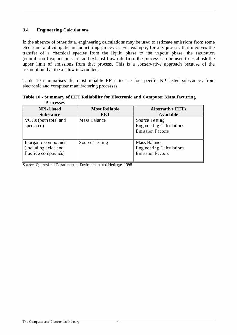
In the absence of other data, engineering calculations may be used to estimate emissions from someelectronic and computer manufacturing processes. For example, for any process that involves thetransfer of a chemical species from the liquid phase to the vapour phase, the saturation(equilibrium) vapour pressure and exhaust flow rate from the process can be used to establish theupper limit of emissions from that process. This is a conservative approach because of theassumption that the airflow is saturated.
Table 10 summarises the most reliable EETs to use for specific NPI-listed substances fromelectronic and computer manufacturing processes.
Table 10 - Summary of EET Reliability for Electronic and Computer Manufacturing ProcessesNPI-Listed Most Reliable Alternative EETsSubstance EET Available
VOCs (both total andspeciated)
Mass Balance Source TestingEngineering CalculationsEmission Factors
Inorganic compounds(including acids andfluoride compounds)
Source Testing Mass BalanceEngineering CalculationsEmission Factors
Source: Queensland Department of Environment and Heritage, 1998.
The Computer and Electronics Industry 26
4.0 Estimating Emissions
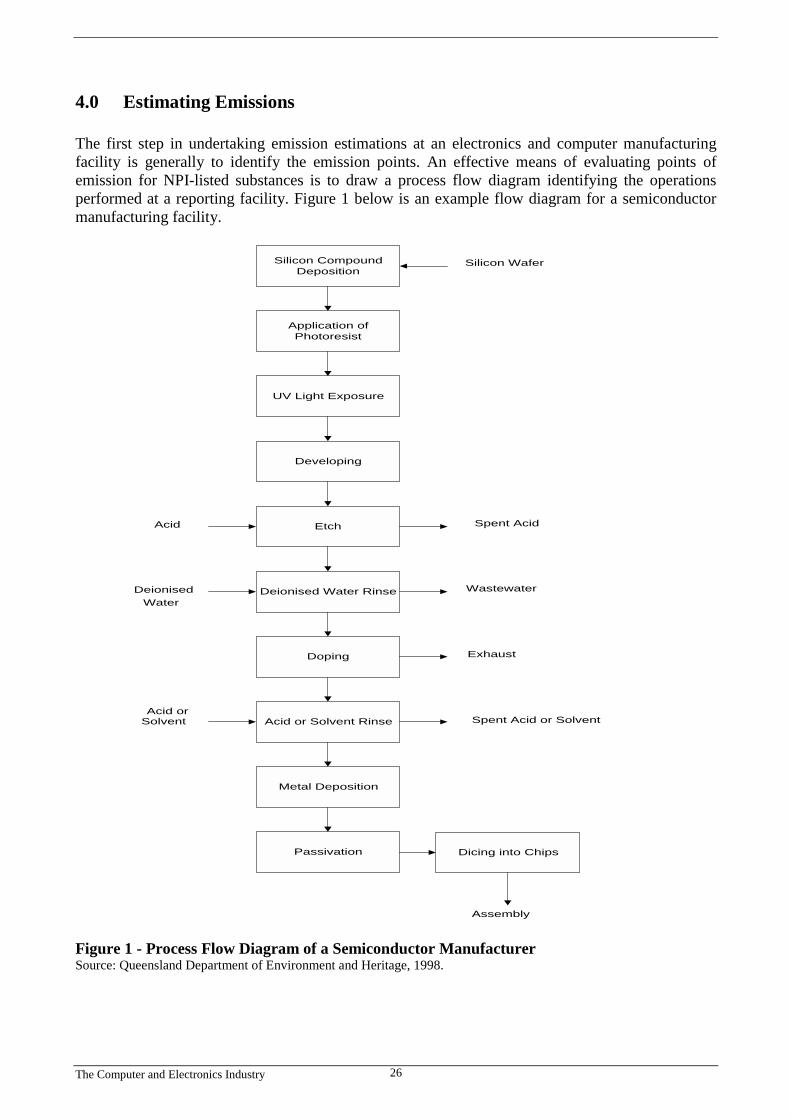
The first step in undertaking emission estimations at an electronics and computer manufacturingfacility is generally to identify the emission points. An effective means of evaluating points ofemission for NPI-listed substances is to draw a process flow diagram identifying the operationsperformed at a reporting facility. Figure 1 below is an example flow diagram for a semiconductormanufacturing facility.
Silicon CompoundDeposition
Application ofPhotoresist
UV Light Exposure
Developing
Etch
Deionised Water Rinse
Doping
Acid or Solvent Rinse
Metal Deposition
Dicing into ChipsPassivation
Silicon Wafer
Acid Spent Acid
DeionisedWater
Wastewater
Exhaust
Spent Acid or SolventAcid or
Solvent
Assembly
Figure 1 - Process Flow Diagram of a Semiconductor ManufacturerSource: Queensland Department of Environment and Heritage, 1998.
The Computer and Electronics Industry 27
Because each facility is unique, reporting facilities are strongly urged to develop flow diagrams fortheir own particular operations that detail the input of materials and chemicals and the emissionssources resulting from the operation of each unit.
Emissions to the atmosphere (to air), wastewater (to water), and via solid wastes (to land) are likelyto be the primary emission points to consider. If water is treated on-site, sludges or other wastescontaining listed substances may be created. Other emissions may come from discarded containersor samples, vessel washings, or, for some substances, volatilisation to the air. Facility operatorsshould ensure that all emissions are accounted for when reporting.
After all the NPI-listed substances and emission sources at the reporting facility have beenidentified, the procedures for estimating emissions, of EETs, can proceed. The usual approachentails first estimating emissions from emission sources across a facility for all substancestriggering a threshold and then, based on the disposal method used, determining whether emissionsfrom a particular emission source are to air, water, land, or an off-site disposal facility. (The off-sitetransfer of NPI-listed substances, including listed substances contained in wastes, does not requirereporting, but may nevertheless require characterisation and estimation if emissions are beingestimated from a mass balance).
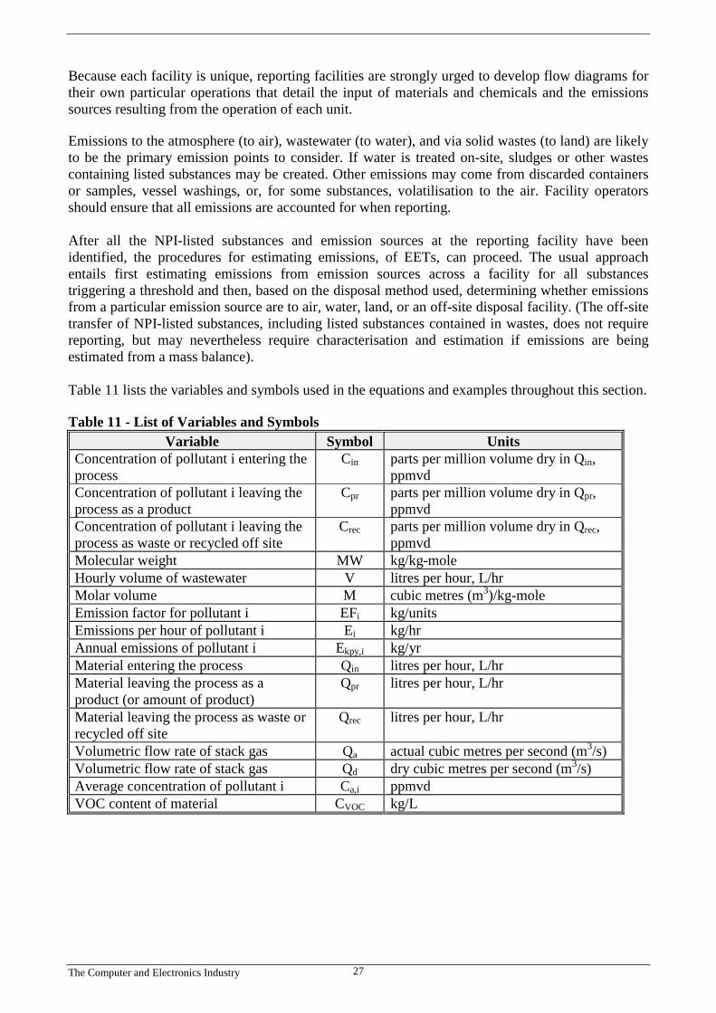
Table 11 lists the variables and symbols used in the equations and examples throughout this section.
Table 11 - List of Variables and SymbolsVariable Symbol Units
Concentration of pollutant i entering theprocess
Cin parts per million volume dry in Qin,ppmvd
Concentration of pollutant i leaving theprocess as a product
Cpr parts per million volume dry in Qpr,ppmvd
Concentration of pollutant i leaving theprocess as waste or recycled off site
Crec parts per million volume dry in Qrec,ppmvd
Molecular weight MW kg/kg-moleHourly volume of wastewater V litres per hour, L/hrMolar volume M cubic metres (m3)/kg-moleEmission factor for pollutant i EFi kg/unitsEmissions per hour of pollutant i Ei kg/hrAnnual emissions of pollutant i Ekpy,i kg/yrMaterial entering the process Qin litres per hour, L/hrMaterial leaving the process as aproduct (or amount of product)
Qpr litres per hour, L/hr
Material leaving the process as waste orrecycled off site
Qrec litres per hour, L/hr
Volumetric flow rate of stack gas Qa actual cubic metres per second (m3/s)Volumetric flow rate of stack gas Qd dry cubic metres per second (m3/s)Average concentration of pollutant i Ca,i ppmvdVOC content of material CVOC kg/L
The Computer and Electronics Industry 28
Table 11 - List of Variables and Symbols (cont’)Variable Symbol Units
Percentage by weight of pollutant i inmaterial
wt% %
Temperature correction for differencesin temperature during test
Kt dimensionless
Pressure correction for differences inpressure during test
Kp dimensionless
Activity rate A units/hrSaturation vapour pressure of pollutant i Psat,i kilopascals, kPaTotal pressure Pt kPaDensity of pollutant i (or vapour densityof pollutant i )
ρi kg/m3
Density of material ρm kg/LEvaporation rate of pollutant i Wkpy,i kg/yrGas-phase mass transfer coefficient forVOC species i
Ki m/sec
Surface area area m2
Vapour pressure of pollutant i Pvap,i kPaUniversal gas constant R 8.314 kPa * m3/(kgmol * K)Metered volume at standard temperatureand pressure
Vm, STP m3
Wind speed U km/hrTemperature T oCelsius, specify °C (or if necessary
Kelvin, ie. absolute temperature, K) ineach equation
Annual operating hours OpHrs hours/yearSource: Queensland Department of Environment and Heritage, 1998.
4.1 Using Mass Balance
4.1.1 Estimating Emissions to Air
Mass balance is the recommended EET for estimating emissions of total VOCs and speciatedorganics in solvents, etchants, and cleaners. Total VOC emissions from electronic and computermanufacturing facilities may be estimated by application of Equation 1 where the pollutantconcentration is constant throughout the process.
Equation 1Ei = (Qin - Qout) * Ci
where:
Ei = total emissions of pollutant i, kg/hrQin = material entering the process, L/hrQout = material leaving the process as waste, recycled,
or in product, L/hrCi = concentration of pollutant i, kg/L
Example 1 illustrates the application of Equation 1.
Example 1 - Using a Mass Balance to Estimate VOC Emissions
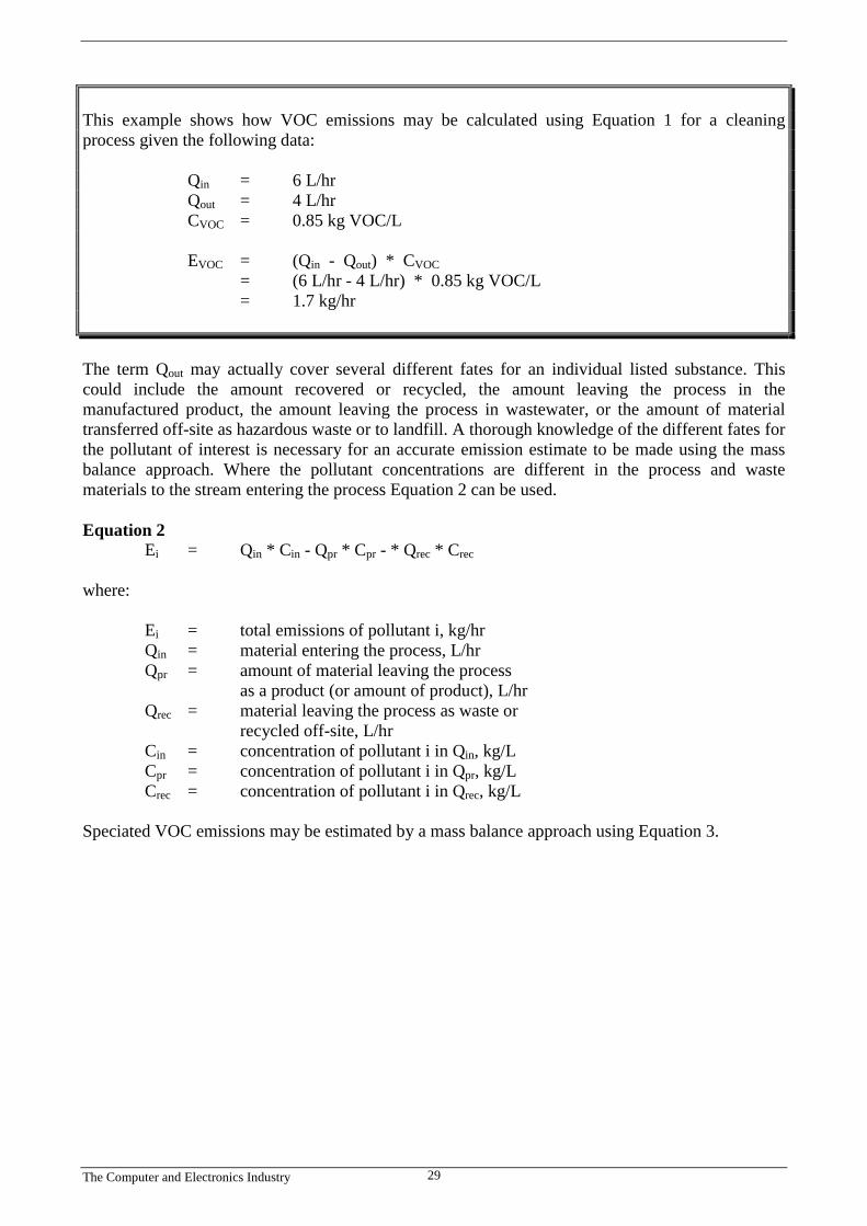
The Computer and Electronics Industry 29
This example shows how VOC emissions may be calculated using Equation 1 for a cleaningprocess given the following data:
Qin = 6 L/hrQout = 4 L/hrCVOC = 0.85 kg VOC/L
EVOC = (Qin - Qout) * CVOC= (6 L/hr - 4 L/hr) * 0.85 kg VOC/L= 1.7 kg/hr
The term Qout may actually cover several different fates for an individual listed substance. Thiscould include the amount recovered or recycled, the amount leaving the process in themanufactured product, the amount leaving the process in wastewater, or the amount of materialtransferred off-site as hazardous waste or to landfill. A thorough knowledge of the different fates forthe pollutant of interest is necessary for an accurate emission estimate to be made using the massbalance approach. Where the pollutant concentrations are different in the process and wastematerials to the stream entering the process Equation 2 can be used.
Equation 2Ei = Qin * Cin - Qpr * Cpr - * Qrec * Crec
where:
Ei = total emissions of pollutant i, kg/hrQin = material entering the process, L/hrQpr = amount of material leaving the process
as a product (or amount of product), L/hrQrec = material leaving the process as waste or
recycled off-site, L/hrCin = concentration of pollutant i in Qin, kg/LCpr = concentration of pollutant i in Qpr, kg/LCrec = concentration of pollutant i in Qrec, kg/L
Speciated VOC emissions may be estimated by a mass balance approach using Equation 3.
The Computer and Electronics Industry 30
Equation 3Ei = (Qin - Qout) * ρm * (wt%i) /100
where:
Ei = total emissions of pollutant i, kg/hrQin = material entering the process, L/hrQout = material leaving the process as a transfer, or as an article
or product, L/hrρm = density of material, kg/Lwt%i = percentage by weight of pollutant i in material, %
The use of Equation 3 should provide a reasonably accurate estimate in most cases, especially ifother emissions are small compared with air emission losses. Individual emissions of organicchemicals from storage tanks should be estimated using the methods and procedures outlined in theFuel and Organic Liquid Storage EET Manual.
Example 2 illustrates the application of Equation 3.
Example 2 - Using a Mass Balance to Speciate VOC Emissions
This example shows how toluene emissions may be calculated using Equation 3 for a cleaningprocess using toluene-containing solvent given the following data:
Qin = 6 L/hrQout = 4 L/hrρsolvent = 0.87 kg /Lwt%toluene = 25%
Etoluene = (Qin - Qout) * dsolvent * (wt%toluene / 100)= (6 L/hr - 4 L/hr) * 0.87 kg /L * (25/100)= 0.435 kg/hr
4.1.2 Estimating Emissions to Water
If no wastewater monitoring data exists, emissions to process water can be calculated based on amass balance of the process, shown by Equation 4.
Equation 4Ekpy,i = (Qin - Qout)
where:
Ekpy,i = emissions of pollutant i, kg/yrQin = amount of pollutant i used, kg/yrQout = amount of pollutant i incorporated into product + treated
on-site + transferred off-site in the reporting year, kg/yr
Where a facility uses a listed mineral acid or base, with this acid or base being effectivelyneutralised in use or during wastewater treatment (to a pH of 6 to 8, as required by most State and
The Computer and Electronics Industry 31
Territory effluent standards), no emission quantities should be reported. If the acid or base is itselftransformed into another listed substance, however, the quantity of this substance coincidentallyproduced must be determined to assess if a threshold value has been reached. For example, sulfuricacid often yields hydrogen sulfide (an NPI-listed substance) in effluent streams.
4.1.3 Estimating Emissions to Land
Wastewater treatment may transport the reportable substance to a sludge. Facilities are oftenrequired to obtain data on the concentration of metals and other substances in sludges as part oftheir licensing requirement and this data can be used to calculate the emissions as kilograms ofsludge times concentrations of the substance in the sludge. Alternatively, the loss in the sludge canbe estimated by application of Equation 5. Although listed substances in sludge transferred off-sitefor waste disposal/treatment do not require reporting, determining this loss may be a necessary stepin the application of such a mass balance approach.
Equation 5ASkpy,i = (PLi - WLi ) * OpHrs
where:
ASkpy,i = amount of pollutant i in sludge, kg/yrPLi = process losses of pollutant i, kg/hrWLi = losses of pollutant i in wastewater, kg/hrOpHrs = operational hours, hr/yr
For many listed substances used and emitted during chemical processes, some degradation intreatment may occur so not all of the substance is transferred to the sludge. Facilities can estimatethe amount of reportable compounds in the sludge by using measured data, or by subtracting theamount biodegraded from the total amount removed in treatment. The amount of removal can bedetermined from operating data, and the extent of biodegradation might be obtained from publishedstudies. If the biodegradability of the chemical cannot be measured or is not known, reportingfacilities should assume that all removal is due to absorption to sludge.
4.2 Using Sampling Data
4.2.1 Estimating Emissions to Air
Sampling test methods can be used to estimate organic and inorganic pollutant emission rates fromsemiconductor and other electronic manufacturing processes. Airflow rates can be determined fromflow rate metres or from pressure drops across a critical orifice (an opening).
Sampling test reports often provide chemical concentration data in parts per million by volume(ppmv). If the concentration is known, an hourly emission rate can be determined using Equation 6.
Equation 6 Ei = (Ci * MWi * Qd * 3600) / [22.4 * {(T + 273)/273} * 106]
where: Ei = total emissions of pollutant i, kg/hr
The Computer and Electronics Industry 32
Ci = concentration of pollutant i, ppmv (volume of pollutant gas/106
volumes of dry air) MWi = molecular weight of pollutant i, kg/kg-mole Qd = stack gas volumetric flow rate, m3 /s 22.4 = volume occupied by 1 mole of ideal gas at standard temperature and pressure (0°C and 101.3 kPa), m3/kg-mole 3 600 = conversion factor, s/hr T = temperature of gas sample, °C
106 = conversion factor from ppmv to volume fraction
Emissions in kilograms per year can be calculated by multiplying the average hourly emission rate(kg/hr) from Equation 6 by the number of operating hours (shown in Equation 7 below) or bymultiplying an average emission factor (kg/L) by the total annual amount of material used (L).
Equation 7Ekpy,i = Ei * OpHrs
where:
Ekpy,i = annual emissions of pollutant i, kg/yrEi = total hourly emissions of pollutant i, kg/hrOpHrs = annual operating hours, hr/yr
Concentration data obtained from source testing may come in a variety of units, including parts permillion volume (ppmv), or grams per cubic metre (g/m3), and in a variety of conditions, such aswet, dry, or excess O2. This may require conversion of concentration data to consistent units forcompatibility with the equations given above.
Example 3 illustrates the use of Equation 6, and Equation 7.
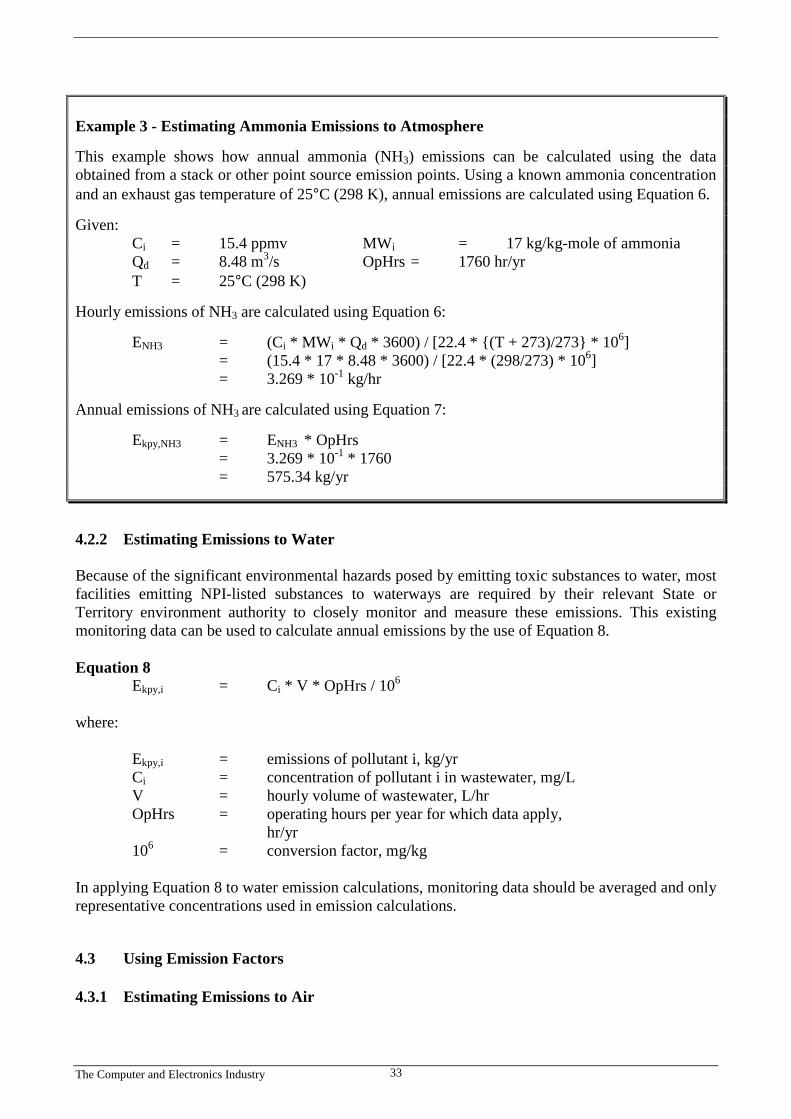
The Computer and Electronics Industry 33
Example 3 - Estimating Ammonia Emissions to Atmosphere This example shows how annual ammonia (NH3) emissions can be calculated using the dataobtained from a stack or other point source emission points. Using a known ammonia concentrationand an exhaust gas temperature of 25°C (298 K), annual emissions are calculated using Equation 6. Given: Ci = 15.4 ppmv MWi = 17 kg/kg-mole of ammonia Qd = 8.48 m3/s OpHrs = 1760 hr/yr T = 25°C (298 K) Hourly emissions of NH3 are calculated using Equation 6: ENH3 = (Ci * MWi * Qd * 3600) / [22.4 * {(T + 273)/273} * 106]
= (15.4 * 17 * 8.48 * 3600) / [22.4 * (298/273) * 106] = 3.269 * 10-1 kg/hr
Annual emissions of NH3 are calculated using Equation 7: Ekpy,NH3 = ENH3 * OpHrs = 3.269 * 10-1 * 1760
= 575.34 kg/yr
4.2.2 Estimating Emissions to Water
Because of the significant environmental hazards posed by emitting toxic substances to water, mostfacilities emitting NPI-listed substances to waterways are required by their relevant State orTerritory environment authority to closely monitor and measure these emissions. This existingmonitoring data can be used to calculate annual emissions by the use of Equation 8.
Equation 8Ekpy,i = Ci * V * OpHrs / 106
where:
Ekpy,i = emissions of pollutant i, kg/yrCi = concentration of pollutant i in wastewater, mg/LV = hourly volume of wastewater, L/hrOpHrs = operating hours per year for which data apply,
hr/yr106 = conversion factor, mg/kg
In applying Equation 8 to water emission calculations, monitoring data should be averaged and onlyrepresentative concentrations used in emission calculations.
4.3 Using Emission Factors
4.3.1 Estimating Emissions to Air
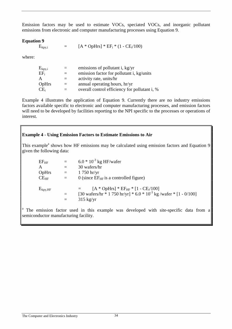
The Computer and Electronics Industry 34
Emission factors may be used to estimate VOCs, speciated VOCs, and inorganic pollutantemissions from electronic and computer manufacturing processes using Equation 9.
Equation 9Ekpy,i = [A * OpHrs] * EFi * (1 - CEi/100)
where:
Ekpy,i = emissions of pollutant i, kg/yrEFi = emission factor for pollutant i, kg/unitsA = activity rate, units/hrOpHrs = annual operating hours, hr/yrCEi = overall control efficiency for pollutant i, %
Example 4 illustrates the application of Equation 9. Currently there are no industry emissionsfactors available specific to electronic and computer manufacturing processes, and emission factorswill need to be developed by facilities reporting to the NPI specific to the processes or operations ofinterest.
Example 4 - Using Emission Factors to Estimate Emissions to Air
This examplea shows how HF emissions may be calculated using emission factors and Equation 9given the following data:
EFHF = 6.0 * 10-3 kg HF/waferA = 30 wafers/hrOpHrs = 1 750 hr/yrCEHF = 0 (since EFHF is a controlled figure)
Ekpy,HF = [A * OpHrs] * EFHF * [1 - CEi/100]= [30 wafers/hr * 1 750 hr/yr] * 6.0 * 10-3 kg /wafer * [1 - 0/100]= 315 kg/yr
a The emission factor used in this example was developed with site-specific data from asemiconductor manufacturing facility.
The Computer and Electronics Industry 35
4.3.2 Estimating Emissions to Water
Table 12 gives minimum and maximum concentrations for many NPI-listed substances contained inuntreated wastewaters from US semiconductor facilities. In the absence of site-specific monitoringdata, this US data can be used as emission factors to estimate emissions to wastewater. Equation 10shows this calculation.
Equation 10Ekpy,i = Ci * V * OpHrs/106 * [1 - (CEi/100)]
where:Ekpy,i = emissions of pollutant i, kg/yrCi = concentration of pollutant i in wastewater, mg/LV = hourly volume of wastewater, L/hr106 = conversion factor, mg/kgCEi = overall emission control efficiency of the wastewater
treatment operation for pollutant i, %
Where wastewaters are treated on-site, emissions must be adjusted to reflect the effectiveness of thetreatment. Where available, data on the operation of the specific treatment facility should be used.Example 5 illustrates the application of Equation 10 showing how to adjust an emission factorequation to take account of the control efficiency of a wastewater treatment operation.
Example 5 - Using Emission Factors to Estimate Emissions to Water
Using published wastewater emission concentrations, annual wastewater emissions of chloroformcan be calculated using Equation 10 and the maximum concentration reported from untreatedwastewater (from Table 12). Assume the facility operates for 260 days during year, an average 4000 000 litres of water is used daily, and the facility’s wastewater treatment plant has an efficiencyfor chloroform of 87% following screening and trickling filter.
Ekpy,chloroform = Ci * V * OpHrs/106 * [1 - (CEi/100)]
Ekpy,chloroform = 2.6 mg/L * 4 000 000 L/day * 260 day/yr/106 mg/kg * [1 - (87/100)]
= 351.5 kg/yr
The Computer and Electronics Industry 36
Table 12 - Concentration of NPI-Listed Substances in Untreated Wastewater from US Semiconductor Manufacturing Facilities
NPI-Listed SubstanceMinimum
Concentration(mg/L)
MaximumConcentration
(mg/L)Benzene < 0.01 0.190Chloroform 0.004 2.6Dichloromethane (methylene chloride) 0.005 2.4Phenol 0.0004 5.7Bis(2-ethylhexyl)phthalate 0.002 0.750Ethylbenzene 0.0002 0.107Tetrachloroethylene (perchloroethylene) 0.0002 0.80Toluene 0.0002 0.14Trichloroethylene 0.0049 3.5Antimony < 0.0005 0.187Arsenic < 0.003 0.067Beryllium < 0.001 < 0.015Cadmium < 0.001 0.008Chromium (total) < 0.001 1.150Cobalt < 0.001 0.48Copper < 0.005 2.588Cyanide < 0.005 0.01Lead < 0.04 1.459Manganese < 0.001 0.209Mercury < 0.001 0.051Nickel 0.005 4.964Selenium < 0.002 0.045Zinc 0.001 0.289
Source: USEPA AP-42, 1988.
4.4 Using Engineering Calculations
Theoretical and complex equations or models can be used for estimating emissions from electronicand computer manufacturing processes. Inputs for theoretical equations generally fall into thefollowing categories:
(1) chemical/physical properties of the material involved, such as vapour pressure and vapourmolecular weight;
(2) operating data, such as the amount of material processed and operating hours; and(3) physical characteristics and properties of the source, such as tank colour and diameter.
Engineering equations are suitable for estimating emissions from several chemical manufacturingprocesses. For example, for any process involving a transfer of a chemical species from the liquidphase to the vapour phase, the saturation or equilibrium vapour pressure and exhaust flow rate fromthe process can be used to establish the upper limit of emissions from that particular process. This isa conservative approach because of the assumption that the total airflow is saturated. An alternativetechnique based on mass transfer kinetics does not assume airflow saturation and results in a loweremission rate estimate than would be obtained assuming saturation.
4.4.1 Estimating Emissions Using Mass Transfer Kinetics
An EET based on mass transfer kinetics is shown by Equation 11.
The Computer and Electronics Industry 37
Equation 11Ekpy,i = (MWi * Ki * area * Pvap,i * 3600 * OpHrs) / (R * T)
where:
Ekpy,i = emission (evaporation rate) of pollutant i, kg/yrMWi = molecular weight of pollutant i, kg/kg-moleKi = gas-phase mass transfer coefficient for VOC
species i, m/sec= [0.00438 * (0.62138 * U)0.78 * (18/MWi)1/3]/3.2808
U = wind speed, km/hrarea = surface area, m2
Pvap,i = vapour pressure of pollutant i, kPa3600 = conversion of 3600 sec/hrOpHrs = hours of operation each year hr/yrR = universal gas constant (8.314 kPa * m3 /(kg-mol * K))T = temperature, K
Example 6 illustrates the application of this equation.
Example 6 - Using Mass Transfer Kinetics
This example shows how methanol emissions may be estimated using mass transfer kinetics andEquation 11 given the following data:
MWmethanol = 32 kg/kg-moleU = 7.24 km/hrarea = 0.6 m2
Pvap,methanol = 13.16 kPa3600 = 3600 sec/hrOpHrs = 1000 hr/yrT = 296 KR = 8.314 kPa * m3 /(kg-mol * K)
First, calculate the mass transfer coefficient, Ki:
Ki = [0.00438 * (0.62138 * U)0.78 * (18/MWi)1/3]/3.2808= [0.00438 * (0.62138 * 7.24 km/hr)0.78 * (18/32 kg/kg-
mole)1/3/3.2808]= 0.0035 m/s
Then, calculate Ekpy,methanol:
Ekpy,methanol = (MWmethanol * Ki * area * Pvap,methanol * 3600 * OpHrs) / (R * T)= (32 kg/kg-mole * 0.0035 m/sec * 0.6 m2 * 13.16 kPa * 3600
sec/hr * 1000 hr/yr)/{(8.314 kPa * m3/(kg-mol * K)) * (296 K)}= 1294 kg/yr
4.4.2 Estimating Emissions from Spills A vaporisation equation can be used to estimate the evaporation rate of a liquid chemical spill if thesize area of the spill is known or can be estimated. This is illustrated by Equation 12.
The Computer and Electronics Industry 38
Equation 12 Ei = (MWi* Ki* area * Pi* 3 600 * HR) / (R * T) where: Ei = emissions of VOC species i from the spill, kg/event MWi = molecular weight of VOC species i, kg/kg-mole Ki = gas-phase mass transfer coefficient for VOC species i,
m/sec area = surface area of spill, m2
Pi = partial pressure of VOC species i (if a pure chemical is spilled) or the partial pressure of chemical i (if a mixture
of VOCs is spilled) at temperature T, kPa; the partial pressure of VOC species i (Pi) may be calculated using Equation 13 or Equation 14
3 600 = conversion factor, sec/hr HR = duration of spill, hr/event R = universal gas constant at 101.3 kPa of pressure, (8.314 kPa * m3/ (kg-mol * K) T = temperature of the liquid spilled, K Pi may be calculated using Raoult’s Law (for ideal solutions) or Henry’s Law constants (whengases are dissolved at low concentrations in water). Raoult’s Law is given in Equation 13. Equation 13 Pi = mi * VPi where: Pi = partial vapour pressure of VOC species i, kPa mi = liquid mole fraction of VOC species i, mole/mole VPi = true vapour pressure of VOC species i, kPa Pi may be calculated using Henry’s Law constants and Equation 14. Equation 14 Pi = mi * Hi where: Pi = partial vapour pressure of VOC species i, kPa mi = liquid mole fraction of VOC species i, mole/mole Hi = Henry’s Law constant for VOC species i, kPa The gas-phase mass transfer coefficient (Ki) may be calculated using Equation 15. Equation 15 Ki = [0.00438 * (0.62138 * U)0.78 * (Di/0.288)2/3]/3.2808 where: Ki = gas-phase mass transfer coefficient for VOC species i,
m/sec
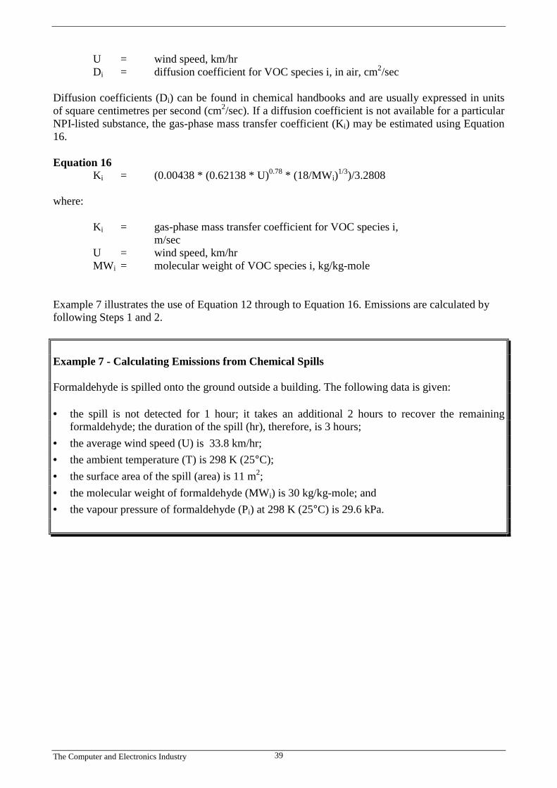
The Computer and Electronics Industry 39
U = wind speed, km/hr Di = diffusion coefficient for VOC species i, in air, cm2/sec Diffusion coefficients (Di) can be found in chemical handbooks and are usually expressed in unitsof square centimetres per second (cm2/sec). If a diffusion coefficient is not available for a particularNPI-listed substance, the gas-phase mass transfer coefficient (Ki) may be estimated using Equation16. Equation 16 Ki = (0.00438 * (0.62138 * U)0.78 * (18/MWi)1/3)/3.2808 where: Ki = gas-phase mass transfer coefficient for VOC species i,
m/sec U = wind speed, km/hr MWi = molecular weight of VOC species i, kg/kg-mole Example 7 illustrates the use of Equation 12 through to Equation 16. Emissions are calculated byfollowing Steps 1 and 2.
Example 7 - Calculating Emissions from Chemical Spills Formaldehyde is spilled onto the ground outside a building. The following data is given: • the spill is not detected for 1 hour; it takes an additional 2 hours to recover the remaining
formaldehyde; the duration of the spill (hr), therefore, is 3 hours;• the average wind speed (U) is 33.8 km/hr;• the ambient temperature (T) is 298 K (25°C);• the surface area of the spill (area) is 11 m2;• the molecular weight of formaldehyde (MWi) is 30 kg/kg-mole; and• the vapour pressure of formaldehyde (Pi) at 298 K (25°C) is 29.6 kPa.
The Computer and Electronics Industry 40
Step 1: Using Equation 16, Calculate the Gas-Phase Mass Transfer Coefficient(Kformaldehyde) Kformaldehyde = (0.00438 * (0.62138 * U)0.78 * (18/MWi)1/3)/3.2808 = (0.00438 * (0.62138 * 33.8)0.78 * (18/30)1/3)/3.2808 = 0.0124 m/sec Step 2: Using Equation 12, Calculate Emissions (Eformaldehyde) Eformaldehyde = (MWi * Ki * area * Pi * 3 600 * HR) / (R * T) = (30 * 0.0124 * 11 * 29.6 * 3 600 * 3) / (8.314 * 298) = 528 kg/spill
4.4.3 Estimating Fugitive Emissions
Many of the engineering equations presented in this section are to be applied to estimate emissionsof organic compounds. Other than using emission factors or applying the mass balance techniquefor estimating emissions, there is little information currently available for estimating fugitiveemissions of inorganic compounds. However, in electronics and computer manufacturing, it may benecessary to estimate emissions of inorganic compounds for NPI-reporting purposes. This isparticularly the case for mineral acids in the gas/vapour phase.
Emission estimates of inorganic compounds can be obtained for electronics and computermanufacturing processes by the following techniques:
• develop correlations specific to particular chemical manufacturing processes;• use a portable monitoring instrument to obtain actual concentrations of the inorganic compounds
and then apply the screening values obtained (see paragraph below) into the applicablecorrelation equation shown in Table 13 and Equation 17; or
• Use the screening values obtained above and apply the emission factors, from Table 14,corresponding to the screening range obtained.
Screening data is collected by using a portable monitoring instrument to sample air from potentialleak interfaces on individual pieces of equipment. A screening value (SV) is a measure of theconcentration of leaking compounds in the ambient air that provides an indication of the leak ratefrom an equipment piece, and is measured in units of parts per million by volume (ppmv).
Also, surrogate measurements can be used to estimate emissions of inorganic compounds. Forexample, potassium iodide (KI), or a similar salt solution, is an indicator for equipment leaks fromacid process lines. Equation 17 illustrates an approach for estimating fugitive inorganic chemicalemissions using data from Table 13.
The Computer and Electronics Industry 41
Equation 17Ekpy,i = ERi * Ci/100* OpHrs * number of sources
where:
Ekpy,i = mass emissions of pollutant i calculated from either the screening values, correlation equation,
or emission factors, kg/yr/sourceERi = emission rate, kg/hr/sourceCi = concentration of pollutant i in the equipment, %OpHrs = operating hours, hr/yr/source
The application of Equation 17 is given at Example 8.
Table 13 - Correlation Equations, Default Zero Emission Rates, and Peggedc Emission Rates for Estimating Fugitive Emissions
EquipmentDefault
Zero EmissionPegged Emission Rates
(kg/hr per source) Correlation EquationType Rate
(kg/hr/source)10 000 ppmv 100 000 ppmv (kg/hr per source) a
Gas valves 6.6 * 10-7 0.024 0.11 LR = 1.87 * 10-6 *(SV)0.873
Light liquid valves 4.9 * 10-7 0.036 0.15 LR = 6.41 * 10-6 *(SV)0.797
Light liquid pumpsb 7.5 * 10-6 0.14 0.62 LR = 1.90 * 10-5 *(SV)0.824
Connectors 6.1 * 10-7 0.044 0.22 LR = 3.05 * 10-6 *(SV)0.885
Source: Eastern Research Group, 1996.LR = leak rate.a SV is the screening value (ppmv) measured by the monitoring device. To estimate emissions, use the default zero
emission rates only when the screening value (adjusted for background) equals 0.0 ppmv; otherwise use thecorrelation equations. If the monitoring device registers a pegged value, use the appropriate pegged emission rate.
b The emission estimates for light liquid pump seals can be applied to compressor seals, pressure relief valves, agitatorseals, and heavy liquid pumps.
c When the monitoring device reads a pegged value; for example 10 ppmv for a gas valve, the pegged emission rate of0.024 kg/hr per source would be used rather than determining the emission rate using a correlation equation, or adefault zero emission rate.
The Computer and Electronics Industry 42
Example 8 - Estimating Fugitive Emissions
A electronics manufacturing facility operates a light-liquid pump on an 80 percent ammoniasolution storage tank. The pump is run for 8760 hours during the year.
For a Screening Value of zero ppmv
OpHrs = 8760 hr/yrSV (screening value) = 0 ppmvDefault-zero emission rate = 7.5 * 10-6 kg/hr/source
Using Equation 17:NH3 emissions = ERi * Ci/100* OpHrs * number of sources
= 7.5 * 10-6 kg/hr/source * (80/100) * 8760 hr/yr
= 5.26 * 10-2 kg/yr
For a Screening Value of 20 ppmv
OpHrs = 8760 hr/yrSV (screening value)= 20 ppmv
NH3 emissions (kg/hr) = 1.90 * 10-5 (SV)0.824
= 1.90 * 10-5 (20)0.824
= 2.24 * 10-4 kg/hr
NH3 emissions (kg/yr) = 2.24 * 10-4 kg/hr * 8760 hr/yr * (80/100)
= 1.57 kg/yr
Table 14 - Emission Factors for Equipment LeaksEquipment Type Service Emission Factor
(kg/hr/source)Valves Gas 0.00597
Light liquid 0.00403Heavy liquid 0.00023
Pump seals a Light liquid 0.0199Heavy liquid 0.00862
Compressor seals Gas 0.228Pressure relief valves Gas 0104Connectors All 0.00183Open-ended lines All 0.0017Sampling connections All 0.0150
Source: Eastern Research Group, 1996.a The light liquid pump seal factor can be used to estimate the leak rate from agitator seals.
4.5 Other Emission Sources
The Computer and Electronics Industry 43
As shown in earlier sections, electronic and computer manufacturing activities produce otheremission sources for NPI-listed substances. These include:
• residues from pollution control devices;• wash and rinse water from equipment cleaning;• product rejects;• used equipment; and• empty chemical containers.
Emissions from these sources may already have been accounted for, depending on the emissionestimation techniques used. These items (and others of a similar facility specific nature) should beincluded in the development of a process flow diagram.
The contribution of the above sources of emissions, such as cleaning out vessels or discardingcontainers, should be small when compared with process losses. If data is unavailable for thesesources (or any monitoring data on overall water emissions), facility operators should assume up to1 percent of total vessel content may be lost during each cleaning occurrence. For example, if afacility discards the empty drums that have not been cleaned, calculate the emission as 1 percent ofnormal drum content. If the drum is transferred off-site to a landfill or to a drum recycler, then thereportable substance is also transferred off-site and therefore does not require reporting. If however,the drums are washed before disposal, this may contribute 1 percent of the content to the facility’swastewater loading.
The Computer and Electronics Industry 44
5.0 References
Flatt, Michael, 1992, Printed Circuit Board Basics: Quick and Easy Guide, 2nd Ed.
USEPA, January 1988, Title II Section 313 Release Reporting Guidance: Estimating ChemicalReleases from Semiconductor Manufacturing. United States Environmental Protection Agency,Office of Pesticides and Toxic Substances, Washington, DC, USA.
USEPA, 1994, Toxic Release Inventory (TRI) Public Data Release 1993. United StatesEnvironmental Protection Agency, Office of Pollution Prevention and Toxics, (EPA/745-R94-001),Washington, DC, USA.
USEPA, October 1992, VOC / PM Speciation Data System - Version 1.50. United StatesEnvironmental Protection Agency, Office of Air Quality Planning and Standards, ResearchTriangle Park, NC, USA.
USEPA, September 1995, EPA Office of Compliance Sector Notebook Project. Profile of theComputer and Electronics Industry, United States Environmental Protection Agency, Office ofEnforcement and Compliance Assurance, Washington, DC, USA.
Van Zant, Peter, 1990, Microchip Fabrication: A Practical Guide to Semiconductor Processing,2nd Ed. McGraw Hill, Inc.
The following Emission Estimation Technique Manual referred to in this Manual is available at theNPI Homepage (http://www.npi.gov.au) and from your local environmental protection agency (see thefront of the NPI Guide for details):
• Emission Estimation Technique Manual for Fuel & Organic Liquid Storage.