Embed Size (px)
Citation preview

Emílio Sérgio Marins Vieira Pinto
maio 2014
UM
inho
|201
4
Células solares e sensores de filme fino desilício depositados sobre substratos flexíveis
Cé
lula
s so
lare
s e
se
nso
res
de
film
e f
ino
de
silí
cio
de
po
sita
do
s so
bre
su
bst
rato
s fl
exív
eis
Emíli
o Sé
rgio
Mar
ins
Viei
ra P
into
Universidade do Minho
Escola de Ciências
Governo da República Portuguesa Fundo Social Europeu

maio 2014
Trabalho realizado sob a orientação do
Doutor João Pedro dos Santos Hall Agorreta Alpuim
Emílio Sérgio Marins Vieira Pinto
Células solares e sensores de filme fino desilício depositados sobre substratos flexíveis
Programa Doutoral em Física (MAP-fis)
Universidade do Minho
Escola de Ciências
DECLARAÇÃO
Nome
Emílio Sérgio Marins Vieira Pinto
Endereço electrónico: [email protected]
Título:
Células solares e sensores de filme fino de silício depositados sobre substratos flexíveis
Orientador(es):
Doutor João Pedro dos Santos Hall Agorreta Alpuim
Ano de conclusão: 2014
Designação do Doutoramento:
Doutoramento em Física
É AUTORIZADA A REPRODUÇÃO INTEGRAL DESTA TESE APENAS PARA EFEITOS DE INVESTIGAÇÃO, MEDIANTE DECLARAÇÃO ESCRITA DO INTERESSADO, QUE A TAL SE COMPROMETE;
Universidade do Minho, 16/05/2014 Assinatura: ________________________________________________


iii
Acknowledgements
First of all I thank my supervisor, Professor Pedro Alpuim, for the opportunity to do
my PhD work in his group. I am very grateful for everything I have learned with him
during the daily work and for his unflagging attitude to keep me motivated. More than
that, his example of dedication to the work, discipline, competence and enthusiasm are
things that I will take with me for my whole life!
I also thank Dr. Friedhelm Finger for the opportunity to complete this research at
Forschungszentrum Jülich (IEK-5), where, besides enjoying the pleasant and
cooperative work atmosphere, I have learned intensively under his careful and
competent supervision.
I would like to thank all the colleagues and technicians that have helped in this work,
at UM and IEK-5. Starting with the professors from the Department of Physics (UM):
Luís Rebouta, for the TCO depositions; Carlos Tavares, for allowing the transmittance
and reflectance measurements; Fátima Cerqueira, for the valuable help with the
measurements and analysis of Raman and transmittance spectroscopy and Senentxu
Lanceros-Mendez for supporting the characterization of the piezoresistive sensors. From
IEK-5 I would like to acknowledge A. Schmalen, J. Wolff, M. Hülsbeck and W. Reetz
for the technical support, A. Doumit, J. Worbs and H. Siekmann for the depositions of
the front and back contacts, and my colleagues Stephan Michard, Tao Chen and Marek
Warzecha for helping me with the depositions at CT2. Also, thanks to prof. Stefano
Chiussi and Stefan Stefanov, from University of Vigo, for the laser treatment of plastic
substrates.
To my friends from Jülich: Björn, Carolin, Damian, David, Elif, Etienne, Gaye,
Gokhan, Hang, Jonas, Jorj, Juri, Kaining, Lihong, Marek, Max, Olga, Sacha, Ümit,
Wanjiao, and all the others that I may have forgotten. Thank you all for the great
moments we had together! Your companionship and friendship have made my stay in
Jülich an unforgettable time!
Finally, thanks to my parents and sisters for all the support, love and encouragement,
which were always present during all these years, despite the physical distance.

iv

v
Título
“Células solares e sensores de filme fino de silício
depositados sobre substratos flexíveis”
Resumo
Células solares flexíveis de filmes finos de silício são geralmente fabricadas a baixa
temperatura sobre substratos de plástico ou a mais elevadas temperaturas sobre folhas
de aço. Esta tese reporta o estudo da deposição de filmes finos sobre diferentes
substratos de plástico, transparentes e coloridos, para células solares do tipo sobrestrato
e substrato, respectivamente. Como objetivo co-lateral, os filmes dopados depositados
sobre plástico foram usados como sensores de deformação, utilizando as suas
propriedades piezo-resistivas.
Elevadas taxas de deposição dos filmes de silício depositados sobre plástico foram
obtidas a baixa temperatura do substrato (150ºC) por rf-PECVD. A influência de
diferentes parâmetros de deposição sobre as propriedades e taxa de deposição dos filmes
resultantes foram estudados e correlacionados.
Células solares de filmes finos de silício amorfo e microcristalino foram
desenvolvidas a baixas temperaturas sobre plásticos. Eficiências de 5 – 6.5% foram
alcançadas para as células amorfas e 7.5% para as células microcristalinas. Efeitos de
aprisionamento da luz foram estudados através da texturização por ablação laser de
substratos de plástico e corrosão úmida de TCO sobre plástico.
Filmes finos de silício microcristalino, depositados por HW-CVD, com fator
piezoresistivo de -32.2, foram usados para fabricar sensores de deformação em uma
membrana plástica muito fina (15 µm). Estruturas de teste em têxtil e a miniaturização
dos sensores piezoresistivos depositados sobre substratos flexíveis de poliimida foram
abordados.

vi
vii
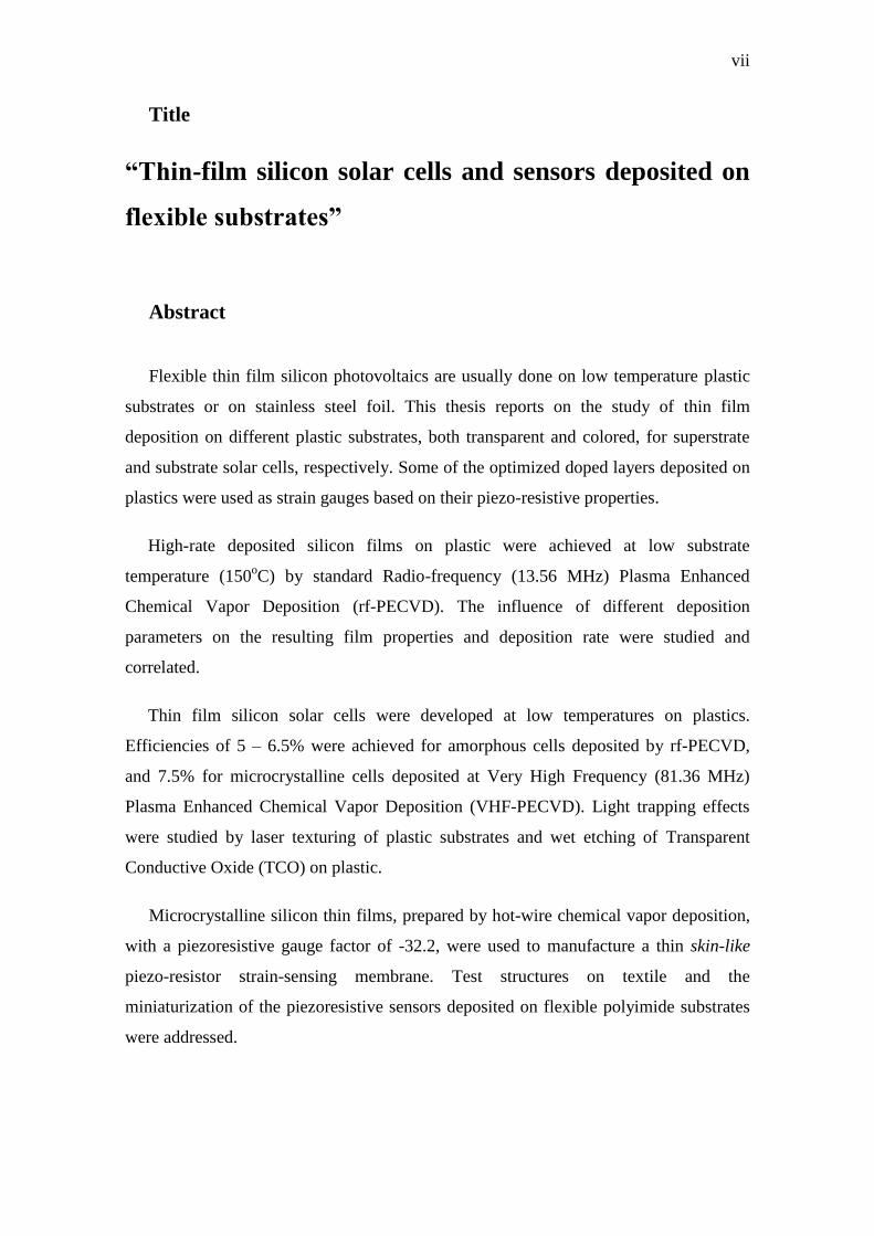
Title
“Thin-film silicon solar cells and sensors deposited on
flexible substrates”
Abstract
Flexible thin film silicon photovoltaics are usually done on low temperature plastic
substrates or on stainless steel foil. This thesis reports on the study of thin film
deposition on different plastic substrates, both transparent and colored, for superstrate
and substrate solar cells, respectively. Some of the optimized doped layers deposited on
plastics were used as strain gauges based on their piezo-resistive properties.
High-rate deposited silicon films on plastic were achieved at low substrate
temperature (150oC) by standard Radio-frequency (13.56 MHz) Plasma Enhanced
Chemical Vapor Deposition (rf-PECVD). The influence of different deposition
parameters on the resulting film properties and deposition rate were studied and
correlated.
Thin film silicon solar cells were developed at low temperatures on plastics.
Efficiencies of 5 – 6.5% were achieved for amorphous cells deposited by rf-PECVD,
and 7.5% for microcrystalline cells deposited at Very High Frequency (81.36 MHz)
Plasma Enhanced Chemical Vapor Deposition (VHF-PECVD). Light trapping effects
were studied by laser texturing of plastic substrates and wet etching of Transparent
Conductive Oxide (TCO) on plastic.
Microcrystalline silicon thin films, prepared by hot-wire chemical vapor deposition,
with a piezoresistive gauge factor of -32.2, were used to manufacture a thin skin-like
piezo-resistor strain-sensing membrane. Test structures on textile and the
miniaturization of the piezoresistive sensors deposited on flexible polyimide substrates
were addressed.

viii

ix
Contents
1 Introduction .............................................................................................................. 1
1.1 Photovoltaics and thin-film silicon solar cells ................................................... 1
1.2 Piezoresistive sensors ...................................................................................... 12
1.3 Plastic substrates .............................................................................................. 14
1.4 Organization of the thesis ................................................................................ 15
References ................................................................................................................. 18
2 Experimental Techniques ....................................................................................... 23
2.1 Plasma Enhanced Chemical Vapor Deposition ............................................... 23
2.2 Hot-Wire Chemical Vapor Deposition ............................................................ 30
2.3 CVD deposition systems ................................................................................. 34
2.4 Optical transmittance spectroscopy ................................................................. 38
2.5 Structural and chemical characterization ......................................................... 42
2.6 Electrical Material Characterization ................................................................ 44
2.7 Solar Cell Characterization .............................................................................. 48
2.8 Piezoresistance ................................................................................................ 51
References ................................................................................................................. 53
3 High-rate deposition of microcrystalline silicon thin films on plastics ................. 55
3.1 Introduction ..................................................................................................... 56
3.2 Experimental details ........................................................................................ 57
3.3 Structural properties ........................................................................................ 58
3.4 Deposition rate ................................................................................................. 60
3.5 Opto-electronic properties ............................................................................... 61
3.6 Doping ............................................................................................................. 63
3.7 Conclusions ..................................................................................................... 66
References ................................................................................................................. 67
4 Amorphous silicon solar cells on flexible substrates ............................................. 69

x
4.1 Introduction ..................................................................................................... 70
4.2 Experimental details ........................................................................................ 70
4.3 Doped ZnO films ............................................................................................. 72
4.4 p-i-n superstrate solar cells on PEN ................................................................ 74
4.5 n-i-p substrate solar cells on PI ....................................................................... 76
4.6 Laser texturing of PET substrates .................................................................... 78
4.7 Conclusions ..................................................................................................... 85
References ................................................................................................................. 86
5 Microcrystalline silicon solar cells on flexible PI substrate................................... 87
5.1 Introduction ..................................................................................................... 88
5.2 Experimental details ........................................................................................ 88
5.3 n-i-p solar cells on smooth PI substrate ........................................................... 90
5.4 n-i-p solar cells on PI with textured ZnO:Ga .................................................. 92
5.5 Conclusions ..................................................................................................... 94
References ................................................................................................................. 95
6 Shape sensors based on piezoresistive doped µc-Si:H ........................................... 97
6.1 Introduction ..................................................................................................... 98
6.2 Experimental details ........................................................................................ 99
6.3 skin-like piezoresistive sensing membranes .................................................. 103
6.4 Test structures for smart textiles .................................................................... 105
6.5 Sensor array fabrication ................................................................................. 108
6.6 Conclusions ................................................................................................... 109
References ............................................................................................................... 111
7 Conclusions .......................................................................................................... 113
7.1 High-rate deposition of silicon thin films on plastics .................................... 113
7.2 Flexible thin film silicon solar cells .............................................................. 114
7.3 Flexible µc-Si:H piezoresistive sensors ........................................................ 115
Chapter 1
1 Introduction
1.1 Photovoltaics and thin-film silicon solar cells
Photovoltaics (PV) is a fascinating field, that requires a multidisciplinary
understanding of the direct conversion of sunlight to electricity, the photovoltaic effect.
Photovoltaics, technically, holds the potential to fulfill the energy needs of humanity by
using only renewable solar energy, but it is also controversial and detractors have
argued that the manufacture of large-area low-cost semiconductor panels is virtually an
impossible task. They now appear to have been wrong, as solar PV electricity at a few
cents per kWh has proved to be a realistic target in sunny areas. This opens bright
perspectives for producing a substantial part of our electricity needs with PV [1].
The last decade has been particularly exciting for the field of photovoltaics, with the
global photovoltaic market growing at a dizzying pace. The production volume
increased every year by 40 to 70% over the last decade [2]. This strong growth was
stimulated by the perspective of short-term profit on markets with high feed-in tariffs;
but once these tariffs started to decrease, PV industry showed that manufacturing costs
could be decreased significantly year after year; the perception that green technologies
will play an increasingly important role in a society plagued by excessive consumption
of fossil fuels and faced with major climatic changes induced by human activity [1].
Until now, crystalline silicon (c-Si) PV technology, based on single crystal or
polycrystalline silicon wafers, has dominated the photovoltaic market, with 88 % of the
cell and module production in 2008 [2], and will probably continue to do so for several
more years. This technology has benefited indirectly from past research and investments
made by the semiconductor industry and, considered globally, it can be regarded as
robust and reliable. However, although the prices of polysilicon and silicon have
2 Chapter 1
dropped significantly in recent years, c-Si PV technology involves high energy and
labor inputs which make it difficult for any significant progress in reducing production
costs in the short term to occur [3]. Moreover, the growth of the crystalline silicon solar
cell industry was limited by the availability of the so-called “Si feedstock” or purified
polysilicon [4]. Indeed from 2005 onwards the PV industry has been using more
purified polysilicon than the semiconductor industry.
This lack of purified silicon was one of the important factors that opened up a
window of opportunity for thin-film PV technologies, which requires much less usage
of active material, as layers with thicknesses of only a few hundreds of nanometers or a
few micrometers are used, and the total number of processing steps is strongly reduced
compared to the full production chain for crystalline silicon. This gives the prospect of
very low production costs and significantly lower energy pay back times [5,6]. In
addition, the more aesthetic aspect of thin-film modules and the possibility of
manufacturing flexible, unbreakable modules, open up a full range of new PV solutions.
The major challenge of manufacturing low-cost thin-film solar modules has been the
up-scaling of lab processes to real “mass production” [1].
The “classical” thin-film PV technologies can be grouped in three large categories,
based on different active absorber materials: copper-indium-gallium-selenide (CIGS)
and variations thereof, cadmium telluride (CdTe) and, finally, hydrogenated amorphous
silicon (a-Si:H)/microcrystalline silicon (µc-Si:H) and their alloys.
Solutions based on the use of chalcopyrites (CIGS and derived compounds) are
attractive because of their record efficiencies achieved. They are, at the laboratory scale,
close to those of crystalline silicon. One of the major challenges is to control properly
the deposition of the quaternary alloy used as absorber material in a reproducible way
under mass production conditions. Also, for very large production volumes, indium
availability might become a concern. Cadmium telluride technology also benefits from
the medium to high efficiencies achieved at the laboratory scale and has the advantage
of the very fast and relatively “easy” deposition techniques used for the CdTe absorber.
Concerns about the availability of Te as well as acceptance issues linked to an intensive
use of a cadmium-containing compound could become critical factors for this
technology. Finally, thin-film silicon technologies (amorphous silicon, SiGe alloys,
microcrystalline silicon), even though they have not so far demonstrated similarly high
efficiencies at the laboratory scale, they do have the advantage of plentiful raw material
supply (Si and Sn or Zn in the simplest version of a single-junction solar cell with SnO2
Introduction 3
or ZnO contact layers), what is essential for a market size reaching several hundred GW
of PV modules annually. In such a context, thin-film silicon technology is currently the
only option sustainable in the long run among the proven thin-film PV technologies [7],
and will most likely play a key role, as it is today the only technology combining the
advantage of virtually infinite resources with low material usage. Other reasons for the
uniqueness of thin-film silicon are: (1) the basics are well established: this includes the
control of doping levels, as well as reproducible fabrication processes for depositing
device-quality layers; (2) no hazardous materials (such as Cd or Pb) are required in thin-
film silicon technology, making it, if not safer, at least free from acceptance problems
and/or regulatory risks; (3) the low temperature coefficient of down to -0.2 %/ºC and
the self-annealing effect of the amorphous silicon material should ensure that, for high
module operating temperatures, the annual energy yield is superior by 5 to 10 % when
compared to other types of thin-film or crystalline-silicon modules; finally, (4) a strong
synergy with another industrial sector, the flat panel display industry, is present [1].
As a technology, a-Si:H based device fabrication has already proved to be mature
enough to meet all industry demands. The history of thin-film silicon technology started
over 30 years ago, with the fabrication of the first thin-film silicon solar cell based on a-
Si:H [8]. Since then, research and development (R&D) efforts have led to single- and
multi-junction solar cells and large-area modules based on a-Si:H and related alloys.
The demonstration in the mid 90’s of a complete microcrystalline silicon cell made
by very high-frequency (VHF) plasma enhanced chemical vapour deposition (PECVD)
with an efficiency of 4.6% opened up a new area of photovoltaic development [9].
However, cell efficiencies were limited by low open circuit voltages and fill factors.
The main advantage of these cells is the stability to light soaking and a better long
wavelength response, when compared to a-Si:H cells. However, improvement in the
efficiency of the single junction and application as a bottom cell in a tandem concept – a
double junction consisting of a top a-Si:H cell and a bottom μc-Si:H cell – which
showed an initial efficiency of 13%, looked like a breakthrough in the low temperature
process [10]. A quick adaptation of this concept and its translation into industrial
production by Kaneka Corporation has established the technological viability of this
low temperature process. This rapid adaptation was possible due to the maturity of the
amorphous silicon technology, including the back reflector, the transparent conductive
oxide (TCO), monolithic integration and encapsulation.

4 Chapter 1
If the gases used for deposition of amorphous silicon are highly diluted in hydrogen,
the deposit consists of regions of crystalline silicon immersed in an amorphous matrix
[11]. This two phase material is known as “microcrystalline silicon” or sometimes as
“nanocrystalline silicon”. The optical properties of the material resemble those of
crystalline/polycrystalline silicon rather than amorphous silicon, hence it has utility in
developing hybrid amorphous Si/microcrystalline Si tandem solar cells and modules
(referred in the literature as ‘micromorph devices’), as described above. Trials indicate
that these hybrid devices and modules rival triple-junction amorphous silicon in terms
of efficiency and stability [12]. Furthermore, these solar cells deposited on flexible
substrates, such as plastic and stainless steel sheets, have received much attention,
because they combine quality and high efficiency of silicon thin-films and the
flexibility, versatility and low cost of flexible substrate in-line deposition technology.
1.1.2 Basic principles and structure of thin-film silicon solar cells
The electronic defect density plays a crucial role in amorphous and microcrystalline
thin film silicon-based devices. The metastable defects are believed to be dangling
bonds formed by breaking weak Si-Si bonds in the random network. Doped layers
contain much more defects than intrinsic layers (several orders of magnitude higher),
giving rise to a peculiar doping mechanism identified for the first time by R. Street [13],
called compensation, which will be discussed in section 3.6. Because of the very high
dangling bond concentration in doped films, only intrinsic layers can be used as an
absorber material [14]. Moreover a-Si:H suffers degradation upon exposure to sunlight
because of a phenomenon known as the Staebler-Wronski effect [15], which causes a
large increase in defect density.
Charge carrier mobility in amorphous silicon is much lower than in crystalline
silicon, due to the amorphous random network which increases the number of scattering
events when electrons or holes try to move by drift or diffusion. As a result of the low
carrier mobility and low lifetime, collection cannot take place through diffusion. A
strong drift field is an absolute requirement. This is achieved by sandwiching the
intrinsic absorber layer between doped layers with opposite doping, thus increasing the
width of the space-charge region. The doping level of the contacts and the thickness of
the i-layer must be such that the entire i-layer is under depletion. As most of the
Introduction 5
generation takes place close to the top surface and the hole mobility is much lower than
electron mobility in a-Si:H, the device structure always features a p-doped layer on top,
the side through witch light enters the i-layer, while the bottom layer is n-doped. Indeed,
in this way, most of the holes are generated close to the p-contact where they are
majority carriers and no longer can recombine. In these structures the p-type layer is
also called the window layer. Holes generated deeper in the i-layer have a higher
probability of recombining and, therefore, a lower collection probability at the contacts.
In contrast, electrons have a higher collection probability at the n-contact, after drifting
throughout the i-layer. Due to the very low carrier lifetime in doped layers, all light
absorbed in the p-layer is lost for conversion. To minimize this effect, not only the p-
layer is kept very thin (~10 nm), but C can also be added so that the bandgap increases
and the absorption decreases.
The device structures of amorphous silicon solar cells and microcrystalline silicon
solar cells are very similar. Both, superstrate and substrate configurations are possible.
Superstrate means that the light enters the solar cell through the supporting substrate,
which requires a highly transparent substrate material and the presence of a transparent
conductive oxide between the substrate and the active layer, usually, indium tin oxide
(ITO), tin oxide (SnO2), or Al and Ga doped zinc oxide (ZnO:Al/Ga) to collect the
current from the positive contact. ITO is highly transparent and conductive but it is not
very stable in the presence of atomic hydrogen generated during Si deposition from
SiH4 and H2, it uses In, a relatively rare element, as dicussed above, and it is relatively
expensive. Therefore, solutions based on SnO2 or ZnO are preferred [14]. This
configuration is also called p-i-n solar cell, referring to the sequence in which the
different layers are deposited. The other option is to make cells in substrate
configuration which enables the use of a wider range of substrate materials, since they
do not need to be transparent. In this case, the optimized cell structure is an n-i-p
configuration, for the reasons stated above.
The intrinsic layer thickness has to be chosen based on the mobility lifetime (μτ)
product after light-soaking. If the layer is too thick, part of it will not stay in the
depletion condition and there will be large collection losses because holes generated
deep in the layer recombine before being collected. If the layer is thinner, the distance to
be covered before collection is shorter, and the electric field is stronger since the entire
layer is depleted. Both effects have a positive impact on carrier collection. However, a
thin layer implies that a large fraction of the light does not get absorbed, but is lost

6 Chapter 1
through transmission or escape reflection. There is, therefore, an optimal thickness,
which is around 300 nm for an amorphous i-layer, and thinner if efficient light-trapping
schemes are used.
Similar consideration apply in the case of µc-Si:H solar cell design. However, the
optimal thickness of the microcrystalline i-layer is much larger than that for amorphous
silicon cells, from 1 to 2 μm, due to the indirect bandgap of µc-Si:H leading to a much
lower absorption coefficient in the visible. But since the μτ product is much higher and
there is much less or no light-induced degradation in µc-Si:H, the thickness of the i-
layer can be increased without compromising the collection efficiency. In order to reach
high energy-conversion efficiencies, the TCO is usually textured in order to increase the
optical path in the cell. This is either the result of the natural morphology induced by the
TCO deposition, or is achieved by subsequent etching [14].
It is possible to absorb the solar spectrum more efficiently and to improve cell
efficiency by using multiple junction structures with different energy bandgap i-layers
to produce double junction or triple junction structures.
Multijunction thin-film silicon solar cells consist in stacking two (tandem) or even
three (triple) junction structures on top of each other, the different subcells being
connected in series. This concept has the potential to increase device performance well
beyond that of single junction devices, particularly when the materials are selected so as
to better exploit the solar spectrum. Indeed, if a high bandgap material is used for the
top cell, less thermalization losses will occur as a result of absorption of high energy
photons. The longer wavelength photons, which are not absorbed in the top cell, are
more efficiently absorbed in the bottom cell which consists of a lower bandgap material.
Moreover the fraction of unused photons from the spectrum is lower for tandem cells as
the cut-off wavelength is given by the optical bandgap of the lowest bandgap material.
Whereas a-Si:H has a typical bandgap of 1.75 eV and absorbs mostly visible light, µc-
Si:H has a bandgap of 1.1 eV and absorbs also the near-infrared light.
There are different types of multijunction thin-film silicon solar cells, depending on
the chosen configuration and layer type. In Figure 1.1, we show two structures of
particular interest.
The structure in Figure 1.1(a) is that of a “micromorph” solar cell, also called
“hybrid” solar cell. It is a device in superstrate configuration (sun light incident through
the substrate), with an amorphous silicon top cell and a microcrystalline silicon bottom
cell. The substrate is a TCO covered glass substrate. This combination was first
Introduction 7
proposed by IMT [16] and is now regarded as one of the most promising concepts for
thin-film solar modules. In Figure 1.1(b), a triple junction solar cell in substrate
configuration is represented with an amorphous silicon top cell, an amorphous SiGe
middle cell, and a microcrystalline silicon bottom cell. There is a large freedom
concerning the substrate because it needs neither to be transparent nor to act as a front
cover. A popular choice is a stainless steel foil, which is inexpensive and flexible, and
which resists relatively high temperatures. An inconvenience is that it is conductive and
is, therefore, ill-suited for a monolithic module concept. The substrate is usually
covered by a metal layer with high reflection, such as a silver layer. The US company
United Solar Ovonic was the first to commercialize triple-junction solar cells on flexible
substrates. In parallel, several other companies started pilot lines for flexible modules
based on amorphous silicon (e.g. VHF-Technologies, Powerfilm).
Figure 1.1: Schematic drawing of two types of tandem thin-film Si solar cells: (a) a “micromorph” or
“hybrid” a-Si:H/μm-Si:H tandem cell, (b) a triple junction a-Si/a-SiGe:H/μc-Si:H solar cell.
To connect the cells in series, good tunnel junctions are required, which demands a
good control of the doping level of the doped layers. Another crucial aspect is current
matching. One has to ensure that all subcells have about the same short-circuit current
density; otherwise, the subcells will operate far from their maximum power points,
leading to large losses. In the subcell optimization, one has to take light induced
degradation of the top cell into account. Indeed, the currents have to match after light-
soaking, unless one only aims at a top initial efficiency.
1.1.3 Progresses and technological challenges in thin-film silicon
solar cells on flexible substrates
8 Chapter 1
As known, one of the targets of the PV industry is to reach grid parity, which is the
point where electricity from PV origin will cost the same price as the electricity
produced by conventional, non-renewable sources. To this, it is necessary to obtain
higher conversion efficiency, while reducing the materials and production costs. There
are many technological challenges, and several progresses have been achieved. In this
section, we discuss one of the ways that show more promise to effectively cut costs
which is fabrication of thin-film silicon solar cells on inexpensive flexible substrates.
Flexible substrates enable roll-to-roll rather than batch processes. An obvious low-
cost choice of substrates would thus be plastic ones. However, the challenge of
depositing thin-film silicon cells on plastic substrates is intrinsically linked to the
maximum temperature that these substrates can endure. Therefore, another popular
choice is the stainless steel foil, which is also inexpensive and flexible, and which
survives higher working temperatures. Indeed, for the application of amorphous and
microcrystalline films on flexible substrates, and to avoid incorporation of impurities
from substrates and underlying layers, the process temperature has to be significantly
reduced.
Unfortunately, the critical temperatures related to these two technologies (plastics
and a-Si:H) make their simultaneous use difficult, as the properties of amorphous
silicon when deposited by plasma enhanced chemical vapour deposition (PECVD),
degrade dramatically near the softening temperatures of plastics. For example, the
dangling bond density of a-Si:H (which can be strongly correlated to the efficiency of
the solar cell) increases by an order of magnitude for each 50°C when descending below
200°C [19]. In this aspect, the growth temperature can be significantly reduced by using
halogenated silane. This has been shown with the use of chlorinated silane source gases
such as SiH2Cl2, SiHCl3, and SiCl4 with hydrogen dilution [17]. The dilution of SiF4+H2
in the plasma with He gas is shown to improve crystallinity and entirely
microcrystalline films have been made by PECVD at a low substrate temperature of
120°C [18]. However, a high atomic hydrogen flux supplied to the surface of the
growing film, is so far the most effective way of obtaining low-defect density
amorphous silicon and high crystallinity at a low substrate temperature. Alpuim et al.
[19] studied the deposition of microcrystalline silicon at a low substrate temperature
(25-100°C) by low-pressure, low-power, radio frequency plasma enhanced chemical
vapour deposition (rf-PECVD) and by hot wire chemical vapour deposition (HWCVD).
They observed that the deposition rate is independent of Tsub. In rf-PECVD, more
Introduction 9
hydrogen dilution is needed for the amorphous to µc-Si transition at low Tsub. However,
in HWCVD the dilution is independent of temperature for such a transition to occur,
which has been attributed to the high atomic hydrogen flux provided by the HWCVD
technique. The other difference is that the transition is abrupt for rf-PECVD deposited
films (within an interval of 1–2% of dilution) whereas the transition is gradual (dilution
between 80% and 90%) for the HWCVD case. The parameter range for the deposition
of µc-Si is seriously reduced in the case of rf-PECVD, upon reducing the substrate
temperature.
In the same group, Filonovich et. al., presented a study of the structural,
optoelectronic and transport properties of a series of silicon films deposited in a
parameter region, namely hydrogen dilution, corresponding to a transition from
amorphous to microcrystalline silicon by HWCVD and rf- PECVD on plastic substrates
at 150 °C. For certain hydrogen dilution values, these deposition conditions can lead to
the formation of Si nanocrystals in the silane plasma and to a growth of polymorphous
silicon film. This material has improved carrier transport properties (ambipolar
diffusion length = 220 nm) and has showed a very high photosensitivity (> 5×10⁶). A n-
i-p solar cell fabricated using this polymorphous Si as intrinsic layer deposited on
plastic, has shown an efficiency of 5.5% [20].
Alpuim et. al., has also used this polymorphous material to fabricate thin-film silicon
solar cells in the p-i-n superstrate diode configuration on plastic substrates at a
temperature of 150°C, using different absorbing i-layers [21]. A typical solar cell
structure in this work has the following successive layers: PEN/GZO/p/buffer/i/n/metal.
PEN is a transparent polymer (polyethylene naphthalate), GZO is a transparent
conductive window layer made of zinc oxide doped with gallium and buffer is a high-
bandgap ~10 nm-thick amorphous silicon layer, which was placed at the p-i interface in
order to prevent electron back diffusion into the p-layer and to protect the p-layer from
atomic hydrogen attack during the i-layer deposition. This is crucial when depositing
the i-layer by HW, since the high concentration of atomic hydrogen produced by
decomposition of SiH4 and H2 at the filament readily attacks the boron-doped layer and
will destroy it in the absence of the protective buffer layer. Flexible solar cells deposited
entirely by RF-PECVD on PEN had a conversion efficiency of 5.0%. Similar solar cells
on PEN but with the i-layer deposited by HWCVD had efficiency 4.5%. Based on
spectral response measurements under different applied biases they showed that the
main losses in conversion efficiency are in the long wavelength part of the spectrum.
10 Chapter 1
The mechanism that has limited the efficiency of the devices was recombination in the
i-layer, as was elucidated by measurements done under different illumination levels.
Y. Wang et.al., looked at the stability of microcrystalline silicon solar cells with a
HWCVD buffer layer inserted between the p/i interface. They studied long-term
stability under storage in ambient atmosphere and performed light soaking experiments.
All cells were stable or degraded slightly after storage for 2 years in air, and they
observed that solar cells with HWCVD buffer layer degrade less than solar cells without
buffer layer at similar crystalline volume fraction [22]. Upon light soaking all cells
showed efficiency degradation to more or less extent depending on crystal volume
fraction of the i-layer and the presence of the buffer layer: the solar cell with high
crystal volume fraction are nearly stable, cells with high amorphous volume fraction
degrade by up to 20%.
Wide optical bandgap and highly conductive p-type window layers have always
been an attractive focus for a-Si:H solar cells [23-25]. To fabricate a p-type wide
bandgap layer the alloying effect is usually invoked. For instance, by forming a
hydrogenated amorphous silicon carbide (a-SiCx:H) [26], the bandgap of the a-SiCx:H
layer could reach 1.8–3.3 eV, depending on the carbon content (x), and this kind of p-
layer has been successfully used in the superstrate structure of glass/TCO/p–i–n/metal
solar cells. But the incorporation of C atoms into the film also induces more disordered
structural defects that limit further improvements of the performance of the solar cells
and even lead to speeding up the light induced degradation of the devices. By looking at
this problem, Zhihua Hu, et. al., in cooperation with the FCT-UNLisbon group, reported
a wide bandgap and highly conductive p-type hydrogenated microcrystalline silicon
(µc-Si:H) window layer prepared with a conventional rf-PECVD system under large H
dilution condition, moderate power density, high pressure and low substrate
temperature. By using this kind of p-layer, a-Si:H solar cells on bare stainless steel foil
in n-i-p sequence have been successfully prepared with a Voc of 0.90 V, a fill factor of
0.70 and an efficiency of 9.0%, respectively [27].
Another decisive characteristic in the suitability of any deposition process for device
application is the deposition rate. For standard radio-frequency (13.56 MHz) rf-PECVD,
a trend of high growth rates at high substrate temperatures can be obtained. However,
very high frequencies (VHF), or ion-assisted depositions allow a high growth rate at
lower substrate temperatures but they raise the issue of uniformity across large
deposition areas [28].
Introduction 11
Mai et al. [29], used the VHF-PECVD (94.7 MHz) technique under high working
pressure to deposit a µc-Si:H single-junction p-i-n (1 m thick) solar cell at a deposition
rate of 1.1 nm/s, with a high efficiency of 9.8%. The 11 cm2 thermally evaporated Ag
back contacts defined the solar cell area. Solar cells were deposited on texture-etched
ZnO-coated glass substrates at 200°C.
J. R. Rath et al. [30] from the former University of Utrecht group, now at
Eindhoven, have reported a cell on polymer foil, deposited by VHF-PECVD at 50 MHz,
with initial active area (0.912 cm2) efficiency of 7.69% (Voc = 0.834 V, FF = 0.70) and a
minimodule of 8 × 7.5 cm2 with initial aperture area efficiencies of 6.7% (Voc = 6.32 V,
FF = 0.65) have been achieved. They made this cell using the Helianthos concept of
manufacturing [31]. The fabricated cell consisted of an amorphous silicon single
junction, in p-i-n configuration, with ZnO:Al/Al as back reflector.
T. Söderström, et. al, [32] reported the achievement of simultaneously high Jsc and
Voc on textured substrates and the optimization of n-i-p a-Si:H solar cell on flexible
substrate. They found optimum substrate morphology for light trapping and developed a
cell design that simultaneously maintains good Voc and FF. The benefits of a high-
bandgap amorphous carbide n-layer were implemented in the a-Si:H solar cell on PEN
substrate with the demonstration of an initial 8.8% efficiency, for an intrinsic layer
thickness of 270 nm.
In order to reduce losses in double junction cells, caused by the degradation of the
top cell, it has been proposed to introduce an intermediate reflector, typically a TCO
layer, and to further reduce the thickness of the top cell. Very thin amorphous silicon
cells show extremely limited degradation, but their current is very low due to limited
absorption. By introducing an intermediate reflector (IR), the current can be maintained
at a high value, enabling high efficiencies with minimal degradation. The process
complexity is increased, but promising efficiencies have been achieved with this
concept [33,34]. By using this approach, F.J. Haug et. al., from the IMT group reported
tandem devices, on low-temperature plastics with an efficiency of 10.9% (initial), by the
introduction of IR layers made either from ZnO or from a Si–O based material that is
deposited in-situ by PECVD. The i-layer thickness was only 270 nm for the a-Si:H cell
[35].
A specific issue with tandem cells is the risk of increased spectral sensitivity and its
impact on the module energy yield. Indeed, losses related to current mismatch can be
exacerbated by natural changes in spectrum (related to different times of the day or
12 Chapter 1
different seasons) because the relative absorption in the subcells may change. It has
been found that, indeed, multijunction cells are more spectrally sensitive than classical
modules [36]. If the module is well designed, however, it reaches its optimal energy
yield for the most relevant spectra. High relative performance in kWh/kWp/year has
been reported for double and even triple junction modules [37,38]. An a-Si:H/a-Si:H
tandem solar cell on stainless steel foil as substrate, with initial efficiency of 8.5% has
been reported by M.K. van Veen et. al. [39].
Efficiencies of triple-junction thin-film solar cells on small area devices reach
impressive values of around 15% initial and around 13% stabilized [40]. This triple-
junction stack is deposited onto a thin, flexible stainless steel substrate coated with
Ag/ZnO back reflector. Transparent-conductive indium-tin oxide (ITO) is deposited on
top of the top cell, serving as the top contact as well as an antireflection coating.
However, research and development is now focusing on upscaling the processes to large
areas, producing minimodules and modules, and solving issues for industrial
application, notably large-area TCO deposition and its texturization.
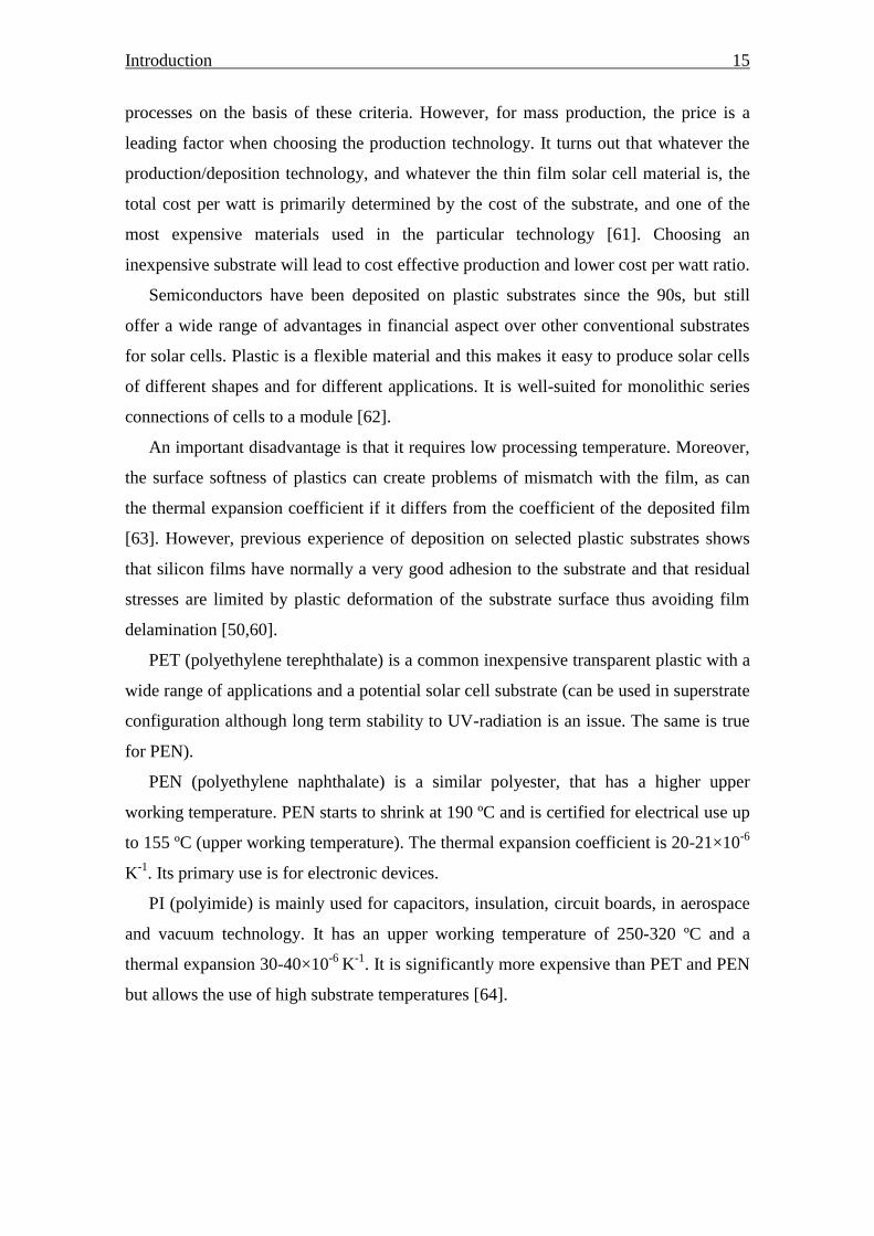
Reported efficiencies of thin film silicon solar cells on flexible substrates from
several research groups are included in table 1.1 for reference.
Table 1.1 Reported efficiencies at AM1.5 light condition of thin film silicon solar cells on plastic
substrates (from [65]).
SS: stainless steel; E/DT: tetracyclododecene co-polymer; LCP: liquid crystal polymer; PEN:
polyethylene naphtalate; PET: polyethylene terephtalate; Kapton: polyimide; *AM0 light condition; D:
direct deposition; T: transfer method; DT: direct deposition + tranfer.
1.2 Piezoresistive sensors
First discovered by Lord Kelvin in 1856, the piezoresistive effect is a widely used
sensor principle. Simply put, an electrical resistor may change its resistance when it
experiences a strain and deformation. This effect provides an easy and direct
energy/signal transduction mechanism between the mechanical and the electrical
domains. Today, it is used in the MEMS field for a wide variety of sensing applications,

Introduction 13
including accelerometers, pressure sensors [41], gyro rotation rate sensors [42], tactile
sensors [43], flow sensors, sensors for monitoring structural integrity of mechanical
elements [44], and chemical/biological sensors.
The piezoresistive property of crystalline silicon (c-Si) was first reported by C.
Smith [45]. Since then, many Si-based sensors use that property as their operation
principle [46-49]. In particular, doped silicon exhibits remarkable piezoresistive
response characteristics among all known piezoresistive materials [45]. By strict
definition, piezoresistors refer to resistors whose resistivity changes with applied strain.
Metal resistors change their resistance in response to strain mainly due to the shape
deformation mechanism. Such resistors are technically called strain gauges. The
resistivity of semiconductor silicon changes as a function of strain. Silicon is therefore a
true piezoresistor.
Piezoresistive sensors measure strain from the relative resistance change of a Si
transducer that is deformed to the strain to be measured. Piezoresistance in c-Si is
highly anisotropic and is described by a set of coefficients that are the elements of the
piezoresistive tensor, relating the change in electrical resistivity in a particular
crystallographic direction to the components of the applied stress tensor.
Polycrystalline metallic strain-gauge sensors are also common but they are much
less sensitive than their semiconductor counterparts [49]. This is because their operation
is mainly based on resistance variation due to stress-induced dimensional changes and
not on changes on the resistivity itself, as it is the case with Si (or Ge) sensors. In a
semiconductor, volume changes due to strain affect both carrier concentration and
carrier mobility, leading to resistance changes. But more important, in strained Si,
potentials modify the band structure near the edge of the conduction and valence bands,
leading to changes in carrier effective mass and/or occupancy of the density of states at
energies close to the Fermi level. This mechanisms dramatically enhance the
piezoresistive effect in semiconductors when compared to metals [45,49]. As the Fermi
level position approaches the conduction or valence band edges the effect is expected to
be enhanced and therefore piezoresistance is more important in doped than in intrinsic
Si. However, both the physical origin and the corresponding values of the piezoresistive
coefficients are very different in p- and n-type material [45-48].
The piezoresistive effect has also been found in thin polycrystalline silicon films [45,
50]. Due to the semi-crystalline nature of these films the reported effect is rather
isotropic and it broadly averages the resistance changes of the randomly oriented

14 Chapter 1
crystallites, thus retaining the signal of the largest c-Si piezoresistive coefficient.
Moreover, grain boundaries also play a role in piezoresistance of microcrystalline films
and their net effect is to attenuate resistivity changes occurring in the crystalline grains
[53]. Physical models considering the role of intra-grain and intergrain mechanisms in
the piezoresistive properties of 3C-SiC have been recently proposed [54].
The combination of standard large scale, low cost, semiconductor micro-fabrication
methods with miniaturization of high sensitivity Si-based sensors on plastic substrates
opens a richness of application possibilities [50].
Electromechanical and interferometric methods have the highest sensitivity to detect
applied stress, of the order of 0.05 Pa [55]. The former may replace the latter in process
control industries; it has been demonstrated that micron-sized polysilicon piezoresistive
sensors, integrated at low cost in small chips, can simultaneously measure temperature,
differential and absolute pressure [56]. Differential deformations of less than 100 nm
and pressures of less than a few tenths of Pa have been detected in this way.
Another demonstration at the University of Peking, consisted in using polysilicon
piezoresistive sensors, micro-fabricated into cantilever-arrays, to detect a few ppm of
concentration of ammonia (NH3) [57]. These chemical sensors have potential to low
cost, water contamination control.
Another development consisted in using as position sensors, poly-crystalline
diamond thin films, with a piezoresistive gauge factor of 28, for implantable cochlear
probes [58].
The application of miniaturized Si-like piezoresistive sensors in biomedical
instruments to measure pressure with values of the order of 105 dyne/cm2 (blood
pressure in artery and intraocular eye), is becoming increasingly important. Because
they operate at low frequency bandwidth, signal to 1/f noise should be maximized [59].
Recently, P. Alpuim et al. reported the piezoresistive response, under low-frequency
oscillations, of n-type µc-Si:H thin film microresistors fabricated by HWCVD at 150 ºC
on plastic substrates using standard lithographic techniques [60].
1.3 Plastic substrates
The substrate is a passive component in the device and is required to be
mechanically stable, matching thermal expansion coefficient with deposited layers and
to be inert during the device fabrication. Suitable substrates are selected for different
Introduction 15
processes on the basis of these criteria. However, for mass production, the price is a
leading factor when choosing the production technology. It turns out that whatever the
production/deposition technology, and whatever the thin film solar cell material is, the
total cost per watt is primarily determined by the cost of the substrate, and one of the
most expensive materials used in the particular technology [61]. Choosing an
inexpensive substrate will lead to cost effective production and lower cost per watt ratio.
Semiconductors have been deposited on plastic substrates since the 90s, but still
offer a wide range of advantages in financial aspect over other conventional substrates
for solar cells. Plastic is a flexible material and this makes it easy to produce solar cells
of different shapes and for different applications. It is well-suited for monolithic series
connections of cells to a module [62].
An important disadvantage is that it requires low processing temperature. Moreover,
the surface softness of plastics can create problems of mismatch with the film, as can
the thermal expansion coefficient if it differs from the coefficient of the deposited film
[63]. However, previous experience of deposition on selected plastic substrates shows
that silicon films have normally a very good adhesion to the substrate and that residual
stresses are limited by plastic deformation of the substrate surface thus avoiding film
delamination [50,60].
PET (polyethylene terephthalate) is a common inexpensive transparent plastic with a
wide range of applications and a potential solar cell substrate (can be used in superstrate
configuration although long term stability to UV-radiation is an issue. The same is true
for PEN).
PEN (polyethylene naphthalate) is a similar polyester, that has a higher upper
working temperature. PEN starts to shrink at 190 ºC and is certified for electrical use up
to 155 ºC (upper working temperature). The thermal expansion coefficient is 20-21×10-6
K-1
. Its primary use is for electronic devices.
PI (polyimide) is mainly used for capacitors, insulation, circuit boards, in aerospace
and vacuum technology. It has an upper working temperature of 250-320 ºC and a
thermal expansion 30-40×10-6
K-1
. It is significantly more expensive than PET and PEN
but allows the use of high substrate temperatures [64].
16 Chapter 1
1.4 Organization of the thesis
The work in this thesis can be divided in three parts: (1) the development of high-
rate deposited intrinsic and doped layers on plastics (2) the development of flexible thin
film silicon solar cells on transparent and opaque plastic substrates and (3) the
fabrication of strain gauge sensors based on the piezo-resistive properties of the doped
layers deposited on plastics.
The thesis is organized in seven chapters. An introduction to the topic in which this
thesis is inserted and a discussion of the state-of-the-art are done in the first chapter. The
last chapter summarizes the conclusions obtained in this work.
Chapter 2 describes the deposition and characterization techniques used during this
work. We used Plasma Enhanced Chemical Vapor Deposition (rf and VHF) and Hot
Wire CVD for the deposition of silicon thin films. In this part are also discussed the
main mechanisms of films growth and the role of hydrogen in these processes. The
description of the characterization techniques covers the structural and optoelectronic
techniques used for the thin films analysis and the techniques used for solar cell
characterization. The results and discussions concerning the studies realized in this
thesis are organized in the remaining chapters as follows:
High-rate deposited intrinsic and doped layers on plastics
Chapter 3 presents and discusses the results about the structural and optoelectronic
properties of a-Si:H and µc-Si:H intrinsic and doped layers deposited by rf-PECVD on
plastic (PEN) at 150 ºC. The study is focused in the optimization of the layers by
studying the influence of deposition pressure and power coupled to the plasma on the
deposition rate and film electronic quality.
Flexible thin film silicon solar cells
Chapter 4 deals with the development of amorphous silicon solar cells at a substrate
temperature of 150 ºC on PEN/TCO, in the superstrate p-i-n configuration, and on PI
foils at a substrate temperature of 200 ºC, in the substrate n-i-p configuration. The
results about room temperature deposited doped ZnO films on plastic substrates are also
shown in this chapter. Their optical, electronic and structural properties were correlated
and optimized. Also, light trapping effects were explored by laser texturing plastic
substrates. Their haze, total transmittance and reflectance were compared with those of
untextured substrates.
Introduction 17
Chapter 5 shows the development of microcrystalline thin film silicon solar cells at a
substrate temperature of 200 ºC, in the substrate n-i-p configuration on PI foils. It also
shows the achievement of textured back reflectors for the solar cells on PI, by wet
etching of a TCO layer followed by a highly reflective Ag/ZnO double layer coating.
Solar cells on flat and textured glass and PI are compared and the results discussed.
These results were obtained at Forschungszentrum Jülich (IEK-5).
Flexible strain gauge sensors
Chapter 6 describes the manufacture and characterization of a thin skin-like piezo-
resistor strain-sensing membrane and the miniaturization of piezoresistive sensor arrays
based on n-type hydrogenated microcrystalline silicon thin films (µc-Si:H) deposited on
flexible polyimide substrates (PI). The µc-Si:H thin films were prepared by hot-wire
chemical vapor deposition, and had a piezoresistive gauge factor of -32.2.
The main results showed in the chapters of this thesis were presented to the scientific
community in international conferences and published in international scientific
journals widely disseminated in their research area. The publications related to this
thesis were:
Chapter 3:
E. Marins, V. Guduru, M. Ribeiro, F. Cerqueira, A. Bouattour and P. Alpuim.
High-rate deposition of nano-crystalline silicon thin films on plastics. Phys.
Status Solidi C V. 8, No. 3, p. 846–849, 2011.
Chapter 4:
P. Alpuim, A. Samantilleke, E. Marins, F. Oliveira, M.F. Cerqueira, L.
Rebouta, S. Stefanov, S. Chiussi, C. Serra, J.E. Bourée. Amorphous silicon thin-
film solar cells deposited on flexible substrates using different zinc oxide layers.
Phys. Status Solidi C V. 7, No. 3–4, p. 1061–1064, 2010.
Chapter 5:
E. Marins, M. Warzecha, S. Michard, J. Hotovy, W. Boettler, P. Alpuim and F.
Finger. Flexible n-i-p thin film silicon solar cells on polyimide foils with
textured ZnO:Ga back reflector. Thin Solid Films, V. 571, p. 9-12, 2014.
Chapter 6:
P. Alpuim, E. Marins, P.F. Rocha, I.G. Trindade, M.A. Carvalho, S. Lanceros-
Mendez. Ultra-Sensitive Shape Sensor Test Structures Based on Piezo-Resistive
Doped Nanocrystalline Silicon. Vacuum, V. 83, p. 1279–1282, 2009.
P. Alpuim, V. Correia, E. Marins, J.G. Rocha, I.G. Trindade and S. Lanceros-
Mendez. Piezoresistive silicon thin film sensor array for biomedical applications.
Thin Solid Films, V. 519, p. 4574–4577, 2011.
18 Chapter 1
References
[1] A. Shah, ed., Thin-film Silicon Solar Cells, First edition, EPFL Press, 2010.
[2] Photon International, March 2009, p. 170.
[3] M.A. Green, Physica E: Low-dimensional Systems and Nanostructures, 14 (2002) p. 65.
[4] A. Müller, B. Ghosh, R. Sonnenschein, P. Woditsch, Materials Science and
Engineering: B, 134 (2006) p. 257.
[5] V. Fthenakis, S. Gualtero, R. van der Meulen, H.C. Kim, Materials Research Society
Symposium Proceedings, 1041 (2008) p. 25.
[6] V. Fthenakis, H.C. Kim, E. Alsema, Environmental Science and Technology, 42 (2008)
p. 2168.
[7] C. Wadia, A.P. Alivisatos, D.M. Kammen, Environmental Science and Technology, 43
(2009) p. 2072.
[8] D.E. Carlson and C.R. Wronski, Appl. Phys. Lett,. 28 (1976) p. 671.
[9] J. Meier, R. Fluckiger, H. Keppner, A. Shah, Appl. Phys. Lett., 65 (1994) p. 860.
[10] J. Meier, P. Torres, R. Platz, S. Dubail, U. Kroll, J.A.A. Selvan, N.P. Vaucher, Ch. Hof,
D. Fischer, H. Keppner, A. Shah, K.-D. Ufert, P. Giannoules, J. Koehler, Mater. Res.
Soc. Symp. Proc., 420 (1996) p. 3.
[11] T. Baba, et al., In Proceedings of the 13th European Photovoltaic Solar Energy
Conference, Nice, France (1995) p.1708.
[12] A. Shah, H. Schade, M. Vanecek, J. Meier, E. Vallat-Sauvain, N.Wyrsch, U. Kroll, C.
Droz and J. Bailat, In Proceedings of the Technical Digest of the 14th International
Photovoltaic Science and Engineering Conference, Bangkok, Thailand (2004) p. 39.
[13] R.A. Street, J. Zesch, M.J. Thompson, Appl. Phys. Lett., 43 (1983) p. 672.
[14] Guy Beaucarne, Advances in OptoElectronics, (2007), Article ID 36970.
[15] D.L. Staebler, C.R. Wronski, Appl. Phys. Lett., 31 (1977) p. 292.
[16] J. Meier, S. Dubail, R. Flückiger, D. Fischer, H. Keppner, and A. Shah, In Proceedings
of the 1st IEEE World Conference on Photovoltaic Energy Conversion, Hawaii, USA, 1
(1994), p. 409.
[17] H. Liu, S. Jung, Y. Fujimura, Y. Toyoshima, H. Shirai, Jpn. J. Appl. Phys. 40 (2001) p.
L215.
[18] G. Cicala, P. Capezzuto, G. Bruno, J. Vac. Sci. Technol. A, 19 (2001) p. 515.
[19] P. Alpuim, V. Chu, J.P. Conde, J. Appl. Phys. 86 (1999) p. 3812.
[20] S.A. Filonovich, P. Alpuim, L. Rebouta, J.-E. Bourée, Y. M. Soro, Journal of Non-
Crystalline Solids, 354 (2008) p. 2376.
Introduction 19
[21] P. Alpuim, G.M. Junior, S.A. Filonovich, P. Roca i Cabarrocas, J.-E. Bouree, E.V.
Johnson, Y.M. Soro, 23rd
European Photovoltaic Solar Energy Conference and
Exhibition (23rd EU PVSEC), Valencia, Spain (2008) p. 2455.
[22] Y. Wang, X. Geng, H. Stiebig and F. Finger, Thin Solid Films, 516 (2008) p. 733.
[23] H. Sannomiya, K. Nomoto, A. Chida, Y. Nakata, Y. Yamamoto, 1st IEEE World
Conference on Photovoltaic Energy Conversion, Hawaii, USA (1994) p. 405.
[24] M. Topic, F. Smole, J. Furlan, In Proceeding of 25th PVSC, Washington DC, USA
(1996) p. 1109.
[25] X. Deng, S.J. Jones, T. Liu, M. Izu, S.R. Ovshinsky, In Proceeding of 26th PVSC,
Anaheim, CA, USA (1997) p. 591.
[26] Y. Hattori, D. Kruangam, K. Katoh, Y. Nitta, H. Okomoto, Y. Hamakawa, In Tech.
Dig. Int. PVSEC-3, Tokyo, Japan (1987) p. 171.
[27] Z. Hu, Xianbo Liao, Hongwei Diao, Yi Cai, Shibin Zhang, Elvira Fortunato, Rodrigo
Martins, Journal of Non-Crystalline Solids, 352 (2006) p. 1900.
[28] J.K. Rath, Solar Energy Materials & Solar Cells, 76 (2003) p. 431.
[29] Y. Mai, S. Klein, R. Carius, J. Wolff, A. Lambertz, and F. Finger, J. Appl. Phys. 97
(2005) p. 114913.
[30] J.K. Rath, Y. Liu, A. Borreman, E.A.G. Hamers, R. Schlatmann, G.J. Jongerden, R.E.I.
Schropp, Journal of Non-Crystalline Solids, 354 (2008) p. 2381.
[31] E. Middelman, et. al., In Proceedings of the 2nd
World Conference and Exhibition on
Photovoltaic Solar Energy Conversion (WCPEC-2), Vienna, Austria (1998) p. 816.
[32] T. Söderström, F.-J. Haug, V. Terrazzoni-Daudrix, and C. Ballif, J. Appl. Phys. 103
(2008) p. 114509.
[33] C. Ballif, J. Bailat, D. Dominé, et al., In Proceedings of the 21st European Photovoltaic
Solar Energy Conference, Dresden, Germany (2006) p. 1552.
[34] K. Yamamoto, A. Nakajima, M. Yoshimi, et al., In Technical Digest of the 15th
International Photovoltaic Science and Engineering Conference (PVSEC ’05),
Shanghai, China, 1 (2005) p. 529.
[35] F.-J. Haug, T. Söderström, M. Python, V. Terrazzoni-Daudrix, X. Niquille, C. Ballif,
Solar Energy Materials and Solar Cells, 93 (2009) p. 884.
[36] T. Minemoto, M. Toda, S. Nagae, et al., Solar Energy Materials and Solar Cells, 91, no.
2-3 (2007) p. 120.
[37] A. V. Shah, H. Schade, M. Vanecek, Progress in Photovoltaics: Research and
Applications, 12, no. 2-3, (2004) p. 113.
[38] M. van Cleef, P. Lippens, and P. Call, In Proceedings of the 17th European Photovoltaic
Solar Energy Conference, Munich, Germany (2001).
[39] M.K. van Veen, R.E. Schropp, Thin Solid Films, 403–404 (2002) p. 135.
20 Chapter 1
[40] J. Yang, Baojie Yan, Subhendu Guha, Thin Solid Films, 487 (2005) p. 162.
[41] S. Sugiyama, M.Takigawa, and I. Igarashi, Sensors and Actuators A, 4 (1983) p. 113.
[42] F. Gretillat, M.-A. Gretillat, and N.F. de Rooij, Journal of Microelectromechanical
Systems, 8 (1999) p. 243.
[43] B.J. Kane, M.R. Cutkosky and T.A.Kovacs, Journal of Microelectromechanical
Systems, 9 (2000) p. 425.
[44] C. Hautamaki, et al., Journal of Microelectromechanical Systems, 8 (1999) p. 272.
[45] C.S. Smith, Physics Review, 94 (1954) p. 42.
[46] W.G. Pfann and R. N. Thurston, J. Appl. Phys. 32 (1961) p. 2008.
[47] O.N. Tufte, P.W. Chapman and D. Long, J. Appl. Phys. 33 (1962) p. 3322.
[48] I. Goroff, L. Kleinman, Phys. Rev. 132 (1961) p. 1080.
[49] M. Elwenspoek, R. Wiegerink, Mechanical Microsensors, Springer, New York (2001)
p.87.
[50] P. Alpuim, V. Chu, J.P. Conde, IEEE Sensors J. 2 (2002) p. 336.
[51] S. Nishida, M. Konagai, K. Takahashi, Jpn. J. Appl. Phys. 25 (1986) p. 17.
[52] P. Alpuim, S. Lanceros-Mendez, V. Sencadas, M. Andrade, S.A. Filonovich,
communication to the E-MRS Spring Meeting (E-MRS - IUMRS - ICEM 06), May 29 -
June 2, Nice, France (2006).
[53] L. Fang, W. L. Wang, P. D. Ding, K. J. Liao and J. Wang, J. Appl. Phys. 86 (1999) p.
5185.
[54] M. Eickhoff, M. Stutzmann, J. Appl. Phys. 96 (2004) p. 2878.
[55] Milton Ohring, "The materials Science of Thin Films", Chapter 9.4, Academic Press
Inc. (1992) p. 421.
[56] R. Pryputniewicz et al., In Proceedings of Internat. Symp. On Microscale Systems,
Orlando FL, USA (2000) p. 76.
[57] Yu Xiao-Mei et al., Chin. Phys. Lett., 20 (2003) p. 1637.
[58] Y. Tang, M. Aslam, J. Wang and K. Wise, "Fabrication and test of Poly-Crystalline
Diamond Piezoresistive Sensors for Cochlear Implant Probe", report ECE department,
Michigan State University.
[59] B. Bae, B. Flachsbart, K. Park and M. Shannon, J. Micromech. Microeng. 14 (2004) p.
1597.
[60] P. Alpuim, V. Correia, E. Marins, J.G. Rocha, I.G. Trindade and S. Lanceros-Mendez,
Thin Solid Films, 519 (2011) p. 4574.
[61] K. L. Chopra, P. D. Paulson, and V. Dutta, Thin-Film Solar Cells: An Overview,
Progress in Photovoltaics: Research and Applications, 12 (2004) p. 69.
[62] M. Kimming, Master's thesis, Lund University (2005).

Introduction 21
[63] F. Sarto, M. Alvisi, E. Melissano, A. Rizzo, S. Scaglione, and L. Vasanelli, Thin Solid
Films, 346(1) (1999) p. 196.
[64] Q. Wang, E. Iwaniczko, J. Yang, K. Lord, S. Guha, K. Wang, and D. Han, In
Proceedings of 29th IEEE PV Specialists Conference, New Orleans, Louisiana, USA
(2002) p. 1222.
[65] J.K. Rath, M. Brinza, Y. Liu, A. Borreman and R.E.I.Schropp, Solar Energy Materials
& Solar Cells, 94 (2010) p. 1534.

22 Chapter 2
Chapter 2
2 Experimental Techniques
The techniques that have been used for the deposition and characterization of the a-
Si:H and μc-Si:H layers and solar cells, are described in this chapter.
2.1 Plasma Enhanced Chemical Vapor Deposition
In general, thin films may be fabricated either by physical vapor deposition (e.g.,
evaporation or sputtering) of the bulk material, or by chemical vapor deposition
from the decomposition of suitable gases that contain the desired film material.
Historically both evaporation and sputtering of elemental silicon were used to obtain
thin films of amorphous silicon. However, these films contained high defect
concentration, mostly caused by poorly coordinated Si atoms, i.e. by so-called
“dangling-bonds”. Due to these high defect concentrations, the gap states
density between the valence and conduction bands far exceeds the dopant densities that
can be typically achieved. Therefore, this material is not suitable for use in an
electronic semiconductor device, which inherently requires the presence of n- and/or p-
type regions.
The high density of defect states can be somewhat reduced through post-
hydrogenation by heating the films in a hydrogen atmosphere, or, in the case of
sputtering, by adding hydrogen to the sputtering gas. However, these methods of
preparation have not proved successful in the further development of suitable
materials for electronic applications. Since it was recognized that silicon films
deposited at low temperatures require the presence of hydrogen to "saturate" or
"passivate" the dangling bonds, Chemical Vapor Deposition (CVD) methods have been

24 Chapter 2
chosen with a source containing both silicon and hydrogen, which is then decomposed
by supplying thermal or electrical energy to generally form hydrogenated amorphous
silicon (a-Si:H) films. Thus, in 1969, the decomposition of silane (SiH4) in a glow
discharge yielded hydrogenated amorphous silicon films with good photoconductivity
[1], indicating a defect concentration well below the generated photocarrier
concentration. Adding a dopant gas to the silane, glow discharge deposition has opened
the way for the effective doping of a-Si:H thin films [2], and hence for the possibility of
creating electronic thin-film devices.
Since then the development of Si-based thin films for PV applications has largely
remained based on the decomposition of silane as the Si precursor source material.
Other gases have also been used, like the chlorinated silane source gases such as
SiH2Cl2, SiHCl3, and SiCl4, in order to reduced the growth temperature. Several forms
of energy supply for the decomposition of the reactant gases have been developed,
namely:
• electrical energy, supplied in a glow discharge (plasma) for plasma-enhanced
chemical vapor deposition (PECVD):
• thermal energy by heating a filament, for thermo-catalytic chemical vapor
deposition (Cat-CVD), more commonly called Hot-Wire CVD (HWCVD).
• Photo-CVD or Laser-CVD (radiant energy)
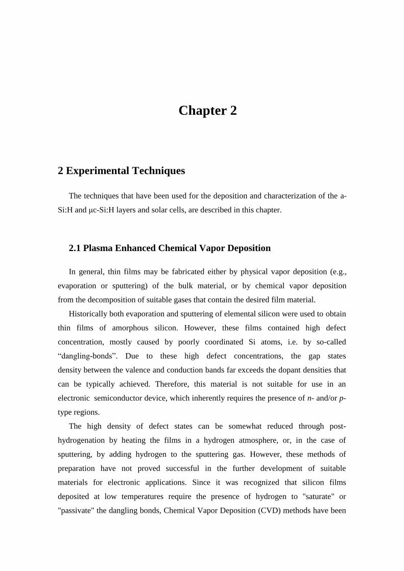
PECVD is conducted in a plasma reactor that, in the parallel plate capacitive
geometry, usually consists of
• a vacuum chamber, equipped with an inlet for the reaction gases, and pumps to
remove unreacted and reacted gases;
• a pair of parallel electrodes, one grounded and acting as the support for the
substrate to be coated, and the other connected to an electrical power supply, and
possibly also acting as a shower head to uniformly distribute the reaction gases;
• a gas handling system;
• substrate heating.
This arrangement, schematically shown in Figure 2.1, facilitates the sequential
deposition of the entire semiconductor structure, either in a single-junction or a multi-
junction (tandem or triple cell) configuration, as pin or pin/pin etc. To this end, not only
silane is used (as is basically sufficient for the intrinsic i-layer), but also doping gases
containing boron and phosphorus, such as diborane (B2H6) or trimethylboron [B(CH3)3],
and phosphine (PH3), for depositing p- and n-layers, respectively. Additionally, the
Experimental Techniques 25
energy gaps of the semiconductor film may be varied by adding gases containing other
group-IV elements, specifically
• methane (CH4) in order to alloy with carbon and, thus, to increase the energy
gap of the p-layer to create a window layer;
• germane (GeH4) in order to alloy with germanium and, thus, to decrease the
energy gap of the i-layer for enhanced red-response, particularly for multi-
junction cell structures.
PECVD is an extremely complex process involving a multitude of interactions
between the plasma, chemical reactions of the gases and their reaction products, as well
as interactions with the surrounding surfaces, ultimately including the substrate to be
coated.
Fig. 2.1: Schematic of PECVD reactor (from [3])
The application of a sufficiently high RF voltage (typically at the industrial
frequency of l3.56 MHz) to a capacitive configuration of parallel electrodes in a
container filled with gas at low pressure leads to the generation of a low-pressure
plasma, also designated as “cold plasma” or “glow discharge (GD)”. The plasma
reactions occur while the gas and the parts exposed to the plasma remain at relatively
low temperatures. The plasma is ignited by the generation of electrons and ions, due to
the ionization of gas molecules (initiated by ever-present cosmic rays), followed by
subsequent secondary electron emission from the electrodes, and further ionizations
with charge carrier multiplication. The ignition of the plasma may sometimes require
high voltage pulses supplied from a Tesla coil via a high-voltage feedthrough.
The plasma contains electrons, positive and negative ions, as well as neutral atoms,
molecules, free radicals, and metastable species. Basically, the described formation of
electrons and ions leads to various interactions with the gases, and gives rise to
chemical reactions and the formation of radicals and other reactive molecular fragments.

26 Chapter 2
Both concentration gradients and electrical fields support a mass transport by diffusion
and drift, respectively. Thereby interactions of various species including chemical
reactions with the substrate surface are initiated, and specific temperature-dependent
sticking coefficients and reaction actvation energies determine the composition and
structure of the film that is deposited.
Based on the use of the source gases silane (SiH4, also called, more specifically,
“monosilane”) and hydrogen (H2), the main chemical reactions may be grouped into
three categories [3]:
• electron impact dissociation, with the reactions
SiH4 + ē SiH2 + 2 H + ē
SiH4 + ē SiH3 + H + ē
H2 + ē 2 H + ē
• reactions with radicals
SiH4 + Ḣ ṠiH3 + H2
SiH3 + Ḣ ṠiH2 + H2
SiH4 + SiH2 Si2H6
• surface reactions that occur on the substrate, as well as on plasma-exposed
surfaces in the reactor; these reactions refer to the deposition of silicon radicals,
to etching by atomic hydrogen, and to hydrogen recombination at the surface:
SiH2 Sisurf. + H2
SiH3 2 Sisurf. + 3 H2
2 H H2
4 H + Sisurf. SiH4
Sisurf. refers to an a-Si:H or a µc-Si.H layer surface. One should note that the amount
of hydrogen needed to saturate dangling bonds is typically less than 1% of the total
hydrogen content in the film. The amount of hydrogen being incorporated into the
deposited silicon film is typically in the range 10-15 atom% or more, if deposition
occurs at low substrate temperature. However, the actual hydrogen content in the
deposited film (Sisurf.) is not apparent in the chemical reactions given above. For the
surface reactions, the availability of SiH2 and atomic hydrogen mainly determines the
balance between film growth and etching. This balance governs the degree of
Experimental Techniques 27
crystallinity from amorphous to microcrystalline silicon.
These reactions, in addition to those between higher silanes SinHm not shown here,
take place with different rate constants that are pressure- and temperature-dependent.
Other PECVD processes use Very High Frequency (VHF) plasma excitation in the
range of 30-300 MHz and will be discussed later in section 2.1.2.
PECVD can also be done using remote plasma, often inductively coupled to the
electrodes which are designed like antennas or coils. In remote plasmas the reactor
region where the plasma is generated is different from the region where the substrate is
placed. This allows to inject different reactant gases in different regions of the reactor,
namely in the plasma cavity and in the deposition chamber region. Both regions are in
vaccum and are connected by an aperture. The advantage of such geometries is to avoid
contact between the film growing surface and the plasma thus avoiding surface damage
by ion bombardment.
2.1.1 Electrical plasma properties
The voltage required for plasma ignition depends on the gas pressure p and on the
electrode spacing d; it is determined by the Paschen curve; a curve which features a
minimum for the ignition voltage at a specific value of p × d [3].
An electric potential distribution between the electrodes is established; it depends on
the applied RF voltage URF, and on the areas of the electrodes (inc1uding grounded
shields or reactor parts exposed to the plasma). The potential distribution is given by the
energy distributions of the electrons and ions that are exposed to the electric fields
between the electrodes. These electric fields are set up in the vicinity of the electrodes.
The basic mechanism is as follows: electrons have much higher thermal velocities than
ions, and can, thus, reach the electrodes faster, leaving the ions behind. To preserve
overall charge neutrality and to render net currents zero, electric fields develop near the
electrodes, retarding electrons and accelerating ions. These fields in front of the
electrodes extend over relatively small distances (typically in the order of a fraction of a
millimeter), which are determined by the resulting space charge densities. These regions
in front of the electrodes are positively charged, are composed mostly of ions, and
represent the so-called “sheaths”, as illustrated in figure 2.2. The sheaths are responsible
for ion bombardment. At higher plasma excitation frequencies the sheaths become

28 Chapter 2
thinner; this also means lower energies for the ion bombardment.
Fig. 2.2: Positive space charge region (so-called sheath), and field-free plasma volume (also called
plasma bulk) (From [3]).
As a result of the generated fields, the following time-averaged potentials are
assumed (see fig. 2.3):
• the so-called self-bias Vsb for the RF-powered electrode;
• zero potential for the grounded electrode; it is to the grounded electrode that one
normally fixes the substrate to be deposited. The substrate surface is separated
from the grounded electrode surface by the substrate thickness (i.e. usually by
the glass thickness), and takes on (in case of an electrically isolating substrate) a
certain relatively small potential, which is not specifically shown in figure 2.3;
• the plasma potential Vp; since, due to their thermal velocities, more electrons
than positive ions leave the plasma, the bulk of the plasma between the sheaths
assumes a positive plasma potential Vp;
• the potential differences across the sheaths (sheath voltages); these are Uc in
front of the RF-powered electrode, and UA in front of the grounded electrode,
respectively.
Fig. 2.3: Potentials and sheath voltages in a plasma reactor (from [3]).

Experimental Techniques 29
2.1.2 VHF plasma excitation
The frequency of 13.56 MHz (generally called “rf”, radio frequency) corresponds to
the standard frequency reserved by the International Electrotechnical Commission (IEC)
for Industrial High-Frequency Applications. It is therefore also the frequency that has
traditionally been most widely used. However, benefits in applying higher frequencies
extending into the range of 30-300 MHz (generally called “VHF”, very high frequency)
have been recognized for quite some time [4]. As a result, the use of higher excitation
frequencies has led to higher deposition rates, without sacrificing film quality. The ion
energies become lower with higher plasma frequencies, while at the same time higher
deposition rates are achieved.
All attempts to raise the deposition rate by increasing the plasma power are generally
limited by the onset of powder formation within the gas phase. At higher frequencies
the electric fields of the plasma discharge are smaller, and also the composition of the
radicals may be less conducive to gas-phase polymerization. In effect higher deposition
rates at VHF are clearly compatible with powder-free plasmas. However, to obtain
uniform deposition across large areas the VHF technology faces problems, and several
approaches aimed at combining the higher deposition rates, due to higher plasma
excitation frequencies, with acceptable deposition uniformities over large areas have
been attempted.
Depending on the ion energy, ion bombardment affects the quality of the growing
film in two ways:
• For ion energies larger than the threshold energy for defect generation
(approximately 15 eV), which typically applies to reactor operation at the
standard RF, ion bombardment creates damage by breaking bonds, and by
forming weak bonds and microvoids.
• At higher frequencies, ion energies remain lower, i.e. below the threshold energy
for defect generation. These lower ion energies give rise to an increased surface
mobility of the deposited species on the growing film, and thus provide for
rearrangements of deposited species and more orderly film growth.
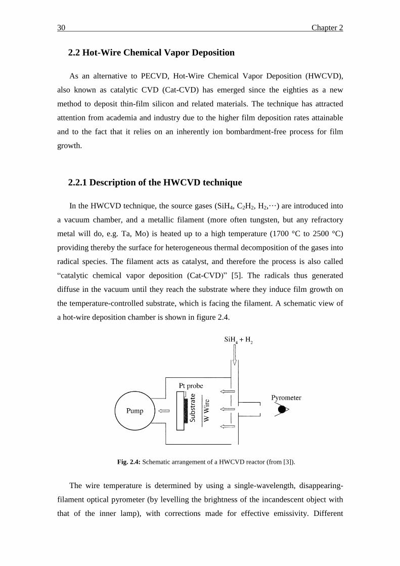
30 Chapter 2
2.2 Hot-Wire Chemical Vapor Deposition
As an alternative to PECVD, Hot-Wire Chemical Vapor Deposition (HWCVD),
also known as catalytic CVD (Cat-CVD) has emerged since the eighties as a new
method to deposit thin-film silicon and related materials. The technique has attracted
attention from academia and industry due to the higher film deposition rates attainable
and to the fact that it relies on an inherently ion bombardment-free process for film
growth.
2.2.1 Description of the HWCVD technique
In the HWCVD technique, the source gases (SiH4, C2H2, H2,···) are introduced into
a vacuum chamber, and a metallic filament (more often tungsten, but any refractory
metal will do, e.g. Ta, Mo) is heated up to a high temperature (1700 °C to 2500 °C)
providing thereby the surface for heterogeneous thermal decomposition of the gases into
radical species. The filament acts as catalyst, and therefore the process is also called
“catalytic chemical vapor deposition (Cat-CVD)” [5]. The radicals thus generated
diffuse in the vacuum until they reach the substrate where they induce film growth on
the temperature-controlled substrate, which is facing the filament. A schematic view of
a hot-wire deposition chamber is shown in figure 2.4.
Fig. 2.4: Schematic arrangement of a HWCVD reactor (from [3]).
The wire temperature is determined by using a single-wavelength, disappearing-
filament optical pyrometer (by levelling the brightness of the incandescent object with
that of the inner lamp), with corrections made for effective emissivity. Different
Experimental Techniques 31
spectroscopic techniques, such as threshold ionization mass spectrometry, single-photon
ionization or laser-induced fluorescence, can be attached to the reactor for probing the
radicals produced by hot-wire decomposition. The most important advantages of the
HWCVD process, as compared to the PECVD process are:
• Since the technique is thermal and catalytic in nature, and relies on a heated
metal filament to decompose the gas species, there are no ions (or are present in
a very small concentration) and electric fields present. Therefore, the substrate
and the growing film are not damaged by energetic ion bombardment. This is
important for depositing passivation or gas barrier films on organic devices. This
can also be important when depositing the first part of the i-layer in pin-type
solar cells, so as to avoid damage of the critical p/i-interface.
• Due to its high decomposition efficiency, the technique has the potential for high
deposition rates (up to 10 nm/s).
• Due to the low pressures that are used for gas phase decomposition (some
mTorr), a high flux of atomic hydrogen can be obtained; this can be useful for
material etching, for removing dangling bonds, and for enhancing the
abstraction of H atoms from the growing surface (leading, thereby, to a low H-
content in the films and to a premature aµc transition). At the same time, the
formation of SiH3, as growth pre-cursor, is favored due to H abstraction from
SiH4: H + SiH4 SiH3 + H2.
• Since no plasma is needed, the substrate is decoupled from the deposition
process, enabling substrates to be easily introduced and removed from the
deposition chamber without disturbing the deposition. Moreover, step coverage
(conformal film deposition) is excellent [7], and uniformity can easily be
optimized.
• It is a method that is easily scalable by expanding the spanned area of the
catalyst; this fact is particularly important for industrial implementation.
2.2.2 Filament materials
Over the last years, tungsten (W), which was previously the filament material most
frequently used, has gradually been replaced by tantalum (Ta), essentially when silane
flow is used. The replacement was motivated by the following consideration: to avoid

32 Chapter 2
filament aging, it is important to avoid the formation of silicides on the filament surface.
Now, the formation of Ta-silicide takes place at lower temperatures (only up to 1750 °C
under silane flow) when compared to the formation of W-silicide (up to l850°C) [8].
Apart from these two materials, ruthenium (Ru), rhenium (Re), iridium (Ir),
molybdenum (Mo), graphite (C) and a nickel-chromium alloy (NiCr) have also been
used occasionally as filament materials [3].
2.2.3 Types of materials deposited by HWCVD
The great majority of research activities on Hot-Wire deposition have so far been
devoted to gas phase and deposition chemistry of silicon-related materials:
hydrogenated amorphous silicon, microcrystalline silicon, polysilicon, epitaxial silicon,
silicon alloys with carbon, nitrogen and germanium. This research has also been done in
view of applying these materials, for instance, in solar cells and thin film transistors.
Since 2004, an increasing variety of thin-film materials have been obtained with the
HWCVD method, namely: silicon dioxide, aluminum oxide, aluminum nitride, Si-O-C,
Si-N-C alloys, diamond, carbon nanotubes, nanowalls or nanoparticles. Moreover,
transition metal oxide nanoparticles have been synthesized for applications like gas
sensors or electrochromic windows. A novel HWCVD variant, called “initiated CVD
(iCVD)”, appeared in 2006, and has spread rapidly [9]. It was demonstrated to be a
convenient single-step fabrication method to produce high-quality polymer thin films.
2.2.4 Mechanisms of the deposition process
Looking specifically at the deposition of a-Si:H layers, several researchers have
attempted to undertake a systematic study of the deposition process mechanisms for
HWCVD [10-13]. Optimum conditions for the deposition of amorphous silicon films
have been obtained [11] for a particular value of the gas phase parameter p × L, i.e. for
p × L ~ 20-75 mTorr.cm, where p is the silane chamber pressure in mTorr, and L is the
distance in cm between filament and substrate. They postulated that this optimum
results from the need to increase the pressure to a level where most Si atoms react with
SiH4 before reaching the substrate, while avoiding excessive gas phase reactions that
can lead, at still higher pressures, to the formation of large radicals, such as Si2H6 and
Experimental Techniques 33
Si3H8. SiH3 is considered to be a “good” film growth precursor [14] because it has high
surface mobility and has the longest lifetime among the various SiHn-type species; in
contrast to SiH2, it does not lead to the formation of large radicals.
The formation of radicals (especially of those radicals that are growth precursors) is
an essential point when studying the deposition of thin-film silicon layers. Radical
formation has been studied by various methods, as follows:
The nature and the flux of radicals desorbed from a hot filament depend on the
filament temperature and on the gas pressure in the reactor. In the case of a tungsten
filament heated at 1900 °C in a low pressure of silane, most of the authors agree that,
using different detection methods, one does detect different radical species, namely Si,
H and SiH3. Using threshold ionization mass spectrometry, H and Si were found as
primary radicals with a small contribution of SiH3 [10, 15] for a large range of
temperatures (1450 to 2700 ºC) and for H2 pressures up to 0.1 Torr, whereas using
single-photon ionization with a vacuum ultraviolet laser, gas-phase species identified
were Si, SiH, and Si2H6 [12]. In the latter case H was not detected because the
ionization potential for H exceeded the photon energy of the laser. Moreover,
considering newly replaced (“virgin”) filaments, the small activation energy (8
kcal/mol) then observed for SiH3 formation suggested that the process was “catalyzed”
[13].
The absolute density of H-atoms in the gas phase has been determined by combining
a two-photon laser-induced fluorescence technique and a vacuum ultraviolet (Lyman α)
absorption technique [16]. At high temperatures of the tungsten wire (~1930 ºC), the
absolute density of H-atoms reached values that were as high as 1.0 × 10¹⁴
cm-3
. These
values are two orders of magnitude higher than those obtained by PECVD under
comparable conditions. The effective enthalpy for the H-atom formation from H2 on the
catalyst surface was determined to be 57.1 kcal/mol [16] and should be compared with
the effective bond dissociation energy of gas-phase H2 molecules, which is 109.5
kcal/mol. This result established clearly the catalytic nature of the hot-wire CVD
process.
As concerns the mechanism of H-atom formation by HWCVD, it was demonstrated
that this mechanism proceeded via dissociative adsorption at bare sites followed by
desorption at hydrogenated sites on the hot wire surface [17].
34 Chapter 2
2.2.5 Filament aging
It has been suggested [18] that the electronic properties of a-Si.H deposited by HW-
CVD are related to radical chemistries, and that the differences observed in thin-film
properties are linked to the differences between a “virgin” wire and an aged wire. For an
aged wire, the SiH3 signal exhibited an activation energy of 106 kcal/mol: a value that is
much higher than the 8 kcal/mol observed for a “virgin” wire. This suggests that the
aging of the wire leads to a drastic reduction of its catalytic activity [13]. Also SiH and
SiH2 are now more abundant than SiH3, in contrast with the results obtained when a
“virgin” filament is used [13].
To gain insight into the nature of the changes occurring at the wire surface, scanning
electron micrographs and Auger electron spectroscopy were used to characterize the
surface morphology of heat-treated and aged wires, and to measure the Si
concentrations at the surface and in the interior of the wire, respectively. A Si
concentration of 15 at.% was observed at the surface of an aged wire, corresponding to
a two-phase equilibrium between tungsten silicide (W5Si3) and tungsten, whereas
approximately 2 at.% Si concentration was measured in the interior of the wire, a value
that is comparable to the equilibrium solid solubility of Si in W [13].
Using a tantalum filament exposed to a silane pressure of 0.25 Torr [19], the
formation of a Ta5Si3 shell (as determined by X-ray diffraction) of 20 µm thickness was
observed. After 4 hours of annealing of the filament in vacuum at high temperature
(2100 ºC), the tantalum silicide was completely removed. This regeneration procedure
was shown to greatly enhance the lifetime of the Ta filaments.
Based on these results, a Ta filament was used in all HWCVD depositions in the
present work.
2.3 CVD deposition systems
2.3.1 The CVD deposition system at Universidade do Minho
Figure 2.5 shows a picture of the CVD deposition system used at Universidade do
Minho for the development of silicon thin films, piezoresistive sensors and solar cells.
The CVD deposition system consists of twin chambers in cilindric format, made of
stainless steel, with conflat flanges and metallic seals of copper gaskets, for rf-PECVD

Experimental Techniques 35
and HWCVD deposition. These two chambers are connected in series with a load lock
chamber. A manually controlled transfer arm is used for loading and unloading a single
sample holder each time.
The pumping systems are independent for the three chambers and consist of
turbomolecular pumps backed by rotary pumps. Gate valves isolate the chambers from
each other and from the pumps, when necessary. The chambers are pumped by turbo-
molecular pumps, assisted by rotary vane pumps. The base pressure in each chamber is
lower than 10-7
Torr. The pressure is measured by Penning and Pirani gauges, and
controlled by a manual needle valve.
The gas supply to the chambers is carried out in the cross-flow mode by stainless
steel gas lines and the flow is controlled by Mass Flow Controlers (MFC). The substrate
temperature is controlled by a Eurotherm unit connected to a thermocouple and a heater.
Fig. 2.5: The CVD deposition system at Universidade do Minho consists of two UHV chambers assisted
by a load lock chamber. The chamber in left is for HWCVD depositions, and the chamber in the rigth is
for rf-PECVD depositions.
In the rf-PECVD chamber (right side in fig 2.5), a conventional design with two
parallel capacitive electrodes is used for the radio-frequency (13.56 MHz) discharge.
The power is supplied through the lower electrode. The sample is attached to the upper
electrode, which is kept in earth pontential by a feedthrough connected outside the
36 Chapter 2
system. The power source is connected to a tune unit with a variable reactance, which is
ajustable in order to eliminate the power reflected by the circuit.
In the HWCVD chamber (left side in fig. 2.5), the substrate holder is placed 5 cm
above a single tantalum filament (Ø = 0.5 mm, 14 cm long) that is bent in S shape and
fixed at its ends by support bars and ceramic pieces. The filament is resistively heated
for deposition, using a DC power supply that pyrolytically decompose the reactant gases
at the filament surface.
2.3.2 The CVD deposition system at Forschungszentrum Jülich
Figure 2.6 shows a drawing of the cluster tool deposition system used to prepare
individual layers and solar cells at Forschungszentrum Jülich [42]. The deposition
system is a multi-chamber system, it consists in total of seven chambers, which are
connected to the transfer chamber (TC). The transport of the samples between the
chambers is carried out by a robotic arm located in the transfer chamber. The loading
chamber MC1 can simultaneously load six substrates of 10×10 cm2. The substrates are
driven individually without breaking the vacuum, from the loading chamber into the
transfer chamber and to the deposition chambers. The heater station (HS) which, in
contrast to the other chambers, is not separated from the transfer chamber by a gate
valve, is used to pre-heat the substrates before each deposition. Alternatively, the
substrates are pre-heated in an unused deposition chamber. Chamber MC2 is another
loading chamber, loaded with one single substrate. In the event of a possible expansion
of the deposition system, another cluster tool can be connected trough the chamber
MC2, which might be used as the transfer chamber between two cluster tool deposition
systems. The chambers PC1, PC2 and PC3 are identically structured PECVD process
chambers. Chamber PC1 is used to deposit doped layers. In chamber PC2 intrinsic
layers are deposited, chamber PC3 is adapted for the processing of silicon alloys.
Chamber PC4 is a HWCVD process chamber for the deposition of intrinsic
microcrystalline layers. PC5 is a sputtering chamber used for TCO deposition. With
exception of the HS chamber, all the process chambers have a multistage pumping
system, which consists of a turbo-molecular pump, roots pump and a rotary vane pump.
By this configuration, pressures are in the range of Ultra High Vacuum. The pressure is
Experimental Techniques 37
measured by Penning and Pirani gauges, which depending on the measurement range
will automatically switch between each other.
Fig. 2.6: Schematic of the cluster-tool deposition system used at Forschungszentrum Jülich
(adapted from [42]).
Figure 2.7 shows schematically the structure of a process chamber. The chambers
PC1, PC2 and PC3 have a parallel plate configuration. The power input is delivered by
a copper strip connected below the RF / VHF electrode. The substrate holder, made of
stainless steel, is located above the electrode and acts as a grounded electrode. A
shutter, located just below the substrate is opened only when the plasma burns stable
and homogeneously. The distance between the substrate and electrode can be varied
between 5 mm and 20 mm. The heater is mounted over the substrate, which is pressed
against the heater so that there is a sufficiently good thermal contact between heater and
substrate. The working temperatures are measured by two thermocouples. One of the
thermocouples is in the heater shed, the second is attached to the side of the heater.
The gas supply to the chambers is carried out either via showerhead mode or in the
cross-flow mode. Because of the generally better layers homogeneity, all the samples
prepared with the cluster tool system were processed in the showerhead mode.
38 Chapter 2
Fig. 2.7: Schematic of a process chamber in the cluster-tool deposition system (adapted from [42]).
For safety reasons, the process gases are stored outside the laboratory. Using
appropriate gas lines, the process gases are conducted to a gas distribution system
within the laboratory. The flow of any process gas can be set and regulated by a mass
flow controller. The process gases are combined into each chamber by the valves SV1
and SV2. A separate argon (Ar) gas line is available in order to flush the line and the
chamber after each process step. The flow can also be adjusted using a MFC.
2.4 Optical transmittance spectroscopy
The common parts of UV-VIS-NIR spectroscopy techniques are light sources, beam
splitter or diffraction gratings, sample holders and detectors. The intensity (I0) of the
incident light after passing through the sample is changed to a lower value (I) due to the
absorption within the sample and/or reflection at the interfaces. The transmission or
absorption spectrum of a specific sample (thin film on a substrate) contains information
about the optical parameters of the film when compared with a reference sample.
In this work, a dual beam UV-VIS-NIR spectrometer set-up is used to characterize
silicon thin films. Reference sample (substrate) and the studied sample (substrate with

Experimental Techniques 39
silicon film) are put into two different sample holders. The light beam of wavelength
ranging from 250-3200 nm is split in two beams that simultaneously passed through
each sample. The difference between the reference beam and the beam coming from the
sample containing the film is recorded in the form of a spectrum. Depending on the film
thickness, interference fringes appear in the recorded spectrum. The appropriate analysis
of this spectrum yields the optical parameters of the film material. A typical
transmission spectrum of a film on a glass substrate is shown in figure 2.8. Oscillations
in the transmission spectra are observed due to interference effects in the film [20].
The optical parameters of the film can be calculated using the Swanepoel method
[43] from the transmission spectra. Thickness (d), refractive index (n), and absorption
coefficient (α) of the film can be evaluated using this method. The basic equation for
interference fringes is:
(2.1)
where m is an integer for maxima and half integer for minima, n is refractive index, d is
the thickness of the film, and λ is wavelength. The transmission T for the normal
incidence resulted from the interference of the wave transmitted from three interfaces
can be written as [43]:
( )
( ) (2.2)
where
(2.3a)
( ) ( ) (2.3b)
( )( ) (2.3c)
( ) ( ) (2.3d)
⁄ (2.3e)
( ) (2.3f)
For maximum and minimum points of interferences ( ) , so TM and Tm
curves as the upper and lower bounding functions of transmittance can be found by
fitting the two below curves to these points as

40 Chapter 2
(2.4)
(2.5)
If Ts, shown by dotted line in figure 2.8, is the maximum value of the transmission of
substrate, then substrate refractive index s can be given by the following equation:
(
)
⁄
(2.6)
The upper bounding function TM passes through the maxima of the spectrum and Tm
through the minima as shown in figure 2.8.
From equations 2.4 and 2.5, we have
(2.7)
The right hand side of equation 2.7 is independent of the thickness of the film.
Substituting C and A from equation 2.3 into equation 2.7 leads to:
[ ( ) ⁄ ] ⁄
(2.8)
where
( ) ⁄ ( ) ⁄ (2.9)
If n1 and n2 are the refractive indices calculated from two consecutive maxima or
minima corresponding to two wavelengths of λ1 and λ2, then the film thickness can be
obtained from [43]:
( ) (2.10)
The thickness obtained from equation 2.10 is very sensitive to the uncertainty in the
value of the refractive index which is derived from equation 2.8.
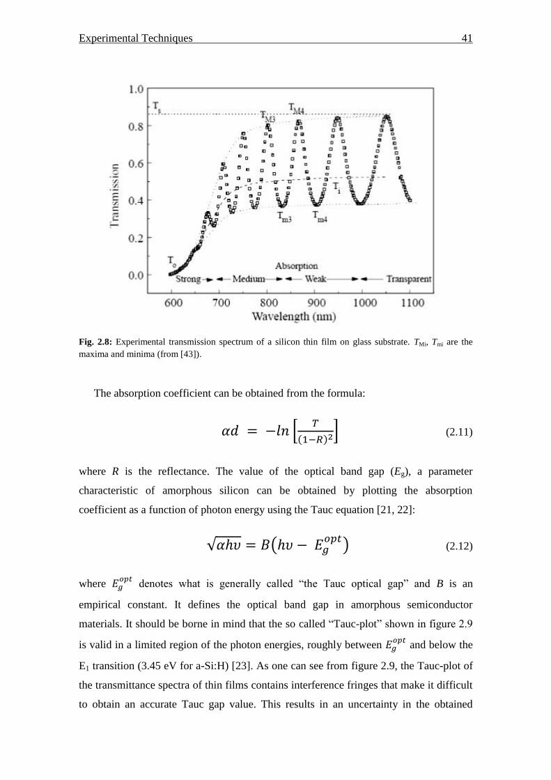
Experimental Techniques 41
Fig. 2.8: Experimental transmission spectrum of a silicon thin film on glass substrate. TMi, Tmi are the
maxima and minima (from [43]).
The absorption coefficient can be obtained from the formula:
[
( ) ] (2.11)
where R is the reflectance. The value of the optical band gap (Eg), a parameter
characteristic of amorphous silicon can be obtained by plotting the absorption
coefficient as a function of photon energy using the Tauc equation [21, 22]:
√ ( ) (2.12)
where
denotes what is generally called “the Tauc optical gap” and B is an
empirical constant. It defines the optical band gap in amorphous semiconductor
materials. It should be borne in mind that the so called “Tauc-plot” shown in figure 2.9
is valid in a limited region of the photon energies, roughly between
and below the
E1 transition (3.45 eV for a-Si:H) [23]. As one can see from figure 2.9, the Tauc-plot of
the transmittance spectra of thin films contains interference fringes that make it difficult
to obtain an accurate Tauc gap value. This results in an uncertainty in the obtained
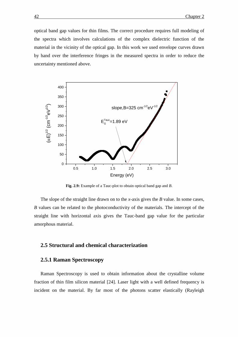
42 Chapter 2
optical band gap values for thin films. The correct procedure requires full modeling of
the spectra which involves calculations of the complex dielectric function of the
material in the vicinity of the optical gap. In this work we used envelope curves drawn
by hand over the interference fringes in the measured spectra in order to reduce the
uncertainty mentioned above.
0.5 1.0 1.5 2.0 2.5 3.0
0
50
100
150
200
250
300
350
400
(E
)1/2 (
cm
-1/2eV
1/2)
Energy (eV)
ETauc
G=1.89 eV
slope,B=325 cm-1/2
eV-1/2
Fig. 2.9: Example of a Tauc-plot to obtain optical band gap and B.
The slope of the straight line drawn on to the x-axis gives the B value. In some cases,
B values can be related to the photoconductivity of the materials. The intercept of the
straight line with horizontal axis gives the Tauc-band gap value for the particular
amorphous material.
2.5 Structural and chemical characterization
2.5.1 Raman Spectroscopy
Raman Spectroscopy is used to obtain information about the crystalline volume
fraction of thin film silicon material [24]. Laser light with a well defined frequency is
incident on the material. By far most of the photons scatter elastically (Rayleigh

Experimental Techniques 43
scattering) and a small part of the light scatters inelastically, which leads to a frequency
shift:
(2.13)
where is the energy of the scattered light, the energy of the incident light and
ΔE the energy shift that corresponds to the energy of a phonon that has been created
(Stokes scattering) of annihilated (anti-Stokes scattering).
The Raman shift spectrum reflects the phonon density of states. Within the detected
spectral range the transverse-optic (TO) mode of crystalline silicon is visible (520 cm−1
)
as well as the transverse-acoustic (TA), longitudinal-acoustic (LA; 330 cm−1
),
longitudinal-optic (LO; 445 cm−1
) and TO (480 cm−1
) modes of amorphous silicon.
Consisting of amorphous tissue and crystallites, µc-Si:H simultaneously shows a
crystalline peak and an amorphous peak in the Raman spectrum. In addition, a third
peak at around 500 cm−1
is often observed in the Raman spectra of µc-Si:H. This peak
was previously attributed to the stacking faults or hexagonal silicon [24, 25].
Fitting three Gaussian peaks the Raman spectra is an easy way to determine the
integrated intensities of crystalline and amorphous peaks. The integrated intensity ratio
of the Gaussian peaks, Xc, can be used as a semi-quantitative value for crystalline
volume fraction. This ratio is defined by the contributions of the different phases to the
TO mode:
(2.14)
where Ix denotes the integrated intensity of the contribution centered around x cm−1
. Ix
can be determined by means of a deconvolution of the Raman spectrum. Note that Xc is
only a semi-quantitative value, since the Raman cross sections are different for
crystalline and amorphous phase, and may depend on the excitation wavelength.
Furthermore, the absorption coeficient difference in the crystallites and in the
amorphous phase makes it more difficult to determine the real crystalline volume
fraction from Raman spectra. Still, Raman spectroscopy is a simple and useful method
to provide the structure information of the material, and thus is widely used.

44 Chapter 2
2.5.2 Fourier-Transform Infrared Spectroscopy (FTIR)
Various hydrogen related bonding configurations can be distinguished by Fourier-
Transform Infrared Spectroscopy (FTIR). Vibrational modes of non-symmetric (polar)
bonding configurations are reflected in the IR absorption spectra. The magnitude of the
absorption related to a certain mode is a measure for the number of associated bonds
present in the material. The proportionality constant is dependent on the oscillator
strength of the bond.
The thin films to be analyzed are deposited on a low resistivity c-Si wafer. The
measurements are performed with a spectrometer that is based on the principle of a
Michelson interferometer: the absorption spectrum is obtained by Fourier-transforming
the complex interference of two beams reflected at a fixed and a moving mirror,
respectively.
The absorption spectrum of the sample is corrected for the absorption of the
substrate that is measured as a reference. The recorded spectra are corrected for multiple
reflections in the substrate [26] and coherent reflections within the layer [27]. Si–H
bonds in the rocking mode at 640 cm-1
and the stretching mode at 2000 and 2100 cm-1
are analyzed. The hydrogen concentration is calculated from the rocking mode with the
proportionality constant 2.1×10¹⁹
cm-2
[28].
The microstructure factor R* is defined by the fraction of the Si–H stretching mode
bonds that are in the 2100 cm-1
mode. The 2100 cm-1
mode is attributed to Si–H2 bonds
or to Si–H bonds at grain surfaces or large internal voids. A high microstructure factor
is associated with an open material structure or to a high microcrystalline fraction.
2.6 Electrical Material Characterization
2.6.1 Dark Conductivity
In device-quality material, electronic transport in hydrogenated amorphous silicon
layers (and also in hydrogenated microcrystalline silicon) is very similar to transport in
classical, crystalline semiconductors.
It can therefore be well described by the so-called “standard transport model”. In this
model, both free electrons, i.e. electrons within the conduction band, as well as free
holes, i.e. holes within the valence band, travel by drift and/or by diffusion from one
Experimental Techniques 45
place to the other. On the other hand, localized electrons and holes (i.e. electrons and
holes trapped in their respective bandtails) do not contribute to the current. Thus, one
has for the respective electrical current densities [3]:
⁄ (2.15)
and
⁄ (2.16)
where q is the unit charge (charge of an electron), is the band mobility of electrons,
the band mobility of holes, the density of free electrons, the density of free
holes, E the eletric field prevailing at the point considered, the diffusion constant of
electrons, and the diffusion constant of holes.
The measurement of the dark conductivity of thin-film silicon layers is a basic and
important evaluation technique. For electrical measurements of the thin-film silicon
layers deposited on glass and on plastics, two coplanar metallic contacts are evaporated
parallel to each other. By applying a voltage V between the electrodes, and measuring
the resulting electrical current I in the dark, assuming the cross-section to simply be the
product of the thickness of the layer and of the side length of the rectangular contact
pad, the dark conductivity σd can be determined by the following equation:
(2.17)
where d is thickness, w is distance between the contacts, and l is contact length.
The value σd of the dark conductivity is generally found to vary exponentially with
the absolute temperature T (in Kelvin), i.e. we generally have a temperature dependence
of the form
( )
(2.18)
where σ0 is called the “conductivity prefactor”, k is the Boltzmann factor and is
denoted as “activation energy”.
By plotting the measured values versus (1/T), we obtain (more or less) a
straight line. In a first approximation, the extrapolation of this line to T = 0 gives us the
conductivity prefactor , and the slope of this line, also called the activation energy

46 Chapter 2
of the dark conductivity, gives us the value , or the value , i.e. the
position of the Fermi level , with respect to the nearest band edge.
2.6.2 Photoconductivity
The photoconductivity is an optoelectronic phenomenon consisting in an increased
electrical conductivity of a material when exposed to light. When the material absorbs
electromagnetic radiation, i.e. photons, there is an increase of the number of free charge
carriers (i.e. creation of electron-hole pairs) and, consequently, an increase in the
electrical conductivity of the material. In order to produce the excitation of extra charge
carriers, the light beam is focused on the sample surface and the photons should have
enough energy to cause the transition of electrons from valance band to conduction
band. This means that only the photons with energy higher than that of the optical gap
are absorbed in substantial quantity.
The photoconductivity is given by the following formula:
( ) (2.19)
Δn and Δp denote the concentrations of the photogenerated carriers which are
determined by the balance between the generation and recombination processes [29]. µe
and µh are mobilities of electrons and holes, respectively. The recombination of charge
carriers out of equilibrium is usually characterized by so called carrier lifetime. Strictly
speaking, the lifetime can be introduced only for minority carriers and under some
approximations [29]. If we assume that they are satisfied, the concentration of the
(photogenerated) minority carriers, at steady state conditions can be expressed as:
(2.20)
G is the generation rate of charge carriers per unit volume and τe is the electron lifetime
(we just assumed that electrons are the minority carriers). The generated free carriers
can recombine through recombination centers present in the material. The electronic
states related to defects, voids, dangling bonds and other deep centers, act as
recombination centers.

Experimental Techniques 47
In the case of a-Si:H and µc-Si:H films, it is known that the photoconductivity
mechanism is dominated by the electrons, due to their higher mobility. Then eq. (2.19)
can be written as:
( ) (2.21)
However, in reality, the dependence of the photoconductivity on the generation rate, G,
is not exactly linear as suggested by eq. (2.21). A more general power law has been
established [30],
(2.22)
where γ is a critical exponent of the power law. The values of γ for films of
hydrogenated amorphous and microcrystalline silicon are around 0.5 and 1, respectively
[29].
2.6.3 Constant Photocurrent Method (CPM)
The constant photocurrent method (CPM) allows to measure the absorption
coefficient for values of α·d « 1 down to α ~ 10-2
cm-1
. Here, one measures the
photoconductivity that has been induced by the absorption of the light at different
wavelengths: under certain circumstances, the value of the photoconductivity of a
semiconductor layer can be considered to be roughly proportional to the light absorbed
and to the density of charge carriers generated within the layer. In the CPM
measurement these circunstances are fulfilled because the generation rate is constant,
which fixes the pseudo-Fermi levels for both electrons and holes (By means of an
electronic regulation circuit, the photocurrent is kept constant and one correspondingly
modulates the amplitude of the monochromatic light for which one wishes to measure
the absorption. If the absorption coefficient is low at that specific wavelength, then a
high light intensity is required to obtain the fixed value of the photocurrent; if, on the
other hand, the absorption coefficient is high, then a low value of light intensity will be
sufficient. As one keeps the photocurrent (i.e. the density of charge carriers) constant, it
is not necessary to have an exact proportionality between the photoconductivity and the
density of charge carriers. As both electrons and holes contribute tho the
48 Chapter 2
photoconductivity, although in a slightly different manner, the CPM technique depends,
to a slight extent, on the position of the Fermi level EF. The basic CPM technique is
explained in more detail in [31].
A CPM spectrum can be divided into three parts: in the low energy range, the
absorption by defects dominates the evolution of α. Towards higher energy, α increases
exponentially with energy, this part is labeled Urbach tail. Here, mainly electron
excitation from valence band tail to the conduction band take place. The reciprocal
slope of the absorption coefficient in the Urbach tail region is known as Urbach energy
EU. The Urbach tail region is followed by higher band-to-band transitions with
corresponding energies.
As a measure of the integrated defect density Nd in a-Si:H, one can take the
absorption coefficient, αd, at the photon energy of 1.2 eV [32]: Nd = αd × Cd, where Cd is
a correction factor [33]. Good values for the defect density and EU in a-Si:H are around
1016
cm-3
and below 50 meV, respectively.
2.7 Solar Cell Characterization
2.7.1 Current-Voltage Measurements (IV)
The electrical output of solar cells is characterized by analyzing current density vs.
voltage (JV) measurements. The J-V measurements are normally performed in a solar
simulator under illumination calibrated to the AM1.5 spectrum [34] (integrated power is
100 mW/cm2). Ideal solar cells show the behavior of an equivalent circuit (fig. 2.10)
consisting of a photocurrent Jph source, a diode and a resistance Rp in parallel, connected
in series with a resistance Rs.
The current density is well described by [35]:
( ) [ ( ( )
) ]
(2.23)
where J0 is the dark saturation current, n is the diode quality factor (close to 1 for
diffusion-type cells and close to 2 for drift-type cells), k is the Boltzmann factor, and T
the absolute temperature.
Experimental Techniques 49
Fig. 2.10: Equivalent circuit of a solar cell with a diode, photocurrent source (Jph), parallel (Rp) and series
resistance (Rs).
J0 and n are derived from the dark J-V measurements (Jph = 0). From the J-V
characteristic under illumination, one can determine several parameters (see figure
2.11):
• The efficiency η is defined as the ratio of the maximum power generated by the
device (given by Pmax = Jmax × Vmax) and the incident radiation power. The efficiency
under AM1.5 illumination is the ultimate parameter characterizing each solar cell.
• The fill factor FF defined as
ocsc VJ
JVFF
maxmax
(2.24)
gives a description of the "rectangularness" of the light JV characteristic and is an
integral measure of the collection efficiency at the maximum power point.
• The short-circuit current density Jsc is the maximum current density generated by
the device.
• The open-circuit voltage Voc (voltage at J = 0 mA/cm2), is the maximum voltage
generated by the solar cell under illumination. In first approximation, the voltage
can be calculated from equation 2.23, using the assumptions of a constant
photocurrent and Jph = Jsc . Hence it follows (the parallel resistance is neglected):
1ln
0J
J
e
nkTV SC
OC (2.25)
Jph
50 Chapter 2
It is clear from eq.(2.25) that in order to achieve a high open-circuit voltage it is
necessary to have a low dark saturation current. The slope of the J-V curve at Jsc is
associated with the parallel resistance Rp and the slope at Voc with the series resistance
Rs. In order to achieve a high fill factor and Voc, the series resistance should be as small
and the parallel resistance as high as possible.
Fig. 2.11: Scheme of a light JV characteristic with important JV parameters (See text).
2.7.2 External Quantum Efficiency (EQE)
The External Quantum Efficiency (EQE) of solar cells is measured for light in the
wavelength range 300–1100 nm by measuring the current that is generated by a
monochromatic AC probe beam. The EQE is given by the number of collected electrons
per incident photon:
( ) ( ) ⁄
(2.26)
where e is the electron charge, Jph the generated current density, and ϕ the photon flux
incident on the sample. The total generated current density is given by the integral of the
convolution of the EQE with the AM1.5 photon flux spectrum [35].
∫ ( ) ( ) (2.27)
Experimental Techniques 51
2.8 Piezoresistance
The application of pressure to the crystal structure of a semiconductor material
temporarily alters its symmetry, and consequently modifies the conduction mechanism
which is highly sensitive to these variations. The observed macroscopic effect is a
resistivity variation [36]. This variation can be positive or negative; i.e., the pressure
may cause either an increase or a decrease of resistivity, according to the material and
the crystallographic direction along which it is applied.
The relation between resistivity and applied mechanical stress can be written as [37]:
( ) (2.28)
where ρ0 is sample resistivity at zero mechanical stress, σh is applied mechanical
stress, and πh depends upon the piezoresistivity coefficients πij through the relation:
( )( ) (2.29)
in which l, m, n are the direction cosines of the direction h with respect to the
crystallographic axes.
Piezoresistive effect in crystalline silicon is customarily measured using only two
coefficients: πl that relates the resistivity change due to stress in the longitudinal
direction and πt in the transverse direction. Therefore, the total resistivity change can be
simplified considering only changes under longitudinal and transverse stress
components:
(2.30)
The resistance variations of a sample of cross section A and length l, subjected to a
mechanical stress along the longitudinal axis, are due to variations of the sample
geometry and piezoresistivity effects [37]. We can therefore write:
(2.31)
where R0 is sample resistance at zero stress, l is sample length, and A is sample cross
section.
52 Chapter 2
The dominant factor depends on the material type. For silicon the change in
resistivity gives a larger contribution to the resistance changes than the change in
dimensions of the resistor [36]. So that by introducing Young’s modulus and
considering that the components associated with dimension change can be written as a
function of the strain, the equation (2.31) can be written as:
( ) ( ) (2.32)
where ν is the Poisson´s ratio of the material, E is the Young’s modulus, and ε is the
strain.
Thus, the gauge factor, that is the ratio of relative change in electrical resistance to
the mechanical strain ε, can be related to resistivity, strain and Poisson’s ratio by the
following equation [38]:
( ) (2.33)
The piezoresistive effect has also been found in doped hydrogenated
microcrystalline silicon thin films, µc-Si:H [39, 40]. In particular, the combination of
the mechanical properties of plastic substrates with the electrical properties of doped
µc-Si:H deposited at 100-150ºC has proofed to be a way to design new types of
piezoresistive sensors [40, 41].
The piezoresistive behavior of n-type and p-type doped µc-Si:H films deposited by
rf-PECVD on Corning glass substrates at 200º C has been reported in the literature [39].
GFs between 16 and 23 and -25 > GF > -40 were obtained for p-type and for n-type
films, respectively. These results show that the sign of the dominant piezoresistance
coefficients of c-Si is preserved in high-Tsub microcrystalline silicon [40].
The piezoresistive property of p-type and n-type µc-Si:H films deposited on plastic
at 100º C by rf-PECVD and by HWCVD has also been reported [40]. For p-type films
the GF was positive between 25–32 and for n-type films it was negative between 40 and
10.
The piezoresistive response characterization method is described in section 6.2.3.
Experimental Techniques 53
References
[1] R.C. Chittick, J.H. Alexander, H.F. Sterling, J. Electrochem. Soc. 116 (1969) p. 77.
[2] W.E. Spear, P.G. LeComber, Sol. State Comm. 17 (1975) p. 1193.
[3] A. Shah, ed., Thin-film Silicon Solar Cells, First edition, EPFL Press (2010).
[4] H. Curtins, M. Favre, N. Wyrsch, M. Brechet, K. Prasad, A.V. Shah, In Proceedings of
19th IEEE Photovotaic Specialists Conference, New Orleans, LA, USA (1987) p. 695.
[5] H. Matsumura, K. Ohdaira, Thin Solid Films, 516 (2008) p. 537.
[6] M. Kondo, T. Matsui, Y. Nasuno, H. Sonobe, S. Shimizu, Thin Solid Films, 501 (2006),
p. 243.
[7] Q. Wang, S. Ward, L. Gedvilas, B. Keyes, E. Sanchez, S. Wang,
Applied Physics Letters, 84 (2004) p. 338.
[8] K. Honda, K. Ohdaira, H. Matsumura, Japanese Journal of Applied Physics, 47 (2008),
p. 3692.
[9] K.K.S. Lau, K.K. Gleason, Thin Solid Films, 516 (2008) p. 678.
[10] J. Doyle, R. Robertson, G.H. Lin, M.Z. He, A. Gallagher, Journal of Applied Physics,
64 (1988) p. 3215.
[11] E.C. Molenbroek, A.H. Mahan, E.J. Johnson, A.C. Gallagher, Journal of Applied
Physics, 79 (1996) p. 7278.
[12] H.L. Duan, G.A. Zaharias, S.F. Bent, Applied Physics Letters, 78 (2001) p. 1784.
[13] J.K. Holt, M. Swiatek, D.G. Goodwin, H.A. Atwater, Journal of Applied Physics, 92
(2002) p. 4803.
[14] M. Kondo, T. Matsui, Y. Nasuno, H. Sonobe, S. Shimizu, Thin Solid Films, 501 (2006)
p. 243.
[15] W. Zheng, A. Gallagher, Surface Science, 600 (2006) p. 2207.
[16] H. Umemoto, K. Ohara, D. Morita, Y. Nozaki, A. Masuda, H. Matsumura, Journal of
Applied Physics, 91 (2002) p. 1650.
[17] D.W. Comerford, J.A. Smith, M.N.R. Ashfold, Y.A. Mankelevich, The Journal of
Chemical Physics, 131 (2009) p.44326
[18] A.H. Mahan, A. Mason, B.P. Nelson, A.C. Gallagher, In Proceedings of Materiais
Research Society Symposium, 609 (2000), p. A6.6.1.
[19] C.H.M. van der Werf, H. Li, V. Verlaan, C.J. Oliphant, R. Bakker, Z.S. Houweling,
R.E.I. Schropp, Thin Solid Films, 517 (2009) p. 3431.
[20] D.Y. Song, et al., Appl. Surf. Sci. 195 (2002) p. 291.
[21] T.V. Herak, et al., J. Non-Crystalline Solids, 69 (1984) p. 39.
[22] J. Robertson, Phil. Mag. B, 63 (1991) p. 47.
[23] S. Adachi, et al., Phys. Rev. B, 66 (2002) p. 153201.
54 Chapter 2
[24] L. Houben, M. Luysberg, P. Hapke, R. Carius, F. Finger, and H.Wagner, Philos. Mag.
A 77 (1998) p. 1447.
[25] R. Kobliska and S. Solin, Phys. Rev. B, 8 (1973) p. 3799.
[26] M.H. Brodsky, M. Cardona and J.J. Cuomo, Phys. Rev. B, 16 (1977) p. 3556.
[27] N. Maley, Phys. Rev. B, 46 (1992) p. 2078.
[28] A.A. Langford, M.L. Fleet, B.P. Nelson, W.A. Landford and N. Maley, Phys. Rev . B,
45 (1992) p. 13367.
[29] S. M. Ryvkin, “Photoelectric Effects in Semiconductors”, Consultants Bureau Publ.,
NY (1964).
[30] R. Hulstorm, R. Bird, and C. Riordan, Solar Cells, 15 (1985) p. 365.
[31] M. Vanecek, J. Kocka, J. Stuchlík and A. Tríska, Solid State Communications, 39
(1981) p. 1199.
[32] N. Wyrsch, F. Finger, T.J. Mcmahon and M. Vanecek, Journal of Non-Crystalline
Solids, 137&138 (1991) p. 347.
[33] F. Siebke and H. Stiebig, In Proceedings of Material Research Society Symposium, 336
(1994) p. 371.
[34] A. Rose, “Concepts in photoconductivity and applied problems”, R. E. Krieger
Publishers (1963).
[35] A. Luque, ed., Handbook of Photovoltaic Science and Engineering, Ed. Wiley, UK,
ISBN 0-471-49196-9 (2003).
[36] C. S. Smith, Phys. Rev., 94 (1954) p. 42.
[37] A. Taroni, M. Prudenziati and G. Zanarini, IEEE Transactions on Industrial Electronics
and Control Instrumentation, 17 (1970) p. 415.
[38] S. M. Allameh, W.O. Soboyejo, T.S. Srivatsan, Advanced Structural Materials:
Properties, Design Optimization and Applications, (2006) p. 63.
[39] S. Nishida, M. Konagai, and K. Takahashi, Jpn. J. Appl. Phys., 25 (1986) p. 17.
[40] P. Alpuim, V. Chu, and J. P. Conde, IEEE Sensors Journal, 2, no. 4 (2002) p. 336.
[41] P. Alpuim, S.A. Filonovich, C.M. Costa, P.F. Rocha, M.I. Vasilevskiy, S. Lanceros-
Mendez, C. Frias, A. Torres Marques, R. Soares and C. Costa, Journal of Non-
Crystalline Solids, 354 (2008) p. 2585.
[42] S. Michard, Diploma Thesis, Forschungszentrum Jülich, Germany (2012).
[43] R. Swanepoel, J. Phys. E, 16 (1983) p. 1214.

Chapter 3
3 High-rate deposition of microcrystalline silicon thin films on
plastics
High deposition rates of µc-Si:H films on plastic were achieved at low substrate
temperature (150oC) by standard Radio-frequency (13.56 MHz) Plasma Enhanced
Chemical Vapor Deposition. Focus was on the influence of deposition pressure, inter-
electrode distance (1.2 cm) and high power coupled to the plasma, on the hydrogen
dilution ratios (HD) necessary to achieve the amorphous-to-nanocrystalline phase
transition and on the resulting film deposition rate. For each pressure and rf-power,
there is a value of HD for which the films start to exhibit a certain amount of crystalline
fraction. For constant rf-power, this value increases with pressure. Within the parameter
range studied the deposition rate was highest (0.38 nm/s) for µc-Si:H films deposited at
6 Torr, 700 mW/cm2
using HD of 98.5 %. Decreasing the pressure to 3 Torr (1.5 Torr)
and rf-power to 350 mW/cm2 using HD = 98.5 % deposition rate is 0.12 nm/s (0.08
nm/s). Raman crystalline fraction of these films is 72, 62 and 53 % for the 6, 3 and 1.5
Torr films, respectively.
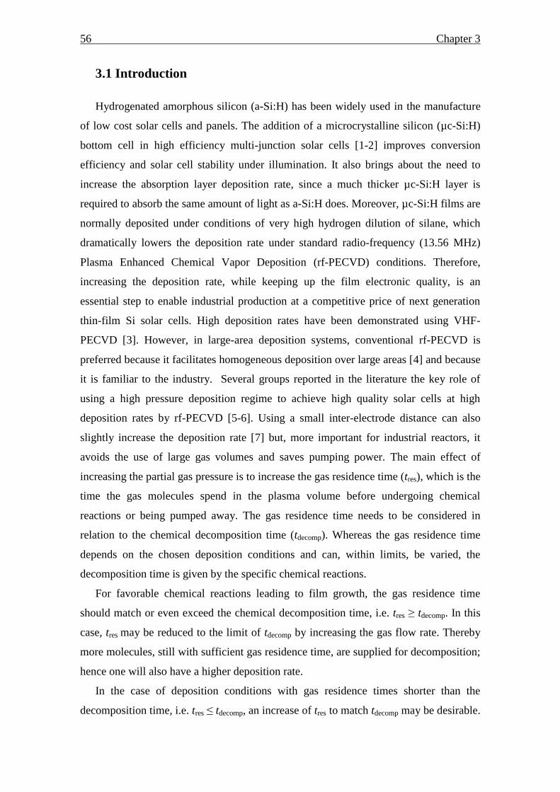
56 Chapter 3
3.1 Introduction
Hydrogenated amorphous silicon (a-Si:H) has been widely used in the manufacture
of low cost solar cells and panels. The addition of a microcrystalline silicon (µc-Si:H)
bottom cell in high efficiency multi-junction solar cells [1-2] improves conversion
efficiency and solar cell stability under illumination. It also brings about the need to
increase the absorption layer deposition rate, since a much thicker µc-Si:H layer is
required to absorb the same amount of light as a-Si:H does. Moreover, µc-Si:H films are
normally deposited under conditions of very high hydrogen dilution of silane, which
dramatically lowers the deposition rate under standard radio-frequency (13.56 MHz)
Plasma Enhanced Chemical Vapor Deposition (rf-PECVD) conditions. Therefore,
increasing the deposition rate, while keeping up the film electronic quality, is an
essential step to enable industrial production at a competitive price of next generation
thin-film Si solar cells. High deposition rates have been demonstrated using VHF-
PECVD [3]. However, in large-area deposition systems, conventional rf-PECVD is
preferred because it facilitates homogeneous deposition over large areas [4] and because
it is familiar to the industry. Several groups reported in the literature the key role of
using a high pressure deposition regime to achieve high quality solar cells at high
deposition rates by rf-PECVD [5-6]. Using a small inter-electrode distance can also
slightly increase the deposition rate [7] but, more important for industrial reactors, it
avoids the use of large gas volumes and saves pumping power. The main effect of
increasing the partial gas pressure is to increase the gas residence time (tres), which is the
time the gas molecules spend in the plasma volume before undergoing chemical
reactions or being pumped away. The gas residence time needs to be considered in
relation to the chemical decomposition time (tdecomp). Whereas the gas residence time
depends on the chosen deposition conditions and can, within limits, be varied, the
decomposition time is given by the specific chemical reactions.
For favorable chemical reactions leading to film growth, the gas residence time
should match or even exceed the chemical decomposition time, i.e. tres ≥ tdecomp. In this
case, tres may be reduced to the limit of tdecomp by increasing the gas flow rate. Thereby
more molecules, still with sufficient gas residence time, are supplied for decomposition;
hence one will also have a higher deposition rate.
In the case of deposition conditions with gas residence times shorter than the
decomposition time, i.e. tres ≤ tdecomp, an increase of tres to match tdecomp may be desirable.

High-rate deposition of nano-crystalline silicon thin films on plastics 57
This can be easily achieved by increasing the pressure. As a consequence, the
probability of more molecules being decomposed rises, and basically leads to a higher
deposition rate. However, higher pressures imply higher collision rates, which may also
result in gas phase reactions, and hence in powder formation. Thereby fewer reacted
species reach the growing film, and this, in turn, tends to lower the deposition rate. In
case of relatively small electrode spacings, the probability of chemical decomposition at
the growing film surface, rather than in the plasma volume, may be higher and, thus, the
deposition rate will be less adversely affected by powder formation.
Thin-film photovoltaics can only compete in a market dominated by highly efficient
c-Si technology if they offer very low price and/or focus on niche markets. One way to
achieve both goals is to use flexible, inexpensive plastic substrates which moreover lend
themselves to inline high throughput fabrication processes.
This chapter describes the optimization of a-Si:H and µc-Si:H intrinsic and doped
layers deposited by rf-PECVD on plastic (PEN) at 150 ºC. A small (1.2 cm) inter-
electrode distance is used. Focus is placed in the influence of deposition pressure and
power coupled to the plasma, on the deposition rate and film electronic quality.
3.2 Experimental details
Hydrogenated amorphous silicon and µc-Si:H thin films are deposited by rf-PECVD
on 125 µm thick plastic substrates (PEN, polyethylene naphthalate) using SiH4 diluted
in H2. Hydrogen dilution is defined as HD = [FH2/(FSiH4 + FH2)]100%, where F’s are
gas flow rates, and values between 96 and 99% are used. Substrates are clamped to the
top earthed electrode, placed 1.2 cm from the bottom powered electrode, in a parallel
plate capacitor configuration, and heated to the deposition temperature Tsub = 150ºC.
Three HD-series of films are prepared at deposition pressure pw = 1.5, 3 and 6 Torr. In
all series rf-power, Prf, is 10 W, corresponding to a power density of 350 mW/cm2. The
6 Torr series is repeated using Prf = 20 W (power density = 700 mW/cm2).
Deposition rate, rd, is derived from the thickness obtained by analysis of interference
fringes in the UV-visible-NIR transmittance spectra and confirmed by profilometry.
Film structure is studied by Raman and FTIR spectroscopy. The Raman crystalline
fraction, Xc, and crystallite size, dnc, of the films are calculated according to reference
[8], as described in section 2.5.1. For the amorphous films, the bond angle deviation Δθ

58 Chapter 3
is related to the full width at half maximum (FWHM) Г of the TO peak centered at 480
cm-1
. Room temperature dark conductivity, σdk, and secondary photoconductivity, σph,
are measured between coplanar Al contacts 6 mm long with 1 mm gap. Urbach tails and
deep defect absorption are obtained from Constant Photocurrent Measurements (CPM).
3.3 Structural properties
Raman spectra of films deposited under HD = 96, 97, 98 and 98.5% at pw = 1.5 Torr
[fig. 3.1(a)], 3 Torr [fig. 3.1(b)] and 6 Torr [fig. 3.1(c)] show that for HD = 98% their
structure is amorphous at 6 Torr and microcrystalline at 3 and 1.5 Torr, with Xc = 34%
and 56%, respectively. It is concluded that the hydrogen induced amorphous-to-
microcrystalline transition (a→µc) requires a progressively higher HD as the pressure is
increased from 1.5 to 3 and 6 Torr. At 6 Torr the a→µc transition occurs only for HD =
98.5% after increasing rf-power to 20 W [fig.3.1(c)]. Films deposited at 6 Torr and Prf =
10 W (shown only in fig. 3.2) are amorphous up to extreme HD = 99% at which the
a→µc occurs (Xc~70%). This finding can be correlated with results in literature that
show, in high H2 diluted silane plasmas, a progressive shift in concentration of positive
ion species from H+ to SiHm
+ as pressure increases in the range 0.1-10 Torr [9]. In fact,
it has been shown that with the same type of plasma it is only the presence or absence of
ions impinging at the growing film surface that determines whether it is amorphous or
microcrystalline. It has to be emphasised that a high ionic concentration close to the
film surface is not a problem for the film quality but it is the energy of those ions that
may pose a problem [10]. In fact, a high ion flux with low kinetic energy obtained at
high frequencies gives rise to enhanced surface diffusion of impinging species, even at a
low substrate temperature, which is a necessary condition for good crystallinity. It is
found that suppression of the ion energy is more effective for improving crystallinity,
specially at high growth rates, and it is speculated that hydrogen ions etch the a-Si:H,
whereas atomic hydrogen promotes the Si-network [11].
For all pressures and rf-powers studied the a→µc occurs abruptly, within a 0.5-1%
interval in the HD scale. Microcrystalline samples deposited at 6 Torr have lower sized
(< 5 nm) Si microcrystals, when compared to the films deposited at 1.5 and 3 Torr
(crystallite size ~ 7 nm). This effect is clearly seen in the Raman spectra by the red shift
of the crystalline peak.
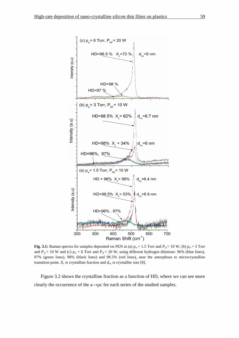
High-rate deposition of nano-crystalline silicon thin films on plastics 59
Fig. 3.1: Raman spectra for samples deposited on PEN at (a) pw = 1.5 Torr and Prf = 10 W, (b) pw = 3 Torr
and Prf = 10 W and (c) pw = 6 Torr and Prf = 20 W, using different hydrogen dilutions: 96% (blue lines),
97% (green lines), 98% (black lines) and 98.5% (red lines), near the amorphous to microcrystalline
transition point. Xc is crystalline fraction and dnc is crystallite size [8].
Figure 3.2 shows the crystalline fraction as a function of HD, where we can see more
clearly the occurrence of the a→µc for each series of the studied samples.
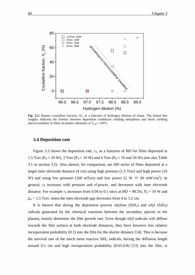
60 Chapter 3
96.0 96.5 97.0 97.5 98.0 98.5 99.0
0
20
40
60
80
amorphous-to-m
icrocrystalline transition
Hydrogen dilution (%)
Cry
sta
llin
e f
ractio
n,
Xc (
%)
1.5Torr, 10W
3Torr, 10W
6Torr, 10W
6Torr, 20W
Fig. 3.2: Raman crystalline fraction, Xc, as a function of hydrogen dilution of silane. The dotted line
roughly indicates the frontier between deposition conditions yielding amorphous and those yielding
microcrystalline Si films on plastic substrates at Tsub= 150ºC.
3.4 Deposition rate
Figure 3.3 shows the deposition rate, rd, as a function of HD for films deposited at
1.5 Torr (Prf = 10 W), 3 Torr (Prf = 10 W) and 6 Torr (Prf = 10 and 20 W) (see also Table
3.1 in section 3.5). Also shown, for comparison, are HD series of films deposited at a
larger inter electrode distance (4 cm) using high pressure (1.5 Torr) and high power (10
W) and using low pressure (160 mTorr) and low power (2 W 60 mW/cm2). In
general, rd increases with pressure and rf-power, and decreases with inter electrode
distance. For example rd increases from 0.04 to 0.1 nm/s at HD = 98.5%, Prf = 10 W and
pw = 1.5 Torr, when the inter electrode gap decreases from 4 to 1.2 cm.
It is known that during the deposition process silylene (SiH2) and silyl (SiH3)
radicals generated by the chemical reactions between the secondary species in the
plasma, mainly determine the film growth rate. Even though silyl radicals will diffuse
towards the film surface at both electrode distances, they have however less relative
incorporation probability (0.1) into the film for the shorter distance [14]. This is because
the survival rate of the much more reactive SiH2 radicals, having the diffusion length
around 0.5 cm and high incorporation probability (0.65-0.8) [13] into the film, is

High-rate deposition of nano-crystalline silicon thin films on plastics 61
favoured by the short distance between the electrodes. Possibly the silylene radicals are
therefore playing an important role in increasing the deposition rate when the inter
electrode gap is reduced.
95.0 95.5 96.0 96.5 97.0 97.5 98.0 98.5 99.00.0
0.1
0.2
0.3
0.4
0.5
0.6
am
orp
hous-
to-m
icro
crys
talli
ne tr
ansi
tion
1.2 cm, 6 Torr, 20 W
1.2 cm, 6 Torr, 10 W
1.2 cm, 3 Torr, 10 W
1.2 cm, 1.5 Torr, 10 W
4 cm, 1.5 Torr, 10 W
4 cm, 0.160 Torr, 2 W
De
po
sitio
n r
ate
, r d
(n
m/s
)
Hydrogen dilution (%)
Fig. 3.3: Deposition rate as a function of HD for films deposited on plastic substrates at different
pressures (0.160, 1.5, 3, and 6Torr) and rf-powers (2, 10 and 20 W).
In figure 3.3, data points with abscissa HD = 98.5% correspond, with one exception
at 6 Torr (10 W), to microcrystalline films with Xc > 50%. Deposition rate increases
approximately 10-fold from bottom to top, i.e. from 0.04 nm/s at 1.5 Torr (10 W) to
0.38 nm/s at 6 Torr (20 W). The transition from an amorphous film at pw = 6 Torr (10
W) to a highly crystalline one (Xc = 72%) at pw = 6 Torr (20 W) might correspond to the
threshold of a high-pressure SiH4 depletion regime, thus inhibiting the H annihilation
reaction (H+SiH4 → H2+SiH3) and consequently increasing atomic H concentration,
which induces the a→µc transition. It is found in ref. [14] that this high rate deposition
regime for µc-Si:H preserves the high electronic quality of the films.
3.5 Opto-electronic properties
Table 3.1 summarizes important optical and electronic properties of selected
samples.
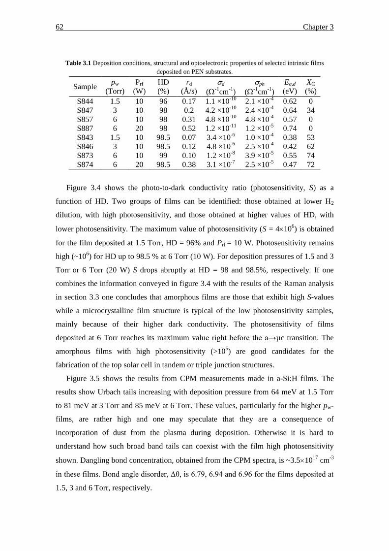
62 Chapter 3
Table 3.1 Deposition conditions, structural and optoelectronic properties of selected intrinsic films
deposited on PEN substrates.
Sample pw
(Torr)
Prf
(W)
HD
(%)
rd
(Å/s)
d
(-1
cm-1
)
ph
(-1
cm-1
)
Ea,d
(eV)
XC
(%)
S844 1.5 10 96 0.17 1.1 ×10⁻¹⁰
2.1 ×10⁻⁴
0.62 0
S847 3 10 98 0.2 4.2 ×10⁻¹⁰
2.4 ×10⁻⁴
0.64 34
S857 6 10 98 0.31 4.8 ×10⁻¹⁰
4.8 ×10⁻⁴
0.57 0
S887 6 20 98 0.52 1.2 ×10⁻¹¹
1.2 ×10⁻⁵
0.74 0
S843 1.5 10 98.5 0.07 3.4 ×10⁻⁶
1.0 ×10⁻⁴
0.38 53
S846 3 10 98.5 0.12 4.8 ×10⁻⁶
2.5 ×10⁻⁴
0.42 62
S873 6 10 99 0.10 1.2 ×10⁻⁸
3.9 ×10⁻⁵
0.55 74
S874 6 20 98.5 0.38 3.1 ×10⁻⁷
2.5 ×10⁻⁵
0.47 72
Figure 3.4 shows the photo-to-dark conductivity ratio (photosensitivity, S) as a
function of HD. Two groups of films can be identified: those obtained at lower H2
dilution, with high photosensitivity, and those obtained at higher values of HD, with
lower photosensitivity. The maximum value of photosensitivity (S = 4106) is obtained
for the film deposited at 1.5 Torr, HD = 96% and Prf = 10 W. Photosensitivity remains
high (~106) for HD up to 98.5 % at 6 Torr (10 W). For deposition pressures of 1.5 and 3
Torr or 6 Torr (20 W) S drops abruptly at HD = 98 and 98.5%, respectively. If one
combines the information conveyed in figure 3.4 with the results of the Raman analysis
in section 3.3 one concludes that amorphous films are those that exhibit high S-values
while a microcrystalline film structure is typical of the low photosensitivity samples,
mainly because of their higher dark conductivity. The photosensitivity of films
deposited at 6 Torr reaches its maximum value right before the a→µc transition. The
amorphous films with high photosensitivity (>105) are good candidates for the
fabrication of the top solar cell in tandem or triple junction structures.
Figure 3.5 shows the results from CPM measurements made in a-Si:H films. The
results show Urbach tails increasing with deposition pressure from 64 meV at 1.5 Torr
to 81 meV at 3 Torr and 85 meV at 6 Torr. These values, particularly for the higher pw-
films, are rather high and one may speculate that they are a consequence of
incorporation of dust from the plasma during deposition. Otherwise it is hard to
understand how such broad band tails can coexist with the film high photosensitivity
shown. Dangling bond concentration, obtained from the CPM spectra, is ~3.51017
cm-3
in these films. Bond angle disorder, Δθ, is 6.79, 6.94 and 6.96 for the films deposited at
1.5, 3 and 6 Torr, respectively.
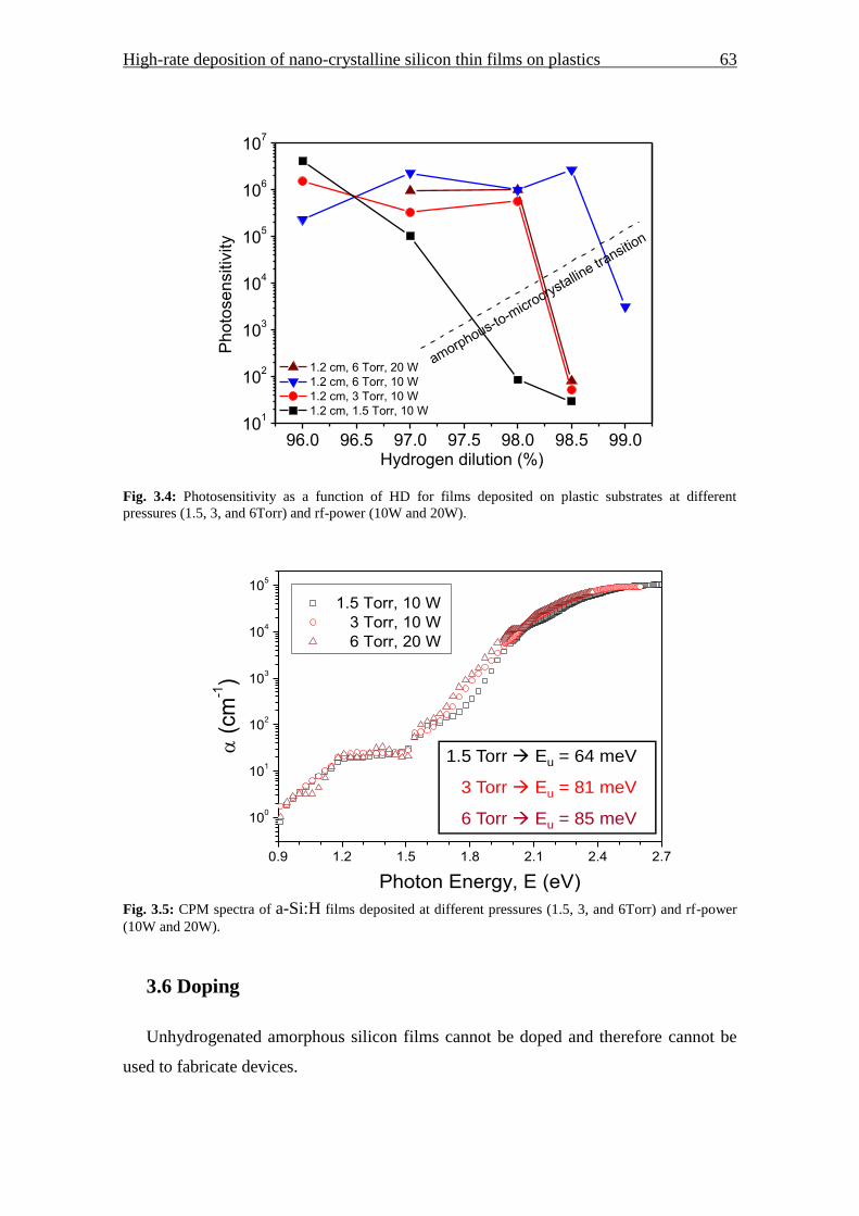
High-rate deposition of nano-crystalline silicon thin films on plastics 63
96.0 96.5 97.0 97.5 98.0 98.5 99.010
1
102
103
104
105
106
107
amorphous-to-m
icrocrystalline tra
nsition
1.2 cm, 6 Torr, 20 W
1.2 cm, 6 Torr, 10 W
1.2 cm, 3 Torr, 10 W
1.2 cm, 1.5 Torr, 10 W
Hydrogen dilution (%)
Ph
oto
se
nsitiv
ity
Fig. 3.4: Photosensitivity as a function of HD for films deposited on plastic substrates at different
pressures (1.5, 3, and 6Torr) and rf-power (10W and 20W).
Fig. 3.5: CPM spectra of a-Si:H films deposited at different pressures (1.5, 3, and 6Torr) and rf-power
(10W and 20W).
3.6 Doping
Unhydrogenated amorphous silicon films cannot be doped and therefore cannot be
used to fabricate devices.
0.9 1.2 1.5 1.8 2.1 2.4 2.7
100
101
102
103
104
105
(
cm
-1)
Photon Energy, E (eV)
1.5 Torr, 10 W
3 Torr, 10 W
6 Torr, 20 W
1.5 Torr Eu = 64 meV
3 Torr Eu = 81 meV
6 Torr Eu = 85 meV

64 Chapter 3
On the other hand, amorphous silicon layers deposited by PECVD from silane
contain hydrogen atoms, which passivate a large part of their dangling bonds; such
films can be doped by adding phosphine (PH3) or diborane (B2H6) to the silane in order
to obtain n- and p-type layers, respectively [15]. What one experimentally finds is,
however, that the doping efficiency of phosphorous and boron atoms in hydrogenated
amorphous silicon is much lower than in crystalline silicon. As the dopant level
increases, the doping efficiency decreases even more. It is not possible by doping to
push the Fermi level EF to meet the band edges EC and EV.
This is accounted for in the theory of doping developed by R. Street for amorphous
silicon [16] by the concept of compensation. It says that most of the active dopants
(which are less than 1% of the P-content in the film, the remaining 99% staying in the
3-fold coordination configuration) are stabilized in the host four-fold configuration by
electron transfer to a midgap localized defect states, where they do not contribute to the
electrical conductivity. The process of doping itself generates deep defects in
amorphous silicon, at a rate of almost one dangling bond (DB) by active dopant atom
incorporated. In fact this number is 0.9 DB per 4-fold coordinated P-atom (even less
when doping with Boron). As a consequence, for n-type doping, there is a slight excess
of electrons relative to DBs and these electrons in excess are the only ones responsible
for shifting the Fermi level towards the band edge. From all the electrons occupying
band edge states, only a small fraction occupies states above the mobility edge: these
are the only carriers that contribute to increase the electrical conductivity.
Despite all this, it is possible to increase the dark conductivity of the films by adding
a dopant gas to the silane plasma; however, after reaching a certain doping level this
effect stops: it is not possible to reach conductivities much higher than 10-2
Ω-1
cm-1
for
doped a-Si:H films [17]. The doped conductivity of p-type films is normally lower than
that of n-type films due to the lower drift mobility of holes in the valence bandtail than
of electrons in the conduction bandtail since the first is broader than the latter.
It is found that the doping process in µc-Si:H is a mixture of the phenomena
observed in a-Si:H and in c-Si. For low doping levels, of the order of the defect density
in the material, i.e. around 1016
-1017
cm-3
electrons or holes from the dopant atoms first
have to fill up these defect states, just as in a-Si:H. For higher doping levels we observe
a 1:1 relationship between the built-in doping atoms and carrier density, i.e. we have a
substitutional doping process in the crystalline phase of µc-Si:H similar to that in c-Si.
In particular, one does not observe any self-compensation effect of the doping process

High-rate deposition of nano-crystalline silicon thin films on plastics 65
by thermal equilibrium between four-fold coordinated dopant states and defects. As a
result, one can obtain considerably higher conductivities and carrier densities in µc-
Si:H, as compared with a-Si:H: it is possible to reach conductivities as high as 102 Ω
-
1cm
-1 for n- or p-type layers [15].
Phosphine (PH3) or diborane (B2H6) are added to the reactive gas mixture, while
keeping up the deposition conditions that yielded the best µc-Si:H (higher XC) and a-
Si:H films (higher S) to obtain n- or p-type films, respectively. Results can be seen in
figure 3.6 where σdk is plotted as a function of hydrogen dilution for films deposited at
pw = 1.5, 3 and 6 Torr, with Prf = 10 W (350 mW/cm2). For n-type films R, defined as
the dopant-gas-to-silane flow rate ratio, is kept constant and equal to 2.5. For p-type
films R is varied in the interval [0.5, 2.5] (R = 0.5, 1, 1.5, 2 and 2.5).
Fig. 3.6: Dark conductivity as a function of hydrogen dilution for p- and n-doped films deposited on PEN
at different pressures (1.5, 3, and 6 Torr) and doping ratios (0.5, 1 and 2.5).
Highly conductive µc-Si:H n-type films were obtained at 1.5 and 3 Torr, with
conductivities of 0.7 and 8 Ω-1
cm-1
, respectively. At 6 Torr it was not possible to obtain
highly doped films because their structure was strongly amorphized by the dopants [18]
and the σdk was around 10-2
Ω-1
cm-1
(Ea,dk = 140 meV). The most strongly doped n-type
66 Chapter 3
a-Si:H films were obtained at 1.5 and 3 Torr, with σdk around 10-3
Ω-1
cm-1
(Ea,dk ~ 0.25
eV).
Highly conductive µc-Si:H p-type films with σdk ~ 1 Ω-1
cm-1
(Ea,dk ~ 30 meV) were
obtained at 1.5 and 3 Torr, using R = 1 and 0.5, respectively. At 6 Torr it was not
possible to obtain p-type doped microcrystalline films because of the amorphization
induced by the dopant atoms. The highest p-type conductivity obtained for a-Si:H films
was ~ 510-7
Ω-1
cm-1
(Ea,dk ~ 0.5 eV) for R = 2.5, obtained at all pressures studied.
3.7 Conclusions
The deposition rate of both a-Si:H and µc-Si:H thin films can be increased
consistently by: 1) decreasing the inter electrode distance, 2) increasing the deposition
pressure, and 3) increasing the rf-power. The deposition rate decreases as the HD
increases in all deposition conditions. For each pressure and rf-power used, there is a
value of hydrogen dilution of silane for which the films undergo an amorphous-to-
microcrystalline phase transition. The exact concentration of H2 required for this
transition to occur is a function of the deposition parameters and it increases when the
working pressure increases, keeping other parameters constant. At 6 Torr it is necessary
to increase simultaneously HD and rf‐power in order to obtain µc-Si:H films. The films
obtained under such conditions are deposited at the highest microcrystalline deposition
rate (rd = 0.38 nm/s). The films with high photosensitivity (>105) are amorphous. The
best µc-Si:H have photosensitivity around 102. The best mixed phase film is obtained at
6 Torr, 20 W and has photosensitivity in excess of 103. n- and p-type µc-Si:H films are
obtained with σdk = 7.8 and 0.87 Ω-1
cm-1
, respectively. At 6 Torr, it is not possible to
obtain highly doped microcrystalline films. n-type conductivity is 10-3
Ω-1
cm-1
while p-
type σdk= 510-7
Ω-1
cm-1
.

High-rate deposition of nano-crystalline silicon thin films on plastics 67
References
[1] V. Shah, J. Meier, E. Vallat-Sauvain, N. Wyrsch, U. Kroll, C. Droz and U. Graf, Sol.
Energy Mater. Sol. Cells, 78 (2003) p. 469.
[2] S. Guha and J. Yang, J. Non-Cryst. Solids, 352 (2006) p. 1917.
[3] O. Vetterl, F. Finger, R. Carius, P. Hapke, L. Houben, O. Kluth, A. Lambertz, A. Mück,
B. Rech and H. Wagner, Sol. Energy Mater. Sol. Cells, 62 (2000) p. 97.
[4] U. Kroll, D. Fischer, J. Meier, L. Sansonnens, A. Howling and A. Shah, Mater. Res.
Soc. Symp. Proc. 557 (1999) p. 121.
[5] L. Guo, M. Kondo, M. Fukawa, K. Saitoh and A. Matsuda, Jpn. J. Appl. Phys. 37
(1998) p. L1116.
[6] B. Rech, T. Roschek, T. Repmann, J. Müller, R. Schmitz and W. Appenzeller, Thin
Solid Films, 427 (2003) p. 157.
[7] Y. Fukuda, Y. Sakuma, C.H. Fukai, Y. Fujimura, K. Azuma and H. Shirai, Thin Solid
Films, 386 (2001) p. 256.
[8] T. Kaneko, M. Wakagi, K. Onisawa, and T. Minemura, Appl. Phys. Lett., 64 (1994) p.
1865.
[9] S. Nunomura and M. Kondo, Appl. Phys. Lett. 93 (2008) p. 231502.
[10] J. Perrin, M. Shiratani, P. Kae-Nune, H. Videlot, J. Jolly and J. Guillon, J. Vac. Sci.
Technol. A, 16 (1998) p. 278.
[11] H. Keppner, U. Kroll, P. Torres, J. Meier, D. Fischer, M. Goetz, T. Tscharner, A. Shah,
In Proceedings of 25th IEEE Photovoltaic Specialist Conference, 669 (1996).
[12] J. K. Rath, Solar Energy Materials and Solar Cells, 76 (2003) p. 431.
[13] M. Hertl and J. Jolly, J. Phys. D: Appl. Phys. 33 (2000) p. 381.
[14] M. Kondo, M. Fukawa, L. Guo and A. Matsuda, J. Non-Cryst. Solids, 266 (2000) p. 84.
[15] A. Shah, ed., Thin-film Silicon Solar Cells, First edition, EPFL Press (2010).
[16] M. Stutzmann, D. K. Biegelsen, R. A. Street, Phys. Rev. B35 (1987) p. 5666.
[17] W.E. Spear, P.G. LeComber, Sol. State Comm. 17 (1975) p. 1193.
[18] P. Alpuim, M. Andrade, V. Sencadas, M. Ribeiro, S.A. Filonovich, S. Lanceros-
Mendez, Thin Solid Films, 515 (2007) p. 7658.

68 Chapter 3
Chapter 4
4 Amorphous silicon solar cells on flexible substrates
In order to improve the transparent contact layer in amorphous silicon solar cells
fabricated on low-temperature plastic substrates, Al and Ga doped ZnO films were
deposited at room temperature on plastic and glass and their optical, electronic and
structural properties were correlated and optimized. Selected deposition conditions
resulting from the study described in the previous chapter were used to fabricate
amorphous silicon solar cells at a substrate temperature of 150 ºC on PEN/TCO, in the
superstrate p-i-n configuration. The efficiency is around 5%, limited by low current
density and low fill factor. Amorphous silicon solar cells with efficiencies around 6.5%
were also fabricated in the substrate n-i-p configuration on PI foils at a substrate
temperature of 200 ºC. Aiming to explore light trapping effects, plastic substrates were
laser textured and their haze, total transmittance and reflectance were compared with
those of untextured substrates. Although the haze increased dramatically, from 1.7 to
78.9%, the total transmittance of PET coated with ZnO:Ga decreased from 83.9%, in
the untextured substrate, to 58.5% in the textured PET. The haze in reflected light of
PET coated with Al increased from 4.3% to 66.2% after texturing but the total
reflectance decreased from 70.1% to 36.8%. Therefore these substrates were not used
for solar cell fabrication.
70 Chapter 4
4.1 Introduction
Single junction amorphous silicon solar cells were fabricated on flexible plastic
substrates in p-i-n configuration on PEN at 150 ºC, and in n-i-p configuration on PI at
200 ºC.
Another issue for fabrication on plastics is the deposition of the transparent and
conductive oxide (TCO) used as contact window layer in a-Si:H solar cells. These
layers are typically made on glass, at high temperature (> 150 ºC) that is not compatible
with plastic substrates. In this study, doped zinc oxide is deposited at room temperature
directly on plastic. Aluminium and gallium are used as dopants and their effect on the
structural, optical and electronic properties of the TCO are studied.
In order to increase the relatively low efficiency of a-Si:H solar cells it is crucial to
develop light-trapping schemes that largely increase the optical path length inside the
absorbing layer [1]. Excimer laser texturization of plastic substrates was carried out and
the resulting optical characteristics of the substrates were characterized.
4.2 Experimental details
ZnO:Ga (GZO) and ZnO:Al (AZO) thin films are deposited at room temperature in
vacuum under an Ar atmosphere with a base pressure of 210-6
Torr by DC magnetron
sputtering keeping a target-to-substrate distance constant at 8 cm in all runs. For GZO
deposition a 2-inch ZnO:Ga target, (zinc oxide/gallium, 95.5/4.5 wt.%), a working
pressure of 4 mTorr and a target current density of 4.9 mA cm-2
have been used and a
deposition rate of 0.47 nm/s is obtained. For AZO deposition a 4-inch ZnO:Al target,
(zinc oxide/aluminium, 98.0/2.0 wt.%), a working pressure of 3 mTorr and a target
current density of 2.5 mA cm-2
have been used and a deposition rate of 0.48 nm/s is
obtained.
The texturing of plastic substrates, consisting of ablation at laser irradiation above
the material damage threshold, is performed on polyester films (polyethylene
terephthalate, PET) with thickness of 125 µm. Substrates are cleaned in ethanol in an
ultrasonic bath for 10 min followed by 10 min in water. The light source is ArF Excimer
Laser (193 nm). Fluence is controlled by an attenuator (Lasoptics) followed by imaging
using a fly’s eye homogenizer (EX-HS-700D) with 650 mm spherical focusing lens.
Amorphous silicon solar cells on flexible substrates 71
The sample is positioned on a holder with single axis servo motor at the focus of the
homogenizer allowing movement in direction perpendicular to the incident beam. Laser
repetition rate is always 1 Hz, fluence is varied as follows: 50, 60 and 70 mJ/cm2, with
the corresponding velocity 0.5, 0.5 and 1 mm/s.
Optical properties of the textured plastics substrates are measured in a dual beam
Shimadzu spectrophotometer set-up in transmission and reflection modes. In specular
transmittance, reference sample (non-treated PET) and the studied sample (laser treated
PET) are put into two different substrate holders. The light beam of wavelengths
ranging from 250-900 nm is split in two beams that simultaneously passed through each
sample. The difference between the reference beam and the beam coming from the
sample is recorded in the form of a spectrum. Diffuse transmittance measurements are
performed using an integrating sphere. Integrating spheres are shells coated with a
highly reflective material such as barium sulfate. The sphere has entrance and exit
apertures for incident and emergent light, respectively. Detectors are positioned directly
under or over an aperture in the bottom or top of the sphere, respectively.
Single junction p-i-n superstrate solar cells are fabricated at 150 ºC by rf-PECVD
(deposition system described in section 2.3.1) on 125 µm-thick PEN substrate covered
with GZO. Table 4.1 shows the deposition parameters of the p-i-n junction. To
complete the solar cell on plastic, thermally evaporated Al contacts are used, also acting
as back reflectors. The substrate area is 3×3 cm2 or 1.5×3.0 cm
2 and the area of the solar
cells, defined by using a shadow mask during Al back contact deposition, is 0.126 cm2
or 0.0314 cm2. Selected solar cells are annealed at 150 ºC in vacuum for 30 minutes to
one hour.
Table 4.1: Deposition conditions for Si layers used in the solar cells fabrication.
Layer Tsub.
(ºC)
H2 dilution
(%)
PRF
(mW/cm2)
pw
(Torr)
FPH3/FSiH4
(%)
FB2H6/FSiH4
(%)
intrinsic 150 96 350 1.5
buffer a-Si:H 100 97 175 0.15
n-type 150 96 350 1.5 2.5
p-type 150 98.5 175 1.5 2.5
Amorphous silicon n-i-p substrate solar cells are fabricated on 125 µm-thick
polyimide foils. The solar cells are prepared on 10×10 cm² foils. The substrate holder
used for the fabrication procedure is a 10×10 cm² stainless steel sandwich mask

72 Chapter 4
consisting of a back plate and a frame with 6 apertures of 4×2.3 cm² each, as shown in
fig. 4.1.
(a) (b) (c)
Fig. 4.1: Sandwich mask used to hold the polyimide substrate during depositions. a) back plate, b) frame
and c) PI foil fixed on the back plate.
The substrates are covered with a thermally evaporated 700 nm Ag layer and an 80
nm sputtered ZnO:Ga, both deposited at room temperature. The thin film silicon layers
are deposited in n-i-p sequence by standard rf-PECVD (13.56 MHz) using the cluster
tool deposition system described in section 2.3.2. The substrate temperature is 200ºC for
intrinsic and doped layers. The power density and working pressure for deposition of
intrinsic and doped layers are 42 mW/cm2 and 1.2 Torr, respectively. The front
transparent contacts made of 70 nm thick AZO layers are prepared by radio-frequency
(RF) magnetron sputtering at 150°C using a ZnO:Al target (98/2 wt.%) in an argon
atmosphere. The individual solar cells with an area of 1×1 cm2 are defined by using a
shadow mask during AZO deposition on the 10×10 cm² substrate. Front metal finger
electrodes are prepared by silver evaporation. Finally, standard annealing procedure of
finished solar cells is performed in air at 160°C for 30 minutes. The complete device
layer sequence is: PI/Ag/GZO/n-i-p/AZO. For comparison solar cells are also deposited
on glass substrates with corresponding layer sequences.
4.3 Doped ZnO films
Figure 4.2 shows the Raman spectra of ZnO films with thicknesses of ~700 nm
doped with Al (top) and with Ga (bottom). The optical transmittance was higher than
80% in both films. The Raman characteristic 437 cm−1
peak of ZnO wurtzite structure,
assigned to the non-polar optical phonon mode (E2-high) is present in both spectra.
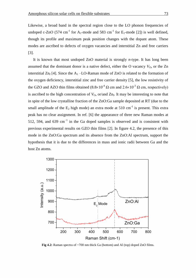
Amorphous silicon solar cells on flexible substrates 73
Likewise, a broad band in the spectral region close to the LO phonon frequencies of
undoped c-ZnO (574 cm-1
for A1-mode and 583 cm-1
for E1-mode [2]) is well defined,
though its profile and maximum peak position changes with the dopant atom. These
modes are ascribed to defects of oxygen vacancies and interstitial Zn and free carriers
[3].
It is known that most undoped ZnO material is strongly n-type. It has long been
assumed that the dominant donor is a native defect, either the O vacancy VO, or the Zn
interstitial ZnI [4]. Since the A1 –LO-Raman mode of ZnO is related to the formation of
the oxygen deficiency, interstitial zinc and free carrier density [5], the low resistivity of
the GZO and AZO thin films obtained (8.810-4
Ω cm and 2.610-3
Ω cm, respectively)
is ascribed to the high concentration of VO, or/and ZnI. It may be interesting to note that
in spite of the low crystalline fraction of the ZnO:Ga sample deposited at RT (due to the
small amplitude of the E2 high mode) an extra mode at 510 cm-1
is present. This extra
peak has no clear assignment. In ref. [6] the appearance of three new Raman modes at
512, 594, and 639 cm−1
in the Ga doped samples is observed and is consistent with
previous experimental results on GZO thin films [2]. In figure 4.2, the presence of this
mode in the ZnO:Ga spectrum and its absence from the ZnO:Al spectrum, support the
hypothesis that it is due to the differences in mass and ionic radii between Ga and the
host Zn atoms.
200 300 400 500 600 700 800
700
800
900
1000
1100
1200
1300
E2 Mode
Inte
nsity (
a.u
.)
Raman Shift (cm-1)
ZnO:Ga
ZnO:Al
Fig 4.2: Raman spectra of ~700 nm thick Ga (bottom) and Al (top) doped ZnO films.

74 Chapter 4
4.4 p-i-n superstrate solar cells on PEN
As-deposited p-i-n solar cells showed conversion efficiency (η) between 1-3% under
AM 1.5 conditions. Upon annealing at 150oC for 30 minutes to 1 hour in vacuum,
conversion efficiency improved. Figure 4.3 shows the I-V curves of two p-i-n diode
amorphous silicon solar cells deposited on PEN/GZO. The two curves correspond to
solar cells differing in two respects. Firstly, their absorbing layers are different – SC88
has a 400 nm thick i-layer deposited by rf-PECVD (HD = 96%) and SC91 has a 350 nm
thick i-layer deposited by HWCVD (HD = 50%). Secondly, their p-layers, both
deposited by rf-PECVD, have different optical bandgaps – 1.89 eV for SC88 and 1.76
eV for SC91. Both cells have a 9 nm buffer layer inserted between the p and i-layers in
order to prevent electron back diffusion into the p-layer and to protect the p-layer from
atomic hydrogen attack during the i-layer deposition. This is crucial when depositing
the i-layer by HWCVD, since the high concentration of atomic hydrogen produced by
decomposition of SiH4 and H2 at the filament readily attacks the boron-doped layer and
will destroy it in the absence of the protective buffer layer.
The parameters derived from the I-V plot are given in table 4.2. The HWCVD cell
has a higher short-circuit current (JSC = -12.7 mA/cm2), probably due to the thinner i-
layer, which favors a fully depleted i-layer and an enhanced built-in electric field
resulting in a higher carrier collection efficiency (see section 1.1.2). The rf-PECVD cell
has higher Voc (= 0.830 V), because the i-layer has the highest photosensitivity (see fig.
3.4) and the p-layer has the highest Eopt of the two. Solar cell SC88 has a higher shunt
resistance under AM1.5 illumination (see table 4.2) which, together with its higher Voc
give a slightly better fill factor (FF = 54.2%) when compared to SC91 (FF = 51.0%).
In order to assess where the main conversion losses occur, external quantum
efficiency (EQE) measurements are performed under: i) no bias; ii) a small reverse bias
(-1V); and iii) a forward bias corresponding to the maximum operating power point
(0.5-0.6V). Figure 4.4 shows the results for the solar cell SC91, with i-layer by HW.
The EQE results for SC88 (i-layer by rf-PECVD) are not displayed here but they are
essentially identical to those shown in fig. 4.4. Therefore, the discussion and main
conclusions that will follow can also be applied grosso modo to solar cell SC88 as well.
The EQE of a calibrated solar cell (R-SC) deposited on ITO/Glass substrate at 250 ºC is
also plotted as a reference.

Amorphous silicon solar cells on flexible substrates 75
-1.0 -0.8 -0.6 -0.4 -0.2 0.0 0.2 0.4 0.6 0.8 1.0-15
-10
-5
0
5
10SC91
i-layer by HWSC88
i-layer by RFFF= 51.0 %
Jsc= -12.7 mA/cm2
Voc= 0.699 V
EFF= 4.53 %
Cu
rre
nt
De
nsity (
mA
/cm
2)
Voltage (V)
FF= 54.2 %
Jsc= -11.2 mA/cm2
Voc= 0.830 V
EFF= 5.03 %
PEN \ GZO \ p-RF \ b-RF(9nm) \ i \ n-RF
Fig. 4.3: AM1.5 I-V curves of p-i-n solar cells deposited on plastic (PEN).
Figure 4.4 shows that the maximal values of EQE (0.7) fall short of the value of 0.8
charge carriers collected per incident photon, which is typical of good a-Si:H solar cells.
It is apparent that one main difference between the R-SC and the flexible solar cell is
the response in the long wavelength part of the spectrum, which could be explained by a
reduced hole mobility and a non-regulated light trapping mechanism in the flexible
solar cells.
400 500 600 700 800-0.1
0.0
0.1
0.2
0.3
0.4
0.5
0.6
0.7
0.8
R-SC
-1V
0V
0.5V
EQ
E
Wavelength (nm)
SC91
Fig. 4.4: External quantum efficieny (EQE) of SC91 (i-layer by HW) for three different bias levels: i) -
1V; ii) 0V (no bias); and iii) 0.5V. The EQE of a reference, high-temperature a-Si:H solar cell deposited
on glass is also shown (open marks) for comparison.

76 Chapter 4
The relatively high EQE of the R-SC at short λ end of the spectrum suggests that the
bandgap of p-layer in flexible solar cells has to be increased for the window layer to
become more transparent in the UV and for better charge collection efficiency.
Table 4.2: Summary of electrical characteristics of selected flexible solar cells.
Cell Voc (V) Jsc (mA/cm2) FF (%) Rsh (Ω) Rs (Ω) η (%)
SC91 0.699 12.7 51.0 582 11 4.53
SC88 0.830 11.2 54.2 1145 17 5.03
4.5 n-i-p substrate solar cells on PI
Flexible thin film silicon solar cells are usually fabricated in the n-i-p deposition
sequence in substrate configuration because it allows the use of opaque, light weight
substrates, such as plastic sheets or metallic foils [7,8], and because in the substrate
configuration the plastic is not exposed to the UV radiation coming from the Sun, which
degrades most common polymers. The use of such substrates is of interest in thin film
silicon solar cell technology because it reduces manufacturing cost by enabling roll-to-
roll production [9]. Besides it opens new possibilities for applications, like better
integration into buildings and textiles. The most used substrate materials for the
fabrication of flexible thin film silicon-based solar cells include stainless steel substrates
[10,11], polyimide (PI) [12], polyethylene terephtalate (PET) and polyethylene
naphthalate (PEN) [13,14]. Among the organic polymer substrates, PI has the advantage
of a higher melting point and glass transition temperature, with a smaller thermal
shrinkage [15].
Figure 4.5 shows the I-V parameters of n-i-p substrate solar cells fabricated on glass
and polyimide foil with different thicknesses for the p-layer.
The solar cells fabrication procedure is described in section 4.2. The device structure
and deposition parameters of all layers are the same for the cells on both substrates.
Only the p-layer thickness is varied from 10 to 40 nm.
The best efficiencies in the flexible solar cells were around 6 – 6.5% for p-layer
thicknesses of 20 and 25 nm. The Voc is around 20-30 mV lower for the flexible solar
cells in comparison with the cells on glass, and for p-layers bellow 20 nm, Voc drops
down abruptly for both substrates. Current-density (JSC) decreases consistently with p-
layer thickness due probably to increased absorption losses in the p-layer. The series
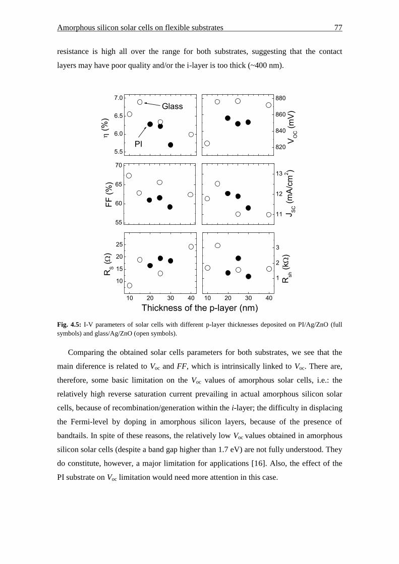
Amorphous silicon solar cells on flexible substrates 77
resistance is high all over the range for both substrates, suggesting that the contact
layers may have poor quality and/or the i-layer is too thick (~400 nm).
5.5
6.0
6.5
7.0
Glass
Rsh (
k
)J
SC (
mA
/cm
2)
VO
C (
mV
)
FF
(%
)
(
%)
PI
55
60
65
70
11
12
13
820
840
860
880
10 20 30 40
10
15
20
25
Thickness of the p-layer (nm)
RS (
)
10 20 30 40
1
2
3
Fig. 4.5: I-V parameters of solar cells with different p-layer thicknesses deposited on PI/Ag/ZnO (full
symbols) and glass/Ag/ZnO (open symbols).
Comparing the obtained solar cells parameters for both substrates, we see that the
main diference is related to Voc and FF, which is intrinsically linked to Voc. There are,
therefore, some basic limitation on the Voc values of amorphous solar cells, i.e.: the
relatively high reverse saturation current prevailing in actual amorphous silicon solar
cells, because of recombination/generation within the i-layer; the difficulty in displacing
the Fermi-level by doping in amorphous silicon layers, because of the presence of
bandtails. In spite of these reasons, the relatively low Voc values obtained in amorphous
silicon solar cells (despite a band gap higher than 1.7 eV) are not fully understood. They
do constitute, however, a major limitation for applications [16]. Also, the effect of the
PI substrate on Voc limitation would need more attention in this case.
78 Chapter 4
4.6 Laser texturing of PET substrates
The p-i-n amorphous Si thin film solar cell has a number of interfaces. The presence
of interface electronic states, particularly in the p/i interface causes open-circuit voltage
limitation [17]. In fact, using a buffer layer to passivate these interface states may help
increase Voc [18]. Since we intend to use textured substrates in order to enhance the
optical absorption, the topography of all layers will be affected by the appearence of
surface roughness, which can be more or less severe depending on the deposition
conditions [19]. The goal is to obtain optical scattering for different wavelengths of
light for the improvement of the photoresponse of the device. Looking at actual Voc
values obtained during the last two decades for amorphous silicon solar cells, one notes
that there remains in principle still a lot to be gained for Voc, as discussed in section 4.5.
So far, however, in spite of many attempts, no Voc values higher than about 1V were
obtained for a-Si:H cells, and most practically usable cells have Voc values which are
just around 0.85-0.9 V. The FF value, on the other hand is linked to Voc, and is also
reduced in cells characterized by large numbers of interface states and dangling bonds
which lead to an increase in recombination losses. One therefore cannot expect to
increase the FF value if one increases the roughness of the interfaces. However Jsc can
be increased due to the enhanced optical path length resulting from scattering in the
rough interfaces. This effect can actually overcome the lost due to the lowering of the
FF with an overall result of improving the conversion efficiency of the a-Si:H solar cell.
From the main parameters defining solar cell performance the largest margin for
further improvement lies clearly, for all types of thin film silicon solar cells, in Jsc. If
one wants, however, to keep cell thickness reasonably low, this can only be done by
optical means, i.e. by light trapping. This is a complex optical problem: it requires
suitably textured layers and very low optical absorption in all transparent layers.
In order to investigate how textures realized on plastic substrates affect the cell
efficiency, two types of samples are prepared: for use in substrate configuration (n-i-p)
solar cells, laser textured PET substrates are covered by an Al reflecting contact
deposited by thermal evaporation; and for application in superstrate configuration (p-i-
n) solar cells, textured PET substrate is coated with a transparent front contact (ZnO:Ga)
by sputtering. These samples are characterized by reflectance and transmittance
measurements as described in section 4.2.
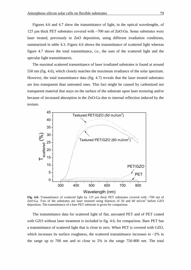
Amorphous silicon solar cells on flexible substrates 79
Figures 4.6 and 4.7 show the transmittance of light, in the optical wavelengths, of
125 μm thick PET substrates covered with ~700 nm of ZnO:Ga. Some substrates were
laser treated, previously to ZnO deposition, using different irradiation conditions,
summarized in table 4.3. Figure 4.6 shows the transmittance of scattered light whereas
figure 4.7 shows the total transmittance, i.e., the sum of the scattered light and the
specular light transmittances.
The maximal scattered transmittance of laser irradiated substrates is found at around
550 nm (fig. 4.6), which closely matches the maximum irradiance of the solar spectrum.
However, the total transmittance data (fig. 4.7) reveals that the laser treated substrates
are less transparent than untreated ones. This fact might be caused by carbonized not
transparent material that stays on the surface of the substrate upon laser texturing and/or
because of increased absorption in the ZnO:Ga due to internal reflection induced by the
texture.
300 400 500 600 700 800
0
5
10
15
20
25
30
35
40
45
PET/GZO
Textured PET/GZO (60 mJ/cm2)
Tsca
tte
red (
%)
Wavelength (nm)
Textured PET/GZO (50 mJ/cm2)
PET
Fig. 4.6: Transmittance of scattered light by 125 μm thick PET substrates covered with ~700 nm of
ZnO:Ga. Two of the substrates are laser textured using fluences of 50 and 60 mJ/cm2 before GZO
deposition. The transmittance of a bare PET substrate is given for comparison.
The transmittance data for scattered light of flat, uncoated PET and of PET coated
with GZO without laser treatment is included in fig. 4.6, for comparison. Bare PET has
a transmittance of scattered light that is close to zero. When PET is covered with GZO,
which increases its surface roughness, the scattered transmittance increases to ~2% in
the range up to 700 nm and to close to 5% in the range 750-800 nm. The total
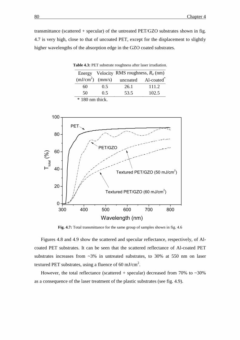
80 Chapter 4
transmittance (scattered + specular) of the untreated PET/GZO substrates shown in fig.
4.7 is very high, close to that of uncoated PET, except for the displacement to slightly
higher wavelengths of the absorption edge in the GZO coated substrates.
Table 4.3: PET substrate roughness after laser irradiation.
Energy
(mJ/cm2)
Velocity
(mm/s)
RMS roughness, Ra (nm)
uncoated Al-coated*
60 0.5 26.1 111.2
50 0.5 53.5 102.5
* 180 nm thick.
300 400 500 600 700 800
0
20
40
60
80
100
Textured PET/GZO (60 mJ/cm2)
Textured PET/GZO (50 mJ/cm2)
PET
Tto
tal (
%)
Wavelength (nm)
PET/GZO
Fig. 4.7: Total transmittance for the same group of samples shown in fig. 4.6
Figures 4.8 and 4.9 show the scattered and specular reflectance, respectively, of Al-
coated PET substrates. It can be seen that the scattered reflectance of Al-coated PET
substrates increases from ~3% in untreated substrates, to 30% at 550 nm on laser
textured PET substrates, using a fluence of 60 mJ/cm2.
However, the total reflectance (scattered + specular) decreased from 70% to ~30%
as a consequence of the laser treatment of the plastic substrates (see fig. 4.9).
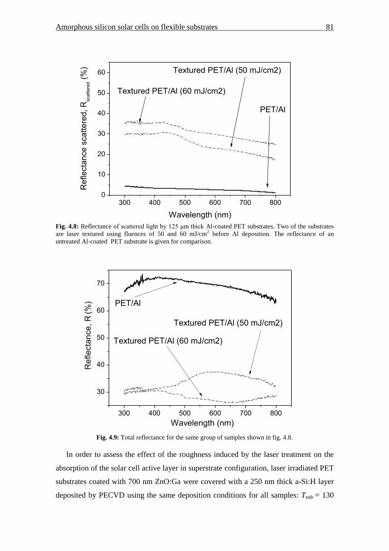
Amorphous silicon solar cells on flexible substrates 81
300 400 500 600 700 8000
10
20
30
40
50
60
Textured PET/Al (60 mJ/cm2)
Re
fle
cta
nce
sca
tte
red
, R
sca
tte
red (
%)
Wavelength (nm)
Textured PET/Al (50 mJ/cm2)
PET/Al
Fig. 4.8: Reflectance of scattered light by 125 μm thick Al-coated PET substrates. Two of the substrates
are laser textured using fluences of 50 and 60 mJ/cm2 before Al deposition. The reflectance of an
untreated Al-coated PET substrate is given for comparison.
300 400 500 600 700 800
30
40
50
60
70
PET/Al
Textured PET/Al (50 mJ/cm2)
Textured PET/Al (60 mJ/cm2)
R
efle
cta
nce
, R
(%)
Wavelength (nm)
Fig. 4.9: Total reflectance for the same group of samples shown in fig. 4.8.
In order to assess the effect of the roughness induced by the laser treatment on the
absorption of the solar cell active layer in superstrate configuration, laser irradiated PET
substrates coated with 700 nm ZnO:Ga were covered with a 250 nm thick a-Si:H layer
deposited by PECVD using the same deposition conditions for all samples: Tsub = 130
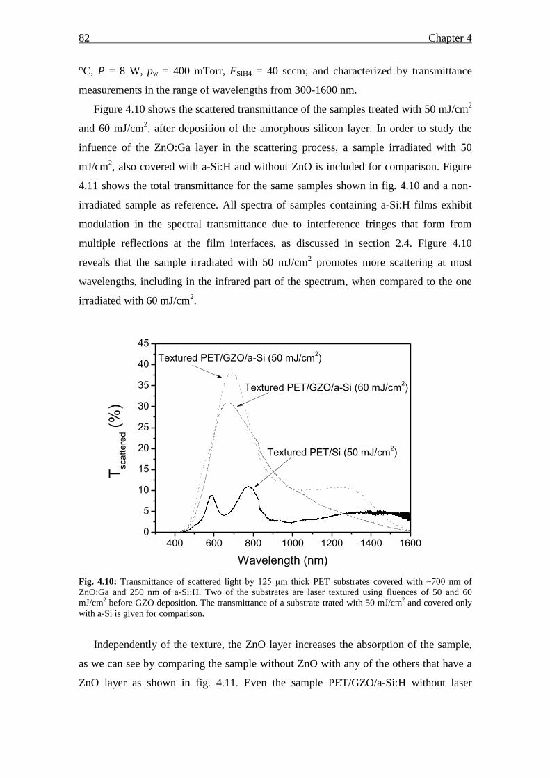
82 Chapter 4
°C, P = 8 W, pw = 400 mTorr, FSiH4 = 40 sccm; and characterized by transmittance
measurements in the range of wavelengths from 300-1600 nm.
Figure 4.10 shows the scattered transmittance of the samples treated with 50 mJ/cm2
and 60 mJ/cm2, after deposition of the amorphous silicon layer. In order to study the
infuence of the ZnO:Ga layer in the scattering process, a sample irradiated with 50
mJ/cm2, also covered with a-Si:H and without ZnO is included for comparison. Figure
4.11 shows the total transmittance for the same samples shown in fig. 4.10 and a non-
irradiated sample as reference. All spectra of samples containing a-Si:H films exhibit
modulation in the spectral transmittance due to interference fringes that form from
multiple reflections at the film interfaces, as discussed in section 2.4. Figure 4.10
reveals that the sample irradiated with 50 mJ/cm2 promotes more scattering at most
wavelengths, including in the infrared part of the spectrum, when compared to the one
irradiated with 60 mJ/cm2.
400 600 800 1000 1200 1400 16000
5
10
15
20
25
30
35
40
45
Textured PET/Si (50 mJ/cm2)
Textured PET/GZO/a-Si (60 mJ/cm2)
Textured PET/GZO/a-Si (50 mJ/cm2)
Tsca
tte
red (
%)
Wavelength (nm)
Fig. 4.10: Transmittance of scattered light by 125 μm thick PET substrates covered with ~700 nm of
ZnO:Ga and 250 nm of a-Si:H. Two of the substrates are laser textured using fluences of 50 and 60
mJ/cm2 before GZO deposition. The transmittance of a substrate trated with 50 mJ/cm
2 and covered only
with a-Si is given for comparison.
Independently of the texture, the ZnO layer increases the absorption of the sample,
as we can see by comparing the sample without ZnO with any of the others that have a
ZnO layer as shown in fig. 4.11. Even the sample PET/GZO/a-Si:H without laser
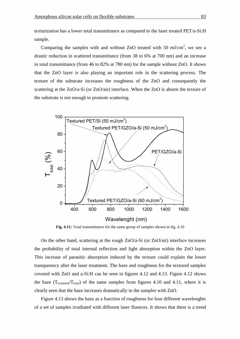
Amorphous silicon solar cells on flexible substrates 83
texturization has a lower total transmittance as compared to the laser treated PET/a-Si:H
sample.
Comparing the samples with and without ZnO treated with 50 mJ/cm2, we see a
drastic reduction in scattered transmittance (from 38 to 6% at 700 nm) and an increase
in total transmittance (from 46 to 82% at 780 nm) for the sample without ZnO. It shows
that the ZnO layer is also playing an important role in the scattering process. The
texture of the substrate increases the roughness of the ZnO and consequently the
scattering at the ZnO/a-Si (or ZnO/air) interface. When the ZnO is absent the texture of
the substrate is not enough to promote scattering.
400 600 800 1000 1200 1400 1600
0
20
40
60
80
100
PET/GZO/a-Si
Wavelenght (nm)
Tto
tal (
%)
Textured PET/GZO/a-Si (60 mJ/cm2)
Textured PET/GZO/a-Si (50 mJ/cm2)
Textured PET/Si (50 mJ/cm2)
Fig. 4.11: Total transmittance for the same group of samples shown in fig. 4.10
On the other hand, scattering at the rough ZnO/a-Si (or ZnO/air) interface increases
the probability of total internal reflection and light absorption within the ZnO layer.
This increase of parasitic absorption induced by the texture could explain the lower
transparency after the laser treatment. The haze and roughness for the textured samples
covered with ZnO and a-Si:H can be seen in figures 4.12 and 4.13. Figure 4.12 shows
the haze (Tscattered/Ttotal) of the same samples from figures 4.10 and 4.11, where it is
clearly seen that the haze increases dramatically in the samples with ZnO.
Figure 4.13 shows the haze as a function of roughness for four different wavelenghts
of a set of samples irradiated with different laser fluences. It shows that there is a trend
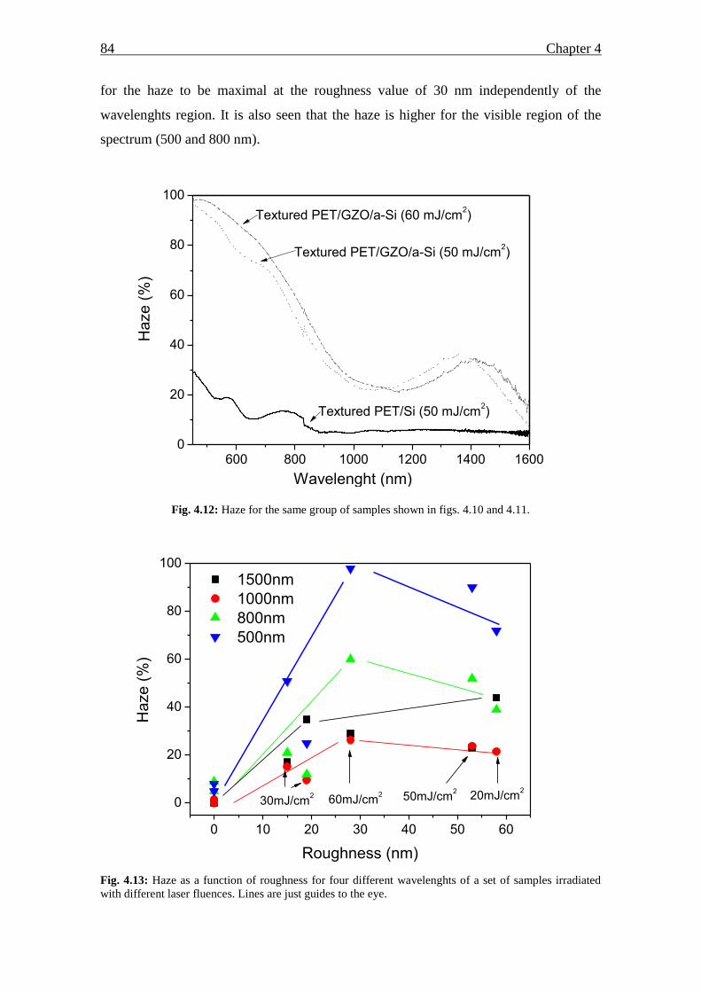
84 Chapter 4
for the haze to be maximal at the roughness value of 30 nm independently of the
wavelenghts region. It is also seen that the haze is higher for the visible region of the
spectrum (500 and 800 nm).
600 800 1000 1200 1400 16000
20
40
60
80
100
Wavelenght (nm)
Ha
ze
(%
)
Textured PET/GZO/a-Si (50 mJ/cm2)
Textured PET/GZO/a-Si (60 mJ/cm2)
Textured PET/Si (50 mJ/cm2)
Fig. 4.12: Haze for the same group of samples shown in figs. 4.10 and 4.11.
0 10 20 30 40 50 60
0
20
40
60
80
100
20mJ/cm2
50mJ/cm2
60mJ/cm2
1500nm
1000nm
800nm
500nm
Ha
ze
(%
)
Roughness (nm)
30mJ/cm2
Fig. 4.13: Haze as a function of roughness for four different wavelenghts of a set of samples irradiated
with different laser fluences. Lines are just guides to the eye.
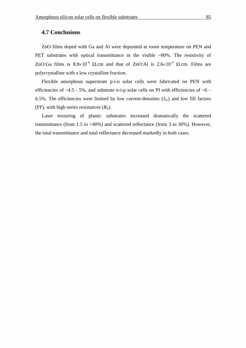
Amorphous silicon solar cells on flexible substrates 85
4.7 Conclusions
ZnO films doped with Ga and Al were deposited at room temperature on PEN and
PET substrates with optical transmittance in the visible ~80%. The resistivity of
ZnO:Ga films is 8.810-4
Ω.cm and that of ZnO:Al is 2.610-3
Ω.cm. Films are
polycrystalline with a low crystalline fraction.
Flexible amorphous superstrate p-i-n solar cells were fabricated on PEN with
efficiencies of ~4.5 - 5%, and substrate n-i-p solar cells on PI with efficiencies of ~6 –
6.5%. The efficiencies were limited by low current-densities (Jsc) and low fill factors
(FF), with high series resistances (RS).
Laser texturing of plastic substrates increased dramatically the scattered
transmittance (from 1.5 to >40%) and scattered reflectance (from 3 to 30%). However,
the total transmittance and total reflectance decreased markedly in both cases.

86 Chapter 4
References
[1] J. Escarre et al, Solar Energy Materials and Solar Cells, 87 (2005) p. 333.
[2] C. Bundesmann et al., Appl. Phys. Lett. 83 (10) (2003) p. 1974.
[3] J.M. Calleja, M. Cardona, Phys. Rev. B, 16 (1977) p. 3753.
[4] G.Heiland et al., Solid State Physics, ed. F.Seitz and D.Turnbull, Academic, New York,
8 (1959) p. 191.
[5] S.K. Sharma and G.J. Exarhos, Solid State Phenom. 55 (1997) p. 32.
[6] M. Snure, A.Tiwari, J. Appl. Phys. 104 (2008) p. 73707.
[7] A. Banerjee, S. Guha, Journal of Applied Physics, 69 (1991) p. 1030.
[8] T. S derstr m, F.-J. Haug, X. Niquille, C. Ballif, Progress in Photovoltaics: Research
and Applications, 17 (2009) p. 165.
[9] J. Bailat, V. Terrazzoni-Daudrix, J. Guillet, F. Freitas, X. Niquille, A. Shah, C. Ballif, T.
Scharf, R.Morf, A. Hansen, D. Fischer, Y. Ziegler, A. Closset, In Proceedings of 20th
European PVSEC (2005) p. 1529.
[10] J. Yang, A. Banerjee, S. Guha, Applied Physics Letters, 70 (1997) p. 2975.
[11] K. Saito, M. Sano, H. Otoshi, A. Sakai, S. Okabe, K. Ogawa, In Proceedings of 3rd
World PVSEC, Osaka, Japan (2003) p. 2793.
[12] M. Tanda, K. Tabuchi, M. Uno, S. Kato, Y. Takeda, S. Iwasaki, Y. Yokohama, T. Wada,
M. Shimosawa, Y. Sakakibara, A. Takano, H. Nishihara, H. Enomoto, T. Kamoshita, In
Proceedings of 31st IEEE PVSC, Lake Buona Vista, USA (2005) p. 1560.
[13] F.-J. Haug, T. Söderström, M. Python, V. Terrazzoni-Daudrix, X. Niquille, C. Ballif,
Solar Energy Materials and Solar Cells, 93 (2009) p. 884.
[14] P. Alpuim, G.M. Junior, S.A. Filonovich, P. Roca i Cabarrocas, J.-E. Bouree, E.V.
Johnson, Y.M. Soro, In Proceedings of 23rd
European PVSEC (2008) p. 2455.
[15] K. Tao, D. Zhang, L. Wang, J. Zhao, H. Cai, Y. Sui, Z. Qiao, Q. He, Y. Zhang, Y. Sun,
Solar Energy Materials and Solar Cells, 94 (2010) p. 709.
[16] A. Shah, ed., Thin-film Silicon Solar Cells, First edition, EPFL Press (2010).
[17] L. Jiang, J.H. Lyou, S. Rane, E.A. Schiff, Q. Wang, and Q. Yuon, In Proceedings of
Materials Research Society Symposium, 609 (2000).
[18] Q.Wang, E. Iwaniczko, Y. Xu, W. Gao, B.P. Nelson, A.H. Mahan, R.S. Crandall, and
H.M. Branz, In Proceedings of Materials Research Society Symposium, 609 (2000).
[19] M. Zeman, R.A.C.M.M. Van Swaaij, M. Zuiddam, J.W. Metselaar, and R.E.I. Schropp,
In Proceedings of Materials Research Society Symposium, 557 (1999) p. 725.
Chapter 5
5 Microcrystalline silicon solar cells on flexible PI substrate
In thin film silicon solar cells on opaque substrates in n-i-p deposition sequence
where the textured TCO (transparent conductive oxide) layer serves as a back reflector,
one can independently optimize the morphology of the TCO layer without compromise
on transparency and conductivity of this layer and further adjust the electro-optical
properties of the back contact by using additional layers on top of the textured TCO. In
the present work, we use this strategy to obtain textured back reflectors for solar cells in
n-i-p deposition sequence on non-transparent flexible plastic foils. Gallium doped ZnO
(ZnO:Ga) films were deposited on polyimide substrates by DC magnetron sputtering at
a temperature of 200ºC. A wet-chemical etching step was performed by dipping the
ZnO:Ga covered foil into a diluted HCl solution. The textured ZnO:Ga is then coated
with a highly reflective Ag/ZnO double layer. On this back reflector we develop thin
film silicon solar cells with a microcrystalline silicon absorber layer. The current
density for the cell with the textured ZnO:Ga layer is ~23 mA/cm², 4 mA/cm² higher
than the one without such layer, and a maximum efficiency of 7.5% is obtained for a
1cm² cell.

88 Chapter 5
5.1 Introduction
For high efficiency of amorphous (a-Si:H) and microcrystalline (µc-Si:H) thin film
silicon solar cells, light trapping of the incident light within the silicon absorber layers
becomes crucial in order to further reduce the cell thickness, which leads to reduction of
the light-induced degradation effects for a-Si:H material [10] and more effective cycle
times in production for both a-Si:H and µc-Si:H solar cells [2]. Light scattering at the
interfaces is usually achieved by texturing the front TCO electrodes and/or the back
reflectors [11–14]. Some TCO materials already have a suitable texture in the as-
deposited state. On plastic foils, ZnO textured in the as-deposited state obtained by LP-
CVD or 2D periodic structures have been used to provide light trapping in the active
layers of n-i-p devices [2,7]. Sputter-deposited ZnO can be textured by a post-
deposition wet-chemical etching step [15,16]. For the n-i-p deposition sequence in
substrate configuration where the textured TCO serves as a back reflector, this approach
has the advantage of using an optimized morphology of the TCO layer, where the
electro-optical properties can be adjusted by using additional layers on top of the
textured TCO. This technique has been used successfully for solar cells in both p-i-n
and n-i-p deposition sequence on transparent glass substrates [11,17]. In the present
work, we use this strategy to obtain textured back reflectors for n-i-p solar cells on
flexible polyimide foil.
5.2 Experimental details
Microcrystalline thin film silicon solar cells are prepared on 10×10 cm² and 125 µm
thick PI foils. The substrates for smooth cells are covered with a thermally evaporated
700 nm Ag layer and an 80 nm sputtered ZnO:Ga, both deposited at room temperature.
In order to obtain rough cells, an 800 nm ZnO:Ga layer is deposited directly on PI by
DC magnetron sputtering at a substrate temperature of 200 ºC. This layer is textured by
a post-deposition wet-chemical etching in a 0.5% diluted HCl solution for 30 seconds.
The back contact is finalized with an additional highly reflecting Ag/ZnO double layer
that conformally covers the textured ZnO:Ga surface.
The thin film silicon layers are deposited in n-i-p sequence by plasma enhanced
chemical vapor deposition (PECVD) using very high frequency excitation (81.36 MHz).
Microcrystalline silicon solar cells on flexible PI substrate 89
The substrate temperature is 200 ºC for intrinsic and doped layers. The power density
and chamber pressure for deposition of intrinsic layers are 210 mW/cm2 and 7.5×10
-1
Torr, respectively. Doped layers are deposited at power densities and pressures of 470
mW/cm2 and 2.3 Torr for n-layers, and 140 mW/cm
2 and 7.5×10
-1 Torr for p-layers.
The hydrogen dilution or silane/hydrogen gas mixture is, alternatively, defined in this
chapter as silane concentration SC, i.e. the ratio between the silane gas flow to the
process chamber and the total gas flow (SC = [SiH4] / ([SiH4]+[H2]). A low SC is
equivalent to a high hydrogen dilution. For the intrinsic layers, SC is varied between 5%
and 7%.
The front transparent contacts made of 70 nm thick ITO layers are prepared
by radio-frequency (RF) magnetron sputtering at room temperature using a In2O3:SnO2
target (95/5 wt.%) in an argon/oxygen atmosphere with relative oxygen content, defined
as [O2] / [O2+Ar], of 0.1%.
The individual solar cells with an area of 1×1 cm2 are defined by using a shadow
mask during ITO deposition on the 10×10 cm² substrate. Front metal finger electrodes
are prepared by silver evaporation. Finally, standard annealing procedure of finished
solar cells is performed in air at 160°C for 30 minutes. The complete device layer
sequences are for smooth cells: PI/Ag/ZnO:Ga/n-i-p/ITO and for rough cells:
PI/textured ZnO:Ga/Ag/ZnO:Al/n-i-p/ITO. Figure 5.1 shows schematics of the solar
cells on PI on smooth (fig. 5.1a) and rough (fig. 5.1b) back reflectors.
For comparison solar cells are also deposited on glass substrates with the same layer
sequences.
The solar cell parameters open circuit voltage (Voc), fill factor (FF) and short circuit
current density (Jsc) are determined from current-voltage (I-V) measurements under
simulated AM1.5G illumination at 25 ºC. The external quantum efficiency (EQE) is
obtained from spectral response measurements in the range of 300-1100 nm. The
integrated current from the EQE curves under short circuit conditions is used to
calculate the conversion efficiency in order to avoid possible effects from current
collection around the 1cm² solar cells or from imprecision in determination of the cell
area.
Raman spectroscopy is used to evaluate the crystalline volume fraction of the
intrinsic layers in the solar cells. Raman measurements are performed directly on the
solar cells using a frequency-doubled Nd:YAG laser with excitation wavelength of 532
nm.
90 Chapter 5
(a) (b)
Fig. 5.1: Structures of the solar cells on PI without (a) and with (b) textured ZnO:Ga layer.
5.3 n-i-p solar cells on smooth PI substrate
Figure 5.2 shows the performance parameters of solar cells deposited on the smooth
PI/Ag(700 nm)/ZnO(80 nm) substrate as a function of silane concentration (SC) of the
i-layer. For reference and in order to assess the effect of the substrate on the
performance of the solar cells, we prepared identical cells on smooth glass covered with
a standard Ag/ZnO back reflector, optimized for glass substrate. We observed a similar
trend of the performance parameters for the cells on PI when compared to the ones on
glass. However, the Voc was around 20-40 mV lower for the cells on PI. A reason for the
lower Voc could be the higher i-layer crystallinity of the cells deposited on PI as
measured by Raman spectroscopy on the solar cells. This is shown in fig. 5.3. Why the
PI substrate possibly promotes the growth of films with higher crystalline volume
fraction is not clear at the moment. Despite of the apparent higher crystallinity in the i-
layer of the solar cells prepared on PI with respect to the ones prepared on glass, the Jsc
is lower for cells deposited at SC below 6% where one would instead expect higher
carrier mobility and carrier collection at higher crystallinity. We speculate that this
results from absorption losses in the Ag/ZnO back contact [11], which is not optimized
for the PI substrate foil. The cell deposited with SC of 6.1% showed the highest Voc
Microcrystalline silicon solar cells on flexible PI substrate 91
(505 mV) and FF of 70.7%. For this reason we chose the deposition conditions of this
cell for further optimization of the solar cells on PI with rough TCO.
2
4
6
8
Silane concentration SC [%]
JS
C [
mA
/cm
2]
VO
C [
mV
]
FF
[%
]
[
%]
5 6 740
50
60
70
5 6 7
9
12
15
18
21
PI
Glass
480
500
520
540
560
Fig. 5.2: I-V parameters of solar cells with different i-layer silane concentrations deposited on PI/Ag/ZnO
(full symbols) and glass/Ag/ZnO (open symbols).
Fig. 5.3: Raman crystallinity as a function of the i-layer silane concentration of solar cells deposited on PI
(full symbols) and glass (open symbols). Lines are guides to the eye.
5.0 5.5 6.0 6.5 7.0
0
20
40
60
80
Ra
ma
n c
rysta
llin
ity
C
RS [
%]
Silane concentration SC [%]
PI
Glass
92 Chapter 5
Figure 5.4 shows the I-V curve of the solar cell on smooth PI and on glass substrate
with an i-layer thickness of 1.8 µm deposited at SC = 6.1%, which yields a current
density of 18.9 mA/cm2 on PI and 20.7 mA/cm
2 on glass.
-0.1 0.0 0.1 0.2 0.3 0.4 0.5
-20
-15
-10
-5
0
5
Cu
rre
nt
de
nsity J
SC [
mA
/cm
2]
Voltage V [V]
PI Glass
Voc 505 521
Isc 18.9 20.7
FF 70.7 72.7
eff 6.8 7.9PI
Glass
Fig. 5.4: Comparison of the I-V curves of solar cells on PI/Ag/ZnO (plain curve) and glass/Ag/ZnO
(dashed curve).
5.4 n-i-p solar cells on PI with textured ZnO:Ga
To further enhance the current of cells on PI, ZnO:Ga layers were developed for
application as textured back reflector [18]. This development was first carried out on
glass and later transferred to application on the PI substrate1.
Figure 5.5 shows the EQE of a solar cell prepared on ZnO:Ga deposited on PI,
textured by post-deposition wet-chemical etching in HCl solution for 30 seconds, and
covered with a highly reflecting Ag/ZnO double layer. For comparison the EQE of the
cell on flat PI is shown. We observe a strong increase in EQE especially above 600 nm
for the cell with the textured ZnO:Ga layer accompanied by efficient reduction of
interference fringes. The cell on structured TCO delivers a current density of ~23
mA/cm2, more than 4 mA/cm
2 higher than the one on flat PI, and an efficiency of 7.5%
1 These layers were developed on the scope of another PhD thesis and more details can be found in
reference [18]. It was not possible to obtain the values of thickness and roughness of the ZnO:Ga layers
on PI, because of the experimental challenges of performing these kind of measurements on flexible
substrates.
Microcrystalline silicon solar cells on flexible PI substrate 93
is achieved for a 1 cm² cell. However, the FF decreased from 70.7% to 68%, and the Voc
was 30 mV lower. These reductions in FF and Voc are expected and related to the
roughness of the substrate [19]. The improvement in current was observed essentially
for wavelengths above 650 nm, corresponding to the light trapping region for
microcrystalline solar cells [11].
400 600 800 10000.0
0.2
0.4
0.6
0.8
1.0
18.9 mA/cm2
EQ
E
Wavelength [nm]
23.1 mA/cm2
Fig. 5.5: Comparison of EQE’s of solar cells on PI/Ag/ZnO (dashed line) and PI/textured
ZnO:Ga/Ag/ZnO (full line).
Figure 5.6 shows the corresponding IV curve of this cell and, for comparison, the
curve of an identical cell deposited on a standard textured TCO/Ag/ZnO back reflector
on glass. One can clearly see the pronounced difference in Voc, with lower value for the
cell on PI, as discussed in section 5.3.
Table 5.1: I-V parameters of solar cells under AM1.5 illumination.
Substrate type Voc (mV) JSC (mA/cm
2) FF (%) η (%)
Smooth glass 521 20.7 72.7 7.9
Smooth PI 505 18.9 70.7 6.8
Glass+rough TCO 525 22.8 71 8.5
PI+rough ZnO:Ga 475 23.1 68 7.5
Results presented above and summarized in table 5.1 showed that the well-
established technology of post-deposition texturing of TCO films as scattering layers to
94 Chapter 5
promote light trapping in thin film silicon solar cells can be successfully transferred to
application with flexible plastic substrates.
-0.1 0.0 0.1 0.2 0.3 0.4 0.5
-20
-15
-10
-5
0
5
PI
Cu
rre
nt
de
nsity J
SC [
mA
/cm
2]
Voltage V [V]
PI+rough ZnO:Ga Glass+rough TCO
Voc 475 525
Isc 23.1 22.8
FF 68 71
eff 7.5 8.5
Glass
Fig. 5.6: Comparison of the I-V curves of solar cells on PI/textured ZnO:Ga /Ag/ZnO (plain curve) and
glass/textured TCO/Ag/ZnO (dashed curve).
5.5 Conclusions
We have presented our development of microcrystalline single-junction n-i-p thin
film silicon solar cells on flexible polyimide substrate. The results of solar cells on
smooth PI showed similar behavior in terms of performance parameters in comparison
to cells deposited on smooth glass. The Voc was around 20-40 mV lower for the cells on
PI, which is related to higher i-layer crystallinity of cells on PI. We developed a
textured ZnO:Ga layer to promote light trapping in the solar cells on PI that yield more
than 23 mA/cm2 on absorbers of 1.8 µm thickness with cell efficiencies of up to 7.5%.
Microcrystalline silicon solar cells on flexible PI substrate 95
References
[1] A. Banerjee, S. Guha, Journal of Applied Physics, 69 (1991) p. 1030.
[2] T. S derstr m, F.-J. Haug, X. Niquille, C. Ballif, Progress in Photovoltaics: Research
and Applications, 17 (2009) p. 165.
[3] J. Bailat, V. Terrazzoni-Daudrix, J. Guillet, F. Freitas, X. Niquille, A. Shah, C. Ballif, T.
Scharf, R.Morf, A. Hansen, D. Fischer, Y. Ziegler, A. Closset, In Proceedings of 20th
European PVSEC (2005), p. 1529.
[4] J. Yang, A. Banerjee, S. Guha, Applied Physics Letters, 70 (1997) p. 2975.
[5] K. Saito, M. Sano, H. Otoshi, A. Sakai, S. Okabe, K. Ogawa, In Proceedings of 3rd
World PVSEC, Osaka, Japan (2003) p. 2793.
[6] M. Tanda, K. Tabuchi, M. Uno, S. Kato, Y. Takeda, S. Iwasaki, Y. Yokohama, T. Wada,
M. Shimosawa, Y. Sakakibara, A. Takano, H. Nishihara, H. Enomoto, T. Kamoshita, In
Proceedings of 31st IEEE PVSC, Lake Buona Vista, USA (2005) p. 1560.
[7] F.-J. Haug, T. Söderström, M. Python, V. Terrazzoni-Daudrix, X. Niquille, C. Ballif,
Solar Energy Materials and Solar Cells, 93 (2009) p. 884.
[8] P. Alpuim, G.M. Junior, S.A. Filonovich, P. Roca i Cabarrocas, J.-E. Bouree, E.V.
Johnson, Y.M. Soro, In Proceedings of 23rd
European PVSEC (2008) p. 2455.
[9] K. Tao, D. Zhang, L. Wang, J. Zhao, H. Cai, Y. Sui, Z. Qiao, Q. He, Y. Zhang, Y. Sun,
Solar Energy Materials and Solar Cells, 94 (2010) p. 709.
[10] D.L. Staebler, C.R. Wronski, Applied Physics Letters, 31 (1977) p. 292.
[11] J. Müller, B. Rech, J. Springer, M. Vanecek, Solar Energy, 77 (2004) p. 917.
[12] S. Faÿ, L. Feitknecht, R. Schlüchter, U. Kroll, E. Vallat-Sauvain, A. Shah, Solar Energy
Materials and Solar Cells, 90 (2006) p. 2960.
[13] J. Hüpkes, B. Rech, O. Kluth, T. Repmann, B. Zwaygardt, J. Müller, R. Drese, M.
Wuttig, Solar Energy Materials and Solar Cells, 90 (2006) p. 3054.
[14] T. Tohsophon, J. Hüpkes, H. Siekmann, B. Rech, M. Schultheis, N. Sirikulrat, Thin
Solid Films, 516 (2008) p. 4628.
[15] O. Kluth, B. Rech, L. Houben, S. Wieder, G. Schöpe, C. Beneking, H. Wagner, A. Löffl,
H.. Schock, Thin Solid Films, 351 (1999) p. 247.
[16] W. Böttler, V. Smirnov, J. Hüpkes, F. Finger, Journal of Non-Crystalline Solids (2012)
doi:10.1016/j.jnoncrysol.2011.12.100.
[17] W. Böttler, V. Smirnov, A. Lambertz, J. Hüpkes, F. Finger, Phys. Status Solidi C, 7
(2010) p. 1069.
[18] M. Warzecha, PhD Thesis, Forschungszentrum Jülich, Germany (2012).
[19] T. Söderström, F.-J. Haug, V. Terrazzoni-Daudrix, C. Ballif, Journal of Applied Physics,
103 (2008) p. 114509.

96 Chapter 5
Chapter 6
6 Shape sensors based on piezoresistive doped µc-Si:H
This chapter describes the manufacture of a thin skin-like piezo-resistor strain-
sensing membrane and the miniaturization of piezoresistive sensor arrays based on n-
type hydrogenated microcrystalline silicon thin films (µc-Si:H) deposited on flexible
polyimide substrates (PI). The µc-Si:H thin films, prepared by hot-wire chemical vapor
deposition, have a piezoresistive gauge factor (GF) of -32.2.
Six of the sensors batch processed on the 15 μm-thick membrane were cut and used
in a test structure to track the simulated movement of the head of a bedridden patient.
The sensors were glued to both sides of a 3 mm-thick acrylic rectangular plate, to
collect strain data from the tensile and compressive surfaces of the plate upon bending.
The sensor output electrical signal was obtained by inserting the sensors into
Wheatstone bridge circuits and recording the output voltage of the bridge as a function
of the sensor/plate deformation. The results using quarter-, half- and full-bridge
configurations were compared.
In order to give a further step toward a shape sensitive electronic textile, nine sensors
were glued and interconnected using a machine sewed conductive thread and
preliminary tests on their output response under random loading conditions were
performed.
Test structures, consisting of microresistors having lateral dimensions in the range
from 50 to 100 m and thickness of 120 nm were defined in an array by reactive ion
etching. Metallic pads, forming ohmic contacts to the sensing elements, were defined
by a lift-off process.
98 Chapter 6
6.1 Introduction
The piezoresistive property of crystalline silicon has long been known to scientists
and engineers [1] and most strain gauge sensors use that property as their operation
principle [2]. More recently, the piezoresistive effect has also been found in doped
hydrogenated microcrystalline silicon thin films (µc-Si:H) [3,4]. In particular, the
combination of the mechanical properties of plastic substrates with the electrical
properties of doped µc-Si:H deposited at 100-150ºC opened a way to design new types
of piezoresistive sensors [3,6].
The piezoresistive property of doped µc-Si:H deposited at low substrate temperature
(150ºC) on flexible polyimide (PI) and polyethylene naphthalate (PEN) substrates by
hot-wire chemical vapor deposition (HWCVD) was investigated in previous studies
[3,5] and the results showed that GF is positive for p-type films and is negative for n-
type films. It is consistent with the idea that because the films are semi-crystalline and
isotropic, at least within planes parallel to the substrate, they retain the sign of the
largest (in absolute value) piezoresistive coefficient of c-Si which is π44=138×10−11
Pa−1
for p-type and π11=−102×10−11
Pa−1
for n-type material. π11 denotes the fractional
change in resistivity for a stress parallel to the current flow, while π44 denotes the
fractional change in resistivity for a shear stress (perpendicular to the current flow).
These studies are now extended to flexible piezoresistive sensor fabrication by
manufacture of a thin “skin-like” piezo-resistor sensing membrane followed by cutting
and transfer to other surfaces. Strain sensors fabricated using the first of these
approaches are characterized in the static and quasi-static actuation modes and are
reported here. A large sensor in the shape of a strip is used to monitor the movements of
a plastic plate that simulates the movements of the head of a bedridden patient.
Piezoresistive sensors are embedded in a textile fabric in order to obtain a shape
sensitive electronic textile to be tested in a clinical environment with the aim to perceive
levels of discomfort in patients that have lost the ability to change their posture by
analysing the movements of the body that healthy people usually do under similar
conditions.
Shape sensors based on piezoresistive doped µc-Si:H 99
6.2 Experimental details
6.2.1 Film preparation
Films are deposited in a load-locked high-vacuum system composed of twin
chambers for HWCVD and rf-PECVD. N-type µc-Si:H films are deposited by HWCVD
from gaseous mixtures of silane (Fsilane = 1.86 sccm), hydrogen (FH2 = 33.9 sccm) and
phosphine – 98% diluted in hydrogen (FPH3/H = 1.862 sccm) resulting in a 95%
hydrogen diluted reactive gas mixture. A working pressure of 40 mTorr is used. The
substrate holder is placed 7 cm above a single S-shaped tantalum filament, 0.5 mm thick
and 14 cm long. The filament is resistively heated (Tfil ~ 1750 °C) for deposition, using
a DC power supply (Ifil = 14 A) that pyrolytically decomposes the reactant gases at the
filament surface. Substrates are polyimide foils (PI) with area 33×33 mm2. Substrate
temperature is 150 ºC for all depositions.
6.2.2 Sensor fabrication
Large-area sensors are fabricated by deposition through 0.4 mm-thick stainless steel
masks on a 15 μm-thick PI membrane. The first mask is used for definition of the
piezoresistive element island (3×3 mm2). In the next step, Al is thermally evaporated
through a second mask that defines the parallel contacts overlapping the island, the 200
μm-wide interconnects, and the pads. Piezoresistor dimensions are set by the gap
between the parallel contacts (1 mm), the width of the island (3 mm) and the thickness
of the films (~100 nm). The squared plastic substrates are then cut into individual
sensors. Each sensor sits on a piece of 15 μm-thick PI with area ~ 5 5 mm2.
6.2.3 Piezoresistive response characterization
Piezoresistive gauge factor, GF, is measured by four-point bending tests, where each
sensor is glued to a larger piece of 125 μm thick polyimide that is inserted in a
Shimadzu-AG-IS 500 N Testing Instrument with characteristic lengths 10-30 mm
(distance between the inner and the outer points of application of the force). Control
software is Trapezium2 from Shimadzu Corp. Four other sensors are glued onto an
acrylic plate, with dimensions 250 mm 90 mm 3 mm, two of them attached to the
upper surface of the plate and another two to the bottom surface. The bendable acrylic
100 Chapter 6
plate is used to simulate the surface of a supporting cushion of a virtual bedridden
patient, with the width of a human head (250 mm). The movement of the human head is
represented by the up-and-down displacement of the inner bars of the 4-point
instrument, and its contact area with the cushion is the 10 mm region between the inner
points. For each piezoresistor, the relative resistance change, 0R
R, where R0 is the
undeformed resistance of the sensor and ΔR is the change in resistance upon bending, is
related to the applied strain, ε, by the equation 0R
R= GFε. In four-point bending
experiments, the shape of the bended specimen can be calculated from the theory of
pure bending of a plate to a cylindrical surface, valid between the inner loading points
[7]. In this region, the radius of curvature, r, is constant and given by:
z
aalr
6
43 2 (1)
where z is the displacement of the inner loading bars, a is the distance between the outer
and inner loading bars and l is the distance between outer bars in the four-point bending
system (see fig. 6.1).
Fig. 6.1: Schematic diagram of the 4-point bending instrument (Shimadzu-AG-IS 500 N) and contacts
used to characterize the piezoresistive response of the sensors. The outer and inner loading bars are
represented by green circles and the contacts by gray rectangles and lines in lower part of figure.
Shape sensors based on piezoresistive doped µc-Si:H 101
Assuming that the neutral plane of the sensor (substrate + film) is symmetrically
placed between the two free surfaces of the substrate and no slip occurs at the film-
substrate interface, the strain in the film in the longitudinal direction is:
243
3
aal
dz
(2)
where d is the substrate thickness.
For the first set of experiments (measurement of the GF of the sensors) a = 10 mm
and l = 3a and thus eq. (2) yields, upon substitution:
25
3
a
dz (3)
For the second set of experiments (simulation of the movement of a bedridden
patient), a = 10 mm and l = 10.5a and thus, upon substitution in eq. (2), one obtains:
25.27
3
a
dz (4)
The signal of the sensors is the output voltage of a Wheatstone bridge circuit in
which the sensors are inserted in the quarter-, half- or full-bridge configuration (see
table 6.1). A NI-USB 6210 data acquisition module connected to a PC laptop completed
the setup. In some experiences the resistance of the sensors is directly monitorized by
connecting the sensor pads to a digital multimeter that communicated with the PC
laptop through a GPIB connection.
The sensitivity of the Wheatstone bridge circuit can be expressed in terms of the
change in bridge output voltage due to a small change in the resistance of one of the
bridge arms, generally the unknown resistance arm, i.e. ΔRx. A general expression for
the change in output voltage of the bridge, ΔVout, with respect to a small change in Rx is:
( ) (5)
where Vin is the input voltage, and R and Rx are the known and unknown resistances of
one bridge arm, respectively.
102 Chapter 6
The maximum sensisitivity is achieved when the resistors in the bridge have the
same resistance. Hence by letting R = Rx in eq. (5) we get an alternate expression for the
bridge sensitivity:
(6)
One of the problems of strain measurement is thermal effect. Besides external force,
changing temperatures elongate or contract the measuring object with a certain linear
expansion coefficient. Accordingly, a strain gauge bonded to the object bears thermally-
induced apparent strain. Other interference effects can affect the strain measurement,
e.g. humidity, hydrostatic pressure, magnetic fields, radiation, etc. Some of these
effects can be compensated by the appropriate use of the Wheatstone bridge circuit. If,
for example, the temperature variation occurs during the mechanical loading of the
structural part, the strain signal will be a composite with one component of the desired
effect from the mechanical stress, εM, and with other component of the undesired effect
from the thermal expansion, εW:
( ) (7)
If four strain gauges are applied to the specimen and connected into a full bridge as
shown in table 6.1, we have:
[( ) ( ) ( ) ( ) ]
(8)
We can see that the thermal component in the total strain, εW, has the same sign for
all strain gauges, provided they are all subjected to the same change in temperature. The
interference effect, εW, has been compensated. The same method of compensation can
be used for a half bridge, but cannot be implemented with the quarter bridge. The only
way to overcome this is to use a “compensating strain gauge” to expand the quarter
bridge into a half bridge. It is very important to select and apply the compensating strain
gauge correctly in order to achieve the correct result. The compensating strain gauge
must have the same physical properties as the “active” strain gauge; be applied in a spot
where it will be subjected to the same interference effect as the active strain gauge; and
Shape sensors based on piezoresistive doped µc-Si:H 103
only be subjected to the interference effect and never to the quantity to measured or its
side effects.
Table 6.1: Number and position of sensors, output voltage and circuit diagram for several bridge
configurations used in this work.
Configuration Number of
sensors
Circuit Output voltage,
Vout
Vout
(measured
@z=10 mm)
Full bridge 2 (ε<0)
+
2 (ε>0)
150 mV
Half bridge 1 (ε<0)
+
1 (ε>0)
inout VGF
V2
89 mV
Quarter bridge 1 (ε<0)
or
1 (ε>0)
44 mV
6.3 skin-like piezoresistive sensing membranes
Figure 6.2 shows on the right axis the resistance of a “skin-like” sensing membrane
as a function of time, during a four-point bending experiment consisting of 5 loading
cycles. The membrane is glued to the tensile surface of a 33 mm 10 mm piece of 125
μm-thick polyimide with appropriate size and enough rigidity to be inserted in the 4-
point bending set up.
The left axis shows the displacement of the inner loading bars, z. It can be seen that
the resistance instantaneously adjusts to the displacement while the graphs are half a
period out of phase. This is due to the negative gauge factor of the n-type sensor placed
Vout
R
R
R
R1
Vin
Vout
R
R2 R1
Vin
R
R4
Vout
R3
R1
Vin
R2 inout VGFV
inout VGF
V4
104 Chapter 6
on the tensile surface. When the sensor is placed on the compressive surface, the two
graphs are in phase.
Fig. 6.2: Sensor resistance (R, right axis) and displacement of the inner loading bars (z, left axis) as a
function of time in a five-cycle load-unload 4-point bending experiment.
Using the data in fig. 6.2 and eq. 3 one can calculate the relative resistance change of
the sensor as a function of strain. This is plotted in fig. 6.3 which shows the data
collected from the sensor under tensile (ε > 0) and compressive strain (ε < 0). The
sensor behaves in a very symmetric way around the nominally unstrained state with a
GF ~ -30 (GFcompressive = -32.2 and GFtensile = -29.2). The small difference between the
tensile and compressive values is due to micro-cracks that develop in the sensor and the
aluminum pads that get more open or more closed, under traction or compression,
respectively. These results show that very thin piezoresistive sensing membranes can be
transferred to other surfaces without loss of gauge factor. This approach paves the way
for successful development of new applications in the field of electro-textiles and other
smart materials.
0 500 1000 1500 2000 25002.4
2.5
2.5
2.5
2.6
2.6
2.7
0.0
0.5
1.0
1.5
2.0
2.5
3.0
3.5
4.0
0 500 1000 1500 2000 2500
R
se
nso
r ( k
)
Time (s)
Direction of current flow parallel to applied stress
z-d
isp
lace
me
nt
(mm
)

Shape sensors based on piezoresistive doped µc-Si:H 105
-0.003 -0.002 -0.001 0.000 0.001 0.002 0.003
-0.10
-0.08
-0.06
-0.04
-0.02
0.00
0.02
0.04
0.06
0.08
0.10
R
/R0
longitudinal strain,
GFcomp
= -32.2
GFtens
= -29.2
Fig. 6.3: Relative resistance change as a function of strain in 4-point bending experiments. Gauge factor
is -32.2 for negative strain and -29.2 for positive strain.
6.4 Test structures for smart textiles
The fabrication of electronic systems onto substrates which are not only flexible, but
also conformable to the human body, represents a breakthrough in many areas of
application, such as virtual reality, teleoperation, telepresence, ergonomics, and
rehabilitation engineering [8]. The possibility of realizing sensing textiles by coating
traditional fabrics with smart materials (piezoresistive, piezoelectric, and
piezocapacitive polymers and inorganic thin films) has opened up a means of
implementing a new type of man-machine interface technology [9,10]. The innovation
in this field is originated by the development of a new generation of textile sensors,
combining electronics and informatics novelties, leading to the integration of multiple,
smart functions into textiles based sensing interfaces, aiming to the reduction of any
impediment. Smart fabrics allow the monitoring of patients over extended period, in a
natural contest, in biomedicine [11].
The 15 μm thin piezoresistive membranes are glued to an acrylic plate which, when
actuated by the inner bars of the bending apparatus, simulated the movement of a
bedridden patient’s head on the surface of a hard cushion (see fig. 6.4).
106 Chapter 6
Fig. 6.4: Apparatus to simulate the movement of a bedridden patient’s head on the surface of a hard
cushion.
Figure 6.5 shows the resulting voltage output when the sensors are connected in the
quarter- (a), half- (b), and full (c) bridge configurations, for the same amount of
displacement. In the quarter-bridge circuit (see table 6.1), only one sensor is used and it
is arbitrarily placed on the compressive surface of the acrylic plate, at its center. As the
acrylic is loaded cyclically by the Shimadzu loading cell, the output voltage [fig. 6.5-
(a)] followed the movement because of the strain induced in the sensor. The peak-to-
peak voltage, corresponding to the swing between the unloaded plate condition and the
maximal applied deflection, is Vpp = 44 mV.
For the half-bridge circuit, a second sensor is added parallel to the first one (see table
6.1), but glued to the tensile surface of the acrylic plate. In this way, the two sensors are
expected to undergo the same amount of strain, but with opposite signals (- for the first,
+ for the second). Vout of the bridge in this configuration is expected to be twice the
value read in the quarter-bridge configuration, for the same amount of deflection. Figure
6.5(b) shows that, grosso modo, this is indeed the case, since Vout oscillates now with
Vpp = 89 mV.
Finally, the full-bridge configuration uses a second pair of piezoresistors (table 6.1)
side by side with the first ones, one on the tensile and the other on the compressive
surface, that are connected to opposite branches of the Wheatstone bridge and in the
reverse order of the other two. In this way the output voltage of the bridge is expected to
duplicate, when compared to the half-bridge Vout. Figure 6.5(c) shows that the behaviour
of the bridge using the four piezoresistors behaves as expected, with the output voltage
oscillating with Vpp ~ 150 mV.
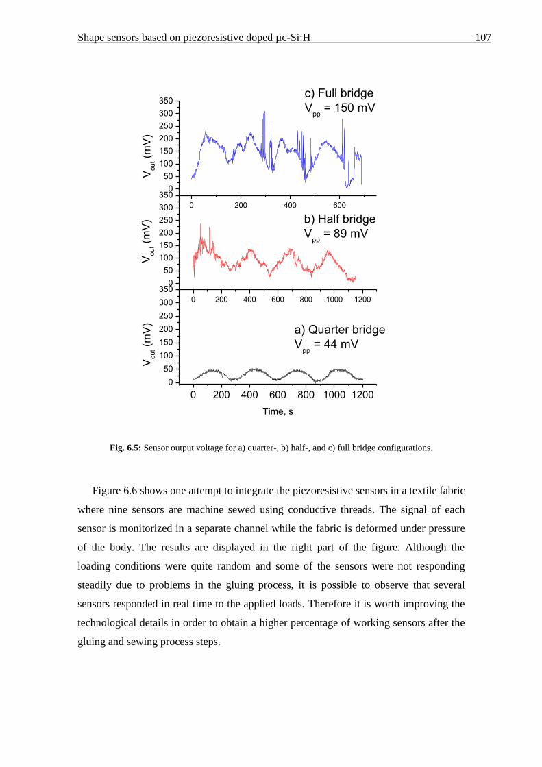
Shape sensors based on piezoresistive doped µc-Si:H 107
0 200 400 600 800 1000 1200
0
50
100
150
200
250
300
350
Vout (
mV
)
Time, s
a) Quarter bridge
Vpp
= 44 mV
0 200 400 600 800 1000 1200
0
50
100
150
200
250
300
350
Vout (
mV
) b) Half bridge
Vpp
= 89 mV
0 200 400 600
0
50
100
150
200
250
300
350c) Full bridge
Vpp
= 150 mV
Vout (
mV
)
Fig. 6.5: Sensor output voltage for a) quarter-, b) half-, and c) full bridge configurations.
Figure 6.6 shows one attempt to integrate the piezoresistive sensors in a textile fabric
where nine sensors are machine sewed using conductive threads. The signal of each
sensor is monitorized in a separate channel while the fabric is deformed under pressure
of the body. The results are displayed in the right part of the figure. Although the
loading conditions were quite random and some of the sensors were not responding
steadily due to problems in the gluing process, it is possible to observe that several
sensors responded in real time to the applied loads. Therefore it is worth improving the
technological details in order to obtain a higher percentage of working sensors after the
gluing and sewing process steps.
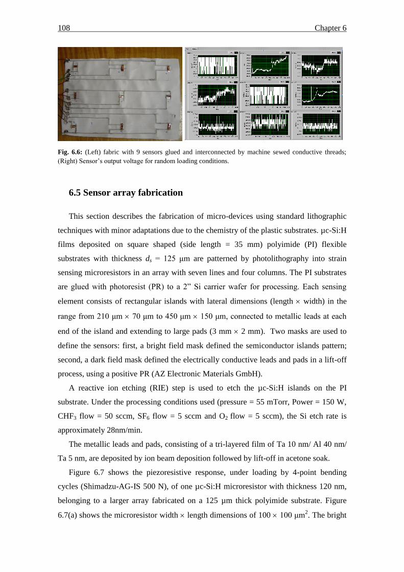
108 Chapter 6
Fig. 6.6: (Left) fabric with 9 sensors glued and interconnected by machine sewed conductive threads;
(Right) Sensor’s output voltage for random loading conditions.
6.5 Sensor array fabrication
This section describes the fabrication of micro-devices using standard lithographic
techniques with minor adaptations due to the chemistry of the plastic substrates. µc-Si:H
films deposited on square shaped (side length = 35 mm) polyimide (PI) flexible
substrates with thickness ds = 125 μm are patterned by photolithography into strain
sensing microresistors in an array with seven lines and four columns. The PI substrates
are glued with photoresist (PR) to a 2” Si carrier wafer for processing. Each sensing
element consists of rectangular islands with lateral dimensions (length width) in the
range from 210 μm 70 μm to 450 μm 150 μm, connected to metallic leads at each
end of the island and extending to large pads (3 mm 2 mm). Two masks are used to
define the sensors: first, a bright field mask defined the semiconductor islands pattern;
second, a dark field mask defined the electrically conductive leads and pads in a lift-off
process, using a positive PR (AZ Electronic Materials GmbH).
A reactive ion etching (RIE) step is used to etch the µc-Si:H islands on the PI
substrate. Under the processing conditions used (pressure = 55 mTorr, Power = 150 W,
CHF3 flow = 50 sccm, SF6 flow = 5 sccm and O2 flow = 5 sccm), the Si etch rate is
approximately 28nm/min.
The metallic leads and pads, consisting of a tri-layered film of Ta 10 nm/ Al 40 nm/
Ta 5 nm, are deposited by ion beam deposition followed by lift-off in acetone soak.
Figure 6.7 shows the piezoresistive response, under loading by 4-point bending
cycles (Shimadzu-AG-IS 500 N), of one µc-Si:H microresistor with thickness 120 nm,
belonging to a larger array fabricated on a 125 µm thick polyimide substrate. Figure
6.7(a) shows the microresistor width length dimensions of 100 100 μm2. The bright
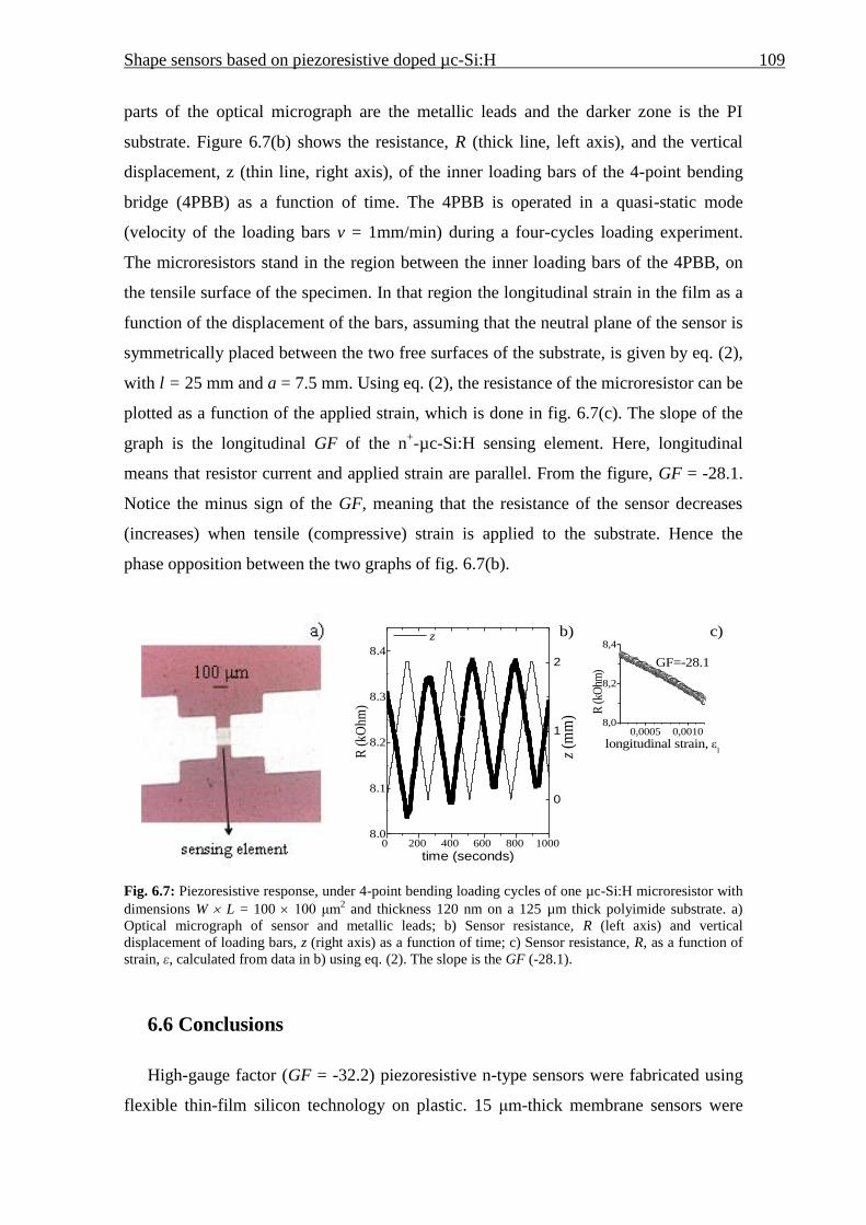
Shape sensors based on piezoresistive doped µc-Si:H 109
parts of the optical micrograph are the metallic leads and the darker zone is the PI
substrate. Figure 6.7(b) shows the resistance, R (thick line, left axis), and the vertical
displacement, z (thin line, right axis), of the inner loading bars of the 4-point bending
bridge (4PBB) as a function of time. The 4PBB is operated in a quasi-static mode
(velocity of the loading bars v = 1mm/min) during a four-cycles loading experiment.
The microresistors stand in the region between the inner loading bars of the 4PBB, on
the tensile surface of the specimen. In that region the longitudinal strain in the film as a
function of the displacement of the bars, assuming that the neutral plane of the sensor is
symmetrically placed between the two free surfaces of the substrate, is given by eq. (2),
with l = 25 mm and a = 7.5 mm. Using eq. (2), the resistance of the microresistor can be
plotted as a function of the applied strain, which is done in fig. 6.7(c). The slope of the
graph is the longitudinal GF of the n+-µc-Si:H sensing element. Here, longitudinal
means that resistor current and applied strain are parallel. From the figure, GF = -28.1.
Notice the minus sign of the GF, meaning that the resistance of the sensor decreases
(increases) when tensile (compressive) strain is applied to the substrate. Hence the
phase opposition between the two graphs of fig. 6.7(b).
Fig. 6.7: Piezoresistive response, under 4-point bending loading cycles of one µc-Si:H microresistor with
dimensions W L = 100 100 μm2 and thickness 120 nm on a 125 µm thick polyimide substrate. a)
Optical micrograph of sensor and metallic leads; b) Sensor resistance, R (left axis) and vertical
displacement of loading bars, z (right axis) as a function of time; c) Sensor resistance, R, as a function of
strain, ε, calculated from data in b) using eq. (2). The slope is the GF (-28.1).
6.6 Conclusions
High-gauge factor (GF = -32.2) piezoresistive n-type sensors were fabricated using
flexible thin-film silicon technology on plastic. 15 μm-thick membrane sensors were
0 200 400 600 800 10008.0
8.1
8.2
8.3
8.4
R (
kOhm
)
time (seconds)
0
1
2
c)b)
0,0005 0,00108,0
8,2
8,4
GF=-28.1
R (
kOhm
)
longitudinal strain, l
z
z (
mm
)

110 Chapter 6
batch fabricated and successfully transferred to large-area surfaces. This concept allows
to add sensing capabilities to many different materials and surfaces, namely to textiles.
The sensor’s output voltage using quarter-, half, and full-bridge configurations were
dynamically tested and the results follow the predictions made by circuit analysis for
conventional, rigid sensors. Nine sensors were incorporated in fabrics and
interconnected using machine sewed conductive threads. Their response to a random
distributed load is registered. Microresistors, with GF = -28.1, were fabricated on
plastic substrates using standard lithographic techniques.
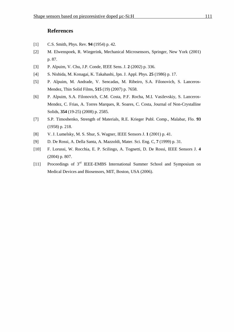
Shape sensors based on piezoresistive doped µc-Si:H 111
References
[1] C.S. Smith, Phys. Rev. 94 (1954) p. 42.
[2] M. Elwenspoek, R. Wiegerink, Mechanical Microsensors, Springer, New York (2001)
p. 87.
[3] P. Alpuim, V. Chu, J.P. Conde, IEEE Sens. J. 2 (2002) p. 336.
[4] S. Nishida, M. Konagai, K. Takahashi, Jpn. J. Appl. Phys. 25 (1986) p. 17.
[5] P. Alpuim, M. Andrade, V. Sencadas, M. Ribeiro, S.A. Filonovich, S. Lanceros-
Mendez, Thin Solid Films, 515 (19) (2007) p. 7658.
[6] P. Alpuim, S.A. Filonovich, C.M. Costa, P.F. Rocha, M.I. Vasilevskiy, S. Lanceros-
Mendez, C. Frias, A. Torres Marques, R. Soares, C. Costa, Journal of Non-Crystalline
Solids, 354 (19-25) (2008) p. 2585.
[7] S.P. Timoshenko, Strength of Materials, R.E. Krieger Publ. Comp., Malabar, Flo. 93
(1958) p. 218.
[8] V. J. Lumelsky, M. S. Shur, S. Wagner, IEEE Sensors J. 1 (2001) p. 41.
[9] D. De Rossi, A. Della Santa, A. Mazzoldi, Mater. Sci. Eng. C, 7 (1999) p. 31.
[10] F. Lorussi, W. Rocchia, E. P. Scilingo, A. Tognetti, D. De Rossi, IEEE Sensors J. 4
(2004) p. 807.
[11] Proceedings of 3rd
IEEE-EMBS International Summer School and Symposium on
Medical Devices and Biosensors, MIT, Boston, USA (2006).

112 Chapter 6
Chapter 7
7 Conclusions
This work showed that it is possible to deposit µc-Si:H and a-Si:H thin films on low
temperature plastics at high deposition rates, while keeping up the electronic quality for
application in flexible thin-film silicon solar cells and other devices.
Flexible single junction solar cells were successfully fabricated on transparent (PEN)
and opaque (PI) plastic substrates at low temperatures of 150ºC for PEN and 200ºC for
PI. The p-i-n superstrate configuration was used for solar cells on PEN and efficiencies
of ~5% were achieved. In the case of PI, solar cell efficiencies of around 7.5% were
obtained using n-i-p substrate configuration. Different light trapping strategies were
developed for transparent and opaque substrates. Laser texturing of PET substrates was
studied and wet-chemical etching of the TCO back contact was applied for solar cells on
PI.
Also, flexible piezoresistive sensors with high gauge factor have been fabricated on
very thin (15 µm) PI films and on thicker ones (125 µm). These 15 µm sensors were
transferred to large area surfaces and incorporated in textiles in an attempt of a smart
textile prototype. The main conclusions of this thesis are summarized in the following
paragraphs.
7.1 High-rate deposition of silicon thin films on plastics
The deposition rate of both µc-Si:H and a-Si:H thin films can be increased
consistently by: 1) decreasing the inter electrode distance, 2) increasing the deposition
pressure, and 3) increasing the rf-power. The deposition rate decreases as the HD
increases in all deposition conditions. For each pressure and rf-power used, there is a
114 Chapter 7
value of hydrogen dilution of silane for which the films undergo an amorphous-to-
microcrystalline phase transition. The exact concentration of H2 required for this
transition to occur is a function of the deposition parameters and it increases when the
working pressure increases, keeping other parameters constant. The films deposited at 6
Torr and 20 W had the highest microcrystalline deposition rate (rd = 0.38 nm/s). The
films with high photosensitivity (>105) are amorphous. The best µc-Si:H had
photosensitivity around 102. The best mixed phase film was obtained at 6 Torr, 20 W
and had photosensitivity in excess of 103. n- and p-type µc-Si:H films were obtained
with σdk = 7.8 and 0.87 Ω-1
cm-1
, respectively. At 6 Torr, it was not possible to obtain
highly doped microcrystalline films. n-type conductivity was 10-3
Ω-1
cm-1
while p-type
σdk= 510-7
Ω-1
cm-1
.
7.2 Flexible thin film silicon solar cells
Flexible amorphous superstrate p-i-n solar cells were fabricated on PEN with
efficiencies of ~4.5 - 5%, and substrate n-i-p solar cells on PI with efficiencies of ~6 –
6.5%. In both cases, texturing schemes for light trapping were absent and the
efficiencies were limited by low current-densities and low fill factors, with high series
resistances.
Microcrystalline single-junction n-i-p thin film silicon solar cells on flexible smooth
polyimide substrate showed similar behavior in terms of performance parameters in
comparison to cells deposited on smooth glass. The Voc was around 20-40 mV lower for
the cells on PI, which is related to higher i-layer crystallinity of cells on PI. A textured
ZnO:Ga layer was developed to promote light trapping in the solar cells on PI that yield
more than 23 mA/cm2 on absorbers of 1.8 µm thickness with cell efficiencies of up to
7.5%.
Laser texturing of plastic substrates increased dramatically the scattered
transmittance (from 1.5 to >40%) and scattered reflectance (from 3 to 30%). However,
the total transmittance and total reflectance decreased markedly in both cases.
Conclusions 115
7.3 Flexible µc-Si:H piezoresistive sensors
High-gauge factor (GF = -32.2) piezoresistive n-type sensors were fabricated using
flexible thin-film silicon technology on plastic. 15 μm-thick membrane sensors were
batch fabricated and successfully transferred to large-area surfaces. This concept allows
to add sensing capabilities to many different materials and surfaces, namely to textiles.
The sensor’s output voltage using quarter-, half, and full-bridge configurations were
dynamically tested and the results follow the predictions made by circuit analysis for
conventional, rigid sensors. Nine sensors were incorporated in fabrics and
interconnected using machine sewed conductive threads. Their response to a random
distributed load was registered. Microresistors, with GF = -28.1, were fabricated on
plastic substrates using standard lithographic techniques.