Embed Size (px)
Citation preview

Purpose
• This course discusses techniques for analyzing and eliminating noise in microcontroller (MCU) and microprocessor (MPU) based embedded systems.
Objectives
• Learn about a method for performing a system-level EMI test.
• See how to evaluate current balance.
• Gain a basic knowledge of tests for measuring the emissions fromLSI devices that can be used for product selection.
Content
• 18 pages
Learning Time
30 minutes
Course Introduction

Reducing EMI
EMI reduction is a goal shared by both
the semiconductor experts who design
MPUs and other LSI devices, and by the engineers who apply those chips in embedded systems
ECU Electronic Control Unit
EMI Electromagnetic Interference
Explanation of Terms
A microcontroller chip is composed of a core, I/O ports, and power supply circuitry. The core consists of the CPU, ROM, RAM, and blocks implementing timers, communication, and analog functions.
Power supply
Two power supplies are applied to the LSI: Vcc and Vss. The core power supply internal to the LSI is VCL (internal step-down). The Vss-based power supply routed through the LSI is VSL.
Harness Cables (wires) connecting a board and power supply or connecting one unit in a system to another
Balun
LISN
TEM Cell
WBFC
Core
A room designed to block radiation from the outside and to minimize reflections off the room’s walls, ceiling, and floor
A passive electronic device that converts between balanced and unbalanced electrical signals
CISPR 25 International Special Committee on Radio Interference (CISPR) publication 25: “Limits and methods of measuring radio disturbance characteristics for the protection of receivers on board vehicles.” CISPR is a sub-committee of the International Electrotechnical Commission (IEC).
Line Impedance Stabilization Network
Transverse Electromagnetic Cell
Workbench Faraday Cage
Anechoicchamber

• System-level evaluation
- Example: performed on three test boards
- Test method for measuring emissions from wiring harness: (CISPR 25
equivalent)
• Radiation levels ranged from high for board A to low for board C
Radiation from Wiring Harness
Test setup
LISN
Antenna
Circuit board with MPU
Harness
Anechoic chamber Board B
Board C
Board A

• Near-field distribution was measured also, using an EMV-200 test system
- A sensor coil on a probe rotatesand moves with precision in three dimensions to scan and recordthe EMI radiated from the circuit board
• Data from the CISPR 25 test and the EMV-200 scan was used to examine the correspondence between the field strength and system level evaluation at the connector position
EMI from Circuit Board
EMV-200
Probe with sensor coil
Data from near-field scan
MPU
Power supply connector
Circuit board
f = 80MHz

Emission Measurement Results
• With probe above the harness connector, there is a direct relationship between the antenna and near-field probe readings
- Using a low-emissions MCU reduces emissions at the wiring harness
connector on the board
• Moving from a 2-layer board to a 4-layer board further reduces emissions at the wiring harness connector
Harness mounting area
MCU
Board B
@80 MHzHarness mounting
area MCU
Board C
@80MHz
Harness mounting area
MCU
Board A
Directly above MCU
Above harness mounting area

Evaluating Current Balance in PCB
- Test board provides extra pads to which 470Ωresistors can be connected to divert current through loops on left and right, creating differences between the signal and return currents in the area highlighted by the pink oval
- Near-field scan data of the entire board was obtained for three test cases:
• Case 1: No resistors were connected, so currents in measurement area were
balanced
• Case 2: a 470Ω resistor was connected on left
side of board, creating a 10% current unbalance
in the measurement area
• Case 3: Two 470Ω resistors were connected on
the left and right sides of the board, creating
Near-field measurements show the common-mode radiation caused by unbalanced currents flowing in the circuit board
Left loop Right loop
Line width = 1.3mm
Termination(50Ω)
Pads
100, 90 or 80%
100%
Area in which a difference between the signal current and return current can be created

h = 2.5mm
f = 80MHz
Case 1: Current Balanced
With no 470Ω resistors
connected, current was balanced, so minimum levels of EMI were detected when the EMV-200’s probe scanned the measurement area of the printed circuit board
Case A
100%
100%
No 470Ω resistors(Both loops open)
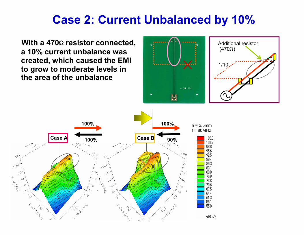
Case 2: Current Unbalanced by 10%
With a 470Ω resistor connected,
a 10% current unbalance was created, which caused the EMI to grow to moderate levels in the area of the unbalance
Case BCase A
h = 2.5mm
f = 80MHz
100%
100%
100%
90%
Additional resistor(470Ω)
1/10

Case 3: Current Unbalanced by 20%
With both 470Ω resistors
connected, a 20% current unbalance created; this caused the EMI to becomes high in the area of the unbalance
Case B Case CCase A
h = 2.5mm
f = 80MHz
100%
100%
100%
90%
100%
80%
Two additional resistors (470Ω)
1/10
1/10
Near-field scans can help locate the cause of EMI
problems

Board Layout Affects Emissions
Terminated
Microstrip line
Reference Microstrip Line
Signal input:
100MHz sine wave, 1.0Vp-p )
An ideal microstrip line shows a fairly uniform current distribution and minimum emissions
Pitch: 5mm; Scan height: 10mm
Scanned from bottom side (reference plane)
@100MHz

Layout Affects Emissions — 2
Symmetric Pattern
Emissions increase as the width of the pc board becomes more narrow
Pitch: 5mm; Scan height: 10mm
Scanned from bottom side (reference plane)
@100MHz
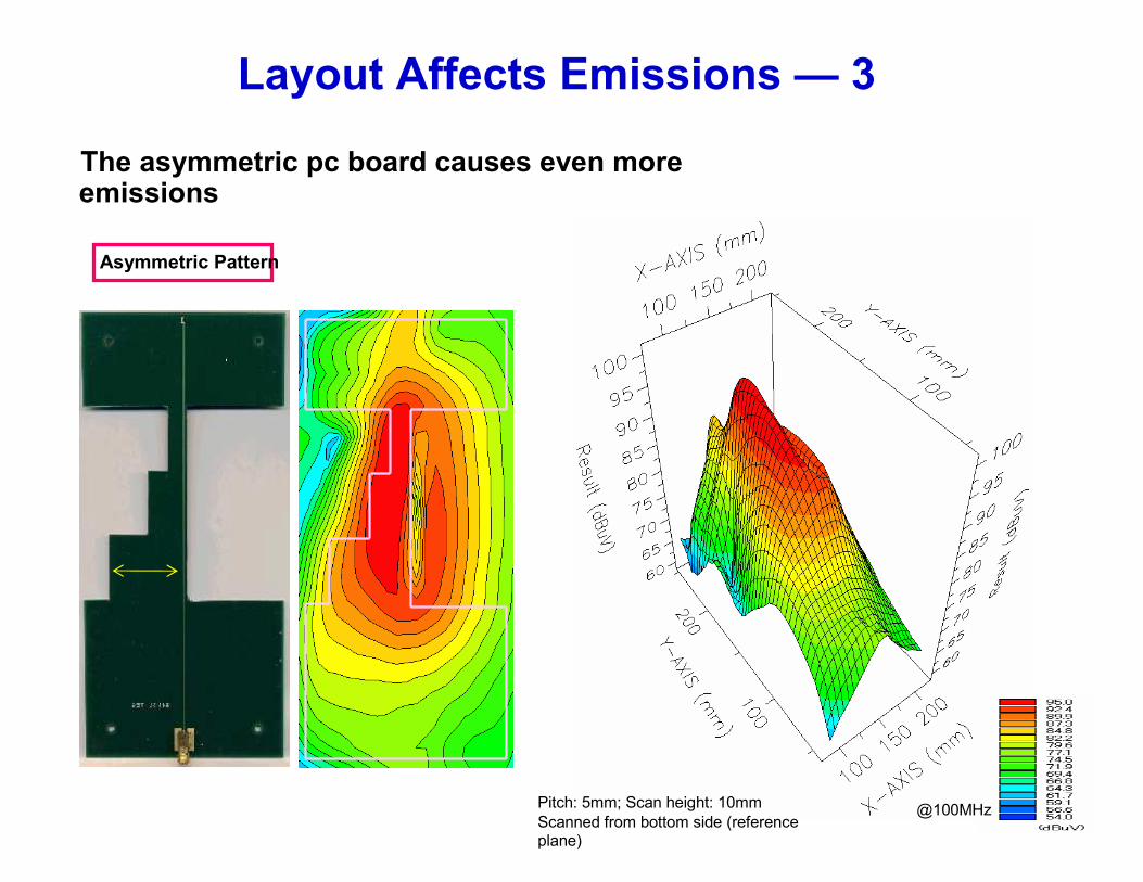
Layout Affects Emissions — 3
Asymmetric Pattern
The asymmetric pc board causes even more emissions
Pitch: 5mm; Scan height: 10mm
Scanned from bottom side (reference plane)
@100MHz

Emission Measurement Standards
The international standards listed here are used to measure electromagnetic emissions* from MCUs and other ICs
Standard No.: Title Latest StandardDocument Issue
Date Remarks
IEC 61967-1: General conditions and definitions 2002-03-12
IS[IEC 61967-1]
IEC 61967-2: Measurement of radiated emissions,
TEM-cell and wideband TEM-cell
Method
2005-09 IS[IEC 61967-2]
2005-06 TS[IEC TS 61967-3]
2002-04-30
IS[IEC 61967-4]
2002-06-25
IS[IEC 61967-6]
IEC 61967-3: Measurement of radiated emissions,
Surface Scan Method (Technical
Specifications)IEC 61967-4: Measurement of conducted emissions,
1-ohm/50-ohm Direct Coupling Method [IEC 61967-4 Ed. 1.1]
2006-2007Edition 1.1
2003-01-17
IS[IEC 61967-5]IEC 61967-5: Measurement of conducted emissions,
Workbench Faraday Cage Method
IEC 61967-6: Measurement of conducted emissions,
Magnetic Probe Method
IS: IEC International Standard TS: Technical Specification*Measurement range: 150kHz to 1GHz
IC
Vcc
49Ω
1Ω 50Ωin IC
Vcc
50Ω
in
IC
Vcc
950Ω
50Ω1K Ohmex.
vn
IS IS
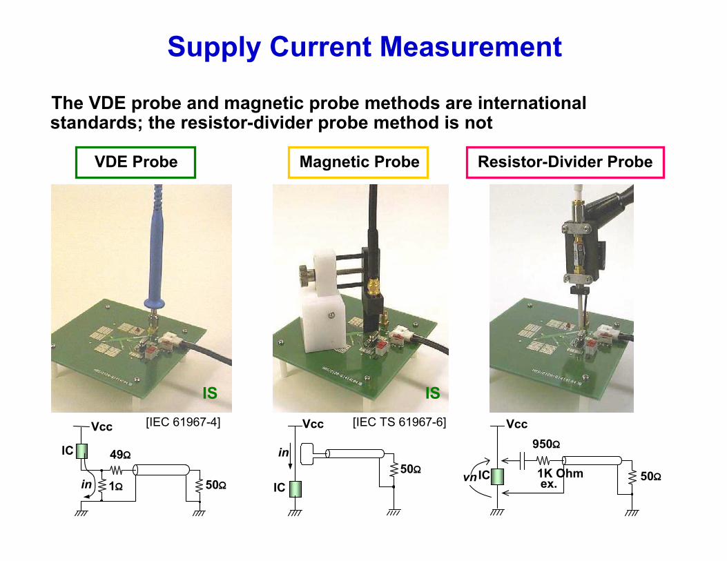
Supply Current Measurement
The VDE probe and magnetic probe methods are international standards; the resistor-divider probe method is not
VDE Probe Magnetic Probe Resistor-Divider Probe
[IEC TS 61967-6][IEC 61967-4]
IS
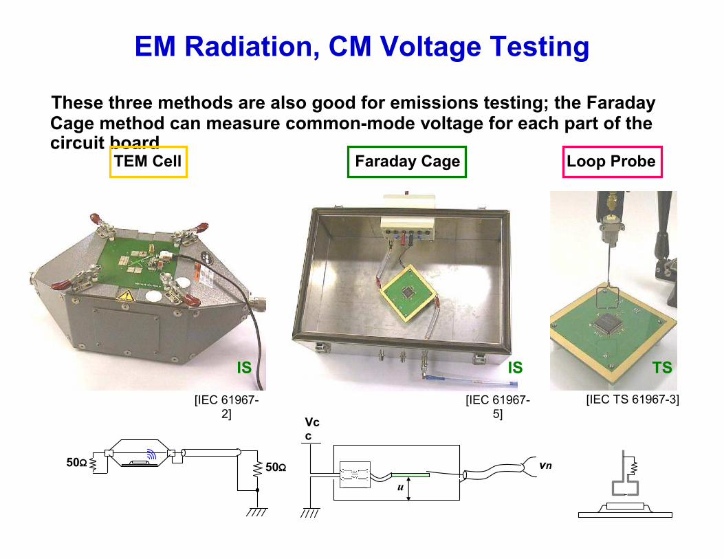
EM Radiation, CM Voltage Testing
These three methods are also good for emissions testing; the Faraday Cage method can measure common-mode voltage for each part of the circuit board
Faraday Cage Loop Probe
u
Vcc
vn
[IEC 61967-5]
[IEC TS 61967-3]
TS
50Ω 50Ω
TEM Cell
[IEC 61967-2]
IS

Problem with Normal TEM Cell
When measuring emissions from LSI devices, the combined EM field data are almost identical to that of the magnetic field measurement alone; the electric field data is difficult to see
Magnetic field
Electric field + Magnetic field
(combined result produced
by a normal TEM cell measurement)
TEM cell output level (dB)
Frequency (MHz)
TEM cell method (normal)
Terminator Measuring system
50Ω 50Ω
TEM Cell
Electric field

Electric field coupling
(50Ω terminator)
50Ω terminator
(magnetic field coupling)
Output
Renesas “Hybrid Balun”
Applying the TEM Cell Method
With the “hybrid balun” that Renesas has adopted, voltages proportional to a pure electric field and a pure magnetic field can be obtained• Photo shows an electric field coupling
• Changing the terminator and output port results in a magnetic field coupling
System-level evaluation techniques
Importance of circuit board layout
Methods for evaluating emissions from LSI devices
Course Summary
For more information on specific devices and related
support products and material, please visit our Web site:
http://america.renesas.com