Embed Size (px)
Citation preview
- 1 -CS - ES
Embedded Systems
- 2 -CS - ES
Embedded Systems
End-of-term exam, Monday February 14, 2011, 14-17
End-of-semester exam : Tuesday March 22, 2011, 14-17
Final grade:
best grade in end-of-term or end-of-semester exam.
- 3 -CS - ES
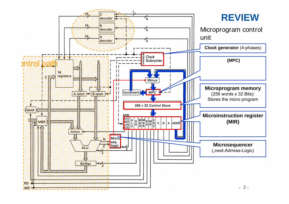
Microprogram control unit
ontrol path
Microinstruction register(MIR)
Clock generator (4-phases)
(MPC)
Microsequencer(„next-Adrress-Logic)
Microprogram memory(256 words x 32 Bits):
Stores the micro program
REVIEW
- 4 -CS - ES
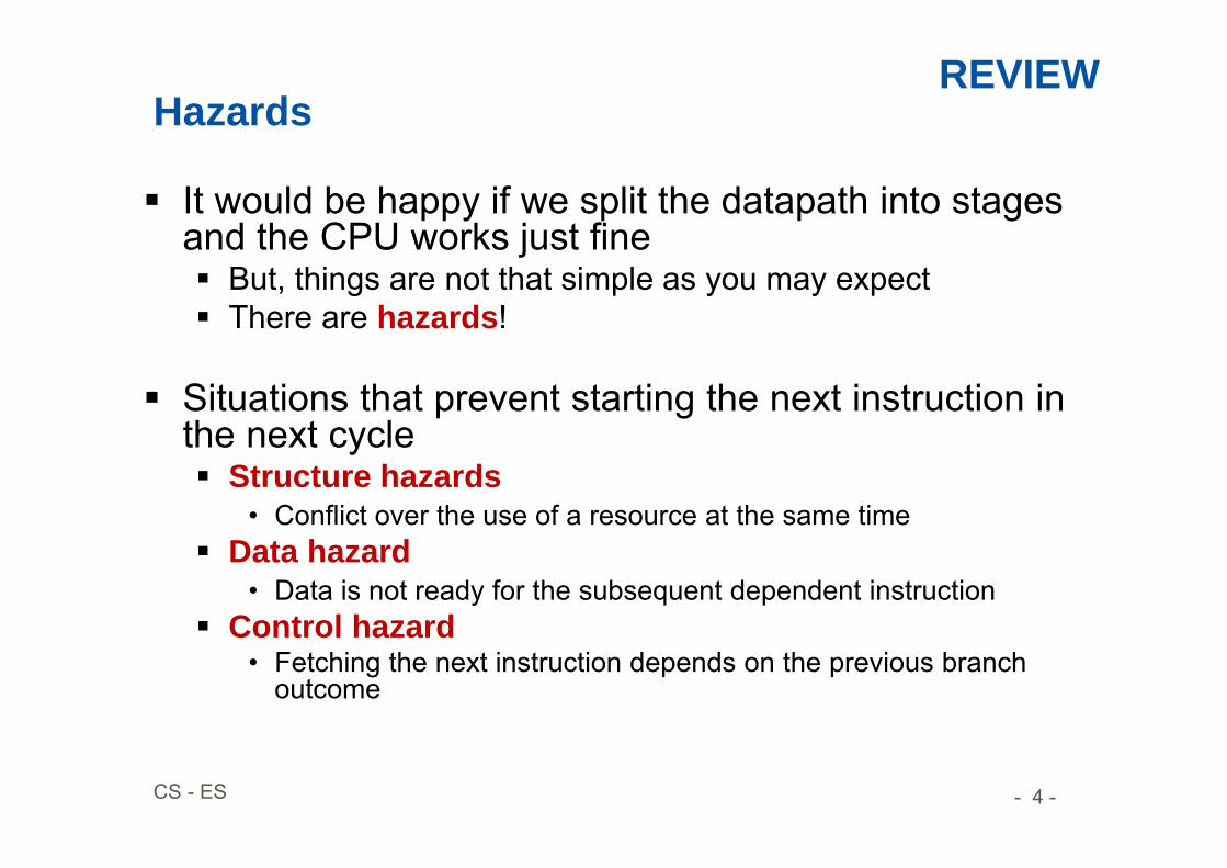
Hazards
It would be happy if we split the datapath into stages and the CPU works just fine But, things are not that simple as you may expect There are hazards!
Situations that prevent starting the next instruction in the next cycle Structure hazards
• Conflict over the use of a resource at the same time Data hazard
• Data is not ready for the subsequent dependent instruction Control hazard
• Fetching the next instruction depends on the previous branch outcome
REVIEW
- 5 -CS - ES
REVIEW
• Requirements• Model-based design• Safety• FlexRay

- 6 -CS - ES
From Architecture to Application
Timing behavior has to be predictable Features that cause problems:
• Unpredictable access to shared resources: caches, pipeline (bubbles), communication times (e.g.; multiprocessors)
• Branch prediction, Interrupts, Instructions that with data-dependent execution times
Trying to avoid as many of these as possible.
Timing analysis lecture next week
- 7 -CS - ES
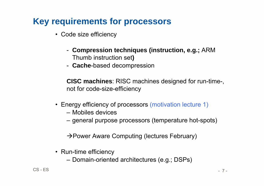
Key requirements for processors• Code size efficiency
- Compression techniques (instruction, e.g.; ARM Thumb instruction set)
- Cache-based decompression
CISC machines: RISC machines designed for run-time-,not for code-size-efficiency
• Energy efficiency of processors (motivation lecture 1)– Mobiles devices– general purpose processors (temperature hot-spots)
Power Aware Computing (lectures February)
• Run-time efficiency– Domain-oriented architectures (e.g.; DSPs)
- 8 -CS - ES
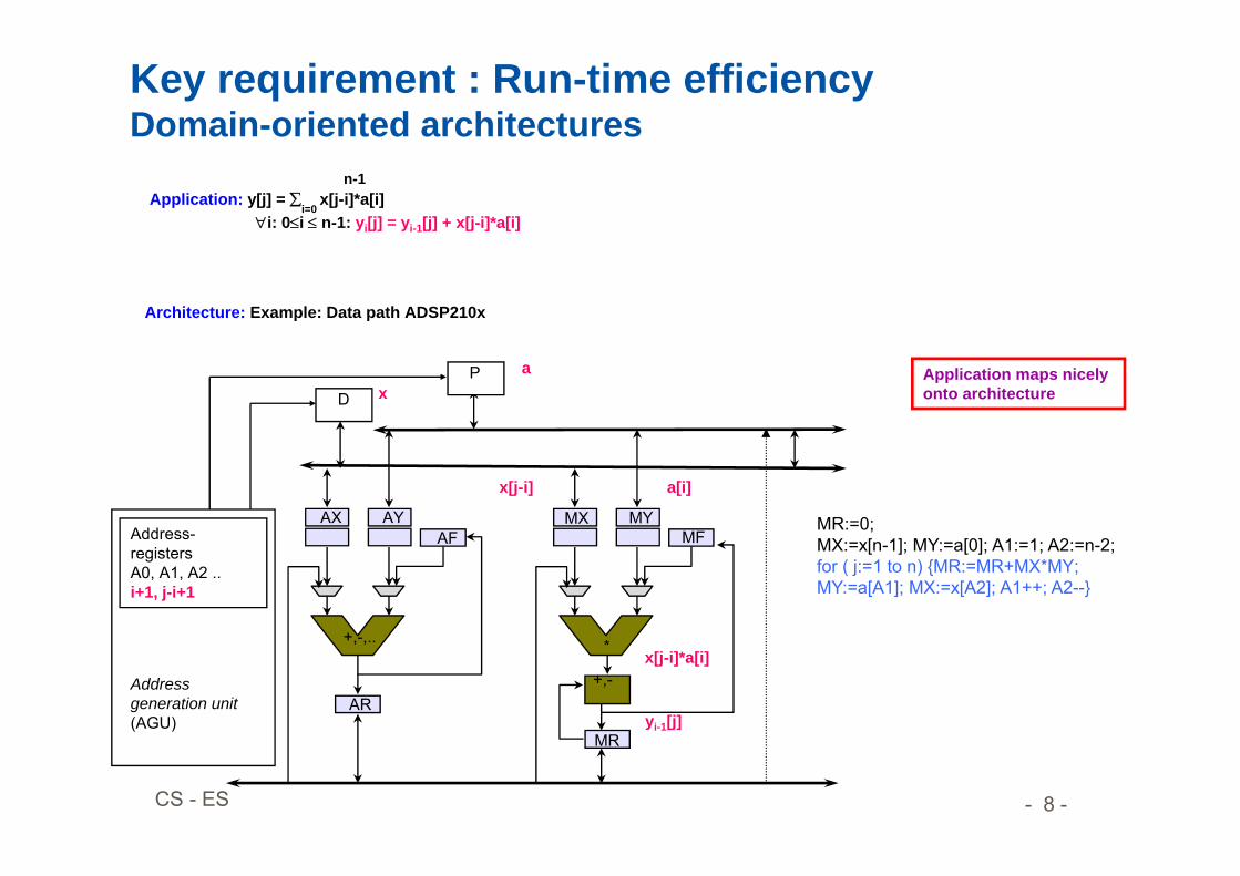
Application: y[j] = i=0
x[j-i]*a[i] i: 0i n-1: yi[j] = yi-1[j] + x[j-i]*a[i]
Key requirement : Run-time efficiencyDomain-oriented architectures
Architecture: Example: Data path ADSP210x
n-1
Application maps nicely onto architecture
MR
MFMX MY
*
+,-AR
AFAX AY
+,-,..
DP
yi-1[j]
x[j-i]
x[j-i]*a[i]
a[i]
Address generation unit(AGU)
Address-registersA0, A1, A2 ..i+1, j-i+1
ax
MR:=0;MX:=x[n-1]; MY:=a[0]; A1:=1; A2:=n-2; for ( j:=1 to n) {MR:=MR+MX*MY; MY:=a[A1]; MX:=x[A2]; A1++; A2--}

- 9 -CS - ES
DSP-Processors: multiply/accumulate (MAC)and zero-overhead loop (ZOL) instructions
MR:=0; A1:=1; A2:=n-2; MX:=x[n-1]; MY:=a[0];for ( j:=1 to n){MR:=MR+MX*MY; MY:=a[A1]; MX:=x[A2]; A1++; A2--}
Multiply/accumulate (MAC) instruction Zero-overhead loop (ZOL) instruction preceding MAC instruction.Loop testing done in parallel to MAC operations.
Loop counter incr., test againstend condition, and branching aredone by hardware
- 10 -CS - ES
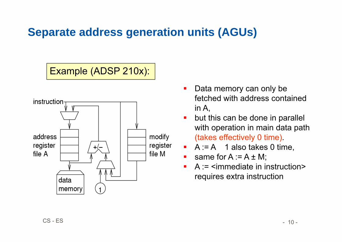
Separate address generation units (AGUs)
Data memory can only be fetched with address contained in A,
but this can be done in parallel with operation in main data path (takes effectively 0 time).
A := A 1 also takes 0 time, same for A := A ± M; A := <immediate in instruction>
requires extra instruction
Example (ADSP 210x):

- 11 -CS - ES
Returns largest/smallest number in case of over/underflows
Example:a 0111b + 1001standard wrap around arithmetic (1)0000saturating arithmetic 1111(a+b)/2: correct 1000
wrap around arithmetic 0000saturating arithmetic + shifted 0111
Appropriate for DSP/multimedia applications:• No timeliness of results if interrupts are generated for overflows• Precise values less important• Wrap around arithmetic would be worse.
Saturating arithmetic
„almost correct“

- 12 -CS - ES
Key idea of very long instruction word (VLIW) computers
Instructions included in long instruction packets.Instruction packets are assumed to be executed in parallel.
Fixed association of packet bits with functional units.
- 13 -CS - ES
Very long instruction word (VLIW) architectures
Very long instruction word (“instruction packet”) contains several instructions, all of which are assumed to be executed in parallel.
Compiler is assumed to generate these “parallel” packets Complexity of finding parallelism is moved from the hardware
(RISC/CISC processors) to the compiler; Ideally, this avoids the overhead (silicon, energy, ..) of identifying parallelism at run-time.
A lot of expectations into VLIW machines
Explicitly parallel instruction set computers (EPICs) are an extension of VLIW architectures: parallelism detected by compiler, but no need to encode parallelism in 1 word.
- 14 -CS - ES
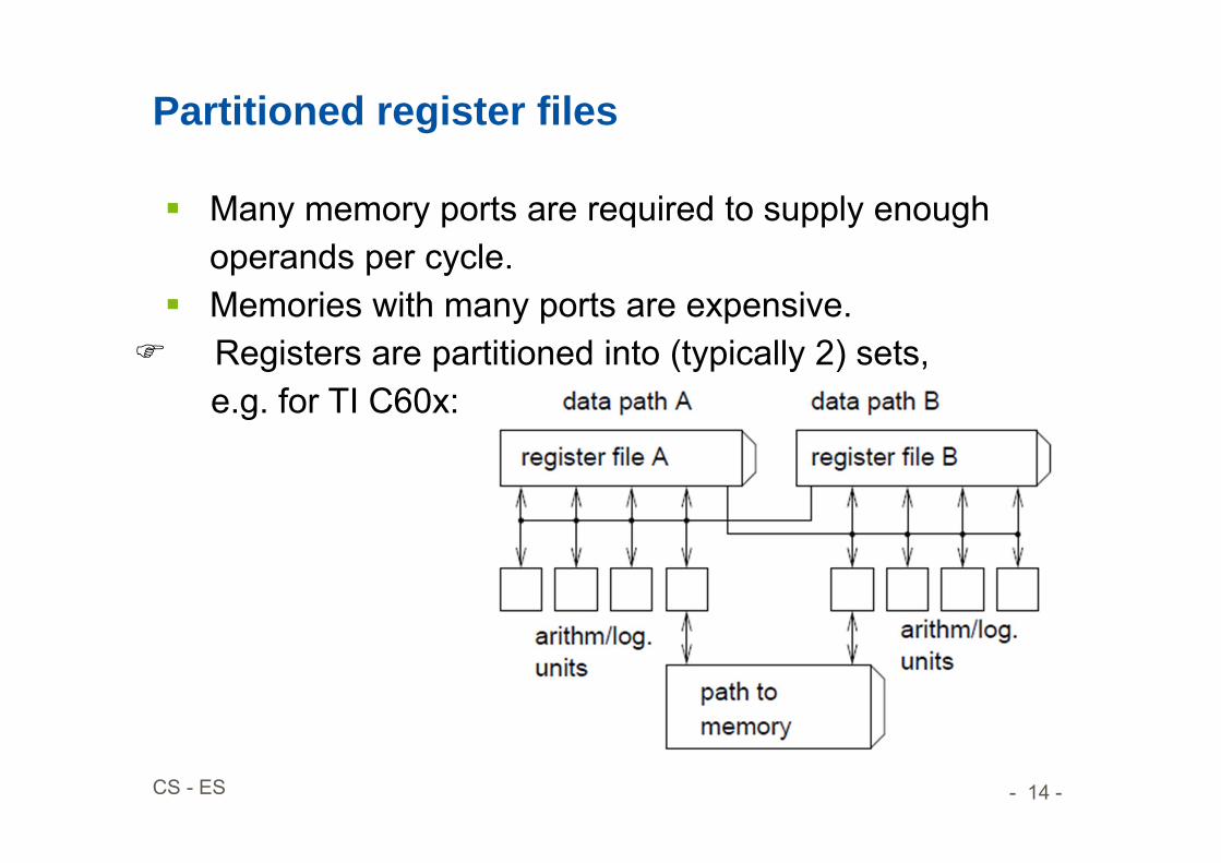
Partitioned register files
Many memory ports are required to supply enough operands per cycle.
Memories with many ports are expensive. Registers are partitioned into (typically 2) sets,
e.g. for TI C60x:
- 15 -CS - ES
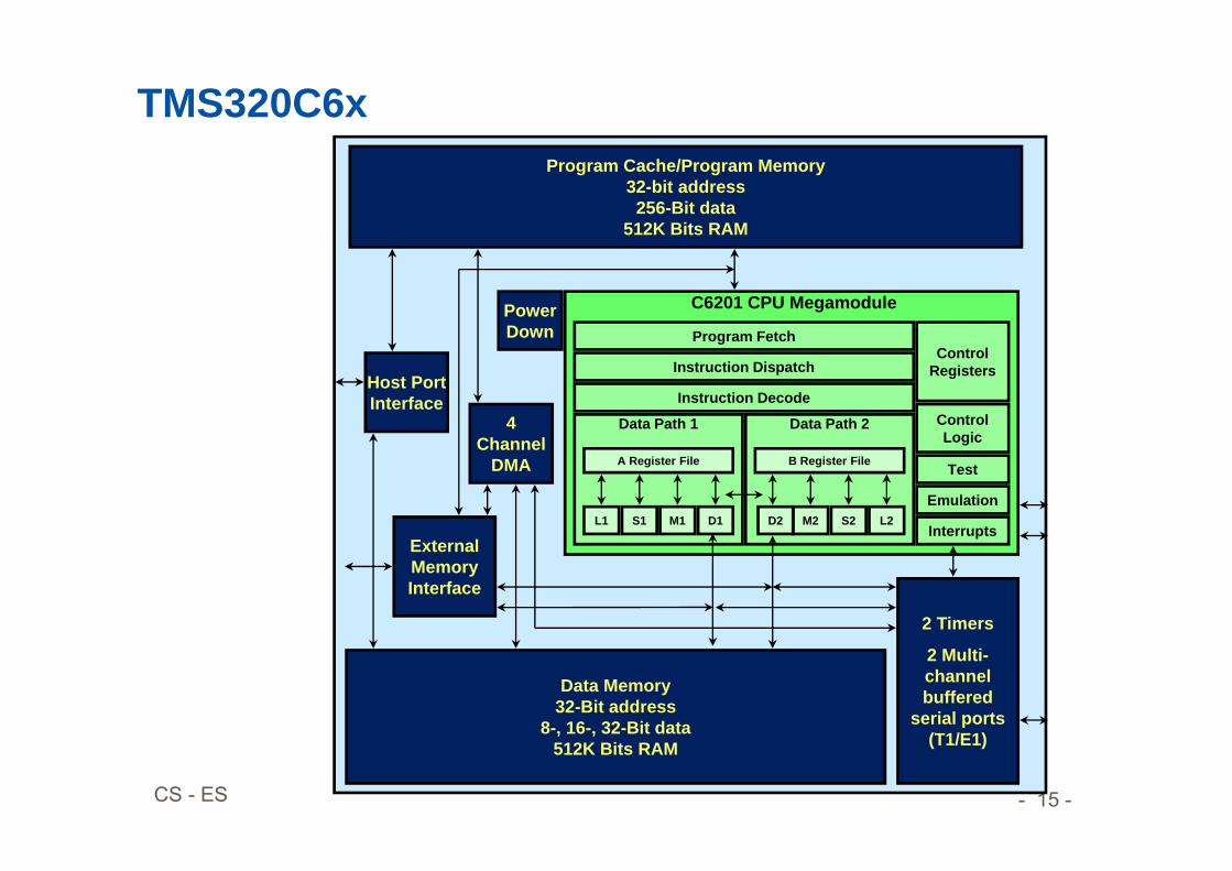
TMS320C6x
C6201 CPU Megamodule
Data Path 1
D1M1S1L1
A Register File
Data Path 2
L2S2M2D2
B Register File
Instruction Decode
Instruction Dispatch
Program Fetch
Interrupts
Control Registers
Control Logic
Emulation
Test
External Memory Interface
4 Channel
DMA
Program Cache/Program Memory32-bit address
256-Bit data512K Bits RAM
Host Port Interface
2 Timers
2 Multi-channel buffered
serial ports (T1/E1)
Data Memory32-Bit address
8-, 16-, 32-Bit data512K Bits RAM
Power Down
- 16 -CS - ES
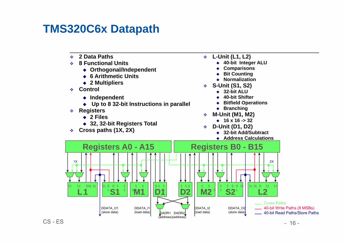
TMS320C6x Datapath
Cross Paths40-bit Write Paths (8 MSBs)40-bit Read Paths/Store Paths
M2
Registers B0 - B15
L2S2
DDATA_I2(load data)
S2D
DL
SLSL D DLS2
S1
S1
S2D2
DS1
S2
D
M1
Registers A0 - A15
L1 S1S1 S2
DDL
SL SLDDL S2
S1
S1
S2 D1
D S1
S2
D
DDATA_O2(store data)DADR2
(address)DADR1
(address)
DDATA_I1(load data)
DDATA_O1(store data)
2X1X
2 Data Paths 8 Functional Units
Orthogonal/Independent 6 Arithmetic Units 2 Multipliers
Control Independent Up to 8 32-bit Instructions in parallel
Registers 2 Files 32, 32-bit Registers Total
Cross paths (1X, 2X)
L-Unit (L1, L2) 40-bit Integer ALU Comparisons Bit Counting Normalization
S-Unit (S1, S2) 32-bit ALU 40-bit Shifter Bitfield Operations Branching
M-Unit (M1, M2) 16 x 16 -> 32
D-Unit (D1, D2) 32-bit Add/Subtract Address Calculations
S1
- 17 -CS - ES
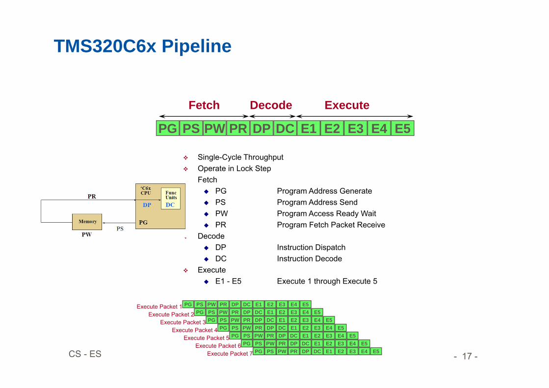
TMS320C6x Pipeline
Single-Cycle Throughput Operate in Lock Step Fetch
PG Program Address Generate PS Program Address Send PW Program Access Ready Wait PR Program Fetch Packet Receive
Decode DP Instruction Dispatch DC Instruction Decode
Execute E1 - E5 Execute 1 through Execute 5
Fetch Decode Execute
PG PS PW PR DP DC E1 E2 E3 E4 E5PG PS PW PR DP DC E1 E2 E3 E4 E5
PG PS PW PR DP DC E1 E2 E3 E4 E5PG PS PW PR DP DC E1 E2 E3 E4 E5
PG PS PW PR DP DC E1 E2 E3 E4 E5PG PS PW PR DP DC E1 E2 E3 E4 E5
PG PS PW PR DP DC E1 E2 E3 E4 E5
PG PS PW PR DP DC E1 E2 E3 E4 E5
Execute Packet 1Execute Packet 2
Execute Packet 3Execute Packet 4
Execute Packet 5Execute Packet 6
Execute Packet 7
- 18 -CS - ES
PG PS PW PR DP DCPG PS PW PR DP
PG PS PW PRPG PS PW
PG PS
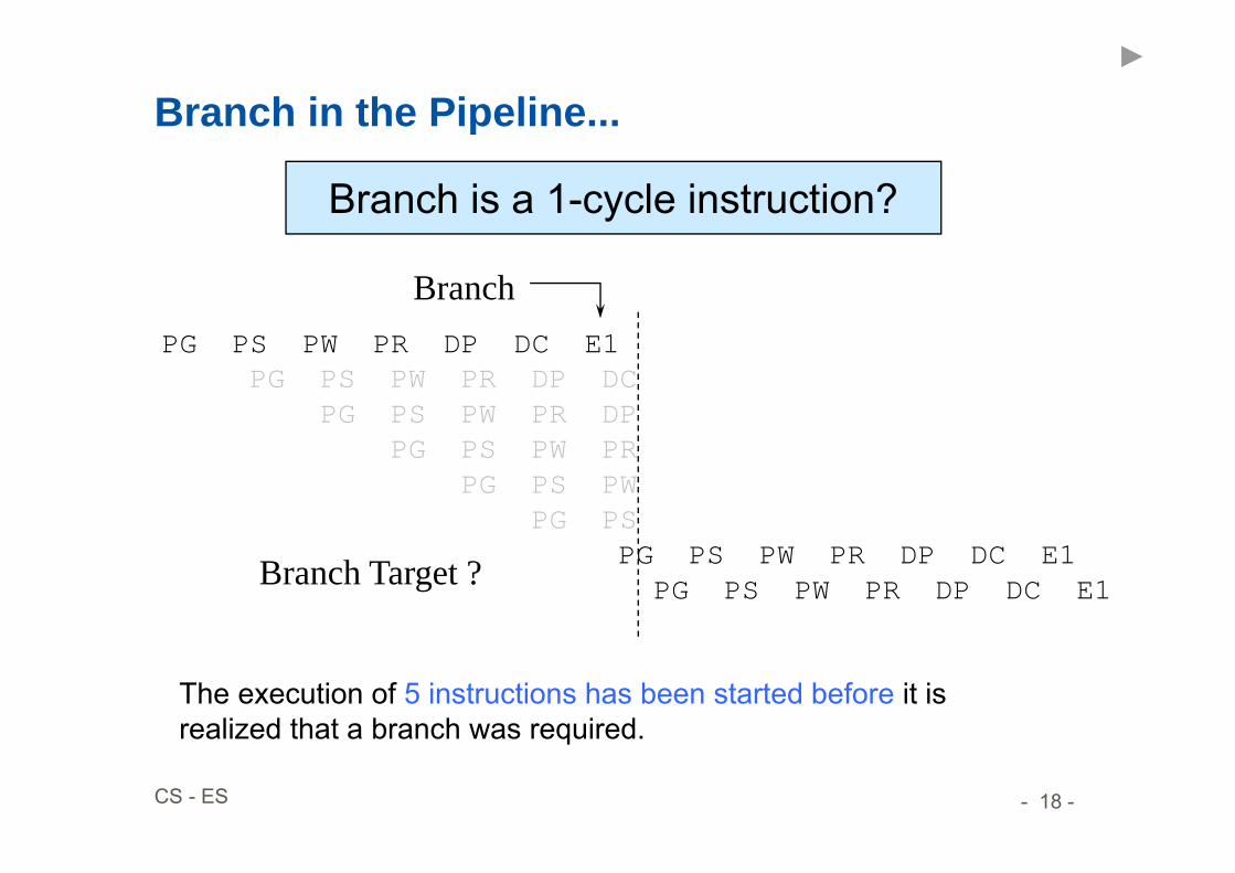
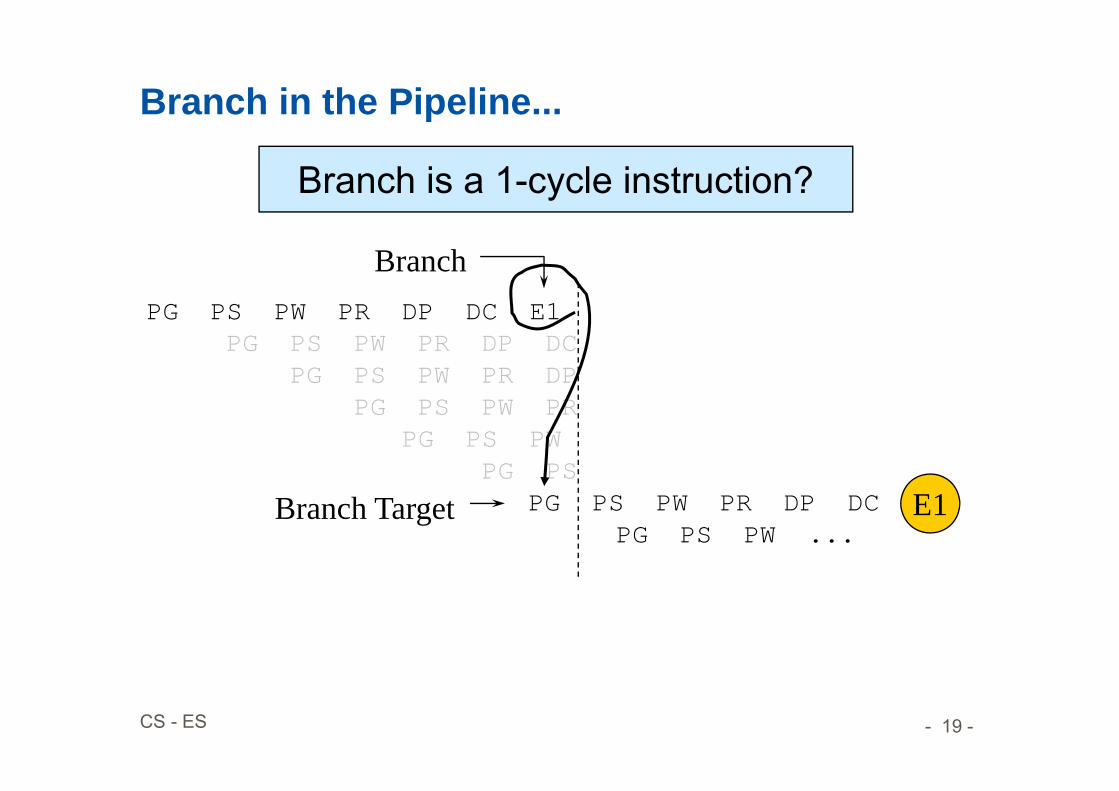
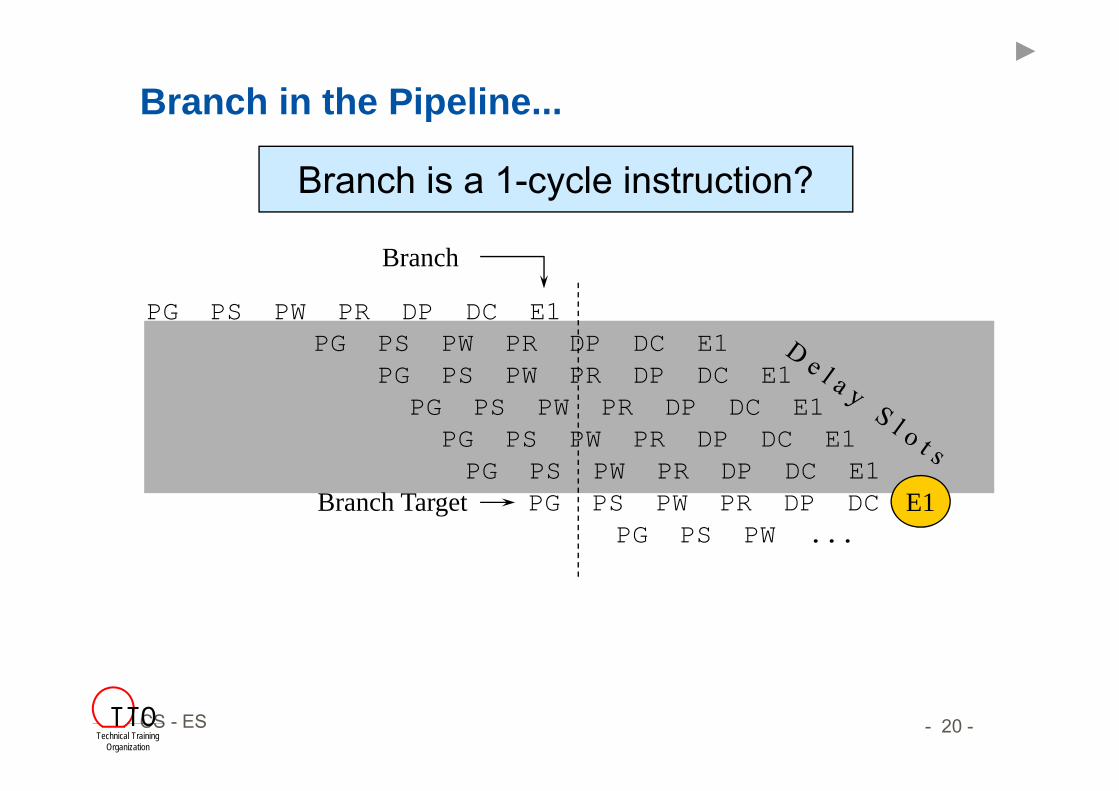
Branch in the Pipeline...
Branch is a 1-cycle instruction?
PG PS PW PR DP DC E1
Branch
PG PS PW PR DP DC E1PG PS PW PR DP DC E1Branch Target ?
The execution of 5 instructions has been started before it is realized that a branch was required.
- 19 -CS - ES
PG PS PW PR DP DCPG PS PW PR DP
PG PS PW PRPG PS PW
PG PS
PG PS PW PR DP DC E1
Branch in the Pipeline...
Branch
PG PS PW PR DP DCPG PS PW ...
Branch Target E1
Branch is a 1-cycle instruction?
- 20 -CS - ES
PG PS PW PR DP DC E1 PG PS PW PR DP DC E1
PG PS PW PR DP DC E1PG PS PW PR DP DC E1PG PS PW PR DP DC E1
PG PS PW PR DP DC E1
Branch in the Pipeline...
Branch
PG PS PW PR DP DCPG PS PW ...
Branch Target E1
Branch is a 1-cycle instruction?
Technical TrainingOrganization
TTO
- 21 -CS - ES
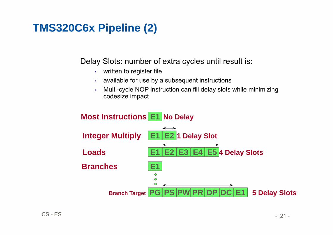
TMS320C6x Pipeline (2)
Delay Slots: number of extra cycles until result is:• written to register file• available for use by a subsequent instructions• Multi-cycle NOP instruction can fill delay slots while minimizing
codesize impact
E1
E1 E2
E1
Most Instructions
Integer Multiply
Loads
Branch Target
No Delay
1 Delay Slot
4 Delay Slots
5 Delay Slots
E2 E3 E4 E5
E1
PG PS PW PR DP DC
Branches
E1
- 22 -CS - ES
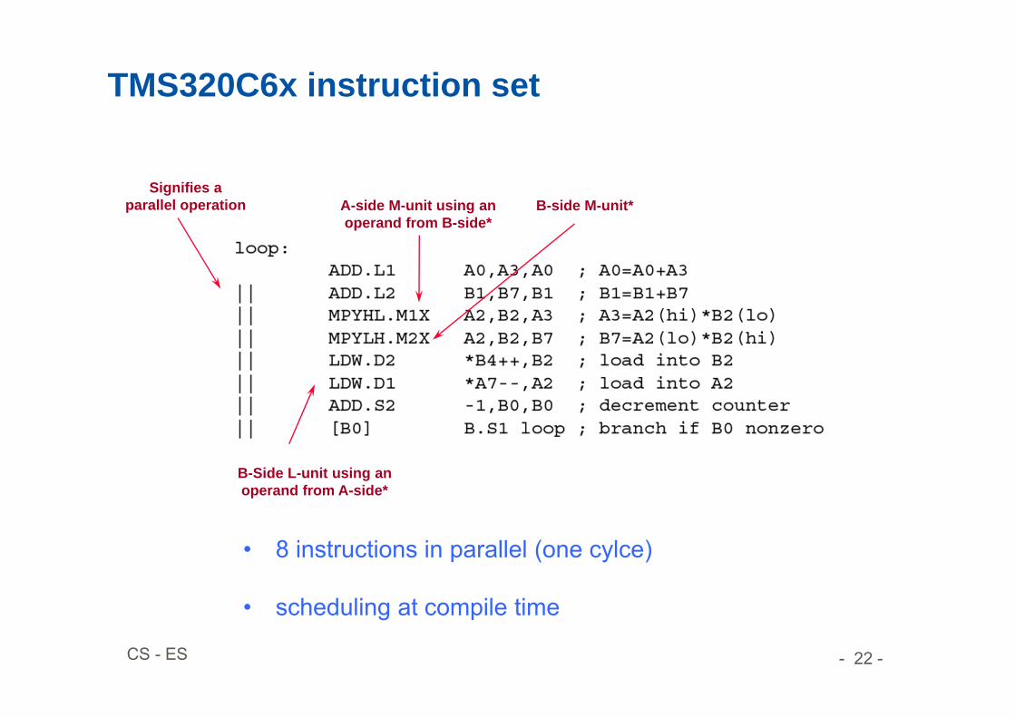
TMS320C6x instruction set
B-Side L-unit using an operand from A-side*
Signifies a parallel operation A-side M-unit using an
operand from B-side*B-side M-unit*
• 8 instructions in parallel (one cylce)
• scheduling at compile time
- 23 -CS - ES
Embedded System Hardware- Reconfigurable Hardware -
- 24 -CS - ES
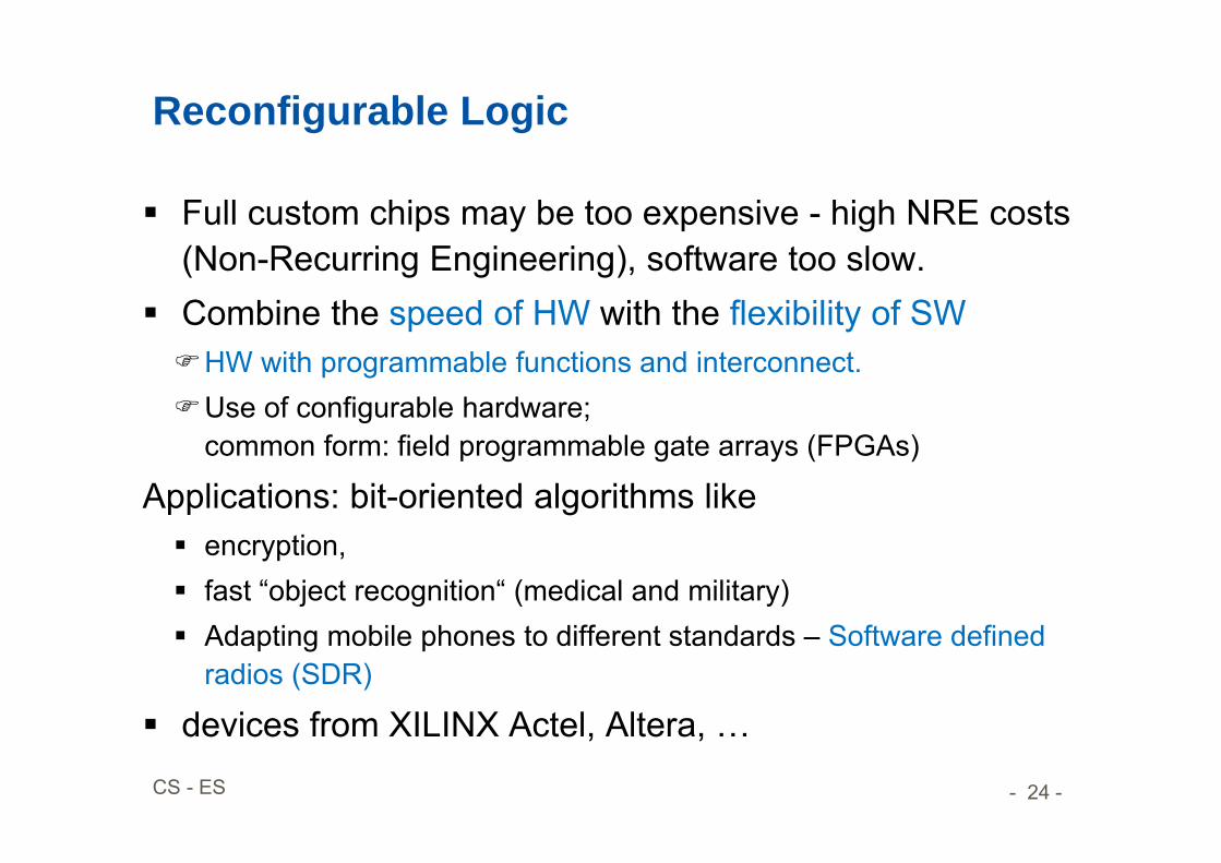
Reconfigurable Logic
Full custom chips may be too expensive - high NRE costs (Non-Recurring Engineering), software too slow.
Combine the speed of HW with the flexibility of SWHW with programmable functions and interconnect.Use of configurable hardware;
common form: field programmable gate arrays (FPGAs)
Applications: bit-oriented algorithms like encryption, fast “object recognition“ (medical and military) Adapting mobile phones to different standards – Software defined
radios (SDR)
devices from XILINX Actel, Altera, …

- 25 -CS - ES
Energy Efficiency of FPGAs
© Hugo De Man, IMEC, Philips, 2007
- 26 -CS - ES
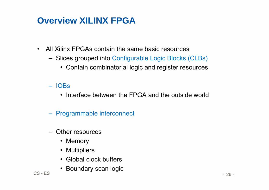
Overview XILINX FPGA
• All Xilinx FPGAs contain the same basic resources– Slices grouped into Configurable Logic Blocks (CLBs)
• Contain combinatorial logic and register resources
– IOBs• Interface between the FPGA and the outside world
– Programmable interconnect
– Other resources• Memory• Multipliers• Global clock buffers• Boundary scan logic

- 27 -CS - ES
XILINX FPGA Virtex-II Architecture
First family with Embedded Multipliers to enable high-performance DSP

- 28 -CS - ES
CLBs and Slices
Combinatorial and sequential logic implemented here
• Each Virtex-II CLB contains four slices– Local routing provides
feedback between slices in the same CLB, and it provides routing to neighboring CLBs
– A switch matrix provides access to general routing resources
CIN
SwitchMatrix
BUFTBUF T
COUTCOUT
Slice S0
Slice S1
Local Routing
Slice S2
Slice S3
CIN
SHIFT
- 29 -CS - ES
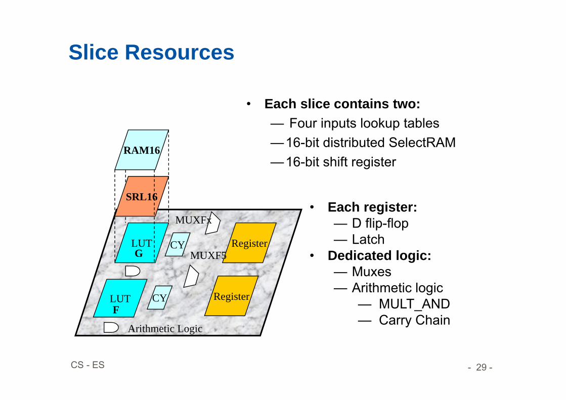
• Each slice contains two:— Four inputs lookup tables—16-bit distributed SelectRAM—16-bit shift register
• Each register:— D flip-flop— Latch
• Dedicated logic:— Muxes— Arithmetic logic
— MULT_AND— Carry Chain
LUT
Register
Register
LUT CY
CY
SRL16
RAM16
G
F
MUXF5
Arithmetic Logic
MUXFx
Slice Resources

- 30 -CS - ES
Look-Up Tables
• Combinatorial logic is stored in Look-Up Tables (LUTs) – Also called Function Generators (FGs)– Capacity is limited by the number of inputs,
not by the complexity
• Delay through the LUT is constant
Combinatorial Logic
AB
CD
Z
A B C D Z0 0 0 0 00 0 0 1 00 0 1 0 00 0 1 1 10 1 0 0 10 1 0 1 1
. . .1 1 0 0 01 1 0 1 01 1 1 0 01 1 1 1 1

- 31 -CS - ES
Routing Resources
PSM PSM
CLB
PSM PSM
CLB CLB
CLBCLB CLB
CLBCLB CLB
ProgrammableSwitchMatrix
- 32 -CS - ES
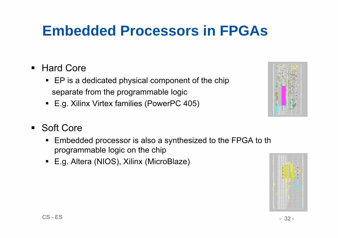
Embedded Processors in FPGAs
Hard Core EP is a dedicated physical component of the chip
separate from the programmable logic E.g. Xilinx Virtex families (PowerPC 405)
Soft Core Embedded processor is also a synthesized to the FPGA to th
programmable logic on the chip E.g. Altera (NIOS), Xilinx (MicroBlaze)
- 33 -CS - ES
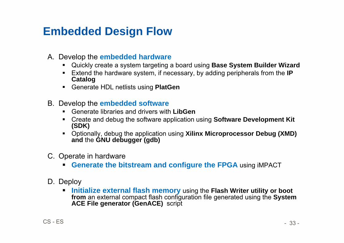
Embedded Design Flow
A. Develop the embedded hardware Quickly create a system targeting a board using Base System Builder Wizard Extend the hardware system, if necessary, by adding peripherals from the IP
Catalog Generate HDL netlists using PlatGen
B. Develop the embedded software Generate libraries and drivers with LibGen Create and debug the software application using Software Development Kit
(SDK) Optionally, debug the application using Xilinx Microprocessor Debug (XMD)
and the GNU debugger (gdb)
C. Operate in hardware Generate the bitstream and configure the FPGA using iMPACT
D. Deploy Initialize external flash memory using the Flash Writer utility or boot
from an external compact flash configuration file generated using the System ACE File generator (GenACE) script
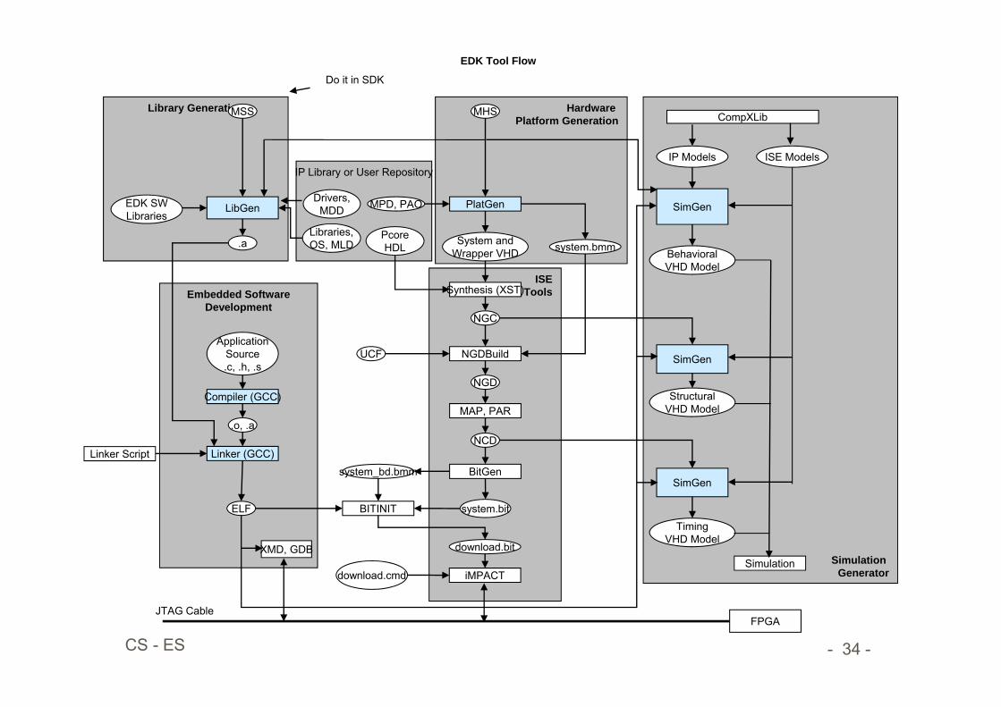
- 34 -CS - ES
Simulation Generator
Hardware Platform Generation
Library Generation
Embedded SoftwareDevelopment
ISETools
IP Library or User Repository
MSS
LibGen
.a
Compiler (GCC)
.o, .a
Linker (GCC)
ELF
MHS
PlatGenDrivers,MDD MPD, PAO
PcoreHDL System and
Wrapper VHD system.bmm
Synthesis (XST)
NGC
NGDBuildUCF
NGD
MAP, PAR
NCD
BitGensystem_bd.bmm
BITINIT
download.bit
iMPACT
system.bit
SimGen
BehavioralVHD Model
SimGen
StructuralVHD Model
SimGen
TimingVHD Model
Simulation
IP Models ISE Models
CompXLib
ApplicationSource.c, .h, .s
EDK Tool Flow
download.cmd
EDK SWLibraries
Libraries,OS, MLD
XMD, GDB
FPGAJTAG Cable
Linker Script
Do it in SDK
- 35 -CS - ES
Configuration Port or ICAP
Configuration Port
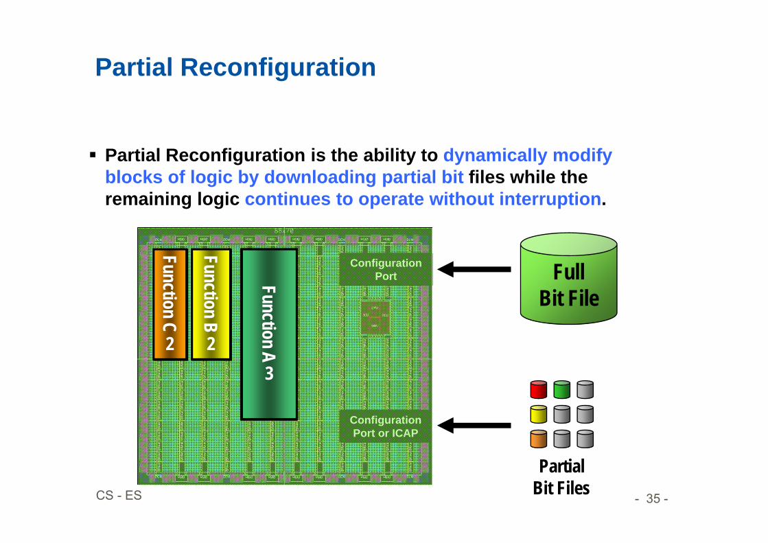
Partial Reconfiguration
FullBit File
PartialBit Files
Partial Reconfiguration is the ability to dynamically modify blocks of logic by downloading partial bit files while the remaining logic continues to operate without interruption.
Function A
1
Function B
1
Function C
1
Function C
2
Function B
2
Function A
2
Function A
3

- 36 -CS - ES
Partial Reconfiguration Technology and Benefits
Partial Reconfiguration enables: System Flexibility
• Perform more functions while maintaining communication links
Size and Cost Reduction• Time-multiplex the hardware
to require a smaller FPGA
Power Reduction• Shut down power-hungry tasks
when not needed
- 37 -CS - ES
Use Case - Simulation Platform for UHF RFID
Rapid Prototyping with FPGAs

- 38 -CS - ES
Ultra High Frequency – Radio Frequency IDentification systems
Tag design ASIC design
Communication Energy UHF field distortions
Setup
Reader designs Antenna designs
- 39 -CS - ES
Motivation Evaluate and optimize application setups
Reduced installation time Reduced on site evaluation time Proof of user requirements Worst case scenarios evaluation
Next generation protocol and product development
Verification of designs by real-time simulation of models in target setups
Offline simulations of large tag populations
Evaluation of options by simulating models

- 40 -CS - ES
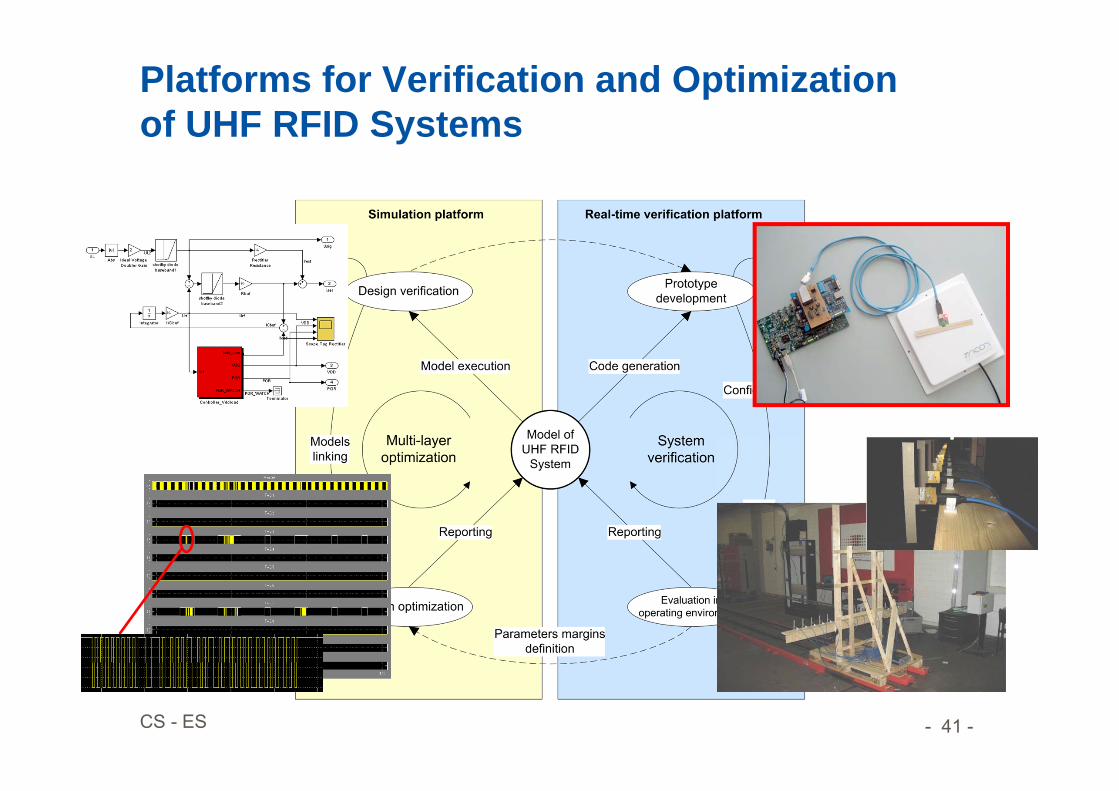
A New Framework for Real-time Verification and Optimization of UHF RFID Systems
- 41 -CS - ES
Platforms for Verification and Optimization of UHF RFID Systems
- 42 -CS - ES
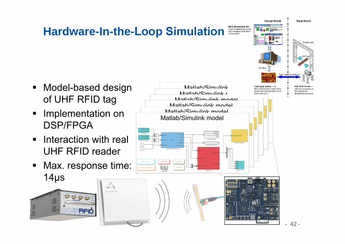
Hardware-In-the-Loop Simulation
Model-based design of UHF RFID tag
Implementation on DSP/FPGA
Interaction with real UHF RFID reader
Max. response time: 14μs
- 43 -CS - ES
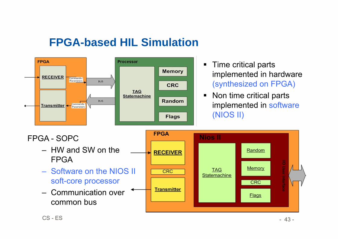
FPGA-based HIL Simulation
Time critical parts implemented in hardware (synthesized on FPGA)
Non time critical parts implemented in software(NIOS II)
FPGA - SOPC– HW and SW on the
FPGA– Software on the NIOS II
soft-core processor– Communication over
common bus
- 44 -CS - ES
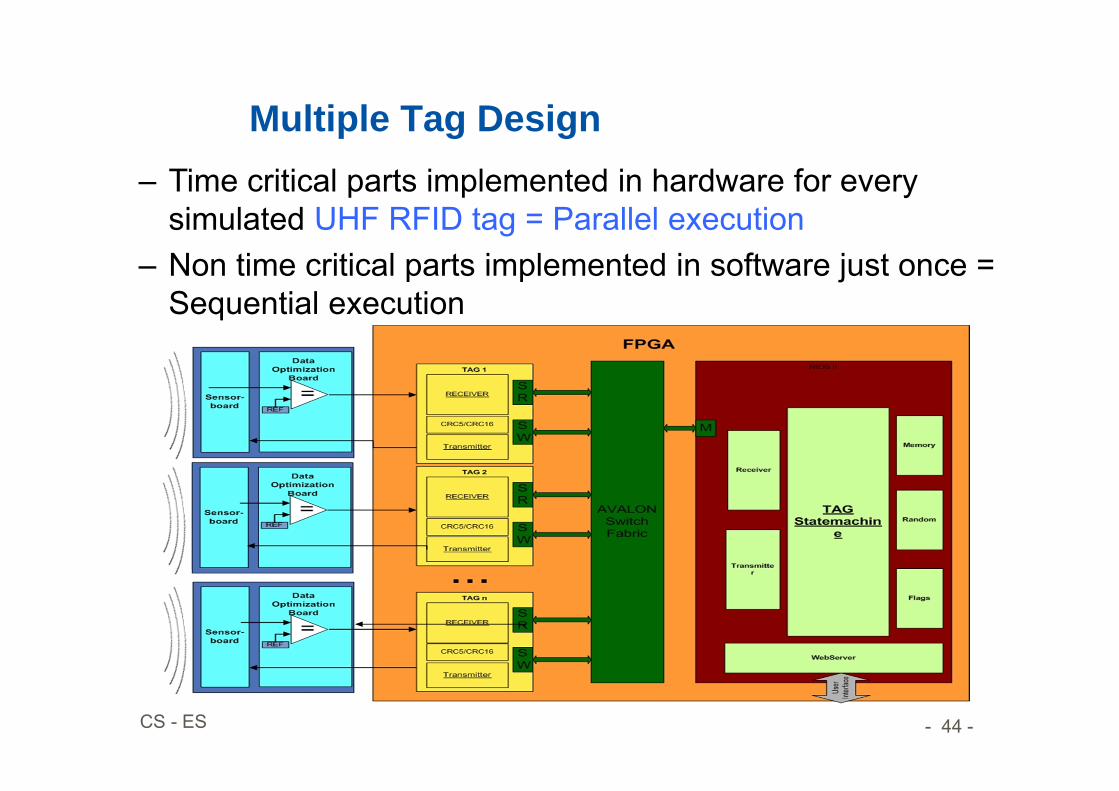
Multiple Tag Design– Time critical parts implemented in hardware for every
simulated UHF RFID tag = Parallel execution– Non time critical parts implemented in software just once =
Sequential execution
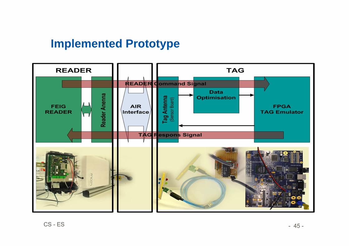
- 45 -CS - ES
Implemented Prototype
- 46 -CS - ES
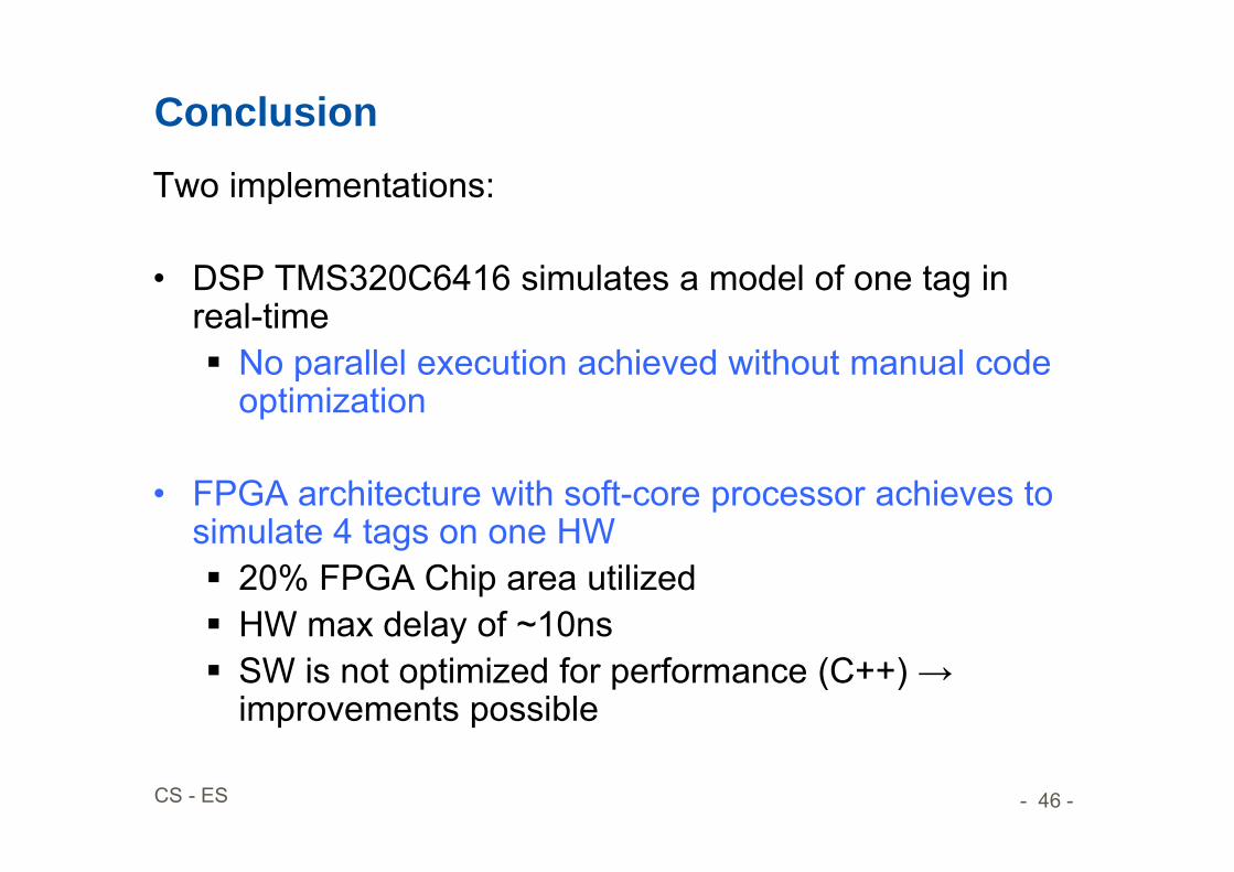
ConclusionTwo implementations:
• DSP TMS320C6416 simulates a model of one tag in real-time No parallel execution achieved without manual code
optimization
• FPGA architecture with soft-core processor achieves to simulate 4 tags on one HW 20% FPGA Chip area utilized HW max delay of ~10ns SW is not optimized for performance (C++) →
improvements possible
- 47 -CS - ES
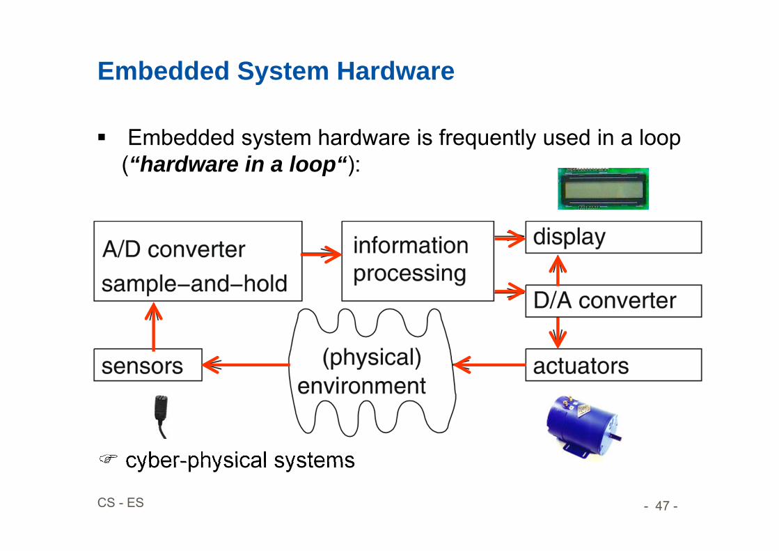
Embedded System Hardware
Embedded system hardware is frequently used in a loop(“hardware in a loop“):
cyber-physical systems
- 48 -CS - ES
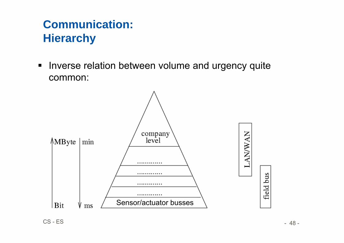
Communication:Hierarchy
Inverse relation between volume and urgency quite common:
Sensor/actuator busses
- 49 -CS - ES
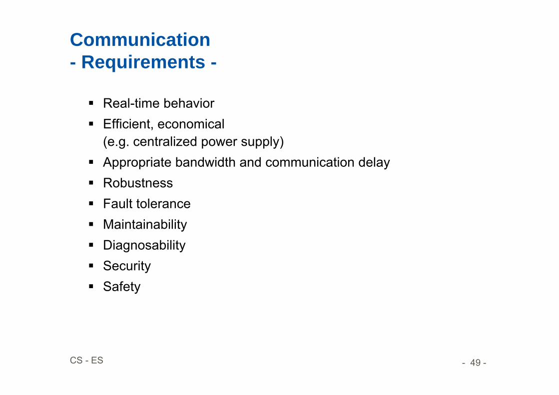
Communication- Requirements -
Real-time behavior Efficient, economical
(e.g. centralized power supply) Appropriate bandwidth and communication delay Robustness Fault tolerance Maintainability Diagnosability Security Safety
- 50 -CS - ES
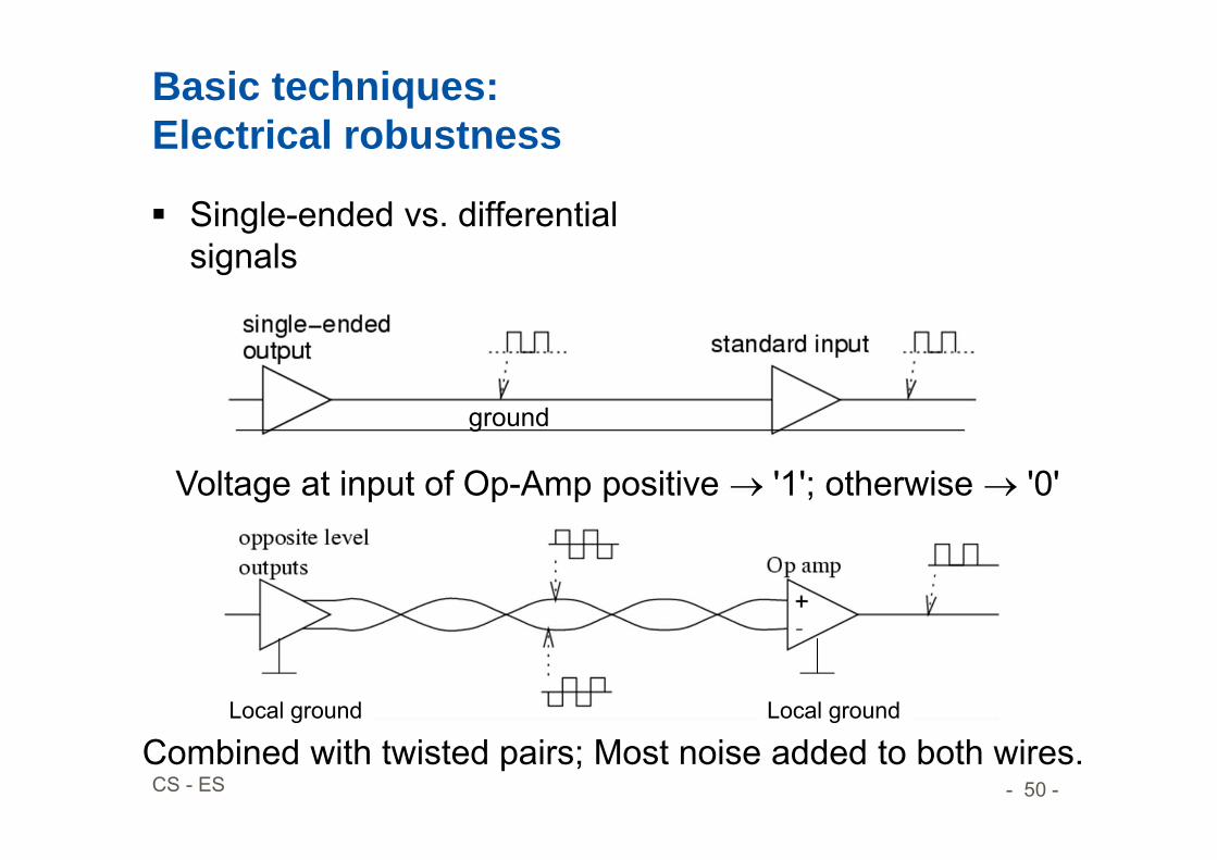
Basic techniques:Electrical robustness
Single-ended vs. differential signals
Voltage at input of Op-Amp positive '1'; otherwise '0'
Combined with twisted pairs; Most noise added to both wires.
ground
Local groundLocal ground
- 51 -CS - ES
Evaluation
Advantages: Subtraction removes most of the noise Changes of voltage levels have no effect Reduced importance of ground wiring Higher speed
Disadvantages: Requires negative voltages Increased number of wires and connectors
Applications: USB, FireWire, ISDN Ethernet (STP/UTP CAT 5/6 cables) differential SCSI High-quality analog audio signals

- 52 -CS - ES
Real-time behavior
Carrier-sense multiple-access/collision-detection (CSMA/CD, Standard Ethernet) no guaranteed response time.
Alternatives: token rings, token busses Carrier-sense multiple-access/collision-avoidance (CSMA/CA)
• WLAN techniques with request preceding transmission• Each partner gets an ID (priority). After each bus transfer, all partners
try setting their ID on the bus; partners detecting higher ID disconnect themselves from the bus. Highest priority partner gets guaranteed response time; others only if they are given a chance.
- 53 -CS - ES
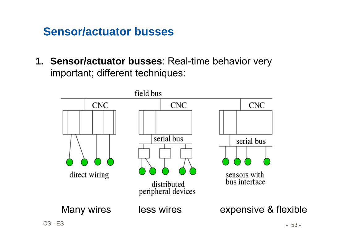
Sensor/actuator busses
1. Sensor/actuator busses: Real-time behavior very important; different techniques:
Many wires less wires expensive & flexible
- 54 -CS - ES
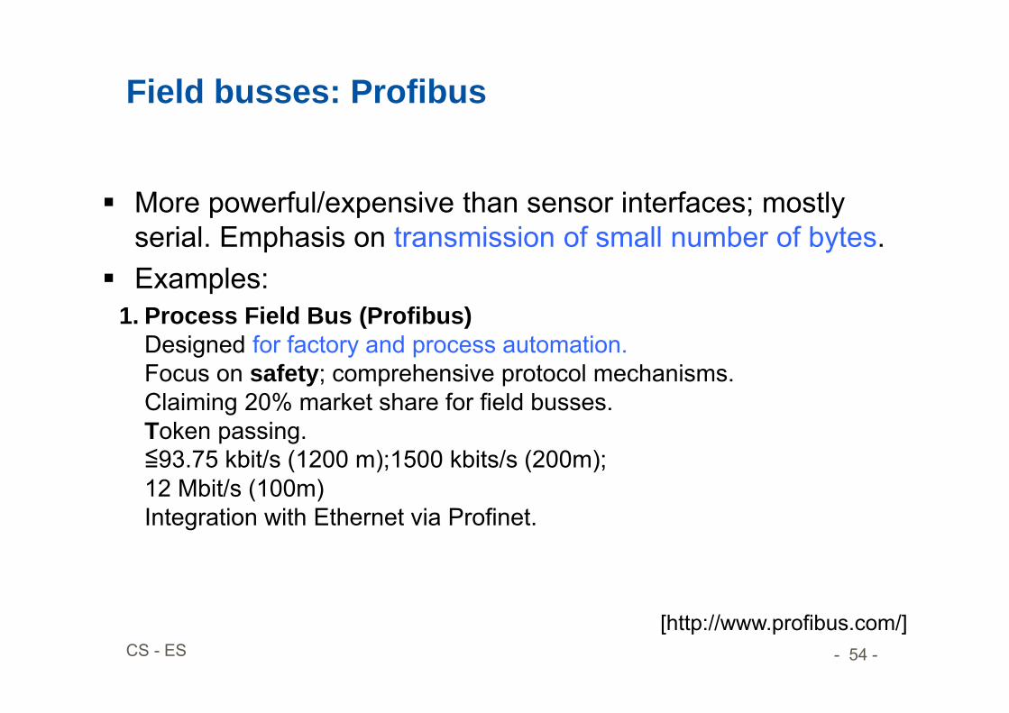
Field busses: Profibus
More powerful/expensive than sensor interfaces; mostly serial. Emphasis on transmission of small number of bytes.
Examples:1. Process Field Bus (Profibus)
Designed for factory and process automation.Focus on safety; comprehensive protocol mechanisms.Claiming 20% market share for field busses.Token passing.≦93.75 kbit/s (1200 m);1500 kbits/s (200m);12 Mbit/s (100m)Integration with Ethernet via Profinet.
[http://www.profibus.com/]
- 55 -CS - ES
Controller area network (CAN)
2. Controller area network (CAN) Designed by Bosch and Intel in 1981; used in cars and other equipment; differential signaling with twisted pairs, arbitration using CSMA/CA, throughput between 10kbit/s and 1 Mbit/s, low and high-priority signals, maximum latency of 134 µs for high priority signals, coding of signals similar to that of serial (RS-232) lines of PCs, with
modifications for differential signaling. See //www.can.bosch.com
- 56 -CS - ES
Time-Triggered-Protocol (TTP)
3. The Time-Triggered-Protocol (TTP) [Kopetz et al.]for fault-tolerant safety systems like airbags in cars.
- 57 -CS - ES
FlexRay
4. FlexRay: developed by the FlexRay consortium(BMW, Ford, Bosch, DaimlerChrysler, …)Combination of a variant of the TTP and the Byteflight [ByteflightConsortium, 2003] protocol.Specified in SDL.
• Improved error tolerance and time-determinism• Meets requirements with transfer rates >> CAN std.
High data rate can be achieved:– initially targeted for ~ 10Mbit/sec;– design allows much higher data rates
• TDMA (Time Division Multiple Access) protocol:Fixed time slot with exclusive access to the bus
• Cycle subdivided into a static and a dynamic segment.
See guest lecture from Jan. 11th. 2011
- 58 -CS - ES
Other field busses
LIN: low cost bus for interfacing sensors/actuators in the automotive domain
MOST: Multimedia bus for the automotive domain (not really a field bus)
MAP:MAP is a bus designed for car factories. EIB:The European Installation Bus (EIB) is a bus designed for
smart homes. European Installation Bus (EIB)Designed for smart buildings; CSMA/CA; low data rate.
IEEE 488: Designed for laboratory equipment.
Attempts to use standard Ethernet.However, timing predictability remains a serious issue.
- 59 -CS - ES
Wireless communication: Examples
IEEE 802.11 a/b/g/n UMTS; HSPA DECT Bluetooth ZigBee NFC
Timing predictability of wireless communication?
- 60 -CS - ES
Memory
For the memory, efficiency is again a concern: speed (latency and throughput); predictable timing energy efficiency size cost other attributes (volatile vs. persistent, etc)

- 61 -CS - ES
Memory hierarchyRegister, internalCaches in CPU
External Caches (SRAM)
Main Memory (DRAM)
Disk Storage (Magnetics)
Tape Units (Magnetics)
Ene
rgy
Con
sum
ptio
n
CO
STS
Level 0
Level 1
Level 2
Level 3
Level 4
Capacity
“Small is beautiful”(in terms of energy consumption, access times, size)
- 62 -CS - ES
The Principle of Locality
The Principle of Locality: Program access a relatively small portion of the address space
at any instant of time.
Two Different Types of Locality: Temporal Locality (Locality in Time): If an item is referenced, it
will tend to be referenced again soon (e.g., loops, reuse)
Spatial Locality (Locality in Space): If an item is referenced, items whose addresses are close by tend to be referenced soon (e.g., straightline code, array access)
- 63 -CS - ES
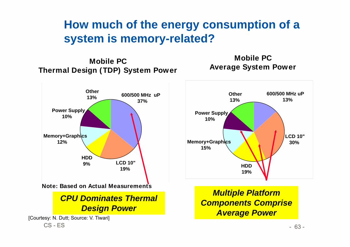
How much of the energy consumption of a system is memory-related?
Mobile PCThermal Design (TDP) System Power
Note: Based on Actual Measurements
600/500 MHz uP37%
LCD 10"19%
HDD9%
Memory+Graphics12%
Power Supply10%
Other13%
Mobile PCAverage System Power
600/500 MHz uP13%
LCD 10"30%
HDD19%
Memory+Graphics15%
Power Supply10%
Other13%
CPU Dominates Thermal Design Power
Multiple Platform Components Comprise
Average Power[Courtesy: N. Dutt; Source: V. Tiwari]

- 64 -CS - ES
Access times and energy consumption increases with the size of the memory
Example (CACTI Model): "Currently, the size of some applications is doubling every 10 months"[STMicroelectronics, Medea+ Workshop, Stuttgart, Nov. 2003]
- 65 -CS - ES
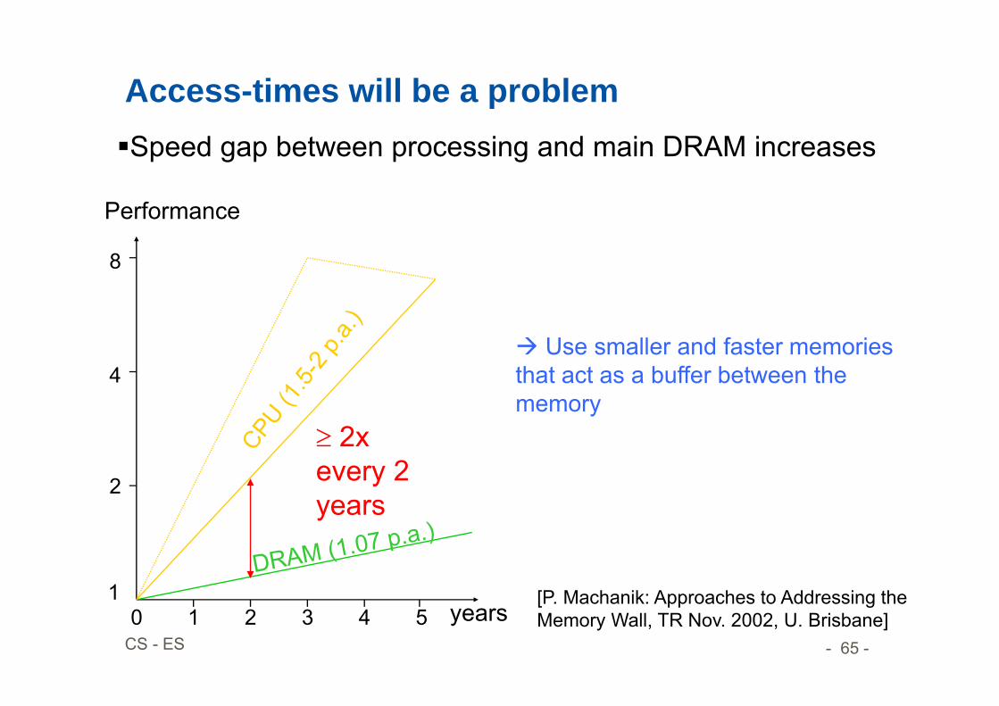
Access-times will be a problemSpeed gap between processing and main DRAM increases
2
4
8
2 4 5
Performance
years31
Use smaller and faster memories that act as a buffer between the memory
[P. Machanik: Approaches to Addressing the Memory Wall, TR Nov. 2002, U. Brisbane]
2xevery 2 years
10
- 66 -CS - ES
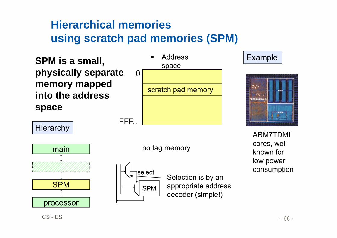
Hierarchical memoriesusing scratch pad memories (SPM)
ARM7TDMI cores, well-known for low power consumption
scratch pad memory
0
FFF..
main
SPM
processor
Hierarchy
Example
no tag memory
SPM
selectSelection is by an appropriate address decoder (simple!)
SPM is a small, physically separate memory mapped into the address space
Address space
- 67 -CS - ES
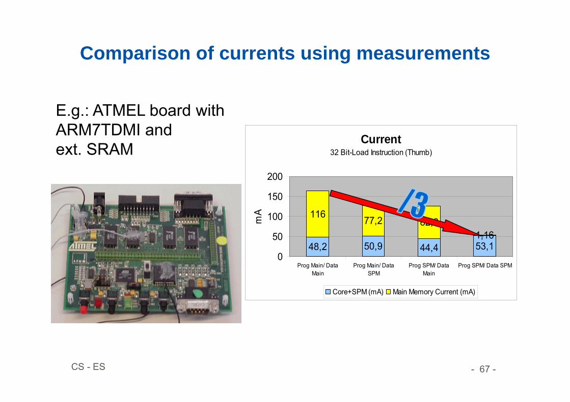
Comparison of currents using measurements
E.g.: ATMEL board with ARM7TDMI andext. SRAM
Current32 Bit-Load Instruction (Thumb)
48,2 50,9 44,4 53,1
116 77,2 82,21,16
0
50
100
150
200
Prog Main/ DataMain
Prog Main/ DataSPM
Prog SPM/ DataMain
Prog SPM/ Data SPMm
A
Core+SPM (mA) Main Memory Current (mA)
- 68 -CS - ES
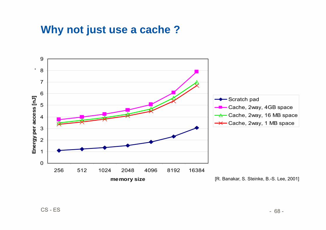
Why not just use a cache ?
0
1
2
3
4
5
6
7
8
9
256 512 1024 2048 4096 8192 16384
memory size
Ener
gy p
er a
cces
s [n
J]
.
Scratch padCache, 2way, 4GB spaceCache, 2way, 16 MB spaceCache, 2way, 1 MB space
[R. Banakar, S. Steinke, B.-S. Lee, 2001]
- 69 -CS - ES
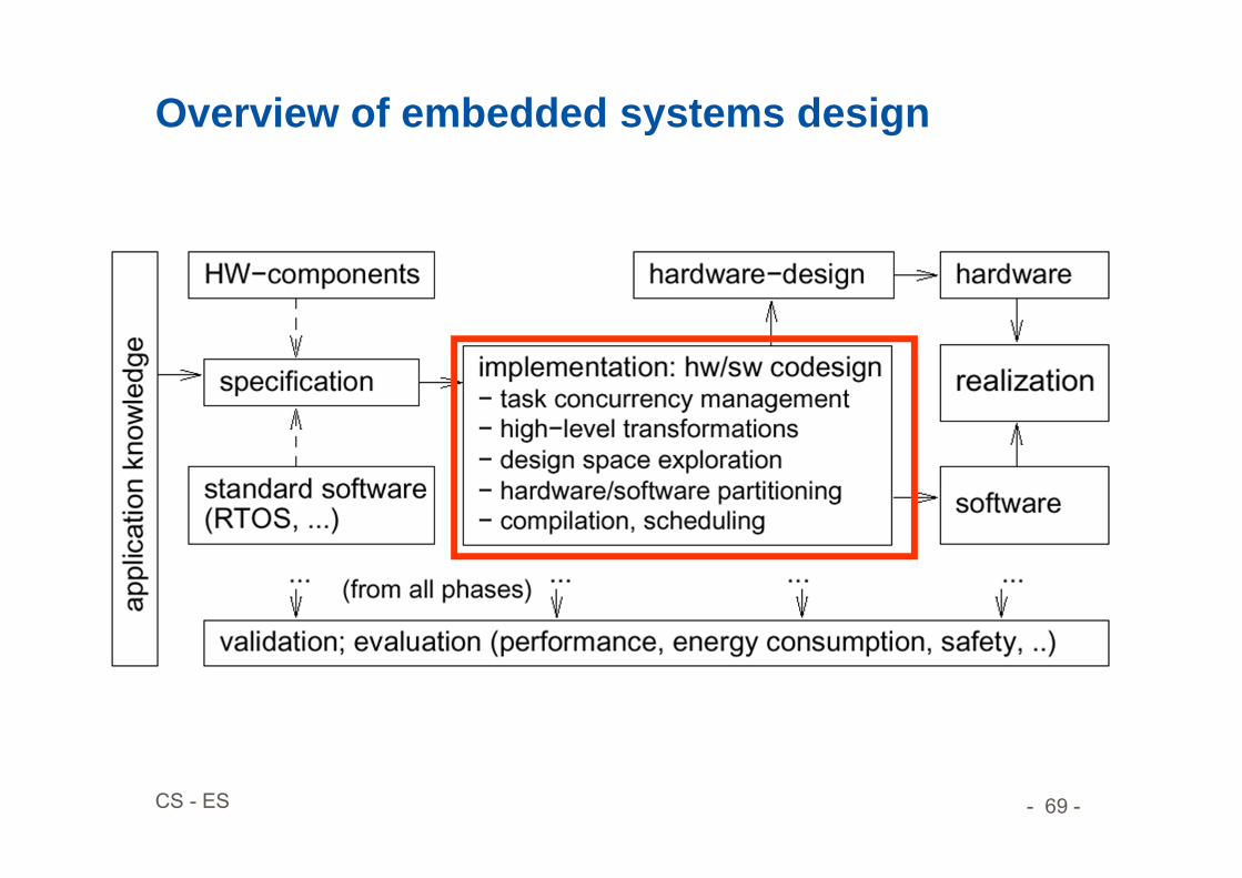
Overview of embedded systems design


![CISPA - react.uni-saarland.de · Lola Specification es Impl Monitor { # invariant = … ] while let Some(i) = get_input() { … }} Rust Code erifies MONITOR Our Goal: Verify the](https://img.pdfslide.us/doc/110x75/6031871aa2f2b6458966892d/cispa-reactuni-lola-speciication-es-impl-monitor-invariant-while-let.jpg)