Embed Size (px)
Citation preview
ELECTRICAL AND COMPUTER ENGINEERING DEPARTMENT, OAKLAND UNIVERSITY ECE-495/595: Special Topics – Reconfigurable Computing Fall 2015
1 Instructor: Daniel Llamocca
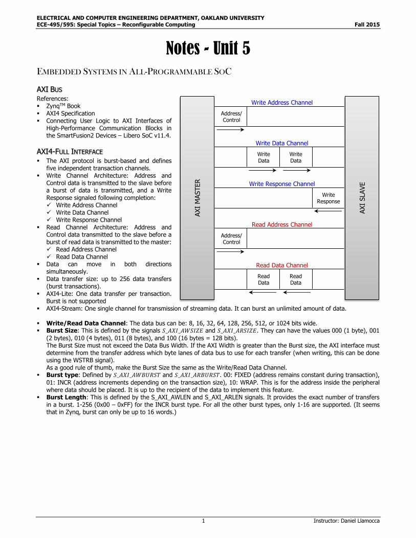
Notes - Unit 5
EMBEDDED SYSTEMS IN ALL-PROGRAMMABLE SOC
AXI BUS References: ZynqTM Book AXI4 Specification Connecting User Logic to AXI Interfaces of
High-Performance Communication Blocks in the SmartFusion2 Devices – Libero SoC v11.4.
AXI4-FULL INTERFACE
The AXI protocol is burst-based and defines five independent transaction channels.
Write Channel Architecture: Address and Control data is transmitted to the slave before a burst of data is transmitted, and a Write Response signaled following completion: Write Address Channel Write Data Channel Write Response Channel
Read Channel Architecture: Address and Control data transmitted to the slave before a burst of read data is transmitted to the master: Read Address Channel Read Data Channel
Data can move in both directions simultaneously.
Data transfer size: up to 256 data transfers (burst transactions).
AXI4-Lite: One data transfer per transaction. Burst is not supported
AXI4-Stream: One single channel for transmission of streaming data. It can burst an unlimited amount of data. Write/Read Data Channel: The data bus can be: 8, 16, 32, 64, 128, 256, 512, or 1024 bits wide. Burst Size: This is defined by the signals 𝑆_𝐴𝑋𝐼_𝐴𝑊𝑆𝐼𝑍𝐸 and 𝑆_𝐴𝑋𝐼_𝐴𝑅𝑆𝐼𝑍𝐸. They can have the values 000 (1 byte), 001
(2 bytes), 010 (4 bytes), 011 (8 bytes), and 100 (16 bytes = 128 bits). The Burst Size must not exceed the Data Bus Width. If the AXI Width is greater than the Burst size, the AXI interface must determine from the transfer address which byte lanes of data bus to use for each transfer (when writing, this can be done using the WSTRB signal). As a good rule of thumb, make the Burst Size the same as the Write/Read Data Channel.
Burst type: Defined by 𝑆_𝐴𝑋𝐼_𝐴𝑊𝐵𝑈𝑅𝑆𝑇 and 𝑆_𝐴𝑋𝐼_𝐴𝑅𝐵𝑈𝑅𝑆𝑇. 00: FIXED (address remains constant during transaction),
01: INCR (address increments depending on the transaction size), 10: WRAP. This is for the address inside the peripheral where data should be placed. It is up to the recipient of the data to implement this feature.
Burst Length: This is defined by the S_AXI_AWLEN and S_AXI_ARLEN signals. It provides the exact number of transfers in a burst. 1-256 (0x00 – 0xFF) for the INCR burst type. For all the other burst types, only 1-16 are supported. (It seems that in Zynq, burst can only be up to 16 words.)
AXI
SLAVE
AXI
MASTER
Write Address Channel
Address/Control
Write Data Channel
WriteData
WriteData
Write Response Channel
WriteResponse
Read Address Channel
Address/Control
Read Data Channel
ReadData
ReadData
ELECTRICAL AND COMPUTER ENGINEERING DEPARTMENT, OAKLAND UNIVERSITY ECE-495/595: Special Topics – Reconfigurable Computing Fall 2015
2 Instructor: Daniel Llamocca
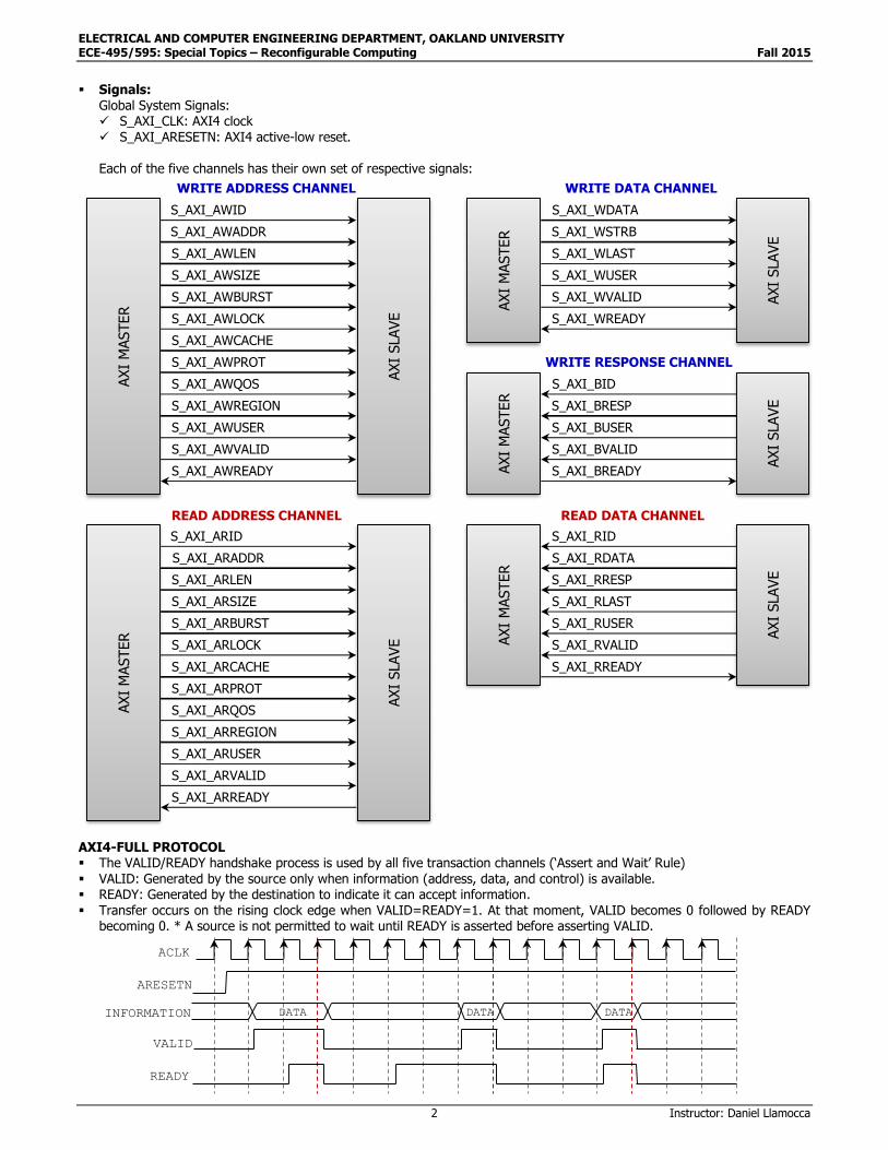
Signals: Global System Signals: S_AXI_CLK: AXI4 clock S_AXI_ARESETN: AXI4 active-low reset.
Each of the five channels has their own set of respective signals:
AXI4-FULL PROTOCOL The VALID/READY handshake process is used by all five transaction channels (‘Assert and Wait’ Rule)
VALID: Generated by the source only when information (address, data, and control) is available. READY: Generated by the destination to indicate it can accept information. Transfer occurs on the rising clock edge when VALID=READY=1. At that moment, VALID becomes 0 followed by READY
becoming 0. * A source is not permitted to wait until READY is asserted before asserting VALID.
DATA
ACLK
ARESETN
READY
VALID
INFORMATION DATA DATA
AXI
SLAVE
AXI
MASTER
WRITE ADDRESS CHANNEL
S_AXI_AWID
S_AXI_AWADDR
S_AXI_AWLEN
S_AXI_AWSIZE
S_AXI_AWBURST
S_AXI_AWLOCK
S_AXI_AWCACHE
S_AXI_AWPROT
S_AXI_AWQOS
S_AXI_AWREGION
S_AXI_AWUSER
S_AXI_AWVALID
S_AXI_AWREADY
AXI
SLAVE
AXI
MASTER
WRITE DATA CHANNEL
S_AXI_WDATA
S_AXI_WSTRB
S_AXI_WLAST
S_AXI_WUSER
S_AXI_WVALID
S_AXI_WREADY
AXI
SLAVE
AXI
MASTER
WRITE RESPONSE CHANNEL
S_AXI_BID
S_AXI_BRESP
S_AXI_BUSER
S_AXI_BVALID
S_AXI_BREADY
AXI
SLAVE
AXI
MASTER
READ ADDRESS CHANNEL
S_AXI_ARID
S_AXI_ARADDR
S_AXI_ARLEN
S_AXI_ARSIZE
S_AXI_ARBURST
S_AXI_ARLOCK
S_AXI_ARCACHE
S_AXI_ARPROT
S_AXI_ARQOS
S_AXI_ARREGION
S_AXI_ARUSER
S_AXI_ARVALID
S_AXI_ARREADY
AXI
SLAVE
AXI
MASTER
READ DATA CHANNEL
S_AXI_RDATA
S_AXI_RRESP
S_AXI_RLAST
S_AXI_RUSER
S_AXI_RVALID
S_AXI_RREADY
S_AXI_RID
ELECTRICAL AND COMPUTER ENGINEERING DEPARTMENT, OAKLAND UNIVERSITY ECE-495/595: Special Topics – Reconfigurable Computing Fall 2015
3 Instructor: Daniel Llamocca
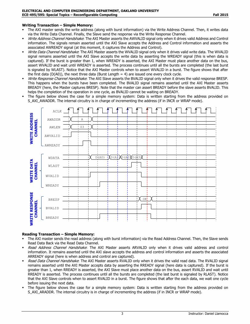
Writing Transaction – Simple Memory: The AXI master sends the write address (along with burst information) via the Write Address Channel. Then, it writes data
via the Write Data Channel. Finally, the Slave send the response via the Write Response Channel. Write Address Channel Handshake: The AXI Master asserts the AWVALID signal only when it drives valid Address and Control
information. The signals remain asserted until the AXI Slave accepts the Address and Control information and asserts the associated AWREADY signal (at this moment, it captures the Address and Control).
Write Data Channel Handshake: The AXI Master asserts the WVALID signal only when it drives valid write data. The WVALID signal remains asserted until the AXI Slave accepts the write data by asserting the WREADY signal (this is when data is captured). If the burst is greater than 1, when WREADY is asserted, the AXI Master must place another data on the bus, assert WVALID and wait until WREADY is asserted. The process continues until all the bursts are completed (the last burst is signaled by WLAST). Notice that the AXI Master controls when to assert WVALID in a burst. The figure shows that after the first data (D(A0)), the next three data (Burst Length = 4) are issued one every clock cycle.
Write Response Channel Handshake: The AXI Slave asserts the BVALID signal only when it drives the valid response BRESP. This happens when the bursts have been completed. The BVALID signal remains asserted until the AXI Master asserts BREADY (here, the Master captures BRESP). Note that the master can assert BREADY before the slave asserts BVALID. This helps the completion of the operation in one cycle, as BVALID cannot be waiting on BREADY.
The figure below shows the case for a simple memory system: Data is written starting from the address provided on S_AXI_AWADDR. The internal circuitry is in charge of incrementing the address (if in INCR or WRAP mode).
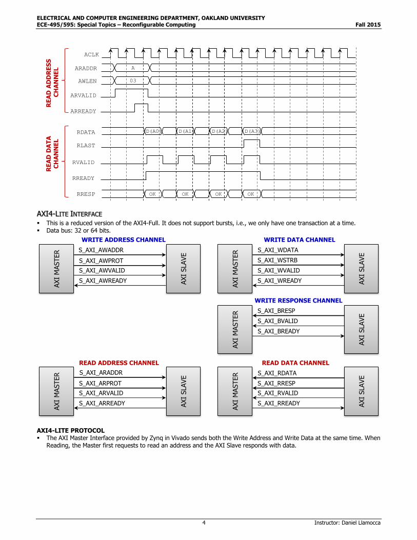
Reading Transaction – Simple Memory: The AXI master sends the read address (along with burst information) via the Read Address Channel. Then, the Slave sends
Read Data Back via the Read Data Channel.
Read Address Channel Handshake: The AXI Master asserts ARVALID only when it drives valid address and control information. It remains asserted until the AXI slave accepts the address and control information and asserts the associated ARREADY signal (here is when address and control are captured).
Read Data Channel Handshake: The AXI Master asserts RVALID only when it drives the valid read data. The RVALID signal remains asserted until the AXI Master accepts data by asserting the RREADY signal (here data is captured). If the burst is greater than 1, when RREADY is asserted, the AXI Slave must place another data on the bus, assert RVALID and wait until RREADY is asserted. The process continues until all the bursts are completed (the last burst is signaled by RLAST). Notice that the AXI Slave controls when to assert RVALID in a burst. The figure shows that after the each data, we wait one cycle before issuing the next data.
The figure below shows the case for a simple memory system: Data is written starting from the address provided on S_AXI_ARADDR. The internal circuitry is in charge of incrementing the address (if in INCR or WRAP mode).
D(A3)
ACLK
AWVALID
AWADDR A
AWREADY
WDATA
AWLEN 03
D(A0) D(A1) D(A2)
WLAST
WVALID
WREADY
OKBRESP
BVALID
BREADY
WR
ITE
AD
DR
ES
S
CH
AN
NE
LW
RIT
E D
AT
AC
HA
NN
EL
WR
ITE
RE
SP
ON
SE
CH
AN
NE
L
ELECTRICAL AND COMPUTER ENGINEERING DEPARTMENT, OAKLAND UNIVERSITY ECE-495/595: Special Topics – Reconfigurable Computing Fall 2015
4 Instructor: Daniel Llamocca
AXI4-LITE INTERFACE
This is a reduced version of the AXI4-Full. It does not support bursts, i.e., we only have one transaction at a time. Data bus: 32 or 64 bits.
AXI4-LITE PROTOCOL The AXI Master Interface provided by Zynq in Vivado sends both the Write Address and Write Data at the same time. When
Reading, the Master first requests to read an address and the AXI Slave responds with data.
D(A3)D(A1)
ACLK
ARVALID
ARADDR A
ARREADY
RDATA
AWLEN 03
D(A0)
RLAST
RVALID
RREADY
RRESP
RE
AD
AD
DR
ES
S
CH
AN
NE
LR
EA
D D
AT
AC
HA
NN
EL
D(A2)
OKOKOK OK
AXI
SLAVE
AXI
MASTER
WRITE ADDRESS CHANNEL
S_AXI_AWADDR
S_AXI_AWPROT
S_AXI_AWVALID
S_AXI_AWREADY AXI
SLAVE
AXI
MASTER
WRITE DATA CHANNEL
S_AXI_WDATA
S_AXI_WSTRB
S_AXI_WVALID
S_AXI_WREADY
AXI
SLAVE
AXI
MASTER
WRITE RESPONSE CHANNEL
S_AXI_BRESP
S_AXI_BVALID
S_AXI_BREADY
AXI
SLAVE
AXI
MASTER
READ ADDRESS CHANNEL
S_AXI_ARADDR
S_AXI_ARPROT
S_AXI_ARVALID
S_AXI_ARREADY AXI
SLAVE
AXI
MASTER
READ DATA CHANNEL
S_AXI_RDATA
S_AXI_RRESP
S_AXI_RVALID
S_AXI_RREADY
ELECTRICAL AND COMPUTER ENGINEERING DEPARTMENT, OAKLAND UNIVERSITY ECE-495/595: Special Topics – Reconfigurable Computing Fall 2015
5 Instructor: Daniel Llamocca
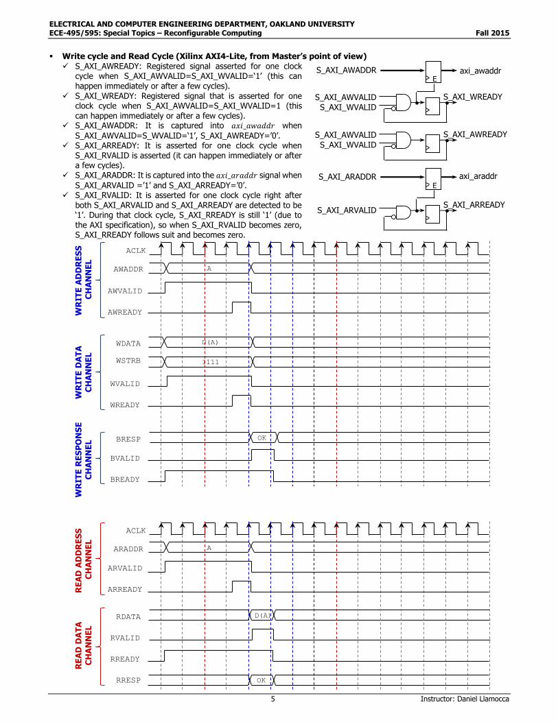
Write cycle and Read Cycle (Xilinx AXI4-Lite, from Master’s point of view) S_AXI_AWREADY: Registered signal asserted for one clock
cycle when S_AXI_AWVALID=S_AXI_WVALID=‘1’ (this can happen immediately or after a few cycles).
S_AXI_WREADY: Registered signal that is asserted for one clock cycle when S_AXI_AWVALID=S_AXI_WVALID=1 (this can happen immediately or after a few cycles).
S_AXI_AWADDR: It is captured into 𝑎𝑥𝑖_𝑎𝑤𝑎𝑑𝑑𝑟 when
S_AXI_AWVALID=S_WVALID=‘1’, S_AXI_AWREADY=’0’. S_AXI_ARREADY: It is asserted for one clock cycle when
S_AXI_RVALID is asserted (it can happen immediately or after a few cycles).
S_AXI_ARADDR: It is captured into the 𝑎𝑥𝑖_𝑎𝑟𝑎𝑑𝑑𝑟 signal when
S_AXI_ARVALID =’1’ and S_AXI_ARREADY=’0’. S_AXI_RVALID: It is asserted for one clock cycle right after
both S_AXI_ARVALID and S_AXI_ARREADY are detected to be ‘1’. During that clock cycle, S_AXI_RREADY is still ‘1’ (due to the AXI specification), so when S_AXI_RVALID becomes zero, S_AXI_RREADY follows suit and becomes zero.
D(A)
ACLK
AWVALID
AWADDR A
AWREADY
WDATA D(A)
WVALID
WREADY
OKBRESP
BVALID
BREADY
WR
ITE
AD
DR
ES
S
CH
AN
NE
LW
RIT
E D
AT
AC
HA
NN
EL
WR
ITE
RE
SP
ON
SE
CH
AN
NE
L
ACLK
ARVALID
ARADDR
ARREADY
RDATA
RVALID
RREADY
RRESP
RE
AD
AD
DR
ES
S
CH
AN
NE
LR
EA
D D
AT
AC
HA
NN
EL
OK
1111WSTRB
A
S_AXI_AWREADYS_AXI_AWVALIDS_AXI_WVALID
S_AXI_WREADYS_AXI_AWVALIDS_AXI_WVALID
axi_awaddrS_AXI_AWADDRE
S_AXI_ARREADYS_AXI_ARVALID
axi_araddrS_AXI_ARADDRE
ELECTRICAL AND COMPUTER ENGINEERING DEPARTMENT, OAKLAND UNIVERSITY ECE-495/595: Special Topics – Reconfigurable Computing Fall 2015
6 Instructor: Daniel Llamocca
AXI4 INTERFACE - EXAMPLES
AXI4-Lite Interface (Slave): Vivado 2015.3 provides a template based on the number of Slave Registers that the user specifies (4 by default). The template on its own can be used to write data on Slave Registers and read data from them in order to verify the functioning of the embedded system. In our case example, we have to modify the template to include our hardware.
AXI4-Full Interface (Slave): Vivado 2015.3 provides a template based on the number of bytes selected (64 by default). The template is a 64-bytes memory where we can read and write data using bursts. We need to modify this circuit by including our hardware.
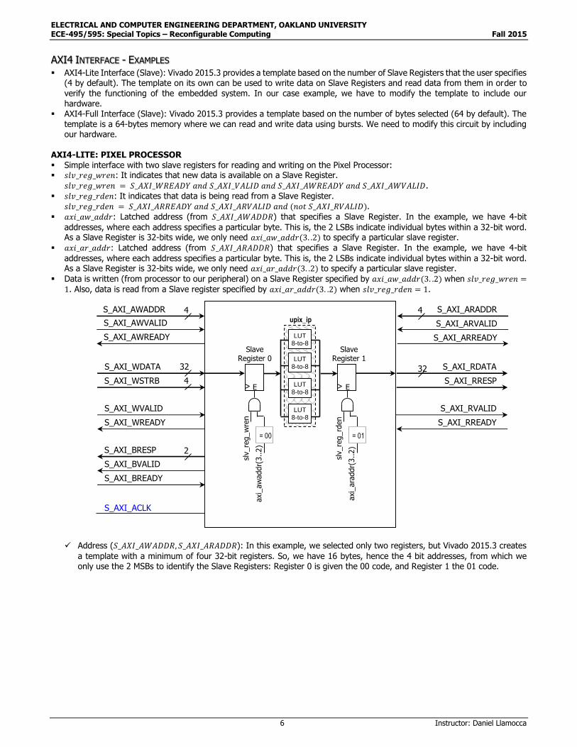
AXI4-LITE: PIXEL PROCESSOR Simple interface with two slave registers for reading and writing on the Pixel Processor: 𝑠𝑙𝑣_𝑟𝑒𝑔_𝑤𝑟𝑒𝑛: It indicates that new data is available on a Slave Register.
𝑠𝑙𝑣_𝑟𝑒𝑔_𝑤𝑟𝑒𝑛 = 𝑆_𝐴𝑋𝐼_𝑊𝑅𝐸𝐴𝐷𝑌 𝑎𝑛𝑑 𝑆_𝐴𝑋𝐼_𝑉𝐴𝐿𝐼𝐷 𝑎𝑛𝑑 𝑆_𝐴𝑋𝐼_𝐴𝑊𝑅𝐸𝐴𝐷𝑌 𝑎𝑛𝑑 𝑆_𝐴𝑋𝐼_𝐴𝑊𝑉𝐴𝐿𝐼𝐷.
𝑠𝑙𝑣_𝑟𝑒𝑔_𝑟𝑑𝑒𝑛: It indicates that data is being read from a Slave Register. 𝑠𝑙𝑣_𝑟𝑒𝑔_𝑟𝑑𝑒𝑛 = 𝑆_𝐴𝑋𝐼_𝐴𝑅𝑅𝐸𝐴𝐷𝑌 𝑎𝑛𝑑 𝑆_𝐴𝑋𝐼_𝐴𝑅𝑉𝐴𝐿𝐼𝐷 𝑎𝑛𝑑 (𝑛𝑜𝑡 𝑆_𝐴𝑋𝐼_𝑅𝑉𝐴𝐿𝐼𝐷).
𝑎𝑥𝑖_𝑎𝑤_𝑎𝑑𝑑𝑟: Latched address (from 𝑆_𝐴𝑋𝐼_𝐴𝑊𝐴𝐷𝐷𝑅) that specifies a Slave Register. In the example, we have 4-bit
addresses, where each address specifies a particular byte. This is, the 2 LSBs indicate individual bytes within a 32-bit word. As a Slave Register is 32-bits wide, we only need 𝑎𝑥𝑖_𝑎𝑤_𝑎𝑑𝑑𝑟(3. .2) to specify a particular slave register.
𝑎𝑥𝑖_𝑎𝑟_𝑎𝑑𝑑𝑟: Latched address (from 𝑆_𝐴𝑋𝐼_𝐴𝑅𝐴𝐷𝐷𝑅) that specifies a Slave Register. In the example, we have 4-bit
addresses, where each address specifies a particular byte. This is, the 2 LSBs indicate individual bytes within a 32-bit word. As a Slave Register is 32-bits wide, we only need 𝑎𝑥𝑖_𝑎𝑟_𝑎𝑑𝑑𝑟(3. .2) to specify a particular slave register.
Data is written (from processor to our peripheral) on a Slave Register specified by 𝑎𝑥𝑖_𝑎𝑤_𝑎𝑑𝑑𝑟(3. .2) when 𝑠𝑙𝑣_𝑟𝑒𝑔_𝑤𝑟𝑒𝑛 =1. Also, data is read from a Slave register specified by 𝑎𝑥𝑖_𝑎𝑟_𝑎𝑑𝑑𝑟(3. .2) when 𝑠𝑙𝑣_𝑟𝑒𝑔_𝑟𝑑𝑒𝑛 = 1.
Address (𝑆_𝐴𝑋𝐼_𝐴𝑊𝐴𝐷𝐷𝑅, 𝑆_𝐴𝑋𝐼_𝐴𝑅𝐴𝐷𝐷𝑅): In this example, we selected only two registers, but Vivado 2015.3 creates
a template with a minimum of four 32-bit registers. So, we have 16 bytes, hence the 4 bit addresses, from which we only use the 2 MSBs to identify the Slave Registers: Register 0 is given the 00 code, and Register 1 the 01 code.
= 00
LUT8-to-8
LUT8-to-8
LUT8-to-8
upix_ip
LUT8-to-8
S_AXI_AWADDR
S_AXI_AWVALID
S_AXI_AWREADY
S_AXI_WDATA
S_AXI_WSTRB
S_AXI_WVALID
S_AXI_WREADY
S_AXI_BRESP
S_AXI_BVALID
S_AXI_BREADY
4
32
4
S_AXI_ARADDR
S_AXI_ARVALID
S_AXI_ARREADY
S_AXI_RDATA
S_AXI_RRESP
S_AXI_RVALID
S_AXI_RREADY
2
4
32
S_AXI_ACLK
SlaveRegister 0
SlaveRegister 1
E E
slv_re
g_w
ren
axi_
aw
addr(
3..2)
= 01
slv_re
g_rd
en
axi_
ara
ddr(
3..2)
ELECTRICAL AND COMPUTER ENGINEERING DEPARTMENT, OAKLAND UNIVERSITY ECE-495/595: Special Topics – Reconfigurable Computing Fall 2015
7 Instructor: Daniel Llamocca
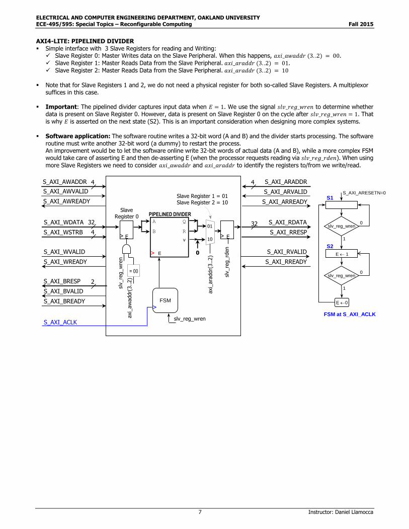
AXI4-LITE: PIPELINED DIVIDER Simple interface with 3 Slave Registers for reading and Writing:
Slave Register 0: Master Writes data on the Slave Peripheral. When this happens, 𝑎𝑥𝑖_𝑎𝑤𝑎𝑑𝑑𝑟 (3. .2) = 00.
Slave Register 1: Master Reads Data from the Slave Peripheral. 𝑎𝑥𝑖_𝑎𝑟𝑎𝑑𝑑𝑟 (3. .2) = 01.
Slave Register 2: Master Reads Data from the Slave Peripheral. 𝑎𝑥𝑖_𝑎𝑟𝑎𝑑𝑑𝑟 (3. .2) = 10
Note that for Slave Registers 1 and 2, we do not need a physical register for both so-called Slave Registers. A multiplexor
suffices in this case. Important: The pipelined divider captures input data when 𝐸 = 1. We use the signal 𝑠𝑙𝑣_𝑟𝑒𝑔_𝑤𝑟𝑒𝑛 to determine whether
data is present on Slave Register 0. However, data is present on Slave Register 0 on the cycle after 𝑠𝑙𝑣_𝑟𝑒𝑔_𝑤𝑟𝑒𝑛 = 1. That
is why 𝐸 is asserted on the next state (S2). This is an important consideration when designing more complex systems.
Software application: The software routine writes a 32-bit word (A and B) and the divider starts processing. The software
routine must write another 32-bit word (a dummy) to restart the process. An improvement would be to let the software online write 32-bit words of actual data (A and B), while a more complex FSM would take care of asserting E and then de-asserting E (when the processor requests reading via 𝑠𝑙𝑣_𝑟𝑒𝑔_𝑟𝑑𝑒𝑛). When using
more Slave Registers we need to consider 𝑎𝑥𝑖_𝑎𝑤𝑎𝑑𝑑𝑟 and 𝑎𝑥𝑖_𝑎𝑟𝑎𝑑𝑑𝑟 to identify the registers to/from we write/read.
= 00
S_AXI_AWADDR
S_AXI_AWVALID
S_AXI_AWREADY
S_AXI_WDATA
S_AXI_WSTRB
S_AXI_WVALID
S_AXI_WREADY
S_AXI_BRESP
S_AXI_BVALID
S_AXI_BREADY
4
32
4
S_AXI_ARADDR
S_AXI_ARVALID
S_AXI_ARREADY
S_AXI_RDATA
S_AXI_RRESP
S_AXI_RVALID
S_AXI_RREADY
2
4
32
S_AXI_ACLK
SlaveRegister 0
E E
slv_re
g_w
ren
axi_
aw
addr(
3..2)
slv_re
g_rd
en
axi_
ara
ddr(
3..2)
01
10
PIPELINED DIVIDER
v
E
A
B
Q
R
FSM
slv_reg_wren
0
S1
1
FSM at S_AXI_ACLK
S_AXI_ARESETN=0
slv_reg_wren
E 0
0
S2
E 1
1
slv_reg_wren0
Slave Register 1 = 01Slave Register 2 = 10
ELECTRICAL AND COMPUTER ENGINEERING DEPARTMENT, OAKLAND UNIVERSITY ECE-495/595: Special Topics – Reconfigurable Computing Fall 2015
8 Instructor: Daniel Llamocca
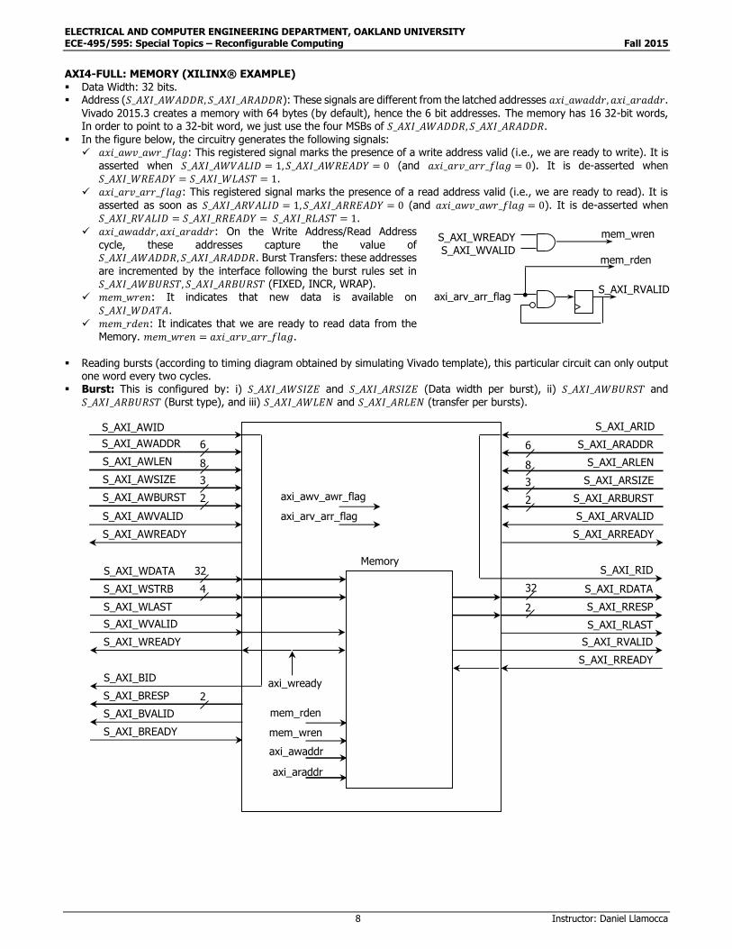
AXI4-FULL: MEMORY (XILINX® EXAMPLE) Data Width: 32 bits. Address (𝑆_𝐴𝑋𝐼_𝐴𝑊𝐴𝐷𝐷𝑅, 𝑆_𝐴𝑋𝐼_𝐴𝑅𝐴𝐷𝐷𝑅): These signals are different from the latched addresses 𝑎𝑥𝑖_𝑎𝑤𝑎𝑑𝑑𝑟, 𝑎𝑥𝑖_𝑎𝑟𝑎𝑑𝑑𝑟.
Vivado 2015.3 creates a memory with 64 bytes (by default), hence the 6 bit addresses. The memory has 16 32-bit words, In order to point to a 32-bit word, we just use the four MSBs of 𝑆_𝐴𝑋𝐼_𝐴𝑊𝐴𝐷𝐷𝑅, 𝑆_𝐴𝑋𝐼_𝐴𝑅𝐴𝐷𝐷𝑅.
In the figure below, the circuitry generates the following signals: 𝑎𝑥𝑖_𝑎𝑤𝑣_𝑎𝑤𝑟_𝑓𝑙𝑎𝑔: This registered signal marks the presence of a write address valid (i.e., we are ready to write). It is
asserted when 𝑆_𝐴𝑋𝐼_𝐴𝑊𝑉𝐴𝐿𝐼𝐷 = 1, 𝑆_𝐴𝑋𝐼_𝐴𝑊𝑅𝐸𝐴𝐷𝑌 = 0 (and 𝑎𝑥𝑖_𝑎𝑟𝑣_𝑎𝑟𝑟_𝑓𝑙𝑎𝑔 = 0). It is de-asserted when 𝑆_𝐴𝑋𝐼_𝑊𝑅𝐸𝐴𝐷𝑌 = 𝑆_𝐴𝑋𝐼_𝑊𝐿𝐴𝑆𝑇 = 1.
𝑎𝑥𝑖_𝑎𝑟𝑣_𝑎𝑟𝑟_𝑓𝑙𝑎𝑔: This registered signal marks the presence of a read address valid (i.e., we are ready to read). It is
asserted as soon as 𝑆_𝐴𝑋𝐼_𝐴𝑅𝑉𝐴𝐿𝐼𝐷 = 1, 𝑆_𝐴𝑋𝐼_𝐴𝑅𝑅𝐸𝐴𝐷𝑌 = 0 (and 𝑎𝑥𝑖_𝑎𝑤𝑣_𝑎𝑤𝑟_𝑓𝑙𝑎𝑔 = 0). It is de-asserted when 𝑆_𝐴𝑋𝐼_𝑅𝑉𝐴𝐿𝐼𝐷 = 𝑆_𝐴𝑋𝐼_𝑅𝑅𝐸𝐴𝐷𝑌 = 𝑆_𝐴𝑋𝐼_𝑅𝐿𝐴𝑆𝑇 = 1.
𝑎𝑥𝑖_𝑎𝑤𝑎𝑑𝑑𝑟, 𝑎𝑥𝑖_𝑎𝑟𝑎𝑑𝑑𝑟: On the Write Address/Read Address
cycle, these addresses capture the value of 𝑆_𝐴𝑋𝐼_𝐴𝑊𝐴𝐷𝐷𝑅, 𝑆_𝐴𝑋𝐼_𝐴𝑅𝐴𝐷𝐷𝑅. Burst Transfers: these addresses
are incremented by the interface following the burst rules set in 𝑆_𝐴𝑋𝐼_𝐴𝑊𝐵𝑈𝑅𝑆𝑇, 𝑆_𝐴𝑋𝐼_𝐴𝑅𝐵𝑈𝑅𝑆𝑇 (FIXED, INCR, WRAP).
𝑚𝑒𝑚_𝑤𝑟𝑒𝑛: It indicates that new data is available on
𝑆_𝐴𝑋𝐼_𝑊𝐷𝐴𝑇𝐴.
𝑚𝑒𝑚_𝑟𝑑𝑒𝑛: It indicates that we are ready to read data from the Memory. 𝑚𝑒𝑚_𝑤𝑟𝑒𝑛 = 𝑎𝑥𝑖_𝑎𝑟𝑣_𝑎𝑟𝑟_𝑓𝑙𝑎𝑔.
Reading bursts (according to timing diagram obtained by simulating Vivado template), this particular circuit can only output
one word every two cycles. Burst: This is configured by: i) 𝑆_𝐴𝑋𝐼_𝐴𝑊𝑆𝐼𝑍𝐸 and 𝑆_𝐴𝑋𝐼_𝐴𝑅𝑆𝐼𝑍𝐸 (Data width per burst), ii) 𝑆_𝐴𝑋𝐼_𝐴𝑊𝐵𝑈𝑅𝑆𝑇 and
𝑆_𝐴𝑋𝐼_𝐴𝑅𝐵𝑈𝑅𝑆𝑇 (Burst type), and iii) 𝑆_𝐴𝑋𝐼_𝐴𝑊𝐿𝐸𝑁 and 𝑆_𝐴𝑋𝐼_𝐴𝑅𝐿𝐸𝑁 (transfer per bursts).
S_AXI_AWID
S_AXI_AWADDR
S_AXI_AWLEN
S_AXI_AWSIZE
S_AXI_AWBURST
S_AXI_AWVALID
S_AXI_AWREADY
S_AXI_WDATA
S_AXI_WSTRB
S_AXI_WLAST
S_AXI_WVALID
S_AXI_WREADY
S_AXI_BID
S_AXI_BRESP
S_AXI_BVALID
S_AXI_BREADY
6
axi_awv_awr_flag
axi_arv_arr_flag
axi_awaddr
axi_araddr
Memory32
4
S_AXI_ARID
S_AXI_ARADDR
S_AXI_ARLEN
S_AXI_ARSIZE
S_AXI_ARBURST
S_AXI_ARVALID
S_AXI_ARREADY
S_AXI_RDATA
S_AXI_RRESP
S_AXI_RLAST
S_AXI_RVALID
S_AXI_RREADY
S_AXI_RID
8
3
2
2
6
8
3
2
32
2
mem_rden
mem_wren
axi_wready
S_AXI_RVALIDaxi_arv_arr_flag
S_AXI_WREADY
S_AXI_WVALID
mem_wren
mem_rden
ELECTRICAL AND COMPUTER ENGINEERING DEPARTMENT, OAKLAND UNIVERSITY ECE-495/595: Special Topics – Reconfigurable Computing Fall 2015
9 Instructor: Daniel Llamocca
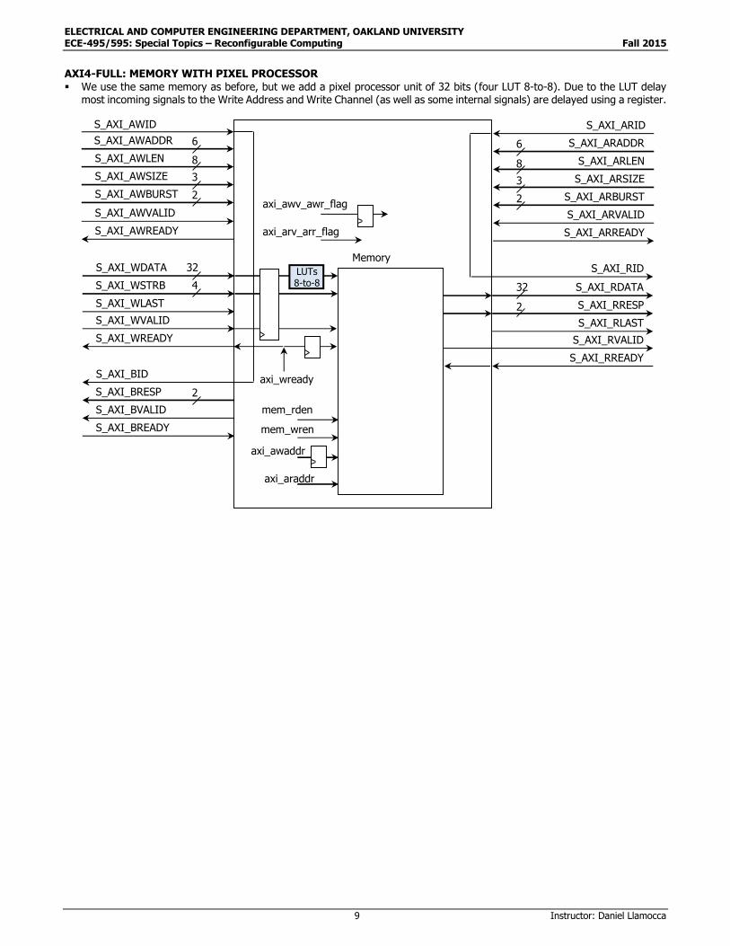
AXI4-FULL: MEMORY WITH PIXEL PROCESSOR We use the same memory as before, but we add a pixel processor unit of 32 bits (four LUT 8-to-8). Due to the LUT delay
most incoming signals to the Write Address and Write Channel (as well as some internal signals) are delayed using a register.
S_AXI_AWID
S_AXI_AWADDR
S_AXI_AWLEN
S_AXI_AWSIZE
S_AXI_AWBURST
S_AXI_AWVALID
S_AXI_AWREADY
S_AXI_WDATA
S_AXI_WSTRB
S_AXI_WLAST
S_AXI_WVALID
S_AXI_WREADY
S_AXI_BID
S_AXI_BRESP
S_AXI_BVALID
S_AXI_BREADY
6
axi_awv_awr_flag
axi_arv_arr_flag
axi_awaddr
axi_araddr
Memory32
4
S_AXI_ARID
S_AXI_ARADDR
S_AXI_ARLEN
S_AXI_ARSIZE
S_AXI_ARBURST
S_AXI_ARVALID
S_AXI_ARREADY
S_AXI_RDATA
S_AXI_RRESP
S_AXI_RLAST
S_AXI_RVALID
S_AXI_RREADY
S_AXI_RID
8
3
2
2
6
8
3
2
32
2
mem_rden
mem_wren
axi_wready
LUTs8-to-8
ELECTRICAL AND COMPUTER ENGINEERING DEPARTMENT, OAKLAND UNIVERSITY ECE-495/595: Special Topics – Reconfigurable Computing Fall 2015
10 Instructor: Daniel Llamocca
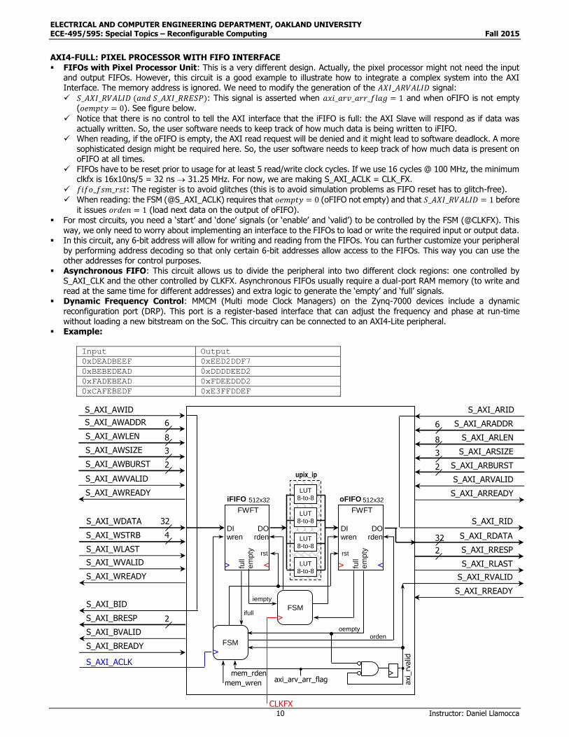
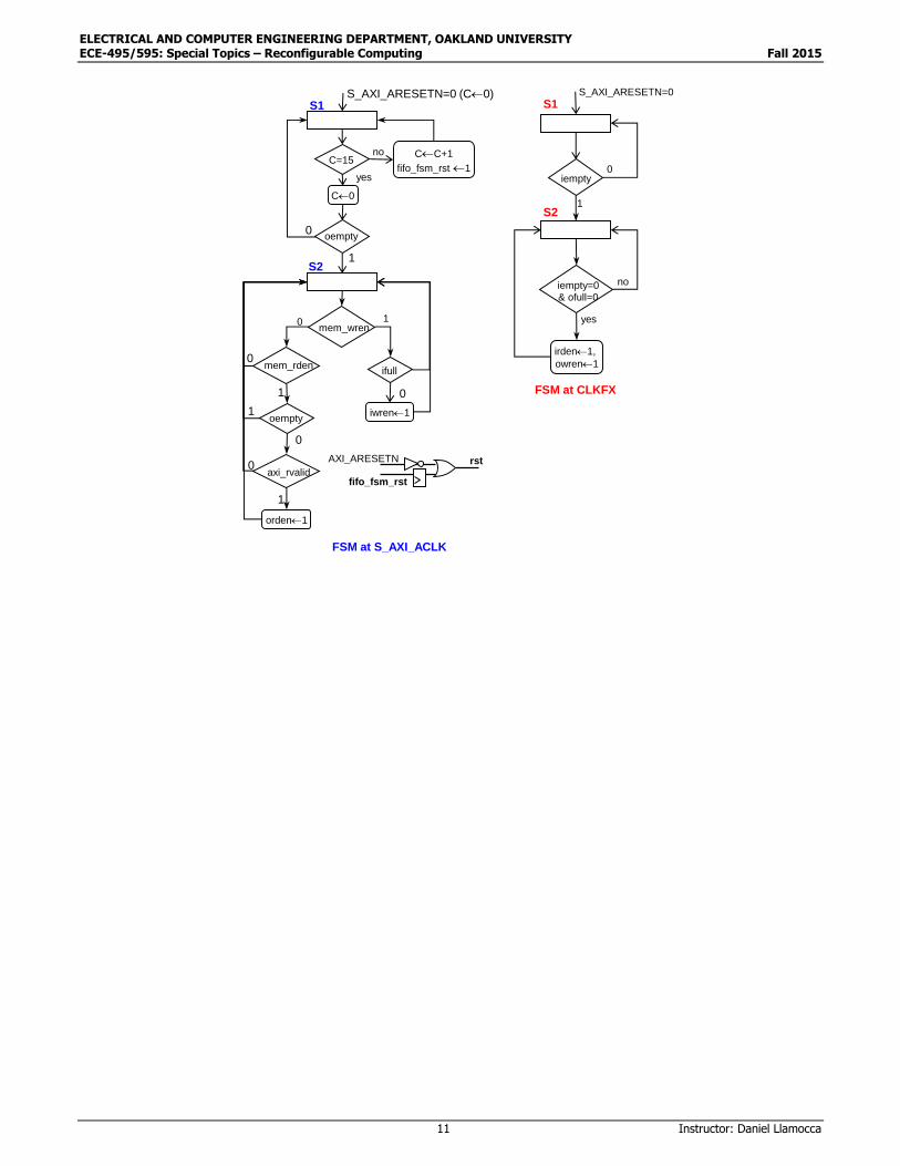
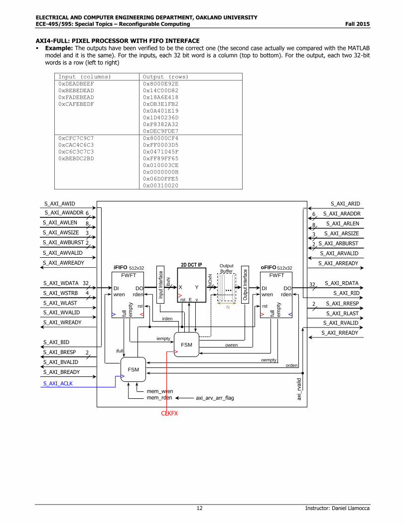
AXI4-FULL: PIXEL PROCESSOR WITH FIFO INTERFACE FIFOs with Pixel Processor Unit: This is a very different design. Actually, the pixel processor might not need the input
and output FIFOs. However, this circuit is a good example to illustrate how to integrate a complex system into the AXI Interface. The memory address is ignored. We need to modify the generation of the 𝐴𝑋𝐼_𝐴𝑅𝑉𝐴𝐿𝐼𝐷 signal:
𝑆_𝐴𝑋𝐼_𝑅𝑉𝐴𝐿𝐼𝐷 (𝑎𝑛𝑑 𝑆_𝐴𝑋𝐼_𝑅𝑅𝐸𝑆𝑃): This signal is asserted when 𝑎𝑥𝑖_𝑎𝑟𝑣_𝑎𝑟𝑟_𝑓𝑙𝑎𝑔 = 1 and when oFIFO is not empty (𝑜𝑒𝑚𝑝𝑡𝑦 = 0). See figure below.
Notice that there is no control to tell the AXI interface that the iFIFO is full: the AXI Slave will respond as if data was actually written. So, the user software needs to keep track of how much data is being written to iFIFO.
When reading, if the oFIFO is empty, the AXI read request will be denied and it might lead to software deadlock. A more sophisticated design might be required here. So, the user software needs to keep track of how much data is present on oFIFO at all times.
FIFOs have to be reset prior to usage for at least 5 read/write clock cycles. If we use 16 cycles @ 100 MHz, the minimum clkfx is 16x10ns/5 = 32 ns 31.25 MHz. For now, we are making S_AXI_ACLK = CLK_FX.
𝑓𝑖𝑓𝑜_𝑓𝑠𝑚_𝑟𝑠𝑡: The register is to avoid glitches (this is to avoid simulation problems as FIFO reset has to glitch-free).
When reading: the FSM (@S_AXI_ACLK) requires that 𝑜𝑒𝑚𝑝𝑡𝑦 = 0 (oFIFO not empty) and that 𝑆_𝐴𝑋𝐼_𝑅𝑉𝐴𝐿𝐼𝐷 = 1 before
it issues 𝑜𝑟𝑑𝑒𝑛 = 1 (load next data on the output of oFIFO).
For most circuits, you need a ‘start’ and ‘done’ signals (or ‘enable’ and ‘valid’) to be controlled by the FSM (@CLKFX). This way, we only need to worry about implementing an interface to the FIFOs to load or write the required input or output data.
In this circuit, any 6-bit address will allow for writing and reading from the FIFOs. You can further customize your peripheral by performing address decoding so that only certain 6-bit addresses allow access to the FIFOs. This way you can use the other addresses for control purposes.
Asynchronous FIFO: This circuit allows us to divide the peripheral into two different clock regions: one controlled by S_AXI_CLK and the other controlled by CLKFX. Asynchronous FIFOs usually require a dual-port RAM memory (to write and read at the same time for different addresses) and extra logic to generate the ‘empty’ and ‘full’ signals.
Dynamic Frequency Control: MMCM (Multi mode Clock Managers) on the Zynq-7000 devices include a dynamic reconfiguration port (DRP). This port is a register-based interface that can adjust the frequency and phase at run-time without loading a new bitstream on the SoC. This circuitry can be connected to an AXI4-Lite peripheral.
Example:
Input Output
0xDEADBEEF 0xEED2DDF7
0xBEBEDEAD 0xDDDDEED2
0xFADEBEAD 0xFDEEDDD2
0xCAFEBEDF 0xE3FFDDEF
S_AXI_AWID
S_AXI_AWADDR
S_AXI_AWLEN
S_AXI_AWSIZE
S_AXI_AWBURST
S_AXI_AWVALID
S_AXI_AWREADY
S_AXI_WDATA
S_AXI_WSTRB
S_AXI_WLAST
S_AXI_WVALID
S_AXI_WREADY
S_AXI_BID
S_AXI_BRESP
S_AXI_BVALID
S_AXI_BREADY
6
axi_arv_arr_flag
32
4
S_AXI_ARID
S_AXI_ARADDR
S_AXI_ARLEN
S_AXI_ARSIZE
S_AXI_ARBURST
S_AXI_ARVALID
S_AXI_ARREADY
S_AXI_RDATA
S_AXI_RRESP
S_AXI_RLAST
S_AXI_RVALID
S_AXI_RREADY
S_AXI_RID
8
3
2
2
6
8
3
2
2
32
mem_rden
axi_
rvalid
iFIFO
FWFT
DOrden
DIwren
full
em
pty
512x32
rst
FSM
LUT8-to-8
LUT8-to-8
LUT8-to-8
upix_ip
LUT8-to-8
oFIFO
FWFT
DOrden
DIwren
full
em
pty
512x32
rst
FSM
S_AXI_ACLK
CLKFX
oempty
orden
iempty
ifull
mem_wren
ELECTRICAL AND COMPUTER ENGINEERING DEPARTMENT, OAKLAND UNIVERSITY ECE-495/595: Special Topics – Reconfigurable Computing Fall 2015
11 Instructor: Daniel Llamocca
0
1 iwren1
S1
oempty
ifull
mem_wren
orden1
S2
10
01
0
1
0
oempty
FSM at S_AXI_ACLK
S_AXI_ARESETN=0 (C0)
C=15
C0
CC+1
fifo_fsm_rst 1
no
yes
rstAXI_ARESETN
fifo_fsm_rst
S1
1
FSM at CLKFX
S_AXI_ARESETN=0
iempty
irden1,
owren1
0
S2
iempty=0& ofull=0
no
yes
mem_rden
1
0axi_rvalid
ELECTRICAL AND COMPUTER ENGINEERING DEPARTMENT, OAKLAND UNIVERSITY ECE-495/595: Special Topics – Reconfigurable Computing Fall 2015
12 Instructor: Daniel Llamocca
AXI4-FULL: PIXEL PROCESSOR WITH FIFO INTERFACE Example: The outputs have been verified to be the correct one (the second case actually we compared with the MATLAB
model and it is the same). For the inputs, each 32 bit word is a column (top to bottom). For the output, each two 32-bit words is a row (left to right)
Input (columns) Output (rows)
0xDEADBEEF
0xBEBEDEAD
0xFADEBEAD
0xCAFEBEDF
0x8000E92E
0x14C00D82
0x18A6E418
0xDB3E1FB2
0x0A401E19
0x1D40236D
0xF8382A32
0xDEC9FDE7
0xCFC7C9C7
0xCAC4C6C3
0xC6C3C7C3
0xBEBDC2BD
0x80000CF4
0xFF0003D5
0x0471045F
0xFF89FF65
0x010003CE
0x0000000B
0x06D0FFE5
0x00310020
S_AXI_AWID
S_AXI_AWADDR
S_AXI_AWLEN
S_AXI_AWSIZE
S_AXI_AWBURST
S_AXI_AWVALID
S_AXI_AWREADY
S_AXI_WDATA
S_AXI_WSTRB
S_AXI_WLAST
S_AXI_WVALID
S_AXI_WREADY
S_AXI_BID
S_AXI_BRESP
S_AXI_BVALID
S_AXI_BREADY
6
axi_arv_arr_flag
32
4
S_AXI_ARID
S_AXI_ARADDR
S_AXI_ARLEN
S_AXI_ARSIZE
S_AXI_ARBURST
S_AXI_ARVALID
S_AXI_ARREADY
S_AXI_RDATA
S_AXI_RRESP
S_AXI_RLAST
S_AXI_RVALID
S_AXI_RREADY
S_AXI_RID
8
3
2
2
6
8
3
2
2
32
mem_wrenmem_rden a
xi_
rvalid
iFIFO
FWFT
DOrden
DIwren
full
em
pty
512x32
rst
FSM
oFIFO
FWFT
DOrden
DIwren
full
em
pty
512x32
rst
FSM
S_AXI_ACLK
CLKFX
oempty
orden
iempty
ifull
2D DCT IP
E v
X
Inpu
t Int
erfa
ce
rst
...
OutputBuffer
NO
xN
N
BxN
Out
put I
nter
face
Y
irden
owren