Embed Size (px)
Citation preview
EMBEDDED SYSTEM DESIGN
UNIT 1
INTRODUCTION TO EMBEDDED SYSTEM
Embedded systems overview
An embedded system is nearly any computing system other than a desktop computer. An
embedded system is a dedicated system which performs the desired function upon power up,
repeatedly.
Embedded systems are found in a variety of common electronic devices such as consumer
electronics ex. Cell phones, pagers, digital cameras, VCD players, portable Video games,
calculators, etc.,
Embedded systems are found in a variety of common electronic devices, such as:
(a)consumer electronics -- cell phones, pagers, digital cameras, camcorders, videocassette
recorders, portable video games, calculators, and personal digital assistants; (b) home appliances
-- microwave ovens, answering machines, thermostat, home security, washing machines, and
lighting systems; (c) office automation -- fax machines, copiers, printers, and scanners; (d)
business equipment -- cash registers, curbside check-in, alarm systems, card readers, product
scanners, and automated teller machines; (e) automobiles --transmission control, cruise control,
fuel injection, anti-lock brakes, and active suspension
Classifications of Embedded systems
1. Small Scale Embedded Systems: These systems are designed with a single 8- or 16-bit
microcontroller; they have little hardware and software complexities and involve board-
level design. They may even be battery operated. When developing embedded software
for these, an editor, assembler and cross assembler, specific to the microcontroller or
processor used, are the main programming tools. Usually, ‗C‘ is used for developing
these systems. ‗C‘ program compilation is done into the assembly, and executable codes
are then appropriately located in the system memory. The software has to fit within the
memory available and keep in view the need to limit power dissipation when system is
running continuously.
2. Medium Scale Embedded Systems: These systems are usually designed with a single or
few 16- or 32-bit microcontrollers or DSPs or Reduced Instruction Set Computers
(RISCs). These have both hardware and software complexities. For complex software
design, there are the following programming tools: RTOS, Source code engineering tool,
Simulator, Debugger and Integrated Development Environment (IDE). Software tools
also provide the solutions to the hardware complexities. An assembler is of little use as a
programming tool. These systems may also employ the readily available ASSPs and IPs
(explained later) for the various functions—for example, for the bus interfacing,
encrypting, deciphering, discrete cosine transformation and inverse transformation,
TCP/IP protocol stacking and network connecting functions.
3. Sophisticated Embedded Systems: Sophisticated embedded systems have enormous
hardware and software complexities and may need scalable processors or configurable
processors and programmable logic arrays. They are used for cutting edge applications
that need hardware and software co-design and integration in the final system; however,
they are constrained by the processing speeds available in their hardware units. Certain
software functions such as encryption and deciphering algorithms, discrete cosine
transformation and inverse transformation algorithms, TCP/IP protocol stacking and
network driver functions are implemented in the hardware to obtain additional speeds by
saving time. Some of the functions of the hardware resources in the system are also
implemented by the software. Development tools for these systems may not be readily
available at a reasonable cost or may not be available at all. In some cases, a compiler or
retarget able compiler might have to be developed for these.
The processing units of the embedded system
1. Processor in an Embedded System A processor is an important unit in the embedded
system hardware. A microcontroller is an integrated chip that has the processor, memory
and several other hardware units in it; these form the microcomputer part of the
embedded system. An embedded processor is a processor with special features that allow
it to be embedded into a system. A digital signal processor (DSP) is a processor meant for
applications that process digital signals.
2. Commonly used microprocessors, microcontrollers and DSPs in the small-, medium-and
large scale embedded systems
3. A recently introduced technology that additionally incorporates the application-specific
system processors (ASSPs) in the embedded systems.
4. Multiple processors in a system.
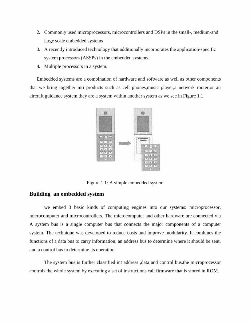
Embedded systems are a combination of hardware and software as well as other components
that we bring together inti products such as cell phones,music player,a network router,or an
aircraft guidance system.they are a system within another system as we see in Figure 1.1
Figure 1.1: A simple embedded system
Building an embedded system
we embed 3 basic kinds of computing engines into our systems: microprocessor,
microcomputer and microcontrollers. The microcomputer and other hardware are connected via
A system bus is a single computer bus that connects the major components of a computer
system. The technique was developed to reduce costs and improve modularity. It combines the
functions of a data bus to carry information, an address bus to determine where it should be sent,
and a control bus to determine its operation.
The system bus is further classified int address ,data and control bus.the microprocessor
controls the whole system by executing a set of instructions call firmware that is stored in ROM.
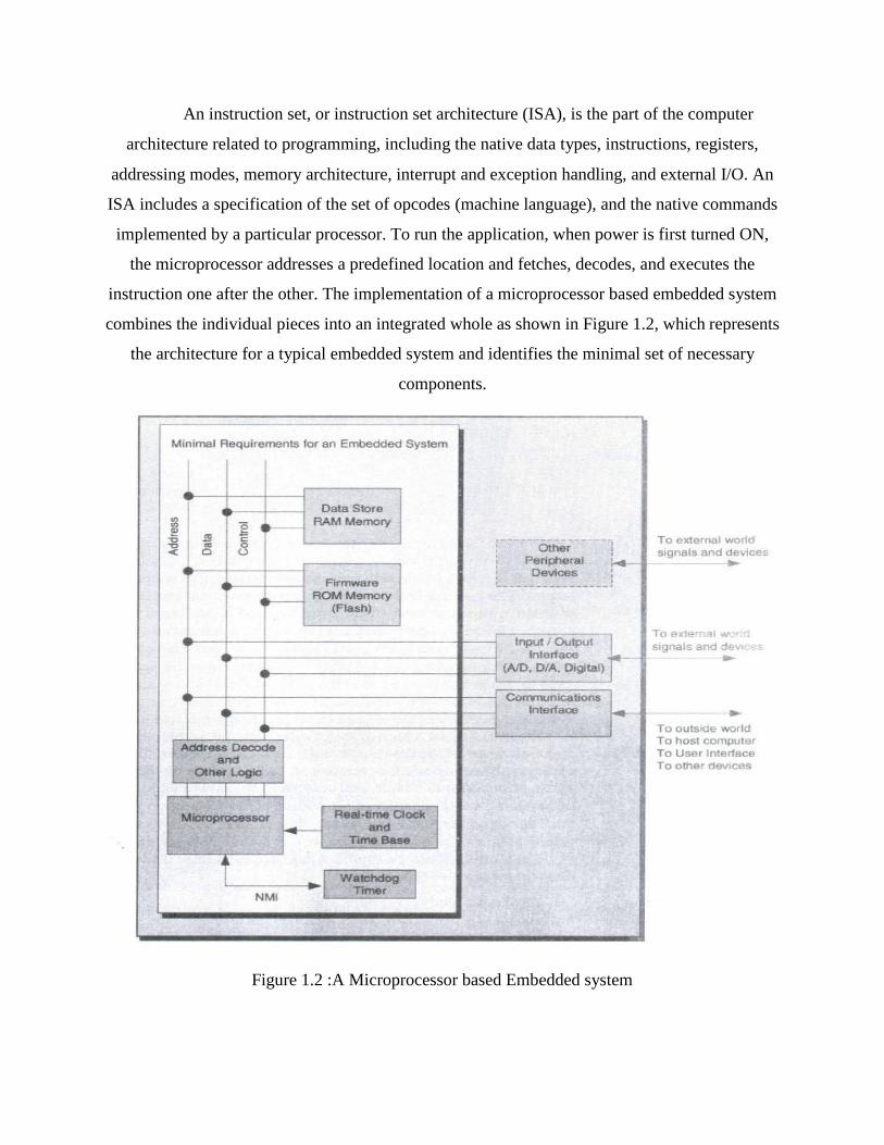
An instruction set, or instruction set architecture (ISA), is the part of the computer
architecture related to programming, including the native data types, instructions, registers,
addressing modes, memory architecture, interrupt and exception handling, and external I/O. An
ISA includes a specification of the set of opcodes (machine language), and the native commands
implemented by a particular processor. To run the application, when power is first turned ON,
the microprocessor addresses a predefined location and fetches, decodes, and executes the
instruction one after the other. The implementation of a microprocessor based embedded system
combines the individual pieces into an integrated whole as shown in Figure 1.2, which represents
the architecture for a typical embedded system and identifies the minimal set of necessary
components.
Figure 1.2 :A Microprocessor based Embedded system
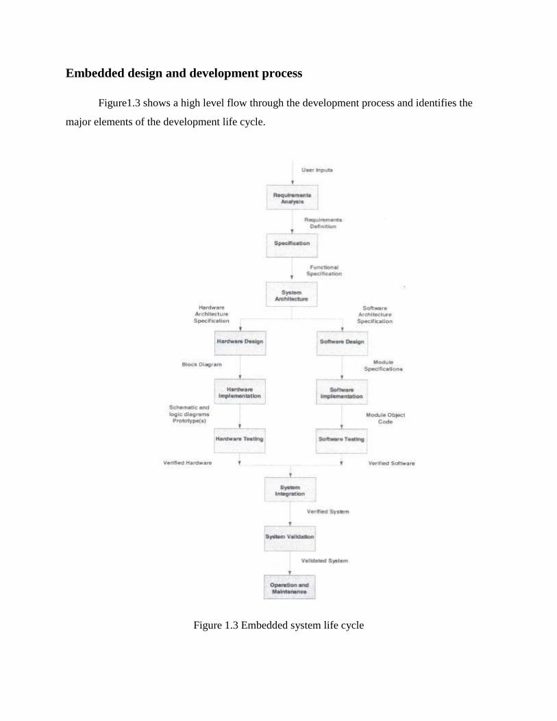
Embedded design and development process
Figure1.3 shows a high level flow through the development process and identifies the
major elements of the development life cycle.
Figure 1.3 Embedded system life cycle
The traditional design approach has been traverse the two sides of the accompanying diagram
separately, that is,
Design the hardware components
Design the software components.
Bring the two together.
Spend time testing and debugging the system.
The major areas of the design process are
Ensuring a sound software and hardware specification.
Formulating the architecture for the system to be designed.
Partitioning the h/w and s/w.
Providing an iterative approach to the design of h/w and s/w.
The important steps in developing an embedded system are
Requirement definition.
System specification.
Functional design
Architectural design
Prototyping.
The major aspects in the development of embedded applications are
Digital hardware and software architecture
Formal design , development, and optimization process.
Safety and reliability.
Digital hardware and software/firmware design.
The interface to physical world analog and digital signals.
Debug, troubleshooting and test of our design.
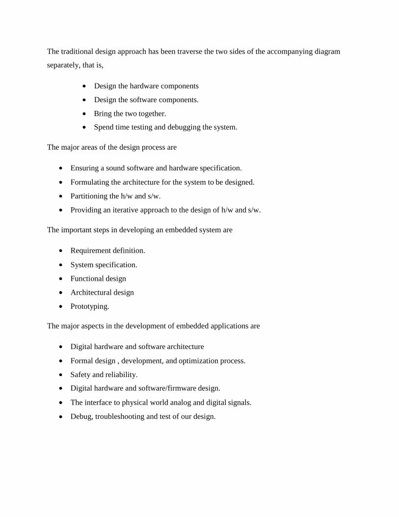
Figure 1.4: Interfacing to the outside world
Embedded applications are intended to work with the physical world, sensing various
analog and digital signals while controlling, manipulating or responding to others. The study of
the interface to the external world extends the I/O portion of the von-Neumann machine as
shown in figure 1.4 with a study of buses, their constitutes and their timing considerations.
Exemplary applications of each type of embedded system
Embedded systems have very diversified applications. A few select application areas of
embedded systems are Telecom, Smart Cards, Missiles and Satellites, Computer Networking,
Digital Consumer Electronics, and Automotive. Figure 1.9 shows the applications of embedded
systems in these areas.
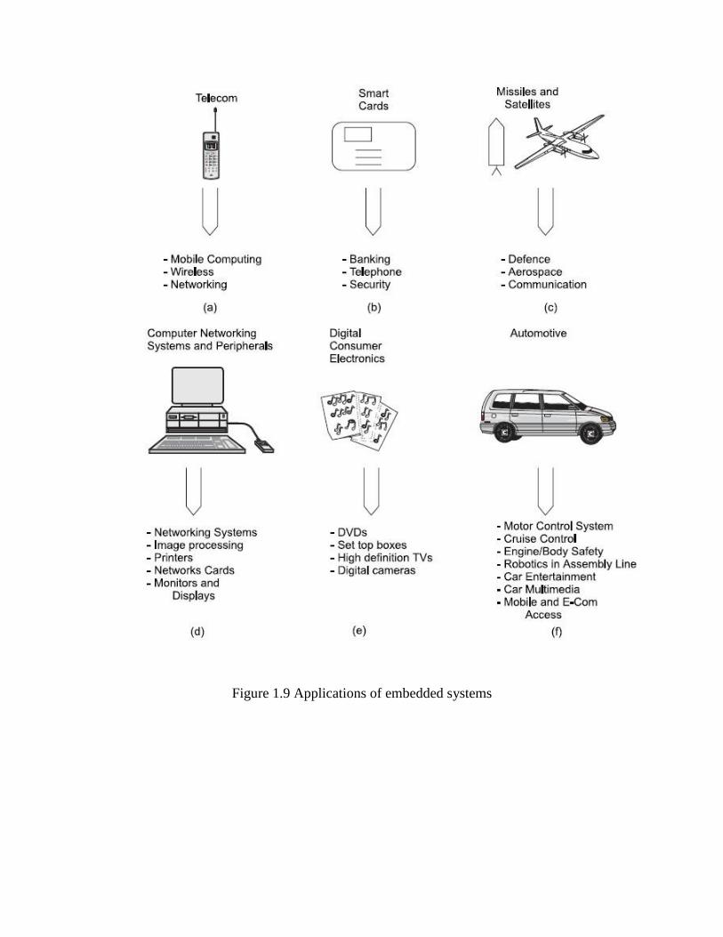
Figure 1.9 Applications of embedded systems
UNIT 2
THE HARDWARE SIDE
In today‘s hi-tech and changing world, we can put together a working hierarchy of hard
ware components. At the top, we find VLSI circuits comprising of significant pieces of
functionality: microprocessor, microcontrollers, FPGA‘s, CPLD, and ASIC.
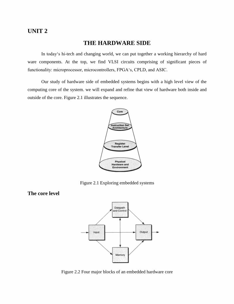
Our study of hardware side of embedded systems begins with a high level view of the
computing core of the system. we will expand and refine that view of hardware both inside and
outside of the core. Figure 2.1 illustrates the sequence.
Figure 2.1 Exploring embedded systems
The core level
Figure 2.2 Four major blocks of an embedded hardware core
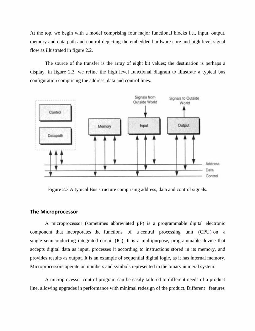
At the top, we begin with a model comprising four major functional blocks i.e., input, output,
memory and data path and control depicting the embedded hardware core and high level signal
flow as illustrated in figure 2.2.
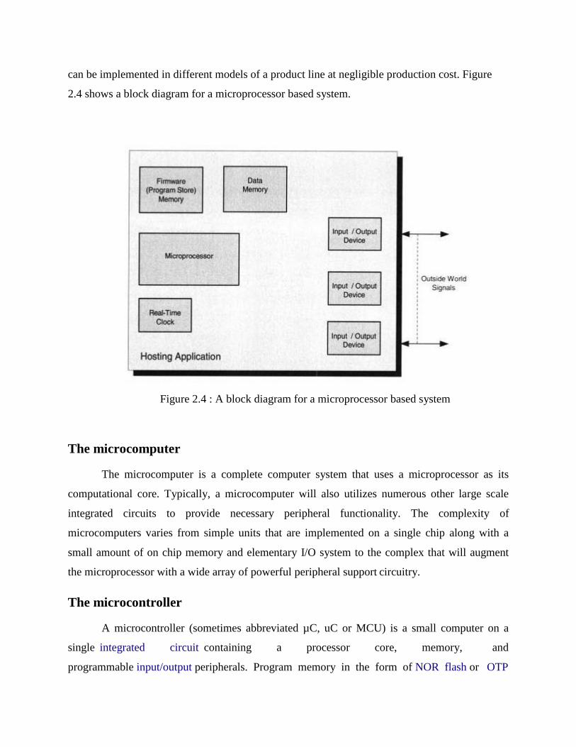
The source of the transfer is the array of eight bit values; the destination is perhaps a
display. in figure 2.3, we refine the high level functional diagram to illustrate a typical bus
configuration comprising the address, data and control lines.
Figure 2.3 A typical Bus structure comprising address, data and control signals.
The Microprocessor
A microprocessor (sometimes abbreviated µP) is a programmable digital electronic
component that incorporates the functions of a central processing unit (CPU) on a
single semiconducting integrated circuit (IC). It is a multipurpose, programmable device that
accepts digital data as input, processes it according to instructions stored in its memory, and
provides results as output. It is an example of sequential digital logic, as it has internal memory.
Microprocessors operate on numbers and symbols represented in the binary numeral system.
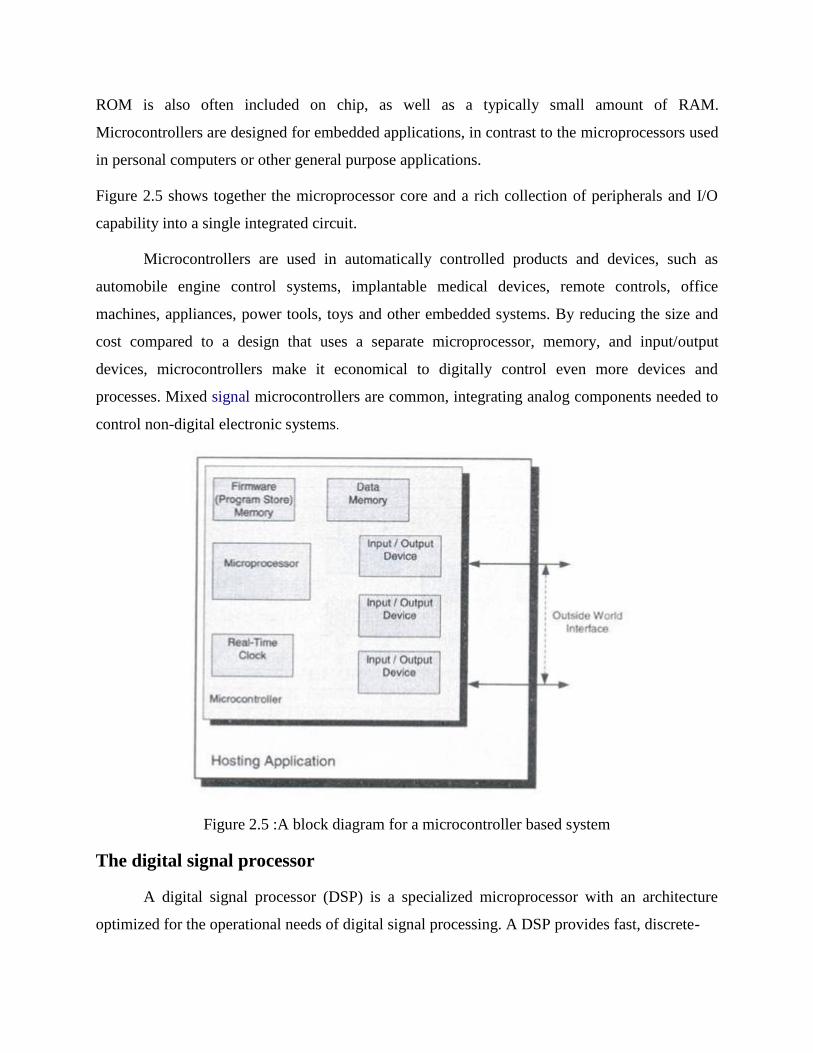
A microprocessor control program can be easily tailored to different needs of a product
line, allowing upgrades in performance with minimal redesign of the product. Different features
can be implemented in different models of a product line at negligible production cost. Figure
2.4 shows a block diagram for a microprocessor based system.
Figure 2.4 : A block diagram for a microprocessor based system
The microcomputer
The microcomputer is a complete computer system that uses a microprocessor as its
computational core. Typically, a microcomputer will also utilizes numerous other large scale
integrated circuits to provide necessary peripheral functionality. The complexity of
microcomputers varies from simple units that are implemented on a single chip along with a
small amount of on chip memory and elementary I/O system to the complex that will augment
the microprocessor with a wide array of powerful peripheral support circuitry.
The microcontroller
A microcontroller (sometimes abbreviated µC, uC or MCU) is a small computer on a
single integrated circuit containing a processor core, memory, and
programmable input/output peripherals. Program memory in the form of NOR flash or OTP
ROM is also often included on chip, as well as a typically small amount of RAM.
Microcontrollers are designed for embedded applications, in contrast to the microprocessors used
in personal computers or other general purpose applications.
Figure 2.5 shows together the microprocessor core and a rich collection of peripherals and I/O
capability into a single integrated circuit.
Microcontrollers are used in automatically controlled products and devices, such as
automobile engine control systems, implantable medical devices, remote controls, office
machines, appliances, power tools, toys and other embedded systems. By reducing the size and
cost compared to a design that uses a separate microprocessor, memory, and input/output
devices, microcontrollers make it economical to digitally control even more devices and
processes. Mixed signal microcontrollers are common, integrating analog components needed to
control non-digital electronic systems.
Figure 2.5 :A block diagram for a microcontroller based system
The digital signal processor
A digital signal processor (DSP) is a specialized microprocessor with an architecture
optimized for the operational needs of digital signal processing. A DSP provides fast, discrete-
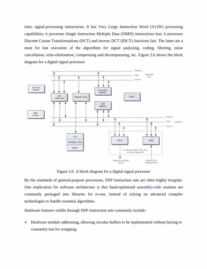
time, signal-processing instructions. It has Very Large Instruction Word (VLIW) processing
capabilities; it processes Single Instruction Multiple Data (SIMD) instructions fast; it processes
Discrete Cosine Transformations (DCT) and inverse DCT (IDCT) functions fast. The latter are a
must for fast execution of the algorithms for signal analyzing, coding, filtering, noise
cancellation, echo-elimination, compressing and decompressing, etc. Figure 2.6 shows the block
diagram for a digital signal processor
Figure 2.6 A block diagram for a digital signal processor
By the standards of general-purpose processors, DSP instruction sets are often highly irregular.
One implication for software architecture is that hand-optimized assembly-code routines are
commonly packaged into libraries for re-use, instead of relying on advanced compiler
technologies to handle essential algorithms.
Hardware features visible through DSP instruction sets commonly include:
Hardware modulo addressing, allowing circular buffers to be implemented without having to
constantly test for wrapping.
Memory architecture designed for streaming data, using DMA extensively and expecting
code to be written to know about cache hierarchies and the associated delays.
Driving multiple arithmetic units may require memory architectures to support several
accesses per instruction cycle
Separate program and data memories (Harvard architecture), and sometimes concurrent
access on multiple data busses
Special SIMD (single instruction, multiple data) operations
Some processors use VLIW techniques so each instruction drives multiple arithmetic units in
parallel
Special arithmetic operations, such as fast multiply–accumulates (MACs). Many
fundamental DSP algorithms, such as FIR filters or the Fast Fourier transform (FFT) depend
heavily on multiply–accumulate performance.
Bit-reversed addressing, a special addressing mode useful for calculating FFTs
Special loop controls, such as architectural support for executing a few instruction words in a
very tight loop without overhead for instruction fetches or exit testing
Deliberate exclusion of a memory management unit. DSPs frequently use multi-tasking
operating systems, but have no support for virtual memory or memory protection. Operating
systems that use virtual memory require more time for context switching among processes,
which increases latency.
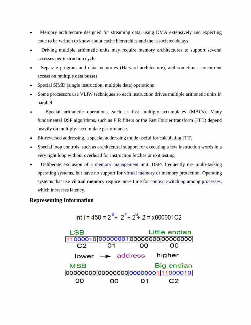
Representing Information
Big endian systems are simply those systems whose memories are organized with the
most significant digits or bytes of a number or series of numbers in the upper left corner of a
memory page and the least significant in the lower right, just as in a normal spreadsheet.
Little endian systems are simply those system whose memories are organized with the
least significant digits or bytes of a number or series of numbers in the upper left corner of a
memory page and the most significant in the lower right. There are many examples of both types
of systems, with the principle reasons for the choice of either format being the underlying
operation of the given system.
Understanding numbers
We have seen that within a microprocessor, we don‘t have an unbounded numbers of bits with
which to express the various kinds of numeric information that we will be working with in an
embedded application. The limitation of finite word size can have unintended consequences of
results of any mathematical operations that we might need to perform. Let‘s examine the effects
of finite word size on resolution, accuracy, errors and the propagation of errors in these
operation. In an embedded system, the integers and floating point numbers are normally
represented as binary values and are stored either in memory or in registers. The expensive
power of any number is dependent on the number of bits in the number.
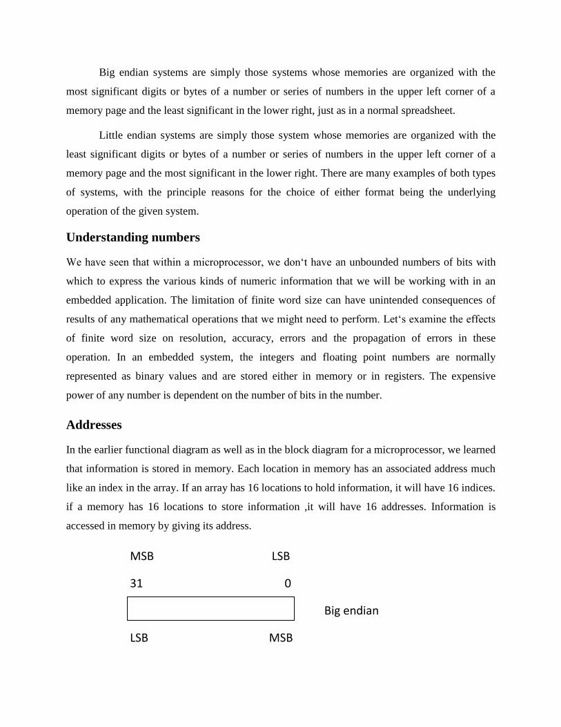
Addresses
In the earlier functional diagram as well as in the block diagram for a microprocessor, we learned
that information is stored in memory. Each location in memory has an associated address much
like an index in the array. If an array has 16 locations to hold information, it will have 16 indices.
if a memory has 16 locations to store information ,it will have 16 addresses. Information is
accessed in memory by giving its address.
MSB LSB
31 0
Big endian
LSB MSB
0 31
Little endian
Figure Expressing Addresses
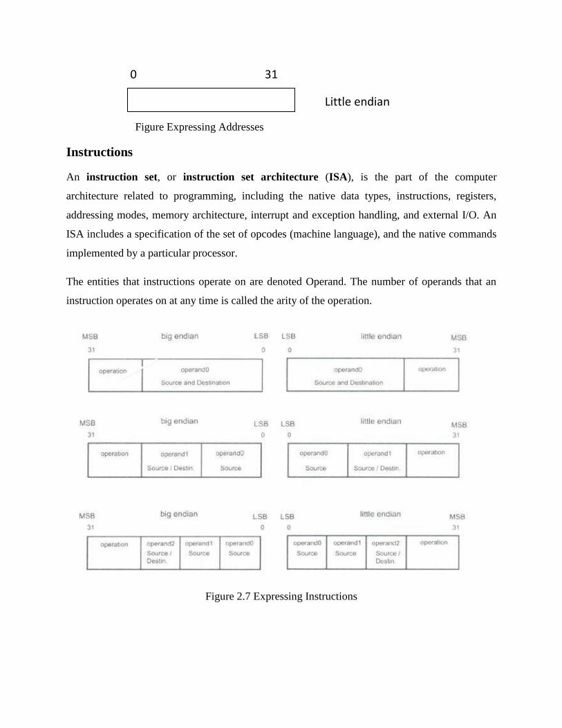
Instructions
An instruction set, or instruction set architecture (ISA), is the part of the computer
architecture related to programming, including the native data types, instructions, registers,
addressing modes, memory architecture, interrupt and exception handling, and external I/O. An
ISA includes a specification of the set of opcodes (machine language), and the native commands
implemented by a particular processor.
The entities that instructions operate on are denoted Operand. The number of operands that an
instruction operates on at any time is called the arity of the operation.
Figure 2.7 Expressing Instructions
In figure 2.7 ,we see that within the 32 bit word, the bit are aggregated into groups or fields.
Some of the fields are interpreted as the operation to be performed, and others are seen as the
operands involved in the operation.
Embedded systems-An instruction set view
A microprocessor instruction set specifies the basic operations supported by the machine. From
the earlier functional model, we see that the objectives of such operations are to transfer or store
data, to operate on data, and to make decisions based on the data values or outcome of the
operations, corresponding to such operations, we can classify instructions into the following
groups
Data transfer
Flow control
Arithmetic and logic
Data transfer Instructions
Data transfer instructions are responsible for moving data around inside the processor as well as
for bringing data in from the outside world or sending data out. The source and destination can
be any of the following:
A register
Memory
An input or output
As shown in figure
Addressing modes
There are five addressing modes in 8085.
1.Direct Addressing Mode
1. Register Addressing Mode
2. Register Indirect Addressing Mode
3. Immediate Addressing Mode
4. Implicit Addressing Mode
Direct Addressing Mode
In this mode, the address of the operand is given in the instruction itself.
LDA is the operation.
2500 H is the address of source.
Accumulator is the destination.
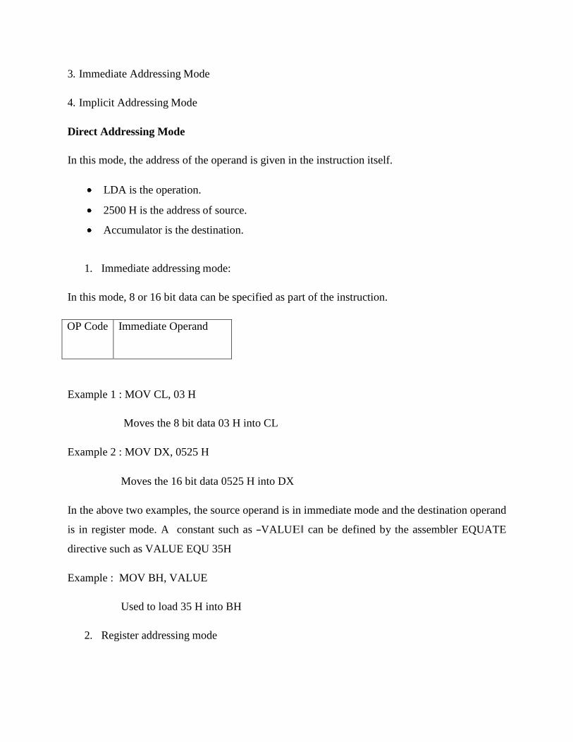
1. Immediate addressing mode:
In this mode, 8 or 16 bit data can be specified as part of the instruction.
OP Code Immediate Operand
Example 1 : MOV CL, 03 H
Moves the 8 bit data 03 H into CL
Example 2 : MOV DX, 0525 H
Moves the 16 bit data 0525 H into DX
In the above two examples, the source operand is in immediate mode and the destination operand
is in register mode. A constant such as ―VALUE‖ can be defined by the assembler EQUATE
directive such as VALUE EQU 35H
Example : MOV BH, VALUE
Used to load 35 H into BH
2. Register addressing mode
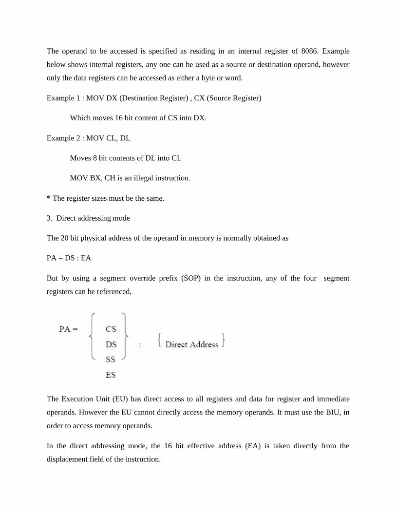
The operand to be accessed is specified as residing in an internal register of 8086. Example
below shows internal registers, any one can be used as a source or destination operand, however
only the data registers can be accessed as either a byte or word.
Example 1 : MOV DX (Destination Register) , CX (Source Register)
Which moves 16 bit content of CS into DX.
Example 2 : MOV CL, DL
Moves 8 bit contents of DL into CL
MOV BX, CH is an illegal instruction.
* The register sizes must be the same.
3. Direct addressing mode
The 20 bit physical address of the operand in memory is normally obtained as
PA = DS : EA
But by using a segment override prefix (SOP) in the instruction, any of the four segment
registers can be referenced,
The Execution Unit (EU) has direct access to all registers and data for register and immediate
operands. However the EU cannot directly access the memory operands. It must use the BIU, in
order to access memory operands.
In the direct addressing mode, the 16 bit effective address (EA) is taken directly from the
displacement field of the instruction.
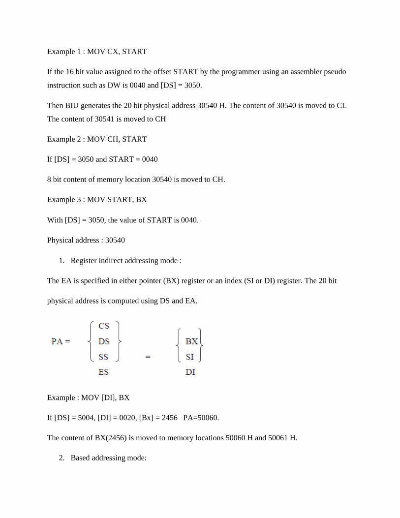
Example 1 : MOV CX, START
If the 16 bit value assigned to the offset START by the programmer using an assembler pseudo
instruction such as DW is 0040 and [DS] = 3050.
Then BIU generates the 20 bit physical address 30540 H. The content of 30540 is moved to CL
The content of 30541 is moved to CH
Example 2 : MOV CH, START
If [DS] = 3050 and START = 0040
8 bit content of memory location 30540 is moved to CH.
Example 3 : MOV START, BX
With [DS] = 3050, the value of START is 0040.
Physical address : 30540
1. Register indirect addressing mode :
The EA is specified in either pointer (BX) register or an index (SI or DI) register. The 20 bit
physical address is computed using DS and EA.
Example : MOV [DI], BX
If [DS] = 5004, [DI] = 0020, [Bx] = 2456 PA=50060.
The content of BX(2456) is moved to memory locations 50060 H and 50061 H.
2. Based addressing mode:
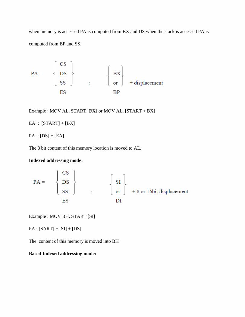
when memory is accessed PA is computed from BX and DS when the stack is accessed PA is
computed from BP and SS.
Example : MOV AL, START [BX] or MOV AL, [START + BX]
EA : [START] + [BX]
PA : [DS] + [EA]
The 8 bit content of this memory location is moved to AL.
Indexed addressing mode:
Example : MOV BH, START [SI]
PA : [SART] + [SI] + [DS]
The content of this memory is moved into BH
Based Indexed addressing mode:
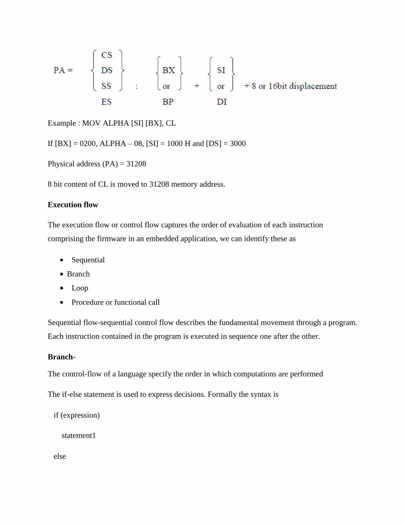
Example : MOV ALPHA [SI] [BX], CL
If [BX] = 0200, ALPHA – 08, [SI] = 1000 H and [DS] = 3000
Physical address (PA) = 31208
8 bit content of CL is moved to 31208 memory address.
Execution flow
The execution flow or control flow captures the order of evaluation of each instruction
comprising the firmware in an embedded application, we can identify these as
Sequential
Branch
Loop
Procedure or functional call
Sequential flow-sequential control flow describes the fundamental movement through a program.
Each instruction contained in the program is executed in sequence one after the other.
Branch-
The control-flow of a language specify the order in which computations are performed
The if-else statement is used to express decisions. Formally the syntax is
if (expression)
statement1
else
statement2
Where the else part is optional. The expression is evaluated; if it is true (that is, if expression has
a nonzero value), statement1 is executed. If it is false (expression is zero) and if there is an else
part, statement2 is executed instead.
Since a if tests the numeric value of an expression, certain coding shortcuts are possible. The
most obvious is writing
if (expression)
Instead of
if (expression != 0)
Sometimes this is natural and clear; at other times it can be cryptic
Procedure or function call
The procedure or function invocation is the most complex of the flow of control constructs.
CALL operand - when PC is unconditionally saved and replaced by specified operand; the
control is transferred to specified memory location.
RET – Previously saved contents of PC are restored, and control is returned to previous context.
Arithmetic and logic
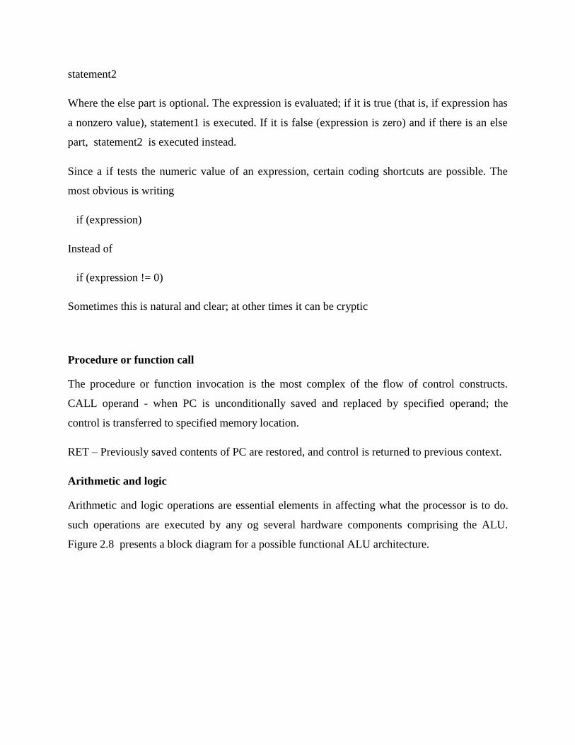
Arithmetic and logic operations are essential elements in affecting what the processor is to do.
such operations are executed by any og several hardware components comprising the ALU.
Figure 2.8 presents a block diagram for a possible functional ALU architecture.
t Datapath
Figure 2.8 A block diagram for a possible functional ALU architecture.
Data is brought into the ALU and held in the local registers. The opcode is decoded, the
appropriate operation is performed on the selected operands, and the result is stored in another
local register.
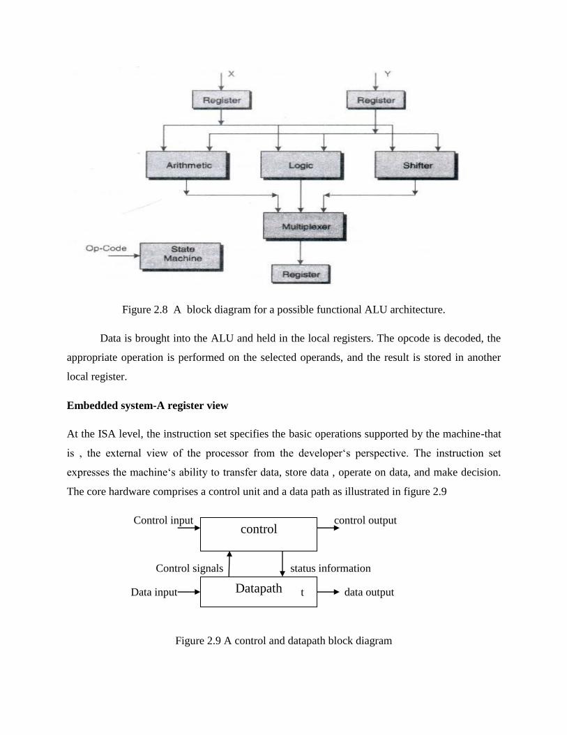
Embedded system-A register view
At the ISA level, the instruction set specifies the basic operations supported by the machine-that
is , the external view of the processor from the developer‘s perspective. The instruction set
expresses the machine‘s ability to transfer data, store data , operate on data, and make decision.
The core hardware comprises a control unit and a data path as illustrated in figure 2.9
Control input control
control output
Control signals status information
Data input data output
Figure 2.9 A control and datapath block diagram
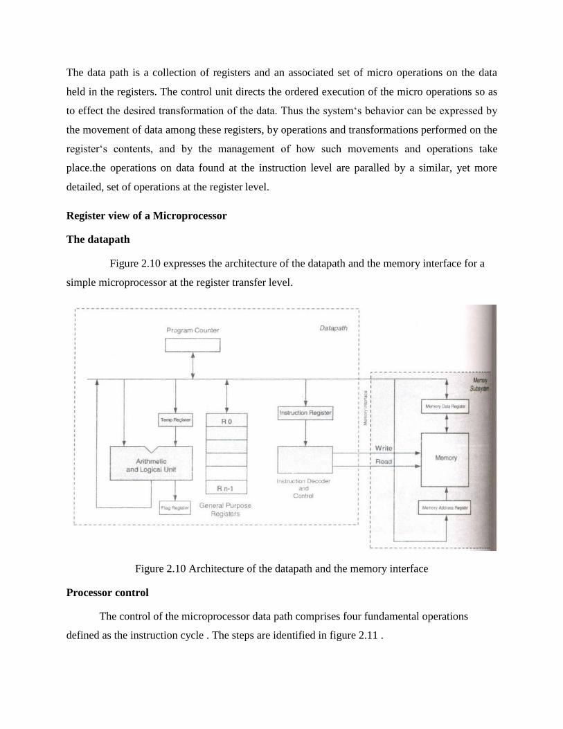
The data path is a collection of registers and an associated set of micro operations on the data
held in the registers. The control unit directs the ordered execution of the micro operations so as
to effect the desired transformation of the data. Thus the system‘s behavior can be expressed by
the movement of data among these registers, by operations and transformations performed on the
register‘s contents, and by the management of how such movements and operations take
place.the operations on data found at the instruction level are paralled by a similar, yet more
detailed, set of operations at the register level.
Register view of a Microprocessor
The datapath
Figure 2.10 expresses the architecture of the datapath and the memory interface for a
simple microprocessor at the register transfer level.
Figure 2.10 Architecture of the datapath and the memory interface
Processor control
The control of the microprocessor data path comprises four fundamental operations
defined as the instruction cycle . The steps are identified in figure 2.11 .
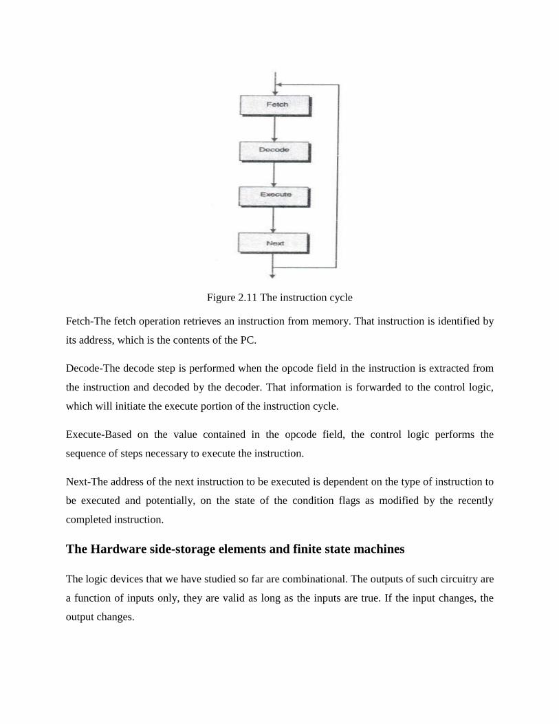
Figure 2.11 The instruction cycle
Fetch-The fetch operation retrieves an instruction from memory. That instruction is identified by
its address, which is the contents of the PC.
Decode-The decode step is performed when the opcode field in the instruction is extracted from
the instruction and decoded by the decoder. That information is forwarded to the control logic,
which will initiate the execute portion of the instruction cycle.
Execute-Based on the value contained in the opcode field, the control logic performs the
sequence of steps necessary to execute the instruction.
Next-The address of the next instruction to be executed is dependent on the type of instruction to
be executed and potentially, on the state of the condition flags as modified by the recently
completed instruction.
The Hardware side-storage elements and finite state machines
The logic devices that we have studied so far are combinational. The outputs of such circuitry are
a function of inputs only, they are valid as long as the inputs are true. If the input changes, the
output changes.
The concepts of State and Time
Time - A combinational logic system has no notion of time or history. The present output does
not depend in any way on how the output values are achieved. Neglecting the delays through the
system, we find that the output is immediate and a direct function of the current input set. Time
is an integral part of the behavior of a system.
State -In an analog circuits, we define branch and mesh currents and branch or node voltages.
The values these variables assume over time characterize the behavior of that circuit. If we know
the values of the specified variables over time, we know the behavior of the circuit. Such
variables are called state variables. We define the state of a system at any time as a set of values
for such variables; each set of values represents a unique state.
State changes
In traditional logic, a simple memory device, represented by a single variable, has two states
binary 1 and 0. The device will remain in the state until changed. For a set of variables, the state
changes with time are called the behavior of a system.
The state diagram
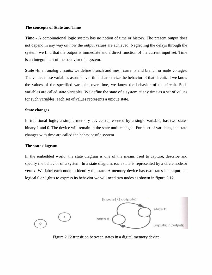
In the embedded world, the state diagram is one of the means used to capture, describe and
specify the behavior of a system. In a state diagram, each state is represented by a circle,node,or
vertex. We label each node to identify the state. A memory device has two states-its output is a
logical 0 or 1,thus to express its behavior we will need two nodes as shown in figure 2.12.
Figure 2.12 transition between states in a digital memory device
We show the transition between two states using a labeled directed line or arrow called arc as
illustrated in figure because the line has a direction, the state diagram is referred to as a directed
graph. The head o point of the arrow identifies the final state, and the tail or back of the arrow
identifies the initial state.
Finite-state machine (FSM)- A theoretical model
A finite-state machine (FSM) or finite-state automaton (plural: automata), or simply
a state machine, is a mathematical model of computation used to design both computer
programs and sequential logic circuits. It is conceived as an abstract machine that can be in one
of a finite number of states. The machine is in only one state at a time; the state it is in at any
given time is called the current state. It can change from one state to another when initiated by a
triggering event or condition; this is called a transition. A particular FSM is defined by a list of
its states, and the triggering condition for each transition.
The behavior of state machines can be observed in many devices in modern society
which perform a predetermined sequence of actions depending on a sequence of events with
which they are presented. Simple examples are vending machines which dispense products when
the proper combination of coins are deposited, elevators which drop riders off at upper floors
before going down, traffic lights which change sequence when cars are waiting, and combination
locks which require the input of combination numbers in the proper order.
Finite-state machines can model a large number of problems, among which are electronic
design automation, communication protocol design, language parsing and other engineering
applications. In biology and artificial intelligence research, state machines or hierarchies of state
machines have been used to describe neurological systems and in linguistics—to describe
the grammars of natural languages.
Figure shows a simple finite-state machine having no inputs other than a clock and have
only primitive outputs. such machines are referred to as autonomous clocks. A high level block
diagram for a finite-state machine begins with the diagram in figure 2.13.
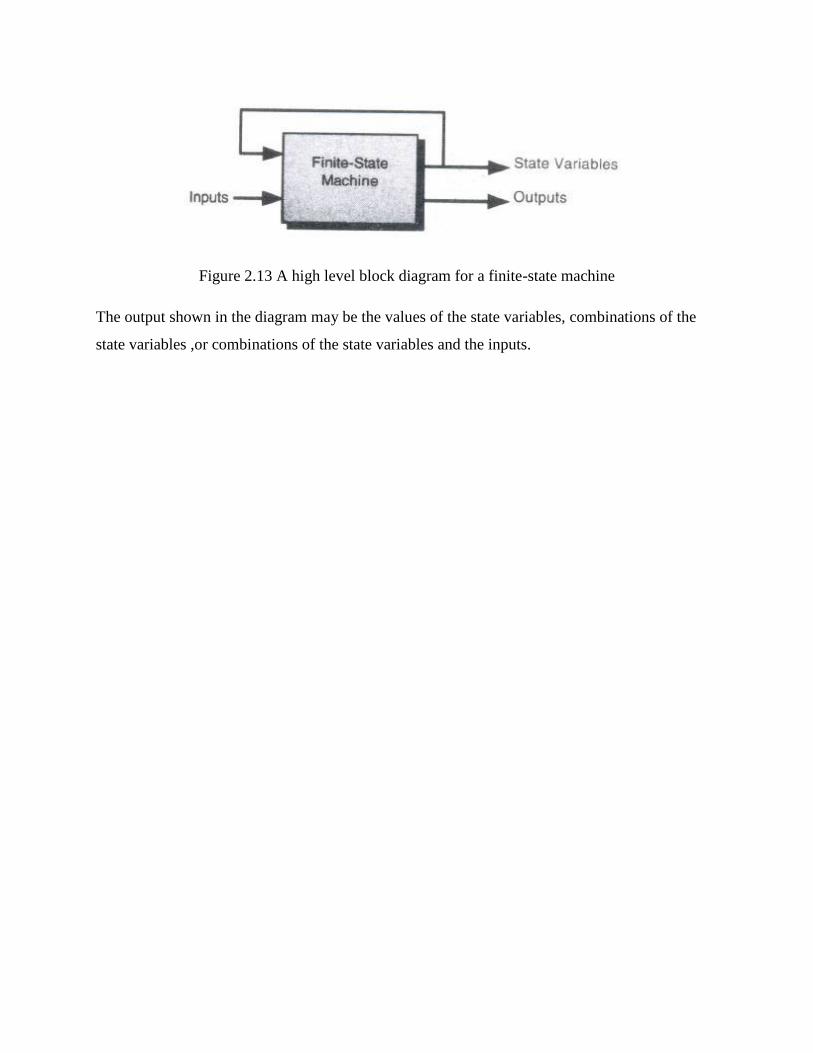
Figure 2.13 A high level block diagram for a finite-state machine
The output shown in the diagram may be the values of the state variables, combinations of the
state variables ,or combinations of the state variables and the inputs.
UNIT 3
Memory
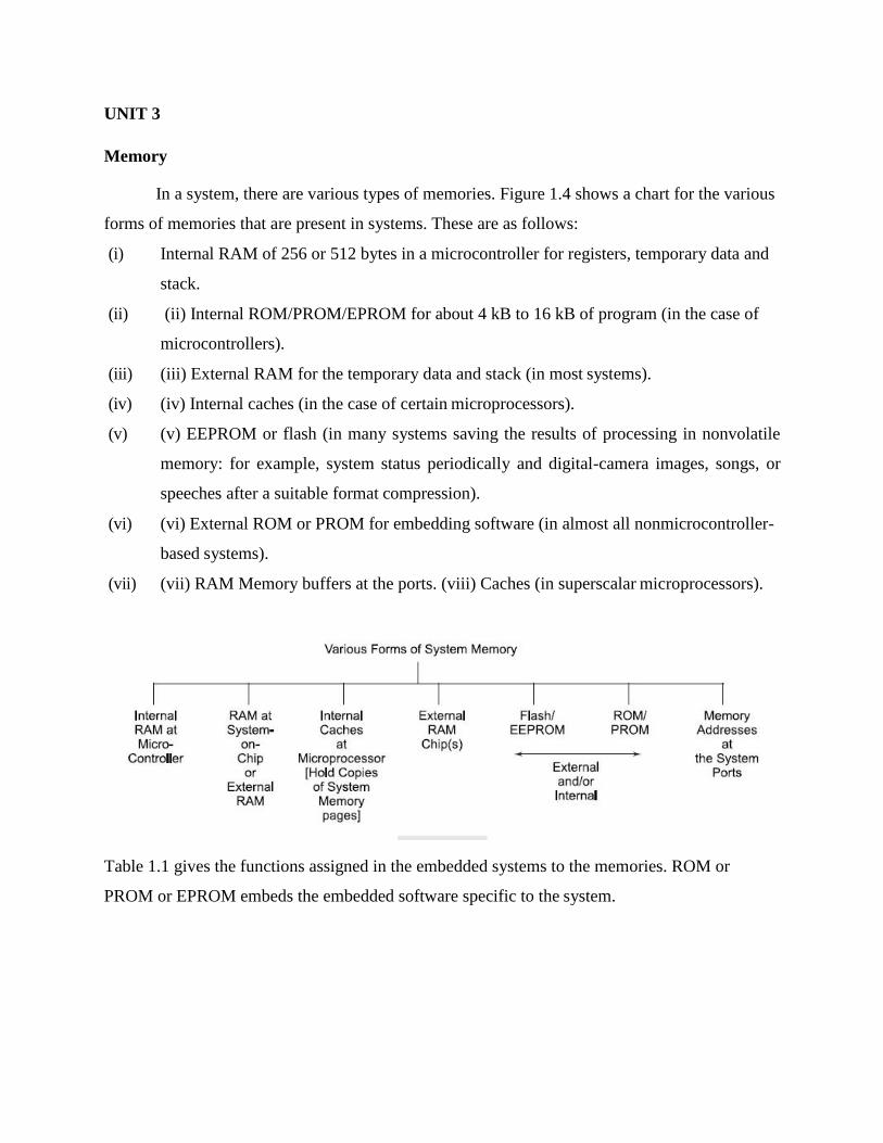
In a system, there are various types of memories. Figure 1.4 shows a chart for the various
forms of memories that are present in systems. These are as follows:
(i) Internal RAM of 256 or 512 bytes in a microcontroller for registers, temporary data and
stack.
(ii) (ii) Internal ROM/PROM/EPROM for about 4 kB to 16 kB of program (in the case of
microcontrollers).
(iii) (iii) External RAM for the temporary data and stack (in most systems).
(iv) (iv) Internal caches (in the case of certain microprocessors).
(v) (v) EEPROM or flash (in many systems saving the results of processing in nonvolatile
memory: for example, system status periodically and digital-camera images, songs, or
speeches after a suitable format compression).
(vi) (vi) External ROM or PROM for embedding software (in almost all nonmicrocontroller-
based systems).
(vii) (vii) RAM Memory buffers at the ports. (viii) Caches (in superscalar microprocessors).
Table 1.1 gives the functions assigned in the embedded systems to the memories. ROM or
PROM or EPROM embeds the embedded software specific to the system.
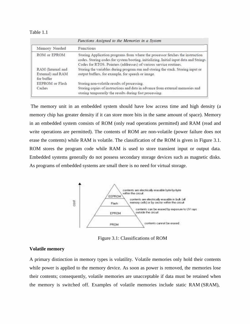
Table 1.1
The memory unit in an embedded system should have low access time and high density (a
memory chip has greater density if it can store more bits in the same amount of space). Memory
in an embedded system consists of ROM (only read operations permitted) and RAM (read and
write operations are permitted). The contents of ROM are non-volatile (power failure does not
erase the contents) while RAM is volatile. The classification of the ROM is given in Figure 3.1.
ROM stores the program code while RAM is used to store transient input or output data.
Embedded systems generally do not possess secondary storage devices such as magnetic disks.
As programs of embedded systems are small there is no need for virtual storage.
Figure 3.1: Classifications of ROM
Volatile memory
A primary distinction in memory types is volatility. Volatile memories only hold their contents
while power is applied to the memory device. As soon as power is removed, the memories lose
their contents; consequently, volatile memories are unacceptable if data must be retained when
the memory is switched off. Examples of volatile memories include static RAM (SRAM),
synchronous static RAM (SSRAM), synchronous dynamic RAM (SDRAM), and FPGA on-chip
memory.
Nonvolatile memory
Non-volatile memories retain their contents when power is switched off, making them good
choices for storing information that must be retrieved after a system power-cycle. Processor
boot-code, persistent application settings, and FPGA configurationdataaretypicallystoredinnon-
volatilememory.Althoughnon-volatile memory has the advantage of retaining its data when
power is removed, it is typically much slower to write to than volatile memory, and often has
more complex writing and erasing procedures. Non-volatile memory is also usually only
guaranteed to be erasable a given number of times, after which it may fail. Examples of non-
volatile memories include all types of flash, EPROM, and EEPROM. Most modern embedded
systems use some type of flash memory for non-volatile storage. Many embedded applications
require both volatile and non-volatile memories because the two memory types serve unique and
exclusive purposes. The following sections discuss the use of specific types of memory in
embedded systems.
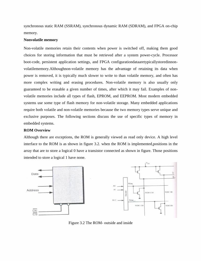
ROM Overview
Although there are exceptions, the ROM is generally viewed as read only device. A high level
interface to the ROM is as shown in figure 3.2. when the ROM is implemented,positions in the
array that are to store a logical 0 have a transistor connected as shown in figure. Those positions
intended to store a logical 1 have none.
Figure 3.2 The ROM- outside and inside
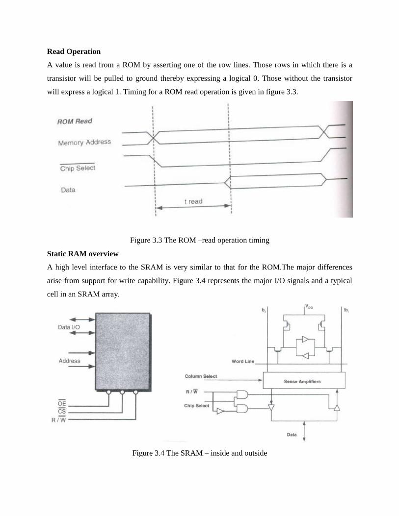
Read Operation
A value is read from a ROM by asserting one of the row lines. Those rows in which there is a
transistor will be pulled to ground thereby expressing a logical 0. Those without the transistor
will express a logical 1. Timing for a ROM read operation is given in figure 3.3.
Figure 3.3 The ROM –read operation timing
Static RAM overview
A high level interface to the SRAM is very similar to that for the ROM.The major differences
arise from support for write capability. Figure 3.4 represents the major I/O signals and a typical
cell in an SRAM array.
Figure 3.4 The SRAM – inside and outside
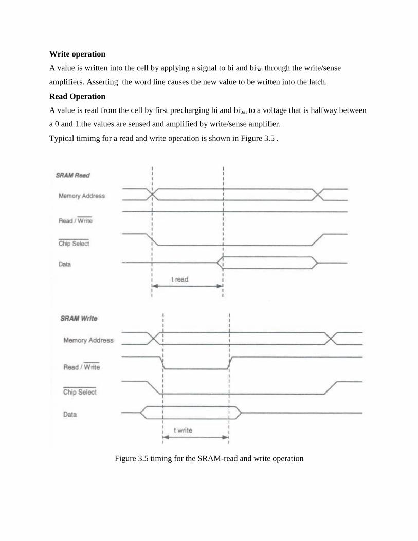
Write operation
A value is written into the cell by applying a signal to bi and bibar through the write/sense
amplifiers. Asserting the word line causes the new value to be written into the latch.
Read Operation
A value is read from the cell by first precharging bi and bibar to a voltage that is halfway between
a 0 and 1.the values are sensed and amplified by write/sense amplifier.
Typical timimg for a read and write operation is shown in Figure 3.5 .
Figure 3.5 timing for the SRAM-read and write operation
SDRAM
SDRAM is another type of volatile memory. It is similar to SRAM, except that it is
dynamic and must be refreshed periodically to maintain its content. The dynamic memory cells
in SDRAM are much smaller than the static memory cells used in SRAM. This difference in size
translates into very high-capacity and low-cost memory devices. In addition to the refresh
requirement, SDRAM has other very specific interface requirements which typically necessitate
the use of special controller hardware. Unlike SRAM, which has a static set of address lines,
SDRAM divides up its memory space into banks, rows, and columns. Switching between banks
and rows incurs some overhead, so that efficient use of SDRAM involves the careful ordering of
accesses. SDRAM also multiplexes the row and column addresses over the same address lines,
which reduces the pin count necessary to implement a given size of SDRAM. Higher speed
varieties of SDRAM such as DDR, DDR2, and DDR3 also have strict signal integrity
requirements which need to be carefully considered during the design of the PCB. SDRAM
devices are among the least expensive and largest-capacity types of RAM devices available,
making them one of the most popular. Most modern embedded systems use SDRAM. A major
part of an SDRAM interface is the SDRAM controller. The SDRAM controller manages all the
address-multiplexing, refresh and row and bank switching tasks, allowing the rest of the system
to access SDRAM without knowledge of its internal architecture.
Dynamic RAM Overview
Larger microcomputer systems use Dynamic RAM (DRAM) rather than Static RAM (SRAM)
because of its lower cost per bit. DRAMs require more complex interface circuitry because of
their multiplexed address bus and because of the need to refresh each memory cell periodically.
A typical DRAM memory is laid out as a square array of memory cells with an equal number of
rows and columns. Each memory cell stores one bit. The bits are addressed by using half of the
bits (the most significant half) to select a row and the other half to select a column.
Each DRAM memory cell is very simple – it consists of a capacitor and a MOSFET switch. A
DRAM memory cell is therefore much smaller than an SRAM cell which needs at least two gates
to implement a flip-flop. A typical DRAM array appears as illustrated in figure 3.6 .
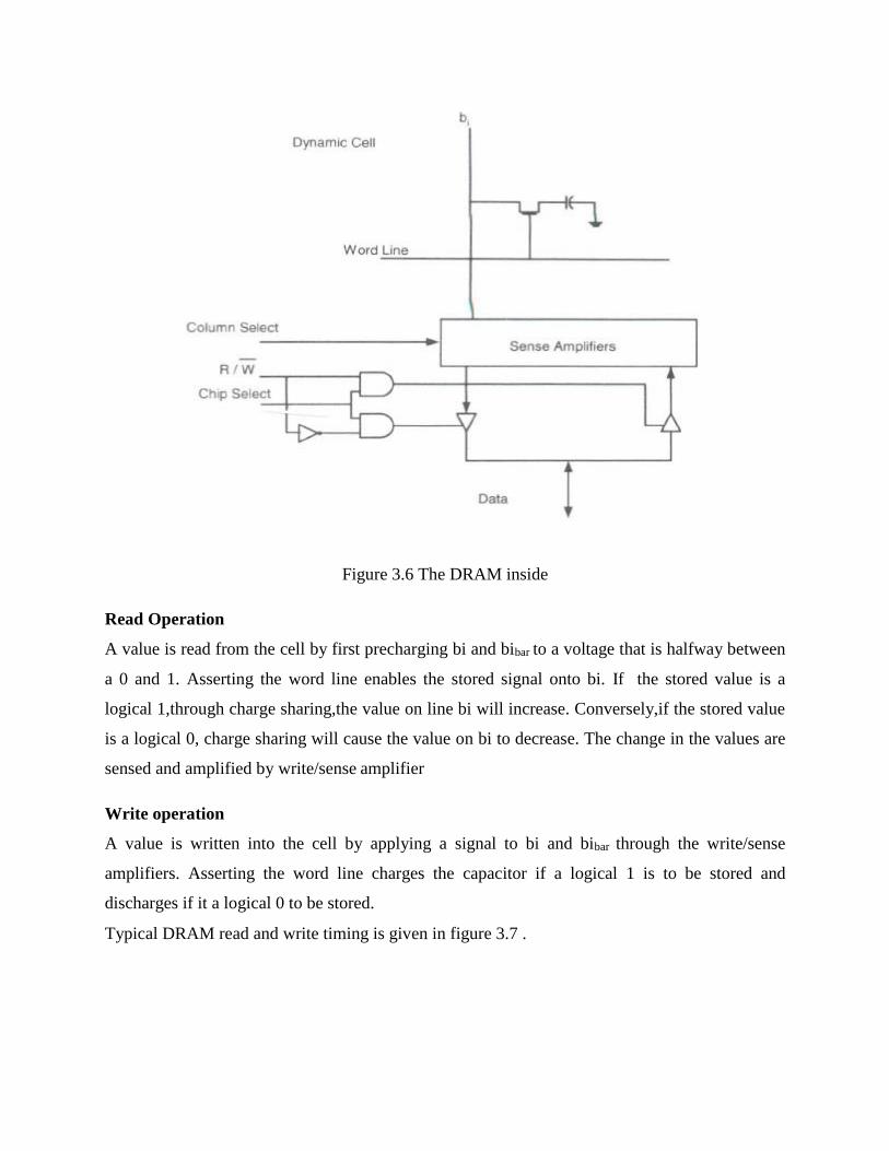
Figure 3.6 The DRAM inside
Read Operation
A value is read from the cell by first precharging bi and bibar to a voltage that is halfway between
a 0 and 1. Asserting the word line enables the stored signal onto bi. If the stored value is a
logical 1,through charge sharing,the value on line bi will increase. Conversely,if the stored value
is a logical 0, charge sharing will cause the value on bi to decrease. The change in the values are
sensed and amplified by write/sense amplifier
Write operation
A value is written into the cell by applying a signal to bi and bibar through the write/sense
amplifiers. Asserting the word line charges the capacitor if a logical 1 is to be stored and
discharges if it a logical 0 to be stored.
Typical DRAM read and write timing is given in figure 3.7 .
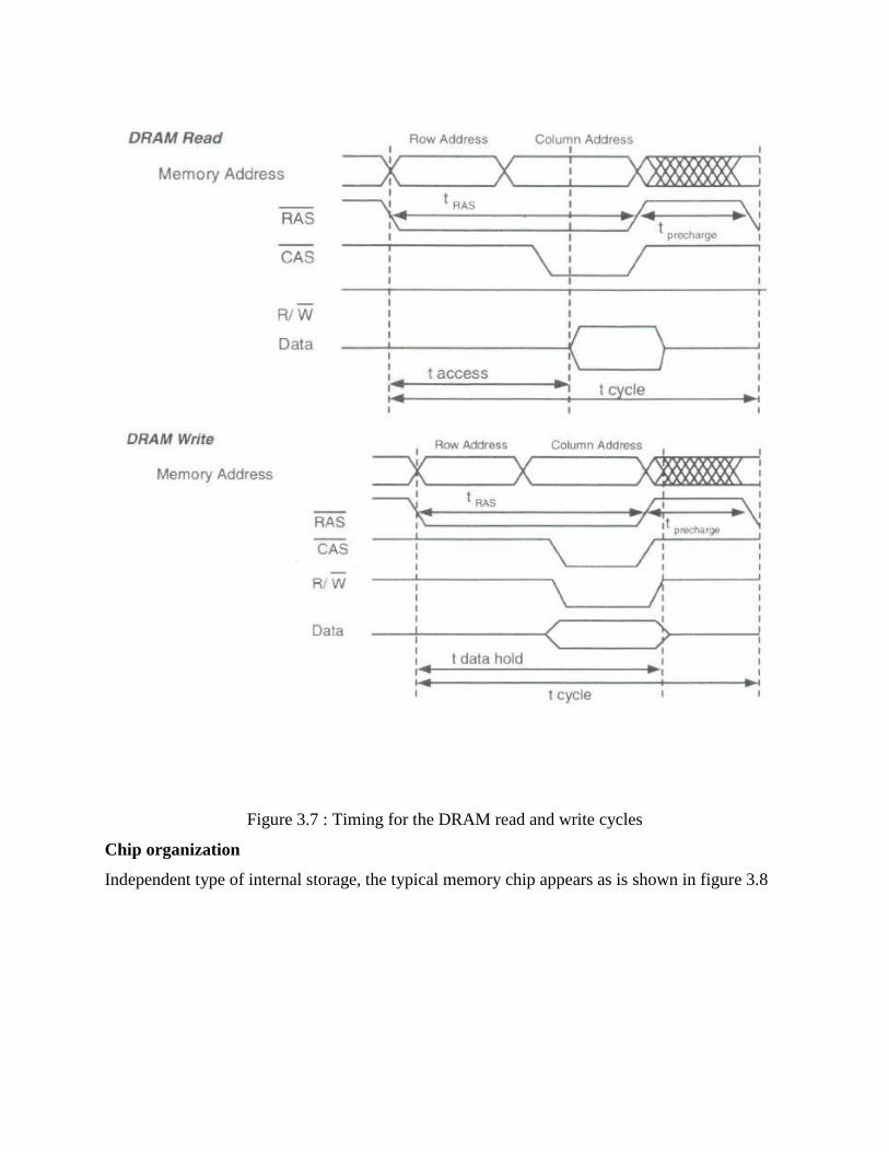
Figure 3.7 : Timing for the DRAM read and write cycles
Chip organization
Independent type of internal storage, the typical memory chip appears as is shown in figure 3.8
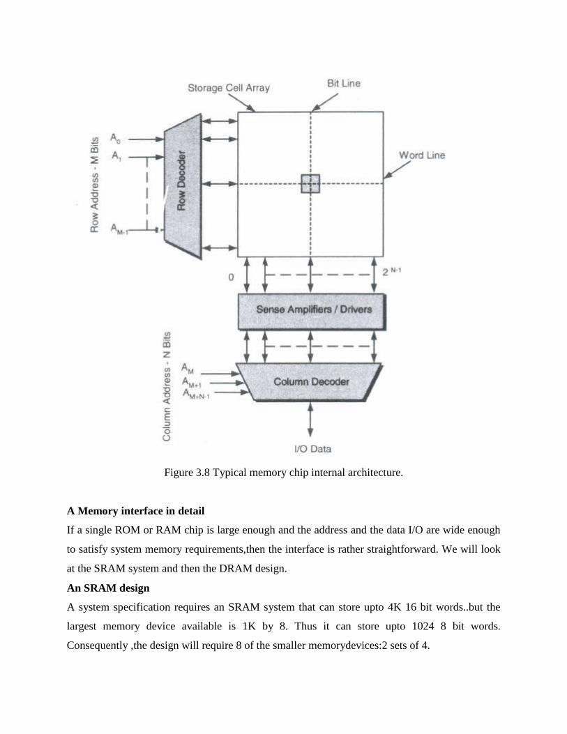
Figure 3.8 Typical memory chip internal architecture.
A Memory interface in detail
If a single ROM or RAM chip is large enough and the address and the data I/O are wide enough
to satisfy system memory requirements,then the interface is rather straightforward. We will look
at the SRAM system and then the DRAM design.
An SRAM design
A system specification requires an SRAM system that can store upto 4K 16 bit words..but the
largest memory device available is 1K by 8. Thus it can store upto 1024 8 bit words.
Consequently ,the design will require 8 of the smaller memorydevices:2 sets of 4.
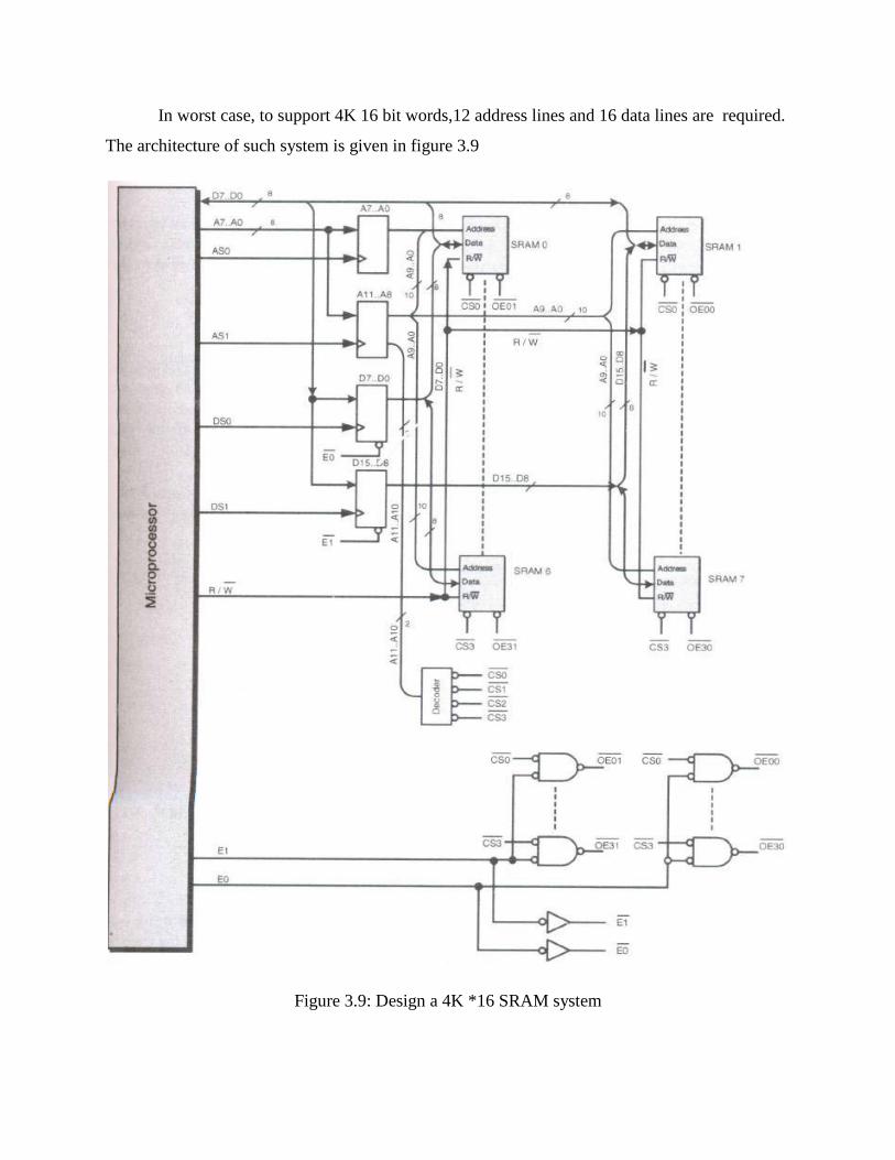
In worst case, to support 4K 16 bit words,12 address lines and 16 data lines are required.
The architecture of such system is given in figure 3.9
Figure 3.9: Design a 4K *16 SRAM system
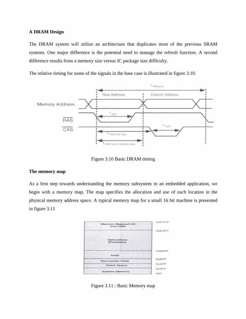
A DRAM Design
The DRAM system will utilize an architecture that duplicates most of the previous SRAM
systems. One major difference is the potential need to manage the refresh function. A second
difference results from a memory size versus IC package size difficulty.
The relative timing for some of the signals in the base case is illustrated in figure 3.10.
Figure 3.10 Basic DRAM timing
The memory map
As a first step towards understanding the memory subsystem in an embedded application, we
begin with a memory map. The map specifies the allocation and use of each location in the
physical memory address space. A typical memory map for a small 16 bit machine is presented
in figure 3.11
Figure 3.11 : Basic Memory map
This is the primary physical memory. From a high level perspective, the memory subsystem is
comprised of two basic types:ROM and RAM. It is possible for the required code and data space
to exceed total available primary memory.under such circumstances, one must use techniques
called virtual memory and overlays to accommodate the expanded needs.
Memory subsystem Architecture
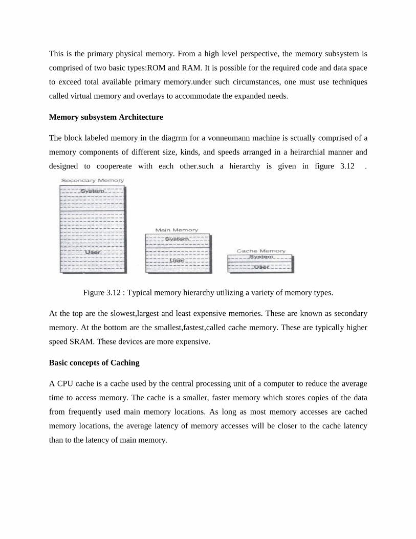
The block labeled memory in the diagrrm for a vonneumann machine is sctually comprised of a
memory components of different size, kinds, and speeds arranged in a heirarchial manner and
designed to coopereate with each other.such a hierarchy is given in figure 3.12 .
Figure 3.12 : Typical memory hierarchy utilizing a variety of memory types.
At the top are the slowest,largest and least expensive memories. These are known as secondary
memory. At the bottom are the smallest,fastest,called cache memory. These are typically higher
speed SRAM. These devices are more expensive.
Basic concepts of Caching
A CPU cache is a cache used by the central processing unit of a computer to reduce the average
time to access memory. The cache is a smaller, faster memory which stores copies of the data
from frequently used main memory locations. As long as most memory accesses are cached
memory locations, the average latency of memory accesses will be closer to the cache latency
than to the latency of main memory.
Data is transferred between memory and cache in blocks of fixed size, called cache lines. When a
cache line is copied from memory into the cache, a cache entry is created. The cache entry will
include the copied data as well as the requested memory location (now called a tag).
When the processor needs to read or write a location in main memory, it first checks for a
corresponding entry in the cache. The cache checks for the contents of the requested memory
location in any cache lines that might contain that address. If the processor finds that the memory
location is in the cache, a cache hit has occurred. However, if the processor does not find the
memory location in the cache, a cache miss has occurred. In the case of:
a cache hit, the processor immediately reads or writes the data in the cache line.
a cache miss, the cache allocates a new entry, and copies in data from main memory. Then,
the request is fulfilled from the contents of the cache.
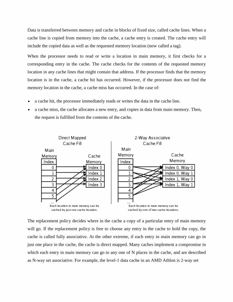
The replacement policy decides where in the cache a copy of a particular entry of main memory
will go. If the replacement policy is free to choose any entry in the cache to hold the copy, the
cache is called fully associative. At the other extreme, if each entry in main memory can go in
just one place in the cache, the cache is direct mapped. Many caches implement a compromise in
which each entry in main memory can go to any one of N places in the cache, and are described
as N-way set associative. For example, the level-1 data cache in an AMD Athlon is 2-way set
associative, which means that any particular location in main memory can be cached in either of
2 locations in the level-1 data cache.
Associativity is a trade-off. If there are ten places to which the replacement policy could
have mapped a memory location, then to check if that location is in the cache, ten cache entries
must be searched. Checking more places takes more power, chip area, and potentially time. On
the other hand, caches with more associativity suffer fewer misses so that the CPU wastes less
time reading from the slow main memory. The rule of thumb is that doubling the associativity,
from direct mapped to 2-way, or from 2-way to 4-way, has about the same effect on hit rate as
doubling the cache size. Associativity increases beyond 4-way have much less effect on the hit
rate and are generally done for other reasons
In order of worse but simple to better but complex:
direct mapped cache — The best (fastest) hit times, and so the best tradeoff for "large"
caches
2-way set associative cache
2-way skewed associative cache – In 1993, this was the best tradeoff for caches whose sizes
were in the range 4K-8K bytes.
4-way set associative cache
fully associative cache – the best (lowest) miss rates, and so the best tradeoff when the miss
penalty is very high
Direct-mapped cache
Here each location in main memory can only go in one entry in the cache. It doesn't have a
replacement policy as such, since there is no choice of which cache entry's contents to evict. This
means that if two locations map to the same entry, they may continually knock each other out.
Although simpler, a direct-mapped cache needs to be much larger than an associative one to give
comparable performance, and is more unpredictable. Let 'x' be block number in cache, 'y' be
block number of memory, and 'n' be number of blocks in cache, then mapping is done with the
help of the equation x=y mod n.
2- way set associative cache
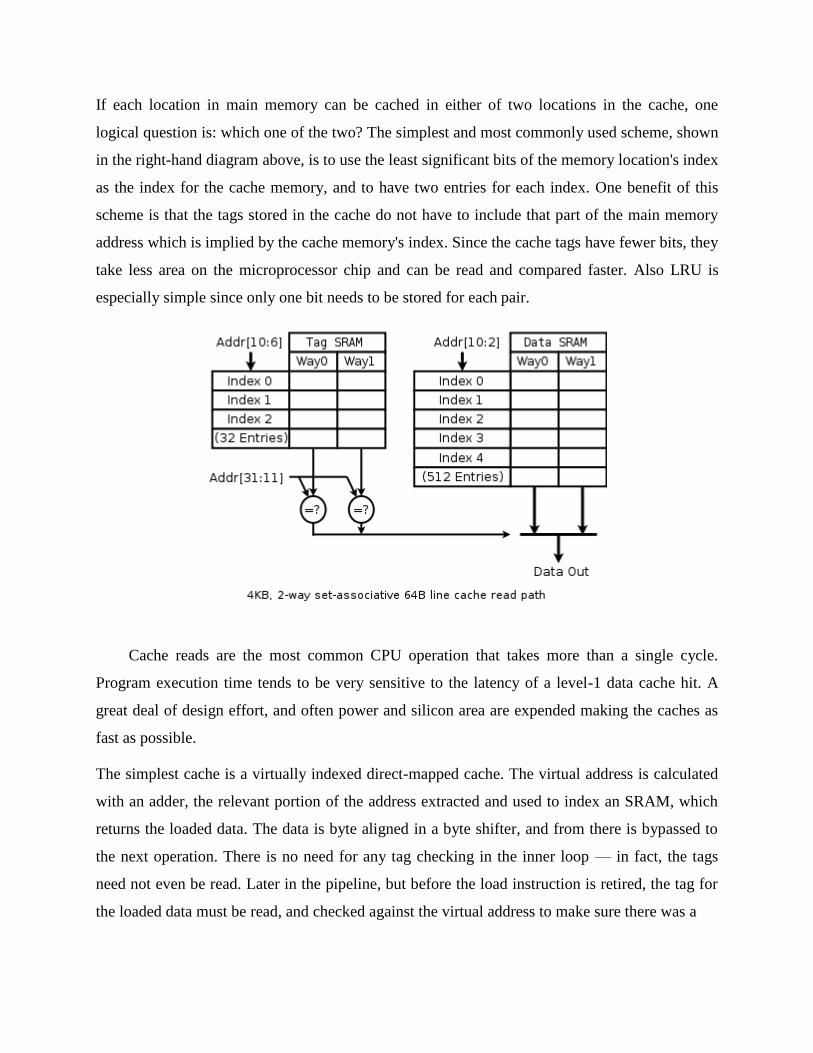
If each location in main memory can be cached in either of two locations in the cache, one
logical question is: which one of the two? The simplest and most commonly used scheme, shown
in the right-hand diagram above, is to use the least significant bits of the memory location's index
as the index for the cache memory, and to have two entries for each index. One benefit of this
scheme is that the tags stored in the cache do not have to include that part of the main memory
address which is implied by the cache memory's index. Since the cache tags have fewer bits, they
take less area on the microprocessor chip and can be read and compared faster. Also LRU is
especially simple since only one bit needs to be stored for each pair.
Cache reads are the most common CPU operation that takes more than a single cycle.
Program execution time tends to be very sensitive to the latency of a level-1 data cache hit. A
great deal of design effort, and often power and silicon area are expended making the caches as
fast as possible.
The simplest cache is a virtually indexed direct-mapped cache. The virtual address is calculated
with an adder, the relevant portion of the address extracted and used to index an SRAM, which
returns the loaded data. The data is byte aligned in a byte shifter, and from there is bypassed to
the next operation. There is no need for any tag checking in the inner loop — in fact, the tags
need not even be read. Later in the pipeline, but before the load instruction is retired, the tag for
the loaded data must be read, and checked against the virtual address to make sure there was a
cache hit. On a miss, the cache is updated with the requested cache line and the pipeline is
restarted.
An associative cache is more complicated, because some form of tag must be read to determine
which entry of the cache to select. An N-way set-associative level-1 cache usually reads all N
possible tags and N data in parallel, and then chooses the data associated with the matching tag.
Level-2 caches sometimes save power by reading the tags first, so that only one data element is
read from the data SRAM.
The diagram to the right is intended to clarify the manner in which the various fields of the
address are used. Address bit 31 is most significant, bit 0 is least significant. The diagram shows
the SRAMs, indexing, and multiplexing for a 4 kB, 2-way set-associative, virtually indexed and
virtually tagged cache with 64 B lines, a 32b read width and 32b virtual address.
Because the cache is 4 kB and has 64 B lines, there are just 64 lines in the cache, and we read
two at a time from a Tag SRAM which has 32 rows, each with a pair of 21 bit tags. Although
any function of virtual address bits 31 through 6 could be used to index the tag and data SRAMs,
it is simplest to use the least significant bits.
Similarly, because the cache is 4 kB and has a 4 B read path, and reads two ways for each access,
the Data SRAM is 512 rows by 8 bytes wide.
A more modern cache might be 16 kB, 4-way set-associative, virtually indexed, virtually hinted,
and physically tagged, with 32 B lines, 32b read width and 36b physical addresses. The read path
recurrence for such a cache looks very similar to the path above. Instead of tags, vhints are read,
and matched against a subset of the virtual address. Later on in the pipeline, the virtual address is
translated into a physical address by the TLB, and the physical tag is read (just one, as the vhint
supplies which way of the cache to read). Finally the physical address is compared to the
physical tag to determine if a hit has occurred.
Dynamic memory allocation
Memory management is the act of managing computer memory. The essential requirement of
memory management is to provide ways to dynamically allocate portions of memory to
programs at their request, and freeing it for reuse when no longer needed. This is critical to the
computer system.
Several methods have been devised that increase the effectiveness of memory
management. Virtual memory systems separate the memory addresses used by a process from
actual physical addresses, allowing separation of processes and increasing the effectively
available amount of RAM using paging or swapping to secondary storage. The quality of the
virtual memory manager can have an extensive effect on overall system performance.
The task of fulfilling an allocation request consists of locating a block of unused memory of
sufficient size. Memory requests are satisfied by allocating portions from a large pool of memory
called the heap. At any given time, some parts of the heap are in use, while some are "free"
(unused) and thus available for future allocations. Several issues complicate implementation,
such as internal and external fragmentation, which arises when there are many small gaps
between allocated memory blocks, which invalidates their use for an allocation request. The
allocator'smetadata can also inflate the size of (individually) small allocations. This is managed
often by chunking. The memory management system must track outstanding allocations to
ensure that they do not overlap and that no memory is ever "lost" as a memory leak.
We are more concerned with managing main memory to accommodate
programs larger than main memory
multiple processes in main memory.
Multiple programs in main memory.
Overlays
An overlay is a poor man‘s version of virtual memory. The overlay will be in ROM and used to
accommodate a program that is larger than main memory. The program is segmented into a
number of sections called overlays. The sections are
Top level routine.
Code to perform overlay process.
Data segment for shared data.
Overlay segment.
UNIT 5
EMBEDDED SYSTEM DESIGN AND DEVELOPMENT
LIFE CYCLE MODELS
The fundamentals of design are
Find out what the customers want.
Think of a way to give them what they want.
Prove what you have done by building and testing it.
Build a lot of the product to prove that it wasn‘t an accident.
Use the product to solve the customer‘s problem.
The common life cycle models are:
Waterfall model
V cycle model.
Spiral
Rapid prototype
Waterfall model
The waterfall model represents a cycle- specifically a series of steps appearing much like a
waterfall. It is the model which is use to linear process development. It is a sequential design
process, often used in software process development in which progress is seen as flowing
steadily downwards through the phases of Conception, Initiation, Analysis, Design,
Construction, Testing, Production/Implementation and Maintenance. Figure 4.1 shows the
water life cycle model
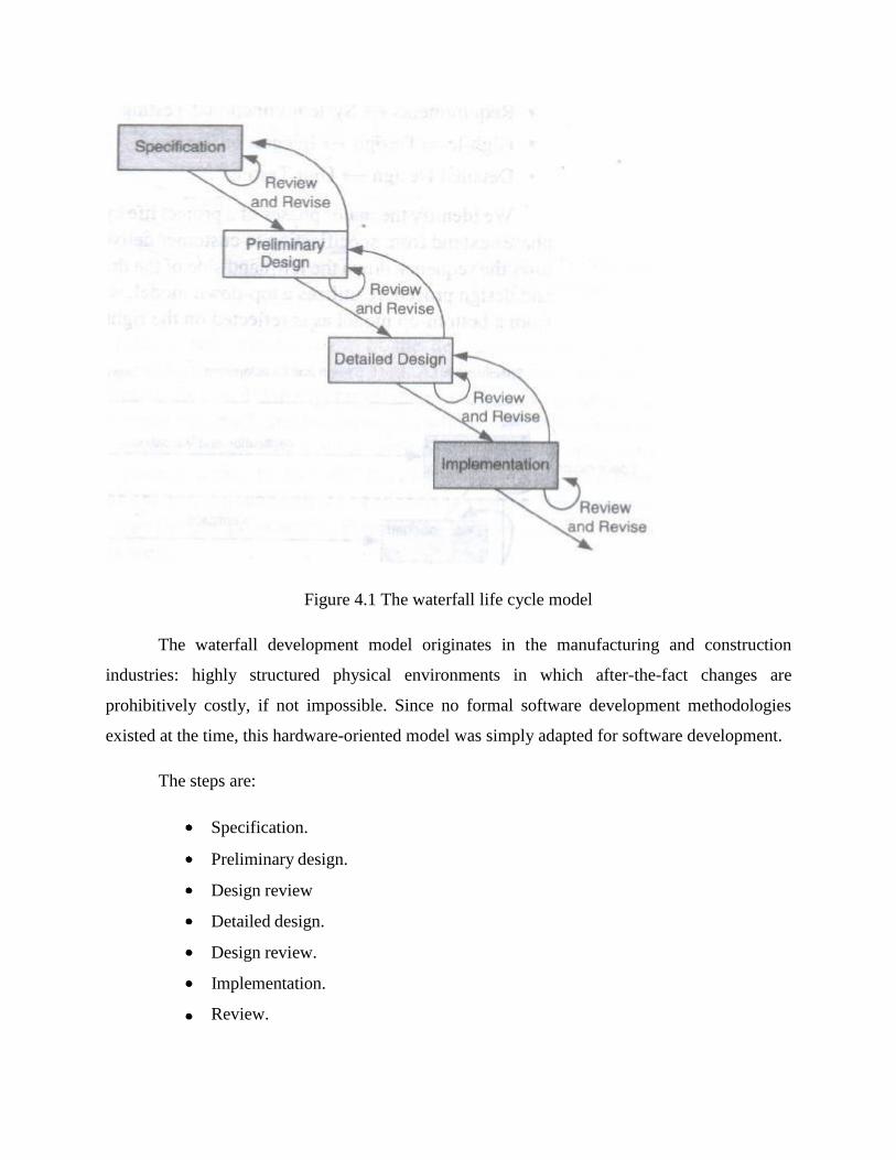
Figure 4.1 The waterfall life cycle model
The waterfall development model originates in the manufacturing and construction
industries: highly structured physical environments in which after-the-fact changes are
prohibitively costly, if not impossible. Since no formal software development methodologies
existed at the time, this hardware-oriented model was simply adapted for software development.
The steps are:
Specification.
Preliminary design.
Design review
Detailed design.
Design review.
Implementation.
Review.
Phases:
1) Requirement : In this phase we gather necessary information which will use for
development of any project . For above example we gather information like which types of
characteristics client wants. It also defines system requirement specification. This phase defines
what to do.
2) Design: In design phase we then construct design to how to implement that requirements
gathered into phase 1 .This phase define how to do .For this phase we then write algorithms
3) Coding: Now base on design phase we then write actual code to implement algorithms. This
code should be efficient.
4) Testing : This phase use to test our coding part it checks all the validation...like our code
should work for each and every possibilities of input if any bug occur then we have to report
that bug to design phase or development phase.
5) Maintenance: In this phase we need keep updating information.
1. The implementation process contains software preparation and transition activities, such as the
conception and creation of the maintenance plan; the preparation for handling problems
identified during development; and the followup on product configuration management.
2. The problem and modification analysis process, which is executed once the application has
become the responsibility of the maintenance group. The maintenance programmer must analyze
each request, confirm it (by reproducing the situation) and check its validity, investigate it and
propose a solution, document the request and the solution proposal, and, finally, obtain all the
required authorizations to apply the modifications.
3. The process considering the implementation of the modification itself.
4. The process acceptance of the modification, by confirming the modified work with the
individual who submitted the request in order to make sure the modification provided a solution.
5. The migration process is exceptional, and is not part of daily maintenance tasks. If the
software must be ported to another platform without any change in functionality, this process
will be used and a maintenance project team is likely to be assigned to this task.
6. Finally, the last maintenance process, also an event which does not occur on a daily basis, is
the retirement of a piece of software.
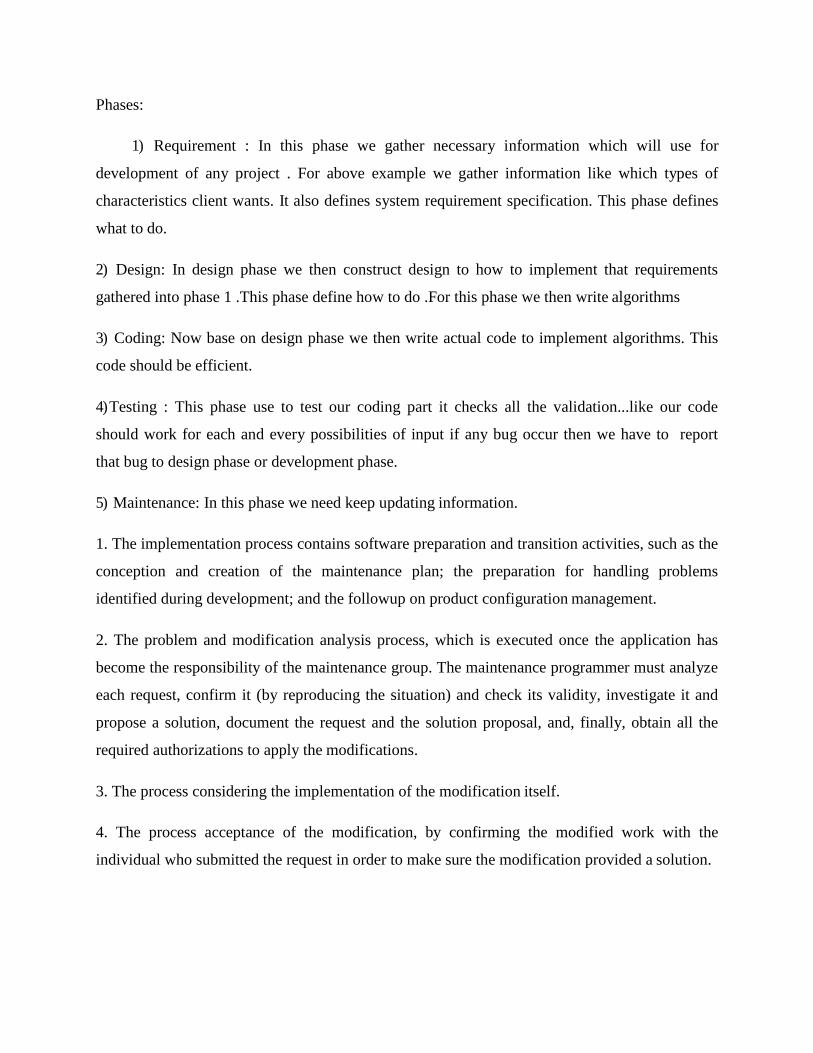
The V model
The V-Model is a term applied to a range of models, from a conceptual model designed to
produce a simplified understanding of the complexity associated with systems development to
detailed, rigorous development lifecycle models and project management models. Each test
phase is identified with its matching development phase as shown in figure 4.2.
Figure 4.2 : The V life cycle model
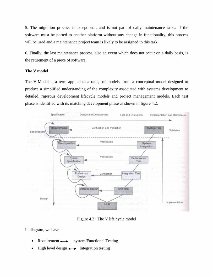
In diagram, we have
Requirement system/Functional Testing
High level design Integration testing
Detailed design Unit testing
The V-model is a graphical representation of the systems development lifecycle. It summarizes
the main steps to be taken in conjunction with the corresponding deliverables
within computerized system validation framework.
The V represents the sequence of steps in a project life cycle development. It describes the
activities to be performed and the results that have to be produced during product development.
The left side of the "V" represents the decomposition of requirements, and creation of system
specifications. The right side of the V represents integration of parts and their validation
Validation. The assurance that a product, service, or system meets the needs of the customer
and other identified stakeholders. It often involves acceptance and suitability with external
customers. Contrast with verification."
"Verification. The evaluation of whether or not a product, service, or system complies with a
regulation, requirement, specification, or imposed condition. It is often an internal process.
Contrast with validation."
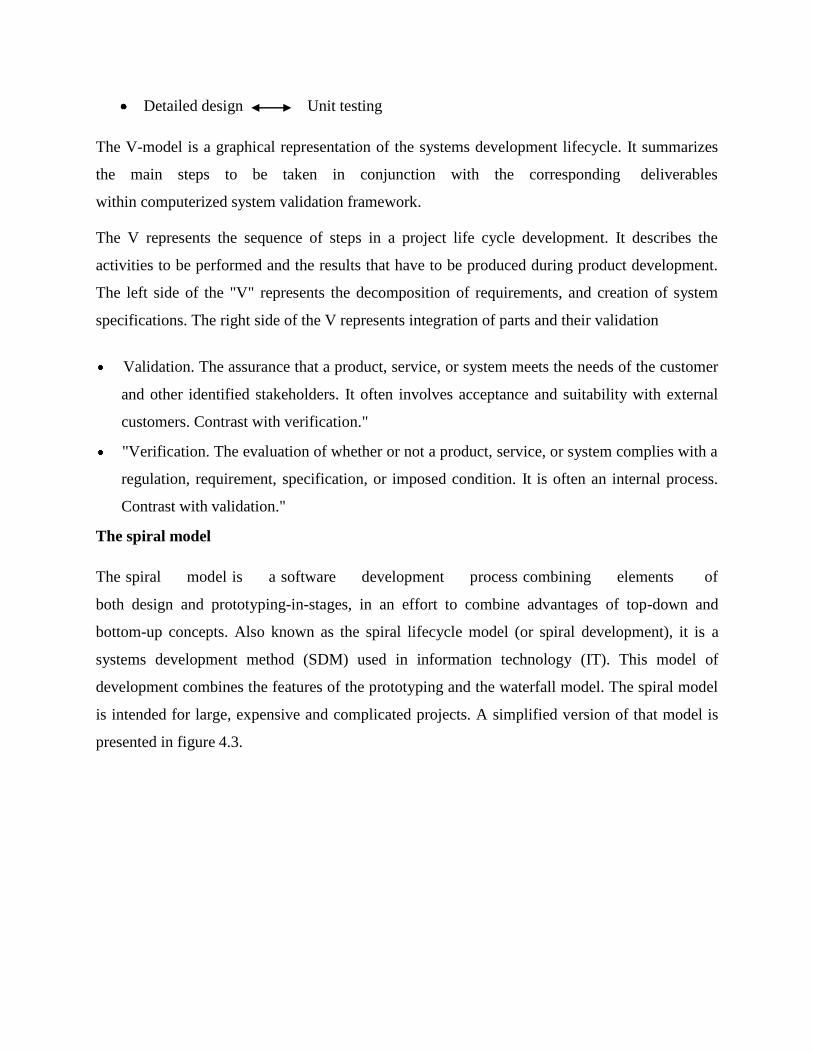
The spiral model
The spiral model is a software development process combining elements of
both design and prototyping-in-stages, in an effort to combine advantages of top-down and
bottom-up concepts. Also known as the spiral lifecycle model (or spiral development), it is a
systems development method (SDM) used in information technology (IT). This model of
development combines the features of the prototyping and the waterfall model. The spiral model
is intended for large, expensive and complicated projects. A simplified version of that model is
presented in figure 4.3.
Figure 4.3 The spiral life cycle model steps
The steps in spiral model life cycle are
Determine objective,alternatives,and constraints.
Identify and resolve risks.
Evaluate alternatives.
Develop deliverables-verify that they are correct.
Plan the next iteration.
Commit to an approach for the next iteration.
The spiral model combines the idea of iterative development (prototyping) with the systematic,
controlled aspects of the waterfall model. It allows for incremental releases of the product, or
incremental refinement through each time around the spiral. The spiral model also explicitly
includes risk management within software development. Identifying major risks, both technical
and managerial, and determining how to lessen the risk helps keep the software development
process under control.
The spiral model is based on continuous refinement of key products for requirements definition
and analysis, system and software design, and implementation (the code). At each iteration
around the cycle, the products are extensions of an earlier product. This model uses many of the
same phases as the waterfall model, in essentially the same order, separated by planning, risk
assessment, and the building of prototypes and simulations
Documents are produced when they are required, and the content reflects the information
necessary at that point in the process. All documents will not be created at the beginning of the
process, nor all at the end (hopefully). Like the product they define, the documents are works in
progress. The idea is to have a continuous stream of products produced and available for user
review.
The spiral lifecycle model allows for elements of the product to be added in when they become
available or known. This assures that there is no conflict with previous requirements and design.
This method is consistent with approaches that have multiple software builds and releases and
allows for making an orderly transition to a maintenance activity. Another positive aspect is that
the spiral model forces early user involvement in the system development effort. For projects
with heavy user interfacing, such as user application programs or instrument interface
applications, such involvement is helpful
Note that the requirements activity takes place in multiple sections and in multiple iterations, just
as planning and risk analysis occur in multiple places. Final design, implementation, integration,
and test occur in iteration 4. The spiral can be repeated multiple times for multiple builds. Using
this method of development, some functionality can be delivered to the user faster than the
waterfall method. The spiral method also helps manage risk and uncertainty by allowing multiple
decision points and by explicitly admitting that all of anything cannot be known before the
subsequent activity starts.
Rapid prototype
The Rapid prototyping model is intended to provide a rapid implementation of high level
portions of both the software and the hardware . the approach allows developers to construct
working portion of hardware and software in incremental stages.Each stage through the
cycle,one incorporates a little more of the intended functionality.The prototype is useful for both
the designer and the customer. The prototype can be either evolutionary or throughway. It has
the advantage of having a working system early in development process.
Problem solving-five steps to design
The 5 steps to a successful design are
Requirement definition.
System specification
Functional design
Architectural design
Prototyping.
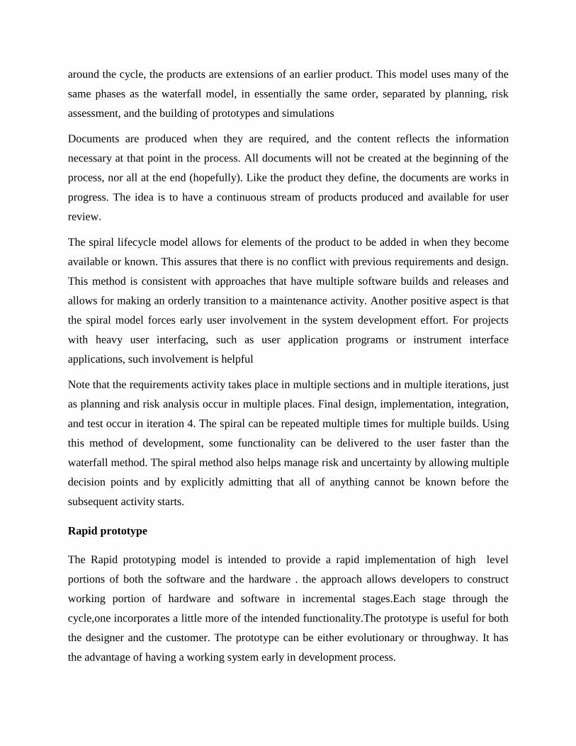
The design process
The design process comprises five distinct stages although it may vary for particular projects or
design disciplines. This information may be useful when working with a designer to understand
the processes involved. Before the project is started however, a vital question has to be asked:
―Why do you need a new identity, brochure or website etc?‖ This question is the key to
undertaking a successful project.
Identifying and formulating the requirement specification
Requirements analysis in systems engineering and software engineering, encompasses those
tasks that go into determining the needs or conditions to meet for a new or altered product, taking
account of the possibly conflicting requirements of the various stakeholders, analyzing,
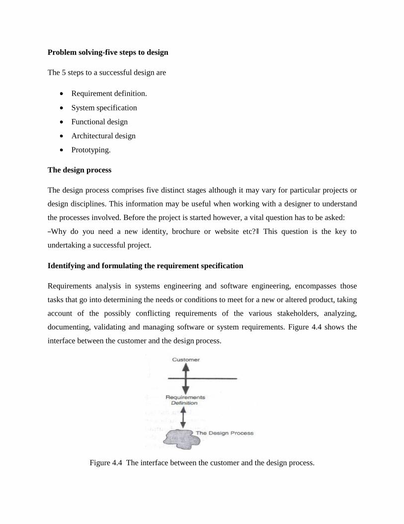
documenting, validating and managing software or system requirements. Figure 4.4 shows the
interface between the customer and the design process.
Figure 4.4 The interface between the customer and the design process.
Requirements analysis is critical to the success of a systems or software project. The
requirements should be documented, actionable, measurable, testable, traceable, related to
identified business needs or opportunities, and defined to a level of detail sufficient for system
design.
Conceptually, requirements analysis includes three types of activities
Eliciting requirements: the task of identifying the various types of requirements from various
sources including project documentation, business process documentation, and stakeholder
interviews. This is sometimes also called requirements gathering.
Analyzing requirements: determining whether the stated requirements are clear, complete,
consistent and unambiguous, and resolving any apparent conflicts.
Recording requirements: Requirements may be documented in various forms, usually
including a summary list and may include natural-language documents, use cases, user
stories, or process specifications.
Characterizing the system
Requirements analysis can be a long and arduous process during which many delicate
psychological skills are involved. New systems change the environment and relationships
between people, so it is important to identify all the stakeholders, take into account all their
needs and ensure they understand the implications of the new systems. Analysts can employ
several techniques to elicit the requirements from the customer. These may include the
development of scenarios, the identification of use cases, the use of workplace observation
or ethnography, holding interviews, or focus groups and creating requirements
lists. Prototyping may be used to develop an example system that can be demonstrated to
stakeholders. Where necessary, the analyst will employ a combination of these methods to
establish the exact requirements of the stakeholders, so that a system that meets the business
needs is produced.
The specification of the external environment should contain the following for each entity:
Name and description of the entity.
For each I/O variable, the following information is available
➢ The name of the signal.
➢ The use of the signal as an i/p or o/p.
➢ The nature of the signal as an event,data,state variable.
Responsibilities-activities.
Relationships.
Safety and reliability.
The system design specification
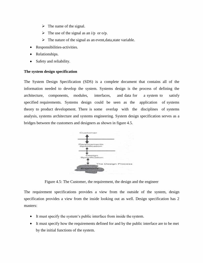
The System Design Specification (SDS) is a complete document that contains all of the
information needed to develop the system. Systems design is the process of defining the
architecture, components, modules, interfaces, and data for a system to satisfy
specified requirements. Systems design could be seen as the application of systems
theory to product development. There is some overlap with the disciplines of systems
analysis, systems architecture and systems engineering. System design specification serves as a
bridges between the customers and designers as shown in figure 4.5.
Figure 4.5: The Customer, the requirement, the design and the engineer
The requirement specifications provides a view from the outside of the system, design
specification provides a view from the inside looking out as well. Design specification has 2
masters:
It must specify the system‘s public interface from inside the system.
It must specify how the requirements defined for and by the public interface are to be met
by the initial functions of the system.
Five areas should be considered are:
Geographical constraints.
Characterization of and constraints on interface signals.
User interface requirements
Temporal constraints.
Electrical infrastructure consideration
Safety and reliability
System specification versus system requirements
➢ Requirements give a description of something wanted or needed. They are a set of needed
properties.
➢ Specification is a description of some entity that has or implements those properties.
A System Requirements Specification is a structured collection of information that embodies the
requirements of a system.
Requirements and specifications are very important components in the development of
any embedded system. Requirements analysis is the first step in the system design process,
where a user's requirements should be clarified and documented to generate the corresponding
specifications. While it is a common tendency for designers to be anxious about starting the
design and implementation, discussing requirements with the customer is vital in the
construction of safety-critical systems. For activities in this first stage has significant impact on
the downstream results in the system life cycle.
For example, errors developed during the requirements and specifications stage may lead
to errors in the design stage. When this error is discovered, the engineers must revisit the
requirements and specifications to fix the problem. This leads not only to more time wasted but
also the possibility of other requirements and specifications errors. Many accidents are traced to
requirements flaws, incomplete implementation of specifications, or wrong assumptions about
the requirements. While these problems may be acceptable in non-safety-critical systems, safety-
critical systems cannot tolerate errors due to requirements and specifications. Therefore, it is
necessary that the requirements are specified correctly to generate clear and accurate
specifications.
There is a distinct difference between requirements and specifications. A requirement is a
condition needed by a user to solve a problem or achieve an objective. A specification is a
document that specifies, in a complete, precise, verifiable manner, the requirements, design,
behavior, or other characteristics of a system, and often, the procedures for determining whether
these provisions have been satisfied. For example, a requirement for a car could be that the
maximum speed to be at least 120mph. The specification for this requirement would include
technical information about specific design aspects. Another term that is commonly seen in
books and papers is requirements specification which is a document that specifies the
requirements for a system or component. It includes functional requirements, performance
requirements, interface requirements, design requirements, and developement standards.
A specification is a precise description of the system that meets stated requirements. A
specification document should be
Complete
Consistent
Comprehensible
Traceable to the requirement
Unambiguous
Modifiable
Able to be written
Functional design
The functional design process maps the "what to do" of the Requirements Specification into the
"how to do it" of the design specifications. During this stage, the overall structure of the product
is defined from a functional viewpoint. The functional design describes the logical system flow,
data organization, system inputs and outputs, processing rules, and operational characteristics of
the product from the user's point of view. The functional design is not concerned with the
software or hardware that will support the operation of the product or the physical organization
of the data or the programs that will accept the input data, execute the processing rules, and
produce the required output.
Functional Design is a paradigm used to simplify the design of hardware and software devices
such as computer software and increasingly, 3D models. A functional design assures that each
modular part of a device has only one responsibility and performs that responsibility with the
minimum of side effects on other parts. Functionally designed modules tend to have
low coupling.
Architectural design
The major objective of the Architectural design activity is the allocation or mapping of the
different pieces of system functionality to the appropriate hardware anf software blocks. Work is
based on the detailed functional structure. The important constraints that must be considered
include items as
The geographical distribution.
Physical and user interfaces
System performance specifications.
Timing constraints and dependability requirements
Power consumption
Legacy components and cost.
Hardware and software specification and design
For the software design, the following must be analyzed and decided.
Whether to use a real time kernel.
Whether several functions can be combined in order to reduce the number of software
tasks and if so, how?
A priority for each task.
An implementation technique for each intertask relationship.
The important criteria that we strive to optimize are
Implementation cost
Development time and cost
Performance and dependability constraints
Power consumption
Size
Functional model versus architectural model
An appropriate model has to include elements both at the functional and architectural level to be
able to represent and evaluate hardware/software system.
Functional model
The functional model describes a system through a set of interacting functional elements. The
design proceeds at a high level without initial bias toward any specific implementation. We have
freedom to explore and to be creative. The functional models will interact using one of the
following 3 types of relations
The shared variable relation-which defines a data exchange without temporal
dependencies.
The synchronization relation- which specifies temporal dependency.
The message transfer by port- which implies a producer/consumer kind of relationship.
Architectural model
Tha architectural model describes the physical architecture of the system based on real
components such as microprocessor, arrayed logics, special purpose processors,analog and
digital components, and the many interconnections between them.
Prototyping
The prototype phase leads to an operational system prototype. A prototype implementation
includes
Detailed design
Debugging

Validation
Testing
A prototype is an early sample or model built to test a concept or process or to act as a thing to
be replicated or learned from. It is a term used in a variety of contexts, including
semantics, design, electronics, and software programming. A prototype is designed to test and
trial a new design to enhance precision by system analysts and users. Prototyping serves to
provide specifications for a real, working system rather than a theoretical one.
In many fields, there is great uncertainty as to whether a new design will actually do what is
desired. New designs often have unexpected problems. A prototype is often used as part of the
product design process to allow engineers and designers the ability to explore design alternatives,
test theories and confirm performance prior to starting production of a new product. Engineers
use their experience to tailor the prototype according to the specific unknowns still present in the
intended design. For example, some prototypes are used to confirm and verify consumer interest
in a proposed design whereas other prototypes will attempt to verify the performance or
suitability of a specific design approach.
In general, an iterative series of prototypes will be designed, constructed and tested as the final
design emerges and is prepared for production. With rare exceptions, multiple iterations of
prototypes are used to progressively refine the design. A common strategy is to design, test,
evaluate and then modify the design based on analysis of the prototype.
In many product development organizations, prototyping specialists are employed - individuals
with specialized skills and training in general fabrication techniques that can help bridge between
theoretical designs and the fabrication of prototypes.
Other Considerations
The 2 additional complementary and concurrent activities that need to be considered are
Capitalization and reuse
Requirement and traceability management.
Capitalization and reuse
Capitalization
Capitalization and reuse are activities that are essential to the contemporary design
process. Proper and efficient exploitation of intellectual properties is very important
.intellectuel properties are designs, often patented,that can be sold to another party to
develop and sell as their product.
Reuse
One of the main purpose of reuse is to help designers shorten the development life cycle.
Component reuse is facilitated in 2 ways: present and future.
To be reused,a component needs to be
Well defined
Properly modularized
In conformance to some interchange standard.
Requirement and traceability management
Requirement traceability
Requirement traceability refers to the ability to follow the life of a requirement in both the
forward and reverse directions through the entire design process and the design. The few
important pieces of informations are
The means for the project manager and the customer to moniter the development
progress.
A path that can be used during the verification and validation of the product against the
original specification.
A means of identifying which hardware or software modules are affected if a requirement
changes.
Requirement management
Requirement management addresses
Requirement specifications
Changes
Improvements
Corrections
During the design, such changes are difficult to avoid for many reasons. Therefore a clear
procedure that facilitates a way to accommodate such modifications has to be used during the
whole design process.
Archiving the project
When the product has finally been released to production, some work remains to be done. If the
product follows the typical life cycle, bugs that must be fixed will be expected and added, and
the next generation product will build on the current. The typical project will have had many
contributors. A basic list can include
Product planning
Design and development
Test
Manufacturing
Marketing
Sales
Each group will have information, knowledge, documentation, and tools that will be important in
future. figure depicts a typical project software directory.
Performance Analysis and Optimization
Performance or efficiency measures
Performance is a measure of the results achieved. Performance efficiency is the ratio
between effort expended and results achieved. The difference between current performance and
the theoretical performance limit is the performance improvement zone.
Another way to think of performance improvement is to see it as improvement in four
potential areas. First, is the resource INPUT requirements (e.g., reduced working capital,
material, replacement/reorder time, and set-up requirements). Second, is the THROUGHPUT
requirements, often viewed as process efficiency; this is measured in terms of time, waste, and
resource utilization. Third, OUTPUT requirements, often viewed from a cost/price, quality,
functionality perspective. Fourth, OUTCOME requirements, did it end up making a difference.
Performance improvement is the concept of measuring the output of a
particular process or procedure, then modifying the process or procedure to increase the output,
increase efficiency, or increase the effectiveness of the process or procedure. The concept of
performance improvement can be applied to either individual performance such as an athlete or
organizational performance such as a racing team or a commercial enterprise.
In Organizational development, performance improvement is the concept of
organizational change in which the managers and governing body of an organization put into
place and manage a program which measures the current level of performance of the
organization and then generates ideas for modifying organizational
behavior and infrastructure which are put into place to achieve higher output. The primary goals
of organizational improvement are to increase organizational effectiveness and efficiency to
improve the ability of the organization to deliver goods and or services. A third area sometimes
targeted for improvement is organizational efficacy, which involves the process of setting
organizational goals and objectives.
Performance improvement at the operational or individual employee level usually
involves processes such as statistical quality control. At the organizational level, performance
improvement usually involves softer forms of measurement such as customer
satisfaction surveys which are used to obtain qualitative information about performance from the
viewpoint of customers.
The difficulty is the significant variability one encounters when running the program.
What input data?
What hardware platform?
What compiler?
What compiler options>
We can focus on several major areas:
Complexity
Time
Power consumption
Memory size
Cost
Weight
Other considerations include
Development time
Ease of maintenance
Extensibility
The following considerations are
Best or minimum case
➢ When referring to time, the emphasis is on measuring the ability to complete a
task. Such a measure is an essential quantity in many real time scheduling
algorithms.
➢ With respect to cost, power or weight, the metric becomes a value below which
one cannot remove any more parts.
➢ With respect to size, one is looking for the smallest amount needed.
Average case
➢ Gives a typical measure; often, this is sufficient.
Worst case
➢ The largest or longest value of a particular measure. When we refer to time, we
are looking at an upper or lower bound on a schedule.
The system
A system is a set of interacting or interdependent components forming an integrated whole[1]
or a
set of elements (often called 'components' ) and relationships which are different from
relationships of the set or its elements to other elements or sets
We consider hardware to comprise
Computational and control elements.
Communication subsystem
Memory
We consider software to be
Algorithms and data structures.
Control and scheduling.
Complexity analysis- A high level measure
Complexity analysis involves breaking down a user task into a set of constituent steps and then
calculating a complexity metric for each step in the task relative to the type of user. Complexity
analysis can also be used to provide relative comparisons of complexity between releases of a
product.
The complexity of an algorithm is a function describing the efficiency of the algorithm in terms
of the amount of data the algorithm must process. Usually there are natural units for the domain
and range of this function. There are two main complexity measures of the efficiency of an
algorithm:
Time complexity is a function describing the amount of time an algorithm takes in terms
of the amount of input to the algorithm. "Time" can mean the number of memory
accesses performed, the number of comparisons between integers, the number of times
some inner loop is executed, or some other natural unit related to the amount of real time
the algorithm will take. We try to keep this idea of time separate from "wall clock" time,
since many factors unrelated to the algorithm itself can affect the real time (like the
language used, type of computing hardware, proficiency of the programmer, optimization
in the compiler, etc.). It turns out that, if we chose the units wisely, all of the other stuff
doesn't matter and we can get an independent measure of the efficiency of the algorithm.
Space complexity is a function describing the amount of memory (space) an algorithm
takes in terms of the amount of input to the algorithm. We often speak of "extra" memory
needed, not counting the memory needed to store the input itself. Again, we use natural
(but fixed-length) units to measure this. We can use bytes, but it's easier to use, say,
number of integers used, number of fixed-sized structures, etc. In the end, the function we
come up with will be independent of the actual number of bytes needed to represent the
unit. Space complexity is sometimes ignored because the space used is minimal and/or
obvious, but sometimes it becomes as important an issue as time.
The methodology
The steps involved in analyzing a complexity of a problem perform trade-off analyses in the
design cycle. They are
Decompose the problem into a set of basic operations.
Count the total number of such operations.
Derive a formula, based in some parameter and that is the size of the problem.
Use order of magnitudes estimation to assess behavior
Analyzing code
As one gains facility in analyzing and understanding the behavior of a system, it becomes
evident rather quickly that even the most complex parts of a system are ultimately composed of
fundamental modules. Let‘s now analyze several of the basic flow of control construct that are
commonly found in many algorithms. The analysis is done from the perspective of time
performance.
Constant Time statements
The execution of constant time statements ,is a constant, independent of the size of the input.
Declarations and initializations of simple data types:
Int x,y;
Char mychar=‘a‘;
Assignment statements of simple data types:
x-y;
Arithmetic operations:
X=5.y+4.z;
Array referencing:
A[j]
Referencing/ dereferencing pointers:
Cursor=head-> next;
Most conditional tests:
If(x<12)….
Looping construct
Looping constructs are a common flow of control mechanism. any loop analysis has 2 parts.
Determine the number of iterations to be performed.
Determine the number of steps per iteration.
For loop
for loop is a programming language statement which allows code to be repeatedly executed.
A for loop is classified as an iteration statement.
or (int i = 0; i < 100; i++) {
/* Prints the numbers 0 to 99, each separated by a space. */
System.out.print(i);
System.out.print(' ');
}
System.out.println();
While loop
a while loop is a control flow statement that allows code to be executed repeatedly based on a
given boolean condition. The while loop can be thought of as a repeating if statement.
int x = 0;
while (x < 5)
{
printf ("x = %d\n", x);
x++;
}
Sequential statements
For a sequence of statements, simply compute their individual complexity functions.
Conditional statements
Conditional statements are features of a programming language which perform different
computations or actions depending on whether a programmer-
specified Boolean condition evaluates to true or false. Apart from the case of branch predication,
this is always achieved by selectively altering the control flow based on some condition.
IF (Boolean condition) THEN
(Consequent)
ELSE
(Alternative)
END IF
When an interpreter finds an If, it expects a Boolean condition – for example, x > 0, which
means "the variable x contains a number that is greater than zero" – and evaluates that condition.
If the condition is true, the statements following the then are executed. Otherwise, the execution
continues in the following branch – either in the else block (which is usually optional), or if there
is no else branch, then after the end If.
After either branch has been executed, control returns to the point after the end If.
Analysis of Algorithms
Efficiency of an algorithm can be measured in terms of:
• Execution time (time complexity)
• The amount of memory required (space complexity)
Time complexity:
For most of the algorithms associated with this course, time complexity comparisons are more
interesting than space complexity comparisons .A measure of the amount of time required to
execute an Factors that should not affect time complexity analysis:
• The programming language chosen to implement the algorithm
• The quality of the compiler
• The speed of the computer on which the algorithm is to be executed algorithm
Time complexity analysis for an algorithm is independent of programming language, machine
used. Objectives of time complexity analysis:
• To determine the feasibility of an algorithm by estimating an upper bound on the amount of
work performed
• To compare different algorithms before deciding on which one to implement.
• Analysis is based on the amount of work done by the algorithm
• Time complexity expresses the relationship between the size of the input and the run time for
the algorithm
• Usually expressed as a proportionality, rather than an exact function
• To simplify analysis, we sometimes ignore work that takes a constant amount of time,
independent of the problem input size
• When comparing two algorithms that perform the same task, we often just
Concentrate on the differences between algorithms
Simplified analysis can be based on:
• Number of arithmetic operations performed
• Number of comparisons made
• Number of times through a critical loop
• Number of array elements accessed
Instructions in detail
It is assumed that a program or algorithm is made up of several common flows of control
constructs. The basic constructs will be analyzed, several additional caveats are in order.
Single thread of execution is assumed.
The analysis is conducted at the assembly language level. Each different compiler is
going to generate somewhat different assembly code, even for the same target. The
analysis must be based on the compiler that is generating the final code for the
microprocessor used in the design.
Compilers support different options for the compilation process. Such variations include
the size of the target memory. Different code may be generated for a small memory
model versus a large memory model.
Consistency is the keyword. always perform the analysis on the code that will ultimately be
embedded in the system being designed.
A hardware interrupt is an electronic alerting signal sent to the processor from an external
device, either a part of the computer itself such as a disk controller or an external peripheral.
For example, pressing a key on the keyboard or moving the mouse triggers hardware
interrupts that cause the processor to read the keystroke or mouse position.
Time ,etc- a more detailed look
Time is one of the most critical constraints that must be considered when designing
embedded system. we must consider both hardware and software timing. On the hardware
side, one must consider the internal delays of the hardware components as well as the delays
through external elements. Software performance is affected by both the path through the
program and the timing of the individual instructions.
Metrics
Response time- the interval between the occurrence of an event and the completion of some
associated action.
Time loading- this is the percentage of time that the CPU is doing useful work.
Memory loading- this is the percentage of usable memory being used.
Response time
Response time is the time a system or functional unit takes to react to a given input. In data
processing, the response time perceived by the end user is the interval between
(a) The instant at which an operator at a terminal enters a request for a response from
a computer.
(b) The instant at which the last character of the response is received at a terminal.
In a data system, the system response time is the interval between the receipt of the end
of transmission of an inquiry message and the beginning of the transmission of a response
message to the station originating the inquiry.
Polled loops
Polled loops are the simplest and the response time consists of three components
Hardware delays in the external device to set the signaling event.
Time to test the flag
Time needed to respond to and process the event associated with the flag.
Co-routine
In a noninterrupt environment, the time for a co-routine may be computed directly or, more
often,bounded, which we compute as the worst case path through each component.
Time loading
Time loading is the percentage of time that the CPU is doing useful work.analyzing time loading
entails the execution times of the constituent modules. These times are computed by finding the
time spent in both the primary tasks and the support tasks. Then compute the ratio of
To compute the times, three primary methods are used:
Instruction counting
Simulation
Physical measurement
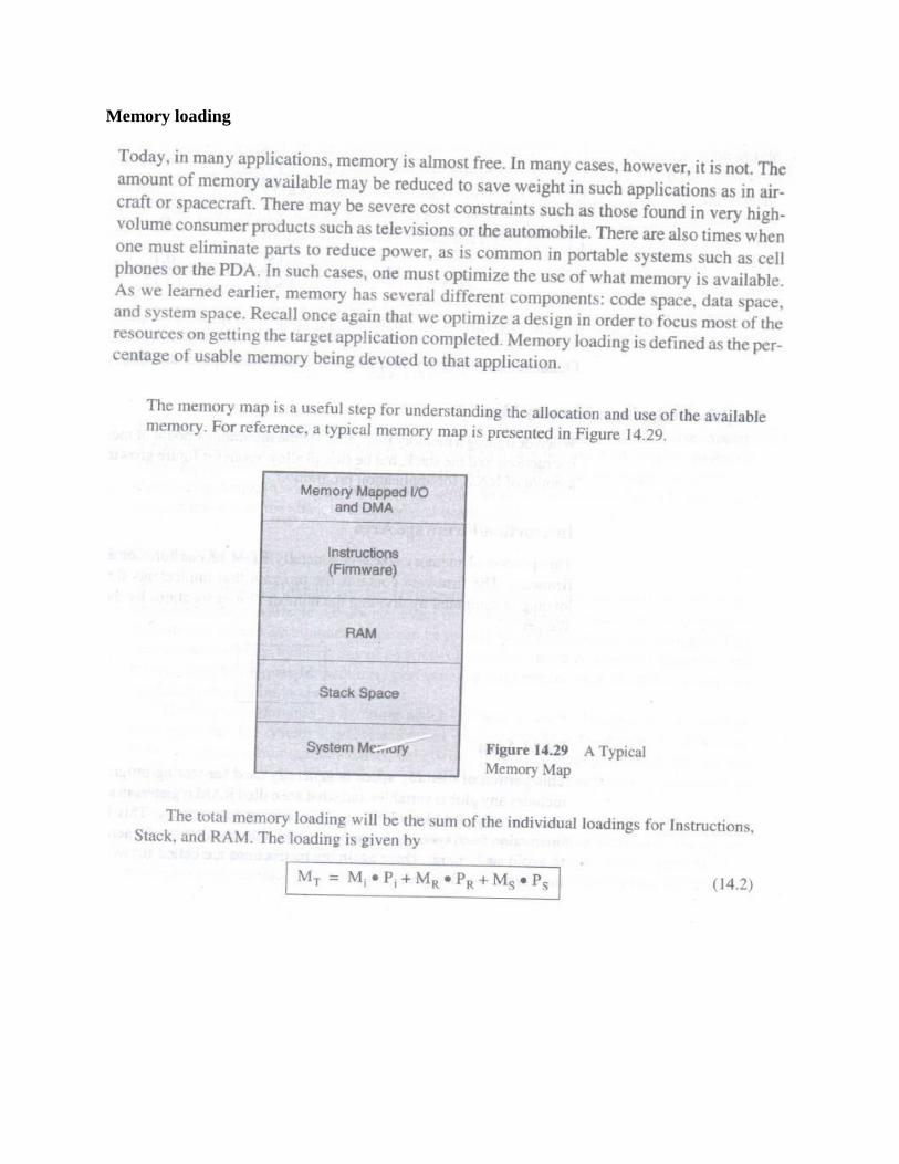
Memory loading
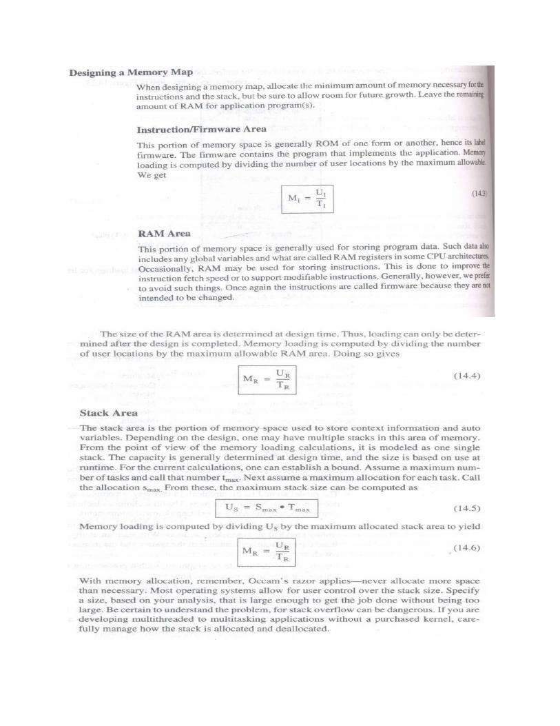
Thoughts on performance optimization
When investigating how to improve the performance of a system, one should think of a few
things. When optimizing, it is important to think about
1. What is being optimized?
2. Why is it being optimized?
3. What will be the effect on the overall program if the module being optimized is
eliminated from the program?
4. Is the optimization appropriate to the operating context?
Performance optimization
In order to improve the performance, we must look at the common mistakes that are often made
when assessing and trying to improve performance
Common mistakes
Expecting improvement in one aspect of the design to improve the overall performance
proportional to improvement.
Using hardware independent metrics to predict performance.
Using peak performance
Comparing performance based on a couple of metrics
Using synthetic benchmarks.
Tricks of the trade
Response time and time loading can be reduced in a number of ways. Here are a couple of
simple ones.
Use lookup tables or combinational logic.
Perform measurements and computations at a rate and significance that is consistent with
the rate of change and values of the data, the type of arithemetic, and the number of
significant digits calculated.
Certain arithemetic calculations can be implemented through shifting operations rather
than using a standard mathematical computation.
Learn from the compiler experts. Compiler writers commonly use many tricks to reduce
code size and to improve speed performance.
Loop management.
Flow of control optimization.
Use registers and caches.
Use only necessary values.
Optimize a common path or frequently used code block. The most frequently used path
or highly used code segment should be the most highly optimized.
Use page mode accesses.
Know when to use recursion vs iteration
Macros and inlining functions.
Hardware accelarators
One technique that can be used to gain significant performance increase with respect to a
software implementation is to move some of the functionality to hardware. Such a collection
of components is called a hardware accelerator. The accelerator is often attatched to the CPU
bus. Communication with the CPU is accomplished through many of the same techniques
that have already been discussed.
Shared variables.
Implemented as data and control registers located in accelerator.
Shared memory locations.
We may use DMA
Hardware accelerators are used when there are functions whose operations do not map well onto
the CPU. Possible examples include
Bit and nit field operations.
Differing precisions of arithmetic calculations.
Very high speed arithmetic
FFT calculations
Multiples
Very high speed or associative search.
High demand input or output operations, with tight timing constraints and high
throughput.
Streaming applications including high speed audio and video. With such application,
delays in the time domain translate directly to distortion in the frequency domain.
Caches and performance
A CPU cache is a cache used by the central processing unit of a computer to reduce the
average time to access memory. The cache is a smaller, faster memory which stores copies of the
data from frequently used main memory locations. As long as most memory accesses are cached
memory locations, the average latency of memory accesses will be closer to the cache latency
than to the latency of main memory.
The proportion of accesses that result in a cache hit is known as the hit rate, and can be a
measure of the effectiveness of the cache for a given program or algorithm.
Read misses delay execution because they require data to be transferred from memory much
more slowly than the cache itself. Write misses may occur without such penalty, since the
processor can continue execution while data is copied to main memory in the background.
Instruction caches are similar to data caches, but the CPU only performs read accesses
(instruction fetches) to the instruction cache. (With Harvard architecture and modified Harvard
architecture CPUs, instruction and data caches can be separated for higher performance, but they
can also be combined to reduce the hardware overhead.)
In computer science, a cache is a component that transparently stores data so that future
requests for that data can be served faster. The data that is stored within a cache might be values
that have been computed earlier or duplicates of original values that are stored elsewhere. If
requested data is contained in the cache (cache hit), this request can be served by simply reading
the cache, which is comparatively faster. Otherwise (cache misses), the data has to be
recomputed or fetched from its original storage location, which is comparatively slower. Hence,

the greater the number of requests that can be served from the cache, the faster the overall system
performance becomes.
To be cost efficient and to enable an efficient use of data, caches are relatively small.
Nevertheless, caches have proven themselves in many areas of computing because access
patterns in typical computer applications have locality of reference. References exhibit temporal
locality if data is requested again that has been recently requested already. References
exhibit spatial locality if data is requested that is physically stored close to data that has been
requested already.
Small memories on or close to the CPU can operate faster than the much larger main memory.
Most CPUs since the 1980s have used one or more caches, and modern high-end embedded,
desktop and server microprocessors may have as many as half a dozen, each specialized for a
specific function. Examples of caches with a specific function are the D-cache and I-cache (data
cache and instruction cache).