Embed Size (px)
Citation preview
1. General description
The EM783-SC/SP/TP/MC3/MC6 is an ARM Cortex-M0-based, low-cost 32-bit family of application processors, designed for energy measurement and monitoring applications. The EM783 offers programmability and on-chip metrology functionality combined with a low power, simple instruction set. It also has memory addressing together with reduced code size compared to existing 8/16-bit architectures.
The EM783 operate at CPU frequencies of up to 48 MHz.
The digital peripherals on the EM783 include:
• 32 kB of flash memory
• 4 kB of EEPROM data memory
• 8 kB of SRAM data memory
• Fast-mode Plus I2C-bus interface
• RS-485/EIA-485 USART
• one SSP controller
• two general-purpose counter/timers
• up to 22 general-purpose I/O pins
A metrology engine with built-in temperature sensor is used for energy measurements. A 10-bit DAC and an internal voltage reference are also available.
2. Features and benefits
System:
ARM Cortex-M0 processor, running at frequencies of up to 48 MHz.
ARM Cortex-M0 built-in Nested Vectored Interrupt Controller (NVIC).
Serial Wire Debug (SWD).
System tick timer.
Memory:
32 kB on-chip flash program memory.
4 kB on-chip EEPROM data memory for energy registers and calibration parameters; byte erasable and byte programmable.
8 kB SRAM data memory.
16 kB boot ROM.
In-System Programming (ISP) for flash and In-Application Programming (IAP) for flash and EEPROM via on-chip bootloader software.
Includes ROM-based 32-bit integer division routines.
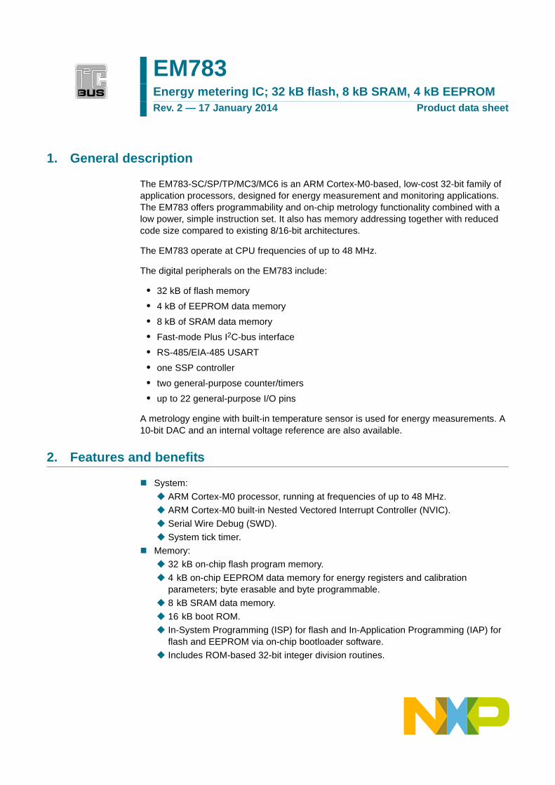
EM783Energy metering IC; 32 kB flash, 8 kB SRAM, 4 kB EEPROMRev. 2 — 17 January 2014 Product data sheet
NXP Semiconductors EM783Energy metering IC; 32 kB flash, 8 kB SRAM, 4 kB EEPROM
Digital peripherals:
Up to 22 General Purpose I/O (GPIO) pins with configurable pull-up/pull-down resistors, repeater mode, and open-drain mode.
Up to 9 pins are configurable with a digital input glitch filter for removing glitches with widths of 10 ns. Two pins are configurable for 20ns glitch filter and another two pins are configurable for 50 ns glitch filters.
GPIO pins can be used as edge and level sensitive interrupt sources.
High-current source output driver (20 mA) on one pin (P0_21).
High-current sink driver (20 mA) on true open-drain pins (P0_2 and P0_3).
Two general-purpose counter/timers with a total of up to four capture inputs and five match outputs.
Programmable Windowed WatchDog Timer (WWDT) with a dedicated, internal low-power WatchDog Oscillator (WDOsc).
Analog peripherals:
Metrology engine for smart metering with one voltage input, one bias input, from two up to six current inputs and a temperature sensor.
Internal voltage reference.
10-bit DAC with flexible conversion triggering.
Serial interfaces:
USART with fractional baud rate generation, internal FIFO, support for RS-485/9-bit mode and synchronous mode.
One SSP controller with FIFO and multi-protocol capabilities.
I2C-bus interface supporting the full I2C-bus specification and Fast-mode Plus with a data rate of 1 Mbit/s with multiple address recognition and monitor mode.
Clock generation:
Crystal Oscillator (SysOsc) with an operating range of 1 MHz to 25 MHz.
12 MHz internal RC Oscillator (IRC) trimmed to 1 % accuracy that can optionally be used as a system clock.
Internal low-power, Low-Frequency Oscillator (LFOsc) with programmable frequency output.
Clock input for external system clock (25 MHz typical).
PLL allows CPU operation up to the maximum CPU rate with the IRC, the external clock, or the SysOsc as clock sources.
Clock output function with divider that can reflect the SysOsc, the IRC, the main clock, or the LFOsc.
Power control:
Supports ARM Cortex-M0 Sleep mode as reduced power mode.
Power profiles residing in boot ROM allowed to optimize performance and minimize power consumption for any given application through one simple function call.
Processor wake-up from reduced power mode using any interrupt.
Power-On Reset (POR).
BrownOut Detect (BOD) with two separate programmable thresholds for interrupt and one hardware controlled reset trip point.
POR and BOD are always enabled for rapid UVLO protection against power supply voltage drops below 2.4 V.
Unique device serial number for identification.
EM783 All information provided in this document is subject to legal disclaimers. © NXP B.V. 2014. All rights reserved.Product data sheet Rev. 2 — 17 January 2014 2 of 58
NXP Semiconductors EM783Energy metering IC; 32 kB flash, 8 kB SRAM, 4 kB EEPROM
Single 3.3 V power supply (2.6 V to 3.6 V).
Temperature range 40 C to +85 C.
Available as a 33-pin HVQFN 7 mm 7 mm 0.85 mm package.
3. Applications
Smart plugs and plug meters
Single phase residential meters
Industrial submeters
Server power monitoring
Smart appliances
4. Ordering information
4.1 Ordering options
Table 1. Ordering information
Type number Package
Name Description Version
EM783-SC HVQFN33 HVQFN: plastic thermal enhanced very thin quad flat package; no leads; 33 terminals; body 7 7 0.85 mm
n/a
EM783-SP HVQFN33 HVQFN: plastic thermal enhanced very thin quad flat package; no leads; 33 terminals; body 7 7 0.85 mm
n/a
EM783-TP HVQFN33 HVQFN: plastic thermal enhanced very thin quad flat package; no leads; 33 terminals; body 7 7 0.85 mm
n/a
EM783-MC3 HVQFN33 HVQFN: plastic thermal enhanced very thin quad flat package; no leads; 33 terminals; body 7 7 0.85 mm
n/a
EM783-MC6 HVQFN33 HVQFN: plastic thermal enhanced very thin quad flat package; no leads; 33 terminals; body 7 7 0.85 mm
n/a
Table 2. Ordering options
Type number Flash SRAM EEPROM Metrology engine inputs
10-bit DAC
USART SSP/SPI
I2C Package
EM783-SC 32 kB 8 kB 4 kB 1x I, 1x V 1 1 1 1 HVQFN33
EM783-SP 32 kB 8 kB 4 kB 2x I, 1x V 1 1 1 1 HVQFN33
EM783-TP 32 kB 8 kB 4 kB 3x I, 3x V 1 1 1 1 HVQFN33
EM783-MC3 32 kB 8 kB 4 kB 3x I, 1x V 1 1 1 1 HVQFN33
EM783-MC6 32 kB 8 kB 4 kB 6x I, 1x V 1 1 1 1 HVQFN33
EM783 All information provided in this document is subject to legal disclaimers. © NXP B.V. 2014. All rights reserved.
Product data sheet Rev. 2 — 17 January 2014 3 of 58
NXP Semiconductors EM783Energy metering IC; 32 kB flash, 8 kB SRAM, 4 kB EEPROM
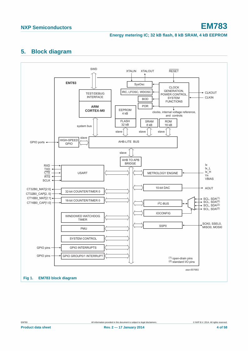
5. Block diagram
Fig 1. EM783 block diagram
SRAM8 kB
ARMCORTEX-M0
TEST/DEBUGINTERFACE
FLASH32 kB
EEPROM4 kB
HIGH-SPEEDGPIO
AHB TO APBBRIDGE
CLOCKGENERATION,
POWER CONTROL,SYSTEM
FUNCTIONS
RESET
clocks, internal voltage reference,and controls
SWD
EM783
aaa-007681
slave
slave
slave
ROM16 kB
slaveslave
AHB-LITE BUSGPIO ports
CLKOUTCLKIN
IRC, LFOSC, WDOSC
SysOsc
POR
BOD
USART
32-bit COUNTER/TIMER 0
IxIx_LIx_HVxVBIAS
AOUT
RXDTXD
RTSCTS
SCLK
PMU
SYSTEM CONTROL
WINDOWED WATCHDOGTIMER
GPIO INTERRUPTS
GPIO GROUP0/1 INTERRUPT
16-bit COUNTER/TIMER 0
CT32B0_MAT[2:0]CT32B0_CAP[2, 0]CT16B0_MAT[2:1]CT16B0_CAP[1:0]
GPIO pins
GPIO pins
10-bit DAC
system bus
SSP0SCK0, SSEL0,MISO0, MOSI0
I2C-BUS
IOCONFIGSCL, SDA(2)
(1) open-drain pins(2) standard I/O pins
SCL, SDA(2)SCL, SDA(1)
SCL, SDA(2)
XTALIN XTALOUT
METROLOGY ENGINE
EM783 All information provided in this document is subject to legal disclaimers. © NXP B.V. 2014. All rights reserved.
Product data sheet Rev. 2 — 17 January 2014 4 of 58
NXP Semiconductors EM783Energy metering IC; 32 kB flash, 8 kB SRAM, 4 kB EEPROM
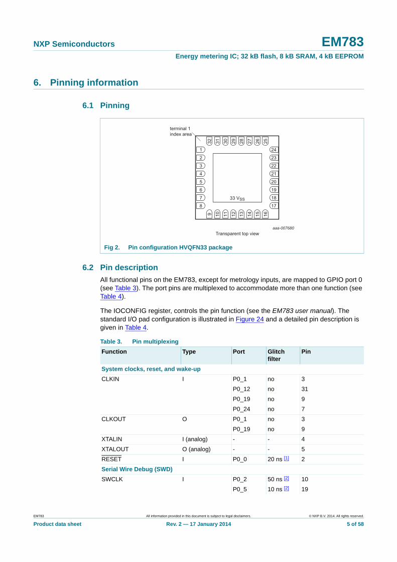
6. Pinning information
6.1 Pinning
6.2 Pin description
All functional pins on the EM783, except for metrology inputs, are mapped to GPIO port 0 (see Table 3). The port pins are multiplexed to accommodate more than one function (see Table 4).
The IOCONFIG register, controls the pin function (see the EM783 user manual). The standard I/O pad configuration is illustrated in Figure 24 and a detailed pin description is given in Table 4.
Fig 2. Pin configuration HVQFN33 package
aaa-007680Transparent top view
8 17
7 18
6 19
5 20
4 21
3 22
2 23
1 24
9 10 11 12 13 14 15 16
32 31 30 29 28 27 26 25
terminal 1index area
33 VSS
Table 3. Pin multiplexing
Function Type Port Glitch filter
Pin
System clocks, reset, and wake-up
CLKIN I P0_1 no 3
P0_12 no 31
P0_19 no 9
P0_24 no 7
CLKOUT O P0_1 no 3
P0_19 no 9
XTALIN I (analog) - - 4
XTALOUT O (analog) - - 5
RESET I P0_0 20 ns [1] 2
Serial Wire Debug (SWD)
SWCLK I P0_2 50 ns [2] 10
P0_5 10 ns [2] 19
EM783 All information provided in this document is subject to legal disclaimers. © NXP B.V. 2014. All rights reserved.
Product data sheet Rev. 2 — 17 January 2014 5 of 58
NXP Semiconductors EM783Energy metering IC; 32 kB flash, 8 kB SRAM, 4 kB EEPROM
SWDIO I/O P0_3 50 ns [2] 11
P0_10 10 ns [2] 25
Metrology engine
V1 I (analog) - no 28
VBIAS I (analog) - no 14
V1 I (analog) - no 22
VBIAS I (analog) - no 23
I1 I (analog) - no 20
I1_L I (analog) - no 20
I1_H I (analog) - no 21
I5 I (analog) - no 21
I2_L I (analog) - no 24
I2 I (analog) - no 24
I2_H I (analog) - no 25
V2 I (analog) - no 25
I6 I (analog) - no 25
I3_L I (analog) - no 26
I3 I (analog) - no 26
I3_H I (analog) - no 27
I4 I (analog) - no 27
V3 I (analog) - no 27
Analog peripherals
AOUT O (analog) P0_4 no 18
ATRG0 I (analog) P0_16 10 ns [2] 13
I2C-bus interface
SCL I/O P0_2 50 ns [2] 10
P0_12 no 31
P0_16 10 ns [2] 13
P0_24 no 7
SDA I/O P0_3 50 ns [2] 11
P0_13 10 ns [2] 32
P0_15 10 ns [2] 27
P0_25 no 12
SSP0 controller
MISO0 I/O P0_22 10 ns [2] 17
MOSI0 I/O P0_4 10 ns [2] 18
P0_19 no 9
SCK0 I/O P0_5 10 ns [2] 19
P0_20 no 15
Table 3. Pin multiplexing …continued
Function Type Port Glitch filter
Pin
EM783 All information provided in this document is subject to legal disclaimers. © NXP B.V. 2014. All rights reserved.
Product data sheet Rev. 2 — 17 January 2014 6 of 58
NXP Semiconductors EM783Energy metering IC; 32 kB flash, 8 kB SRAM, 4 kB EEPROM
[1] Always on.
[2] Programmable on/off. By default, the glitch filter is disabled.
SSEL0 I/O P0_1 no 3
P0_18 no 8
USART
RXD I P0_1 no 3
P0_12 no 31
TXD O P0_13 no 32
P0_15 no 27
P0_26 no 1
SCLK I/O P0_11 10 ns [2] 26
P0_21 no 16
P0_23 no 30
CTS I P0_9 10 ns [2] 24
P0_21 no 16
RTS O P0_10 no 25
P0_23 no 30
16-bit counter/timer CT16B0
CT16B0_CAP0 I P0_2 50 ns [2] 10
P0_18 no 8
CT16B0_CAP1 I P0_16 10 ns [2] 13
CT16B0_MAT1 O P0_4 no 18
P0_9 no 24
CT16B0_MAT2 O P0_5 no 19
P0_10 no 25
32-bit counter/timer CT32B0
CT32B0_CAP0 I P0_11 10 ns [2] 26
P0_23 no 30
CT32B0_CAP2 I P0_15 10 ns [2] 27
P0_26 no 1
CT32B0_MAT0 O P0_12 no 31
CT32B0_MAT1 O P0_13 no 32
CT32B0_MAT2 O P0_1 no 3
Supply and ground pins
VDD(IO) Supply - - 6
VDD(3V3) Supply - - 29
VSS Ground - - 33
VSS(IO) Ground - - 33
Table 3. Pin multiplexing …continued
Function Type Port Glitch filter
Pin
EM783 All information provided in this document is subject to legal disclaimers. © NXP B.V. 2014. All rights reserved.
Product data sheet Rev. 2 — 17 January 2014 7 of 58
NXP Semiconductors EM783Energy metering IC; 32 kB flash, 8 kB SRAM, 4 kB EEPROM
Table 4 shows all pins in order of increasing pin number. The default function after reset is listed first. Port pins P0_0 to P0_26 have internal pull-up resistors enabled after reset except for the true open-drain pins P0_2 and P0_3.
Pull-up/pull-down configuration, repeater, and open-drain modes can be programmed through the IOCONFIG registers for each of the port pins.
Table 4. EM783 pin description
Pin no.
EM783 symbol Type Reset state[1]
Description
SC SP TP MC3 MC6
1 P0_26/TXD/CT32B0_CAP2 [2] I/O I; PU P0_26 — General-purpose digital input/output pin.
O - TXD — Transmitter data output for USART.
I - CT32B0_CAP2 — Capture input 2 for 32-bit timer 0.
2 RESET/P0_0 [3] I I; PU RESET — External reset input with fixed 20 ns glitch filter: A LOW going pulse on this pin resets the device. It causes I/O ports and peripherals to take on their default states and processor execution to begin at address 0.
I/O - P0_0 — General-purpose digital input/output pin.
3 P0_1/RXD/CLKOUT/CT32B0_MAT2/SSEL0/CLKIN
[2] I/O I; PU P0_1 — General-purpose digital input/output pin. A LOW level on this pin during reset starts the ISP command handler.
I - RXD — Receiver data input for USART.
O - CLKOUT — Clock output.
O - CT32B0_MAT2 — Match output 2 for 32-bit timer 0.
I/O - SSEL0 — Slave Select for SSP0.
I - CLKIN — External clock input.
4 XTALIN [4] - - Input to the oscillator circuit and internal clock generator circuits. Input voltage must not exceed 1.8 V.
5 XTALOUT [4] - - Output from the oscillator amplifier.
6 VDD(IO)[5]
[6]- - 3.3 V input/output supply voltage.
7 P0_24/SCL/CLKIN [2] I/O I; PU P0_24 — General-purpose digital input/output pin.
I/O - SCL — I2C-bus clock input/output. This pin is not an I2C-bus open-drain pin[10].
I - CLKIN — External clock input.
8 P0_18/SSEL0/CT16B0_CAP0 [2] I/O I; PU P0_18 — General-purpose digital input/output pin.
I/O - SSEL0 — Slave Select for SSP0.
I - CT16B0_CAP0 — Capture input 0 for 16-bit timer 0.
9 P0_19/CLKIN/CLKOUT/MOSI0 [2] I/O I; PU P0_19 — General-purpose digital input/output pin.
I - CLKIN — External clock input.
O - CLKOUT — Clock output.
I/O - MOSI0 — Master Out Slave In for SSP0.
EM783 All information provided in this document is subject to legal disclaimers. © NXP B.V. 2014. All rights reserved.
Product data sheet Rev. 2 — 17 January 2014 8 of 58
NXP Semiconductors EM783Energy metering IC; 32 kB flash, 8 kB SRAM, 4 kB EEPROM
10 P0_2/SCL/SWCLK/CT16B0_CAP0 [7] I/O I; IA P0_2 — General-purpose digital input/output pin. High-current sink (20 mA) or standard-current sink (4 mA) programmable; true open-drain for all pin functions. Input glitch filter (50 ns) capable.
I/O - SCL — I2C-bus clock (true open-drain) input/output with selectable 50 ns input glitch filter. Input glitch filter (50 ns) capable.
I - SWCLK — Serial Wire Debug Clock (secondary). Input glitch filter (50 ns) capable.
I - CT16B0_CAP0 — Capture input 0 for 16-bit timer 0.
11 P0_3/SDA/SWDIO [7] I/O I; IA P0_3 — General-purpose digital input/output pin. High-current sink (20 mA) or standard-current sink (4 mA) programmable; true open-drain for all pin functions. Input glitch filter (50 ns) capable.
I/O - SDA — I2C-bus data (true open-drain) input/output. Input glitch filter (50 ns) capable.
I/O - SWDIO — Serial Wire Debug I/O (secondary). Input glitch filter (50 ns) capable.
12 P0_25/SDA [2] I/O I; PU P0_25 — General-purpose digital input/output pin.
I/O - SDA — I2C-bus data input/output. This pin is not an I2C-bus open-drain pin[10].
13 P0_16/ATRG0/CT16B0_CAP1/SCL [8] I/O I; PU P0_16 — General-purpose digital input/output pin. Input glitch filter (10 ns) capable.
I - ATRG0 — Conversion trigger for DAC. Input glitch
filter (10 ns) capable.
I - CT16B0_CAP1 — Capture input 1 for 16-bit timer 0. Input glitch filter (10 ns) capable.
I/O - SCL — I2C-bus clock input/output. This pin is not an I2C-bus open-drain pin[10]. Input glitch filter (10 ns) capable.
14 VBIAS [8] I - VBIAS — Bias voltage input for metrology engine.
15 P0_20/SCK0 [2] I/O I; PU P0_20 — General-purpose digital input/output pin.
I/O - SCK0 — Serial clock for SSP0.
16 P0_21/CTS/SCLK [2] I/O I; PU P0_21 — General-purpose digital input/output pin. If configured as output, this pin is a high-current source output driver (20 mA).
I - CTS — Clear To Send input for USART.
I/O - SCLK — Serial clock for USART.
17 P0_22/MISO0 [2] I/O I; PU P0_22 — General-purpose digital input/output pin. Input glitch filter (10 ns) capable.
I/O - MISO0 — Master In Slave Out for SSP0. Input glitch filter (10 ns) capable.
Table 4. EM783 pin description …continued
Pin no.
EM783 symbol Type Reset state[1]
Description
SC SP TP MC3 MC6
EM783 All information provided in this document is subject to legal disclaimers. © NXP B.V. 2014. All rights reserved.
Product data sheet Rev. 2 — 17 January 2014 9 of 58
NXP Semiconductors EM783Energy metering IC; 32 kB flash, 8 kB SRAM, 4 kB EEPROM
18 P0_4/AOUT/CT16B0_MAT1/MOSI0 [9] I/O I; PU P0_4 — General-purpose digital input/output pin. Input glitch filter (10 ns) capable.
O - AOUT — DAC output.
O - CT16B0_MAT1 — Match output 1 for 16-bit timer 0.
I/O - MOSI0 — Master Out Slave In for SSP0. Input glitch filter (10 ns) capable.
19 SWCLK/P0_5/CT16B0_MAT2/SCK0 [8] I I; PU SWCLK — Primary (default) Serial Wire Debug Clock. Input glitch filter (10 ns) capable.
I/O - P0_5 — General-purpose digital input/output pin. Input glitch filter (10 ns) capable.
O - CT16B0_MAT2 — Match output 2 for 16-bit timer 0.
I/O - SCK0 — Serial clock for SSP0. Input glitch filter (10 ns) capable.
20 I1_L I1_L I1 I1_L I1 [9] I - I1_L — Low-gain current input for metrology engine of SC, SP and MC3 variant.
I - I1 — Current input for metrology engine of TP and MC6 variants.
21 I1_H I1_H R I1_H I5 [8] I - I1_H — High-gain current input for metrology engine of SC, SP and MC3 variant.
I - I5 — Current input for metrology engine of MC6 variant.
I I; PU R — Reserved
22 V1 [8] I - V1 — Voltage input for metrology engine.
23 VBIAS [8] I - VBIAS — Bias voltage input for metrology engine.
24 R/P0_9/CT16B0_MAT1/CTS
I2_L I2 I2_L I2 [8] I I; PU R — Reserved
I/O - P0_9 — General-purpose digital input/output pin. Input glitch filter (10 ns) capable.
O - CT16B0_MAT1 — Match output 1 for 16-bit timer 0.
I - CTS — Clear To Send input for USART. Input glitch filter (10 ns) capable.
I - I2_L — Low-gain current input for metrology engine of SP and MC3 variant.
I - I2 — Current input for metrology engine of TP and MC6 variants.
Table 4. EM783 pin description …continued
Pin no.
EM783 symbol Type Reset state[1]
Description
SC SP TP MC3 MC6
EM783 All information provided in this document is subject to legal disclaimers. © NXP B.V. 2014. All rights reserved.
Product data sheet Rev. 2 — 17 January 2014 10 of 58
NXP Semiconductors EM783Energy metering IC; 32 kB flash, 8 kB SRAM, 4 kB EEPROM
25 SWDIO/P0_10/CT16B0MAT2/RTS
I2_H V2 I2_H I6 [8] I/O I; PU SWDIO — Primary (default) Serial Wire Debug I/O. Input glitch filter (10 ns) capable.
I/O - P0_10 — General-purpose digital input/output pin. Input glitch filter (10 ns) capable.
O - CT16B0_MAT2 — Match output 2 for 16-bit timer 0.
O - RTS — Request To Send output for USART.
I - I2_H — High-gain current input for metrology engine of SP and MC3 variant.
I - I6 — Current input for metrology engine of MC6 variant.
I - V2 — Voltage input for metrology engine of TP variant.
26 P0_11/SCLK/CT32B0_CAP0
I3 I3_L I3 [8] I/O I; PU P0_11 — General-purpose digital input/output pin. Input glitch filter (10 ns) capable.
I/O - SCLK — Serial clock for USART. Input glitch filter (10 ns) capable.
I - CT32B0_CAP0 — Capture input 0 for 32-bit timer 0. Input glitch filter (10 ns) capable.
I - I3_L — Low-gain current input for metrology engine of MC3 variant.
I - I3 — Current input for metrology engine of TP and MC6 variants.
27 P0_15/TXD/CT32B0_CAP2/SDA
V3 I3_H I4 [8] I/O I; PU P0_15 — General-purpose digital input/output pin. Input glitch filter (10 ns) capable.
O - TXD — Transmitter data output for USART.
I - CT32B0_CAP2 — Capture input 2 for 32-bit timer 0. Input glitch filter (10 ns) capable.
I/O - SDA — I2C-bus data input/output. This pin is not an I2C-bus open-drain pin[10]. Input glitch filter (10 ns) capable.
I - I3_H — High-gain current input for metrology engine of MC3 variant.
I - I4 — Current input for metrology engine of MC6 variant.
I - V3 — Voltage input for metrology engine of TP variant.
28 V1 [2] I - V1 — Voltage input for metrology engine.
29 VDD(3V3)[5]
[6]- - 3.3 V supply voltage to the metrology engine, internal
regulator, and internal clock generator circuits. Also used as the metrology engine reference voltage.
30 P0_23/RTS/CT32B0_CAP0/SCLK [2] I/O I; PU P0_23 — General-purpose digital input/output pin.
O - RTS — Request To Send output for USART.
I - CT32B0_CAP0 — Capture input 0 for 32-bit timer 0.
I/O - SCLK — Serial clock for USART.
Table 4. EM783 pin description …continued
Pin no.
EM783 symbol Type Reset state[1]
Description
SC SP TP MC3 MC6
EM783 All information provided in this document is subject to legal disclaimers. © NXP B.V. 2014. All rights reserved.
Product data sheet Rev. 2 — 17 January 2014 11 of 58
NXP Semiconductors EM783Energy metering IC; 32 kB flash, 8 kB SRAM, 4 kB EEPROM
[1] Pin state at reset for default function: I = Input; O = Output; PU = internal pull-up resistor (weak PMOS device) enabled; IA = inactive, no pull-up/down enabled.
[2] 5 V tolerant pin providing standard digital I/O functions with configurable modes and configurable hysteresis (Figure 24).
[3] See Figure 25 for the reset configuration.
[4] When the system oscillator is not used, connect XTALIN and XTALOUT as follows: XTALIN can be left floating or can be grounded (grounding is preferred to reduce susceptibility to noise). XTALOUT should be left floating. See Section 12.1 if an external clock is connected to the XTALIN pin.
[5] If separate supplies are used for VDD(3V3) and VDD(IO), ensure that the power supply pins are filtered for noise. Using separate filtered supplies reduces the noise to the metrology engine and analog blocks (see also Section 12.1).
[6] If separate supplies are used for VDD(3V3) and VDD(IO), ensure that the voltage difference between both supplies is smaller than or equal to 0.5 V.
[7] I2C-bus pins compliant with the I2C-bus specification for I2C standard mode, I2C Fast-mode, and I2C Fast-mode Plus.
[8] 5 V tolerant pin providing standard digital I/O functions with configurable modes, configurable hysteresis, and analog I/O. When configured as an analog I/O, digital section of the pin is disabled, and the pin is not 5 V tolerant (Figure 24).
[9] Not a 5 V tolerant pin due to special analog functionality. Pin provides standard digital I/O functions with configurable modes, configurable hysteresis, and analog I/O. When configured as an analog I/O, the digital section of the pin is disabled (Figure 24).
[10] I2C-bus pins are standard digital I/O pins and have limited performance and electrical characteristics compared to the full I2C-bus specification. Pins can be configured with an on-chip pull-up resistor (PMOS device) and with open-drain mode. In this mode, typical bit rates of up to 100 kbit/s with 20 pF load are supported if the internal pull-ups are enabled. Higher bit rates can be achieved with an external resistor.
[11] Thermal pad. Connect to ground.
31 P0_12/RXD/CT32B0_MAT0/SCL/CLKIN [2] I/O I; PU P0_12 — General-purpose digital input/output pin.
I - RXD — Receiver data input for USART.
O - CT32B0_MAT0 — Match output 0 for 32-bit timer 0.
I/O - SCL — I2C-bus clock input/output. This pin is not an I2C-bus open-drain pin [10].
I - CLKIN — External clock input.
32 P0_13/TXD/CT32B0_MAT1/SDA [8] I/O I; PU P0_13 — General-purpose digital input/output pin. Input glitch filter (10 ns) capable.
O - TXD — Transmitter data output for USART.
O - CT32B0_MAT1 — Match output 1 for 32-bit timer 0.
I/O - SDA — I2C-bus data input/output. This pin is not an I2C-bus open-drain pin [10]. Input glitch filter (10 ns) capable.
33 VSS(IO)/VSS - - Ground [11].
Table 4. EM783 pin description …continued
Pin no.
EM783 symbol Type Reset state[1]
Description
SC SP TP MC3 MC6
EM783 All information provided in this document is subject to legal disclaimers. © NXP B.V. 2014. All rights reserved.
Product data sheet Rev. 2 — 17 January 2014 12 of 58
NXP Semiconductors EM783Energy metering IC; 32 kB flash, 8 kB SRAM, 4 kB EEPROM
7. Functional description
7.1 ARM Cortex-M0 processor
The ARM Cortex-M0 is a general purpose, 32-bit microprocessor, which offers high performance and very low power consumption.
7.2 On-chip flash program memory
The EM783 contains up to 32 kB of on-chip flash program memory.
7.3 On-chip EEPROM data memory
The EM783 contains up to 4 kB of on-chip EEPROM data memory.
Remark: The top 64 bytes of the 4 kB EEPROM are reserved and cannot be written to.
7.4 On-chip SRAM
The EM783 contain a total of 8 kB, 4 kB, or 2 kB on-chip static RAM data memory.
7.5 Memory map
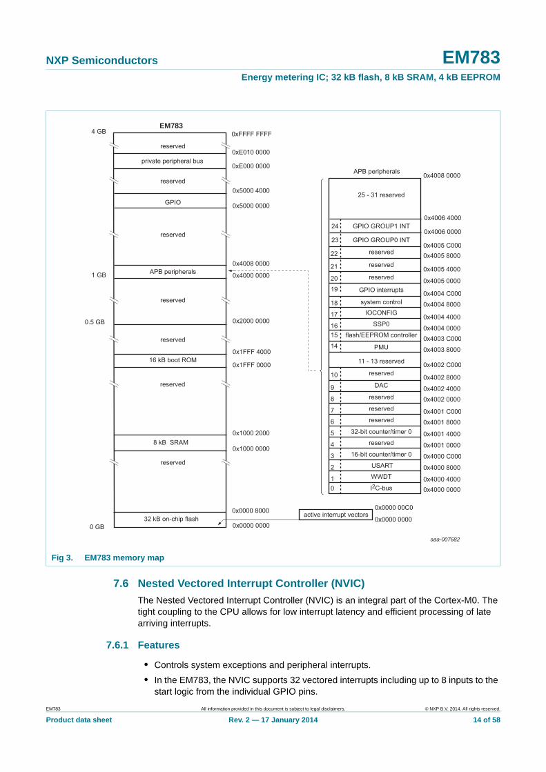
The EM783 incorporate several distinct memory regions, shown in the following figures. Figure 3 shows the overall map of the entire address space from the user program viewpoint following reset. The interrupt vector area supports address remapping.
The AHB peripheral area is 2 MB in size, and is divided to allow for up to 128 peripherals. The APB peripheral area is 512 kB in size and is divided to allow for up to 32 peripherals. Each peripheral of either type is allocated 16 kB of space. This space allows simplifying the address decoding for each peripheral.
EM783 All information provided in this document is subject to legal disclaimers. © NXP B.V. 2014. All rights reserved.
Product data sheet Rev. 2 — 17 January 2014 13 of 58
NXP Semiconductors EM783Energy metering IC; 32 kB flash, 8 kB SRAM, 4 kB EEPROM
7.6 Nested Vectored Interrupt Controller (NVIC)
The Nested Vectored Interrupt Controller (NVIC) is an integral part of the Cortex-M0. The tight coupling to the CPU allows for low interrupt latency and efficient processing of late arriving interrupts.
7.6.1 Features
• Controls system exceptions and peripheral interrupts.
• In the EM783, the NVIC supports 32 vectored interrupts including up to 8 inputs to the start logic from the individual GPIO pins.
Fig 3. EM783 memory map
APB peripherals
0x4000 4000
0x4000 8000
0x4000 C000
0x4001 0000
0x4001 8000
0x4002 0000
0x4002 8000
0x4003 8000
0x4003 C0000x4004 0000
0x4004 4000
0x4004 8000
0x4004 C000
0x4005 80000x4005 C000
0x4008 0000
0x4002 4000
0x4001 C000
0x4001 4000
0x4000 0000
WWDT
32-bit counter/timer 0
USART
PMU
I2C-bus
11 - 13 reserved
DAC
SSP0
reserved
reserved
reserved
reserved
reserved
GPIO interrupts
GPIO GROUP0 INT
reserved
reserved
reserved
25 - 31 reserved
01
2
3
4
5
6
7
8
9
0x4002 C00010
1615
14
17
18
reserved
reserved
0x0000 00000 GB
0.5 GB
4 GB
1 GB
0x1FFF 0000
0x1FFF 4000
0x2000 0000
0x4000 0000
0x4008 0000
0x5000 0000
0x5000 4000
0xFFFF FFFF
reserved
reserved
reserved
APB peripherals
GPIO
0x1000 0000
0x1000 20008 kB SRAM
EM783
16 kB boot ROM
0x0000 0000
0x0000 00C0active interrupt vectors
aaa-007682
reserved
reserved
16-bit counter/timer 0
IOCONFIG
system control
0x4005 0000
0x4005 4000
22
0x4006 000023
GPIO GROUP1 INT0x4006 4000
24
21
19
20
flash/EEPROM controller
0x0000 800032 kB on-chip flash
0xE000 0000
0xE010 0000private peripheral bus
EM783 All information provided in this document is subject to legal disclaimers. © NXP B.V. 2014. All rights reserved.
Product data sheet Rev. 2 — 17 January 2014 14 of 58
NXP Semiconductors EM783Energy metering IC; 32 kB flash, 8 kB SRAM, 4 kB EEPROM
• Four programmable interrupt priority levels with hardware priority level masking.
• Software interrupt generation.
7.6.2 Interrupt sources
Each peripheral device has one interrupt line connected to the NVIC but may have several interrupt flags. Individual interrupt flags may also represent more than one interrupt source.
Up to eight GPIO pins can be programmed to generate an interrupt for a level, and/or a rising edge, and/or a falling edge. The interrupt generating GPIOs can be selected from the GPIO pins with a configurable input glitch filter. The interrupts can be generated regardless of the selected function.
7.7 IOCONFIG block
The IOCONFIG block allows selected pins of the microcontroller to have more than one function. Configuration registers control the multiplexers to allow connection between the pin and the on-chip peripherals.
Peripherals should be connected to the appropriate pins before being activated and prior to any related interrupts being enabled. Activity of any enabled peripheral function that is not mapped to a related pin should be considered undefined.
Up to 9 pins can be configured with a digital input glitch filter for removing voltage glitches with widths of 10 ns (see Table 3 and Table 4). Two pins can be configured with a 20 ns input glitch filter. Another two pins can be configured with a 50 ns digital input glitch filter.
7.8 Fast general-purpose parallel I/O
The GPIO registers control the device pins that are not connected to a specific peripheral function. Pins may be dynamically configured as inputs or outputs. Multiple outputs can be set or cleared in one write operation.
EM783 use accelerated GPIO functions:
• GPIO registers are a dedicated AHB peripheral so that the fastest possible I/O timing can be achieved.
• An entire port value can be written in one instruction.
GPIO pins providing a digital function (maximum 22 pins), can be programmed to generate an interrupt for a level, and/or a rising edge, and/or a falling edge.
7.8.1 Features
• Bit level port registers allow a single instruction to set and clear any number of bits in one write operation.
• Direction control of individual bits.
• All I/O default to inputs with internal pull-up resistors enabled after reset, except for the I2C-bus true open-drain pins P0_2 and P0_3.
• Pull-up/pull-down configuration, repeater, and open-drain modes can be programmed through the IOCONFIG block for each GPIO pin. For the functional diagrams, see Figure 24 and Figure 25.
EM783 All information provided in this document is subject to legal disclaimers. © NXP B.V. 2014. All rights reserved.
Product data sheet Rev. 2 — 17 January 2014 15 of 58
NXP Semiconductors EM783Energy metering IC; 32 kB flash, 8 kB SRAM, 4 kB EEPROM
• Control of the digital output slew rate allowing to switch more outputs simultaneously without degrading the power/ground distribution of the device.
7.9 USART
The EM783 contains one USART.
Support for RS-485/9-bit mode allows both software address detection and automatic address detection using 9-bit mode.
The USART includes a fractional baud rate generator. Standard baud rates such as 115200 Bd can be achieved with any crystal frequency above 2 MHz.
7.9.1 Features
• Maximum USART data bit rate of 3.125 MBit/s.
• 16 byte Receive and Transmit FIFOs.
• Register locations conform to 16C550 industry standard.
• Receiver FIFO trigger points at 1 B, 4 B, 8 B, and 14 B.
• Built-in fractional baud rate generator covering wide range of baud rates without a need for external crystals of particular values.
• FIFO control mechanism that enables software flow control implementation.
• Support for RS-485/9-bit mode.
• Supports a full modem control handshake interface.
• Support for synchronous mode.
7.10 SSP serial I/O controller
The EM783 contains one SSP controller.
The SSP controller can operate on a SPI, 4-wire SSI, or Microwire bus. It can interact with multiple masters and slaves on the bus. Only a single master and a single slave can communicate on the bus during a given data transfer. The SSP supports full-duplex transfers, with frames of 4 bits to 16 bits of data. The data flows from the master to the slave and from the slave to the master. In practice, often only one of the data-flows carries meaningful data.
7.10.1 Features
• Maximum SSP speed of 25 Mbit/s (master) or 4.17 Mbit/s (slave) (in SPI mode).
• Compatible with Motorola SPI, 4-wire Texas Instruments SSI, and National Semiconductor Microwire buses.
• Synchronous serial communication.
• Master or slave operation.
• 8-frame FIFOs for both transmit and receive.
• 4-bit to 16-bit frame.
EM783 All information provided in this document is subject to legal disclaimers. © NXP B.V. 2014. All rights reserved.
Product data sheet Rev. 2 — 17 January 2014 16 of 58
NXP Semiconductors EM783Energy metering IC; 32 kB flash, 8 kB SRAM, 4 kB EEPROM
7.11 I2C-bus serial I/O controller
The EM783 contains one I2C-bus controller.
The I2C-bus is bidirectional for inter-IC control using only two wires: a serial clock line (SCL) and a serial data line (SDA). A unique address recognizes each device which can operate as either a receiver-only device (e.g., an LCD driver) or a transmitter with the capability to both receive and send information (such as memory). Transmitters and/or receivers can operate in either master or slave mode, depending on whether the chip has to initiate a data transfer or is only addressed. The I2C is a multi-master bus that can be controlled by more than one bus master connected to it.
7.11.1 Features
• The I2C-interface is a standard I2C-bus compliant interface with open-drain pins (P0_2 and P0_3). The I2C-bus interface also supports Fast-mode Plus with bit rates up to 1 Mbit/s.
• The true open-drain pins P0_2 and P0_3 can be configured with a 50 ns digital input glitch filter.
• If the true open-drain pins are used for other purposes, a limited-performance I2C-bus interface can be configured from a choice of six GPIO pins. The six GPIO pins are configured in open-drain mode and with a pull-up resistor. In this mode, typical bit rates of up to 100 kbit/s with 20 pF load are supported if the internal pull-ups are enabled. Higher bit rates can be achieved with an external resistor.
• Easy to configure as master, slave, or master/slave.
• Fail-safe operation. When the power to an I2C-bus device is switched off, the SDA and SCL pins connected to the I2C-bus are floating and do not disturb the bus.
• Programmable clocks allow versatile rate control.
• Bidirectional data transfer between masters and slaves.
• Multi-master bus (no central master).
• Arbitration between simultaneously transmitting masters without corruption of serial data on the bus.
• Serial clock synchronization allows devices with different bit rates to communicate via one serial bus.
• Serial clock synchronization can be used as a handshake mechanism to suspend and resume serial transfer.
• The I2C-bus can be used for test and diagnostic purposes.
• The I2C-bus controller supports multiple address recognition and a bus monitor mode.
7.12 Metrology engine
The EM783 contains a metrology engine designed to collect voltage and current inputs. It uses these inputs to calculate the active power, reactive power, apparent power and power factor of a load. The purpose of the metrology engine is for billing and non-billing applications such as plug meters, smart appliances, industrial and consumer submeters.
EM783 All information provided in this document is subject to legal disclaimers. © NXP B.V. 2014. All rights reserved.
Product data sheet Rev. 2 — 17 January 2014 17 of 58
NXP Semiconductors EM783Energy metering IC; 32 kB flash, 8 kB SRAM, 4 kB EEPROM
7.12.1 Features
• Up to 1.0 % accurate for scalable input sources. It maintains this accuracy with a factor of 1 to 1000 down from the maximum current.
• Automatically calculates:
– Vrms
– Irms
– active power in W
– reactive power in VAR
– apparent power in VA
– power factor
– fundamental reactive power in VAR
– fundamental apparent power in VA
– fundamental power factor
– non-fundamental apparent power
– non-active power
– total harmonic distortion of the current
– mains frequency
– CPU core temperature
• Standard API for initializing, starting, stopping and reading data from the metrology engine using the ARM Cortex-M0.
• Temperature measurement supporting temperature compensation. The temperature sensor has a maximum error of 3 degrees C over the ambient temperature range of 40 C to +85 C.
• Very accurate mains frequency measurement.
• Mains frequency operating range of 45 Hz to 65 Hz.
• EEPROM can be used for energy registers and calibration parameters.
• Measurements and active power according to IEC 62053-21.
7.13 10-bit DAC
The DAC allows generation of a variable, rail-to-rail analog output.
7.13.1 Features
• 10-bit DAC.
• Resistor string architecture.
• Buffered output.
• Power-down mode.
• Conversion speed controlled via a programmable bias current.
• Optional output update modes:
– write operations to the DAC register.
EM783 All information provided in this document is subject to legal disclaimers. © NXP B.V. 2014. All rights reserved.
Product data sheet Rev. 2 — 17 January 2014 18 of 58
NXP Semiconductors EM783Energy metering IC; 32 kB flash, 8 kB SRAM, 4 kB EEPROM
– a transition of pin ATRG0. Input signal must be held for a minimum of three system clock periods.
– a timer match signal.
• If the DAC is not powered down, it holds the output value during Sleep mode.
7.14 Internal voltage reference
The internal voltage reference is an accurate 0.9 V and is the output of a low voltage band gap circuit. A typical value at Tamb = 25 C is 0.903 V. This value varies typically only 3 mV over the 0 C to 85 C temperature range (see Table 21 and Figure 21).
7.15 General-purpose external event counter/timers
The EM783 includes one 32-bit counter/timer and one 16-bit counter/timer. The counter/timer is designed to count cycles of the system derived clock. It can optionally generate interrupts or perform other actions at specified timer values, based on four match registers. Each counter/timer also includes four capture inputs to trap the timer value when an input signal transitions, optionally generating an interrupt.
7.15.1 Features
• A 32-bit/16-bit timer/counter with a programmable 32-bit/16-bit prescaler.
• Counter or timer operation.
• Four capture channels per timer, that can take a snapshot of the timer value when an input signal transitions. A capture event may also generate an interrupt. Up to three capture channels are pinned out.
• Four match registers per timer that allow:
– Continuous operation with optional interrupt generation on match.
– Stop timer on match with optional interrupt generation.
– Reset timer on match with optional interrupt generation.
• Up to four external outputs corresponding to match registers, with the following capabilities:
– Set LOW on match.
– Set HIGH on match.
– Toggle on match.
– Do nothing on match.
7.16 System tick timer
The ARM Cortex-M0 includes a system tick timer (SYSTICK) that is intended to generate a dedicated SYSTICK exception at a fixed time interval (typically 10 ms).
7.17 Windowed WatchDog Timer (WWDT)
If software fails to service the controller periodically within a programmable time window, the purpose of the watchdog is to reset it.
EM783 All information provided in this document is subject to legal disclaimers. © NXP B.V. 2014. All rights reserved.
Product data sheet Rev. 2 — 17 January 2014 19 of 58
NXP Semiconductors EM783Energy metering IC; 32 kB flash, 8 kB SRAM, 4 kB EEPROM
7.17.1 Features
• Internally resets chip if not periodically reloaded during the programmable time-out period.
• Optional windowed operation requires reload to occur between a minimum and maximum time period, both programmable.
• Optional warning interrupt can be generated at a programmable time before a watchdog time-out.
• Enabled by software but requires a hardware reset or a watchdog reset/interrupt to be disabled.
• If enabled, an incorrect feed sequence causes a reset or interrupt.
• Flag to indicate watchdog reset.
• Programmable 24-bit timer with internal prescaler.
• Selectable time period from (Tcy(WDCLK) 256 4) to (Tcy(WDCLK) 224 4) in multiples of Tcy(WDCLK) 4.
• The WatchDog Clock (WDCLK) source can be selected from the internal RC oscillator (IRC), or the dedicated watchdog oscillator (WDOsc). This gives a wide range of potential timing choices of watchdog operation under different power conditions.
7.18 Clocking and power control
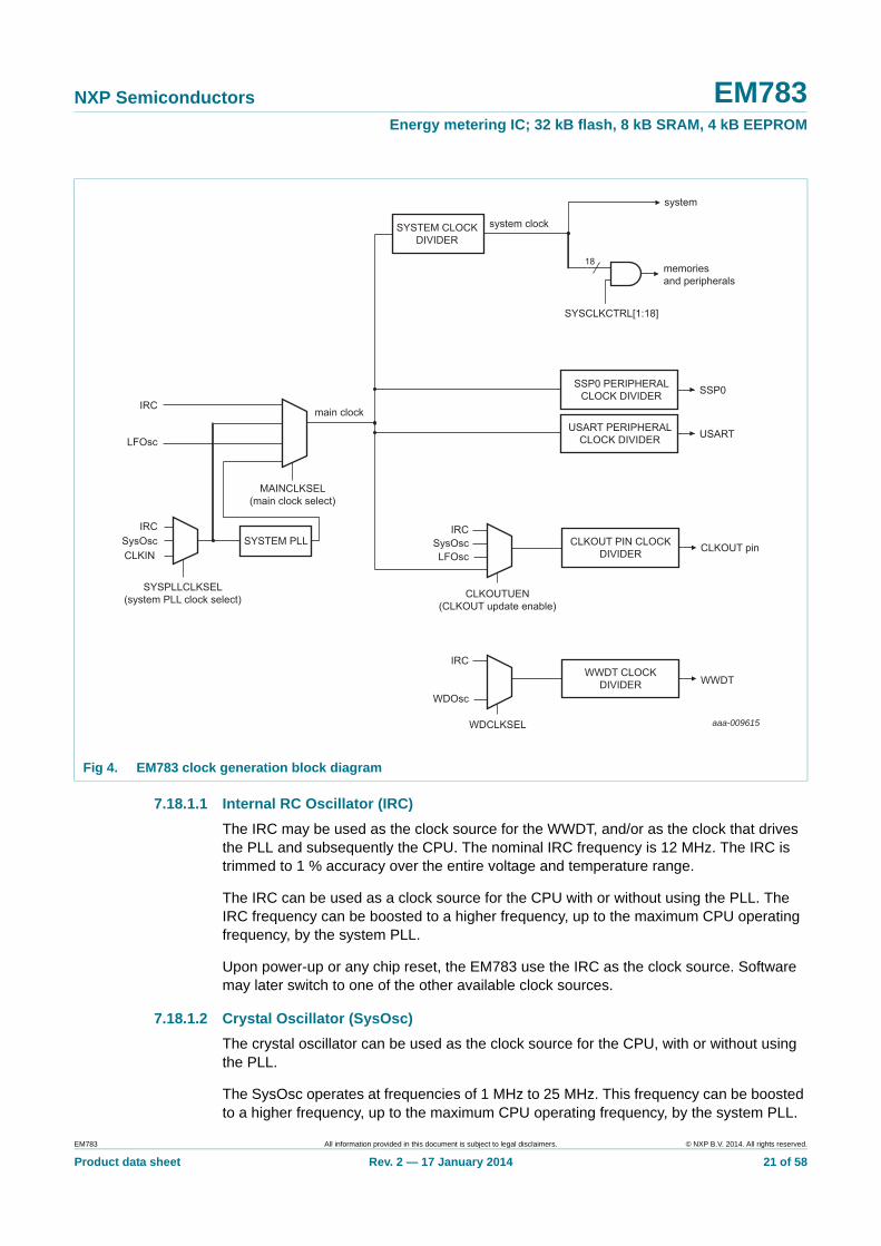
7.18.1 Crystal and internal oscillators
The EM783 include four independent oscillators.
1. The crystal oscillator (SysOsc) operating at frequencies between 1 MHz and 25 MHz.
2. The internal RC Oscillator (IRC) with a fixed frequency of 12 MHz, trimmed to 1 % accuracy.
3. The internal low-power, Low-Frequency Oscillator (LFOsc) with a programmable nominal frequency between 9.4 kHz and 2.3 MHz with 40 % accuracy.
4. The dedicated WatchDog Oscillator (WDOsc) with a programmable nominal frequency between 9.4 kHz and 2.3 MHz with 40 % accuracy.
Each oscillator, except the WDOsc, can be used for more than one purpose as required in a particular application.
Following reset, the EM783 operates from the IRC until switched by software. This allows systems to operate without any external crystal and the bootloader code to operate at a known frequency.
See Figure 4 for an overview of the EM783 clock generation.
EM783 All information provided in this document is subject to legal disclaimers. © NXP B.V. 2014. All rights reserved.
Product data sheet Rev. 2 — 17 January 2014 20 of 58
NXP Semiconductors EM783Energy metering IC; 32 kB flash, 8 kB SRAM, 4 kB EEPROM
7.18.1.1 Internal RC Oscillator (IRC)
The IRC may be used as the clock source for the WWDT, and/or as the clock that drives the PLL and subsequently the CPU. The nominal IRC frequency is 12 MHz. The IRC is trimmed to 1 % accuracy over the entire voltage and temperature range.
The IRC can be used as a clock source for the CPU with or without using the PLL. The IRC frequency can be boosted to a higher frequency, up to the maximum CPU operating frequency, by the system PLL.
Upon power-up or any chip reset, the EM783 use the IRC as the clock source. Software may later switch to one of the other available clock sources.
7.18.1.2 Crystal Oscillator (SysOsc)
The crystal oscillator can be used as the clock source for the CPU, with or without using the PLL.
The SysOsc operates at frequencies of 1 MHz to 25 MHz. This frequency can be boosted to a higher frequency, up to the maximum CPU operating frequency, by the system PLL.
Fig 4. EM783 clock generation block diagram
aaa-009615
SYSTEM PLLIRC
SysOsc
WDOsc
IRC
LFOsc
MAINCLKSEL(main clock select)
SYSPLLCLKSEL(system PLL clock select)
SYSTEM CLOCKDIVIDER
system
SYSCLKCTRL[1:18]
memoriesand peripherals
SSP0 PERIPHERALCLOCK DIVIDER SSP0
USART PERIPHERALCLOCK DIVIDER USART
WWDT CLOCKDIVIDER WWDT
WDCLKSEL
LFOsc
IRCSysOsc CLKOUT PIN CLOCK
DIVIDER CLKOUT pin
CLKOUTUEN(CLKOUT update enable)
main clock
system clock
IRC
18
CLKIN
EM783 All information provided in this document is subject to legal disclaimers. © NXP B.V. 2014. All rights reserved.
Product data sheet Rev. 2 — 17 January 2014 21 of 58
NXP Semiconductors EM783Energy metering IC; 32 kB flash, 8 kB SRAM, 4 kB EEPROM
7.18.1.3 Internal Low-Frequency Oscillator (LFOsc) and WatchDog Oscillator (WDOsc)
The LFOsc and the WDOsc are identical internal oscillators. The nominal frequency is programmable between 9.4 kHz and 2.3 MHz. The frequency spread over silicon process variations is 40 %.
The WDOsc is a dedicated oscillator for the windowed WWDT.
The LFOsc can be used as a clock source that directly drives the CPU or the CLKOUT pin.
7.18.2 Clock input
A 3.3 V external clock source (25 MHz typical) can be supplied on the selected CLKIN pin. A 1.8 V external clock source can be supplied on the XTALIN pin (see Section 12.1).
7.18.3 System PLL
The PLL accepts an input clock frequency in the range of 10 MHz to 25 MHz. The input frequency is multiplied up to a high frequency with a Current Controlled Oscillator (CCO). The multiplier can be an integer value from 1 to 32. The CCO operates in the range of 156 MHz to 320 MHz. There is an additional divider in the loop to keep the CCO within its frequency range while the PLL is providing the desired output frequency. The output divider may be set to divide by 2, 4, 8, or 16 to produce the output clock. Since the minimum output divider value is 2, it is insured that the PLL output has a 50 % duty cycle. Software can enable the PLL and it is turned off and bypassed following a chip reset. The program must configure and activate the PLL, wait for the PLL to lock, and then connect to the PLL as a clock source. The PLL settling time is 100 s.
7.18.4 Clock output
The EM783 features a clock output function that routes the IRC, the SysOsc, the LFOsc, or the main clock to an output pin.
7.18.5 Wake-up process
The EM783 begin operation at power-up and when awakened from Deep power-down mode by using the IRC as the clock source. This allows chip operation to resume quickly. If the application requires the SysOsc, the external clock source, or the PLL, software must enable these features. Before using them as a clock source, wait for them to stabilize.
7.18.6 Power control
The EM783 supports the ARM Cortex-M0 Sleep mode. The CPU clock rate may also be controlled as needed by changing clock sources, reconfiguring PLL values, and/or altering the CPU clock divider value. This control allows a trade-off of power versus processing speed based on application requirements. In addition, a register is provided for shutting down the clocks to individual on-chip peripherals. The clock control allows fine-tuning of power consumption. It eliminates all dynamic power use in any peripherals that are not required for the application. Selected peripherals have their own clock divider which provides even better power control.
7.18.6.1 Sleep mode
When Sleep mode is entered, the clock to the core is stopped. Resumption from the Sleep mode does not need any special sequence but re-enabling the clock to the ARM core.
EM783 All information provided in this document is subject to legal disclaimers. © NXP B.V. 2014. All rights reserved.
Product data sheet Rev. 2 — 17 January 2014 22 of 58
NXP Semiconductors EM783Energy metering IC; 32 kB flash, 8 kB SRAM, 4 kB EEPROM
In Sleep mode, execution of instructions is suspended until either a reset or interrupt occurs. Peripheral functions continue operation during Sleep mode and may generate interrupts to cause the processor to resume execution. Sleep mode eliminates dynamic power used by the processor itself, memory systems and related controllers, and internal buses.
7.18.6.2 Power profiles
The power consumption in Active and Sleep modes can be optimized for the application through simple calls to the power profile. The power configuration routine configures the EM783 for one of the following power modes:
• Power mode 0: Default mode corresponding to power configuration after reset.
• Power mode 1: CPU performance mode corresponding to optimized processing capability.
• Power mode 2: Efficiency mode corresponding to optimized balance of current consumption and CPU performance.
• Power mode 3: Low-current mode corresponding to lowest power consumption.
In addition, the power profile includes routines to select the optimal PLL settings for a given system clock and PLL input clock.
7.19 System control
7.19.1 UnderVoltage LockOut (UVLO) protection
See Section 10.1 “Power supply fluctuations” for details on the settling times of the BOD and POR circuits. These circuits constitute the UVLO protection.
7.19.2 Reset
Reset has four sources on the EM783: the RESET pin, the WatchDog reset, power-on reset (POR), the ARM SYSRESETREQ software request and the BrownOut Detection (BOD) circuit. The RESET pin is a Schmitt trigger input pin and uses a special pad (see Figure 25). Assertion of chip reset by any source (after the operating voltage attains a usable level) starts the IRC and initializes the flash controller. After the BOD and the POR resets are released, the internal reset timer counts for 100 s until the internal reset is removed.
When the internal Reset is removed, the processor begins executing at address 0, which is initially the Reset vector mapped from the boot block. At that point, all of the processor and peripheral registers have been initialized to predetermined values.
Writing to a special function register allows the software to reset peripherals such as the I2C-bus interface, USART, SSP controller, counter/timers and DAC.
EM783 All information provided in this document is subject to legal disclaimers. © NXP B.V. 2014. All rights reserved.
Product data sheet Rev. 2 — 17 January 2014 23 of 58
NXP Semiconductors EM783Energy metering IC; 32 kB flash, 8 kB SRAM, 4 kB EEPROM
7.19.3 Brownout detection
The EM783 includes two programmable levels for monitoring the voltage on the VDD(3V3) pin. If this voltage falls below one of the four selected levels, the BOD asserts an interrupt signal to the NVIC. To cause a CPU interrupt, this signal is enabled for interrupt in the Interrupt Enable Register in the NVIC. Software can monitor the signal by reading a dedicated status register. In addition, the BOD circuit supports one hardware controlled voltage level for triggering a chip reset.
7.19.4 Code security (Code Read Protection - CRP)
This feature of the EM783, allows different levels of security to be enabled in the system. It is used to restrict access to the on-chip flash and use of the Serial Wire Debugger (SWD) and In-System-Programming (ISP). When needed, CRP is invoked by programming a specific pattern into a dedicated flash location. The CRP does not affect IAP commands.
In addition, ISP entry via the P0_1 pin can be disabled without enabling CRP. Refer to the EM783 user manual for specific details.
There are three levels of Code Read Protection:
1. CRP1 disables access to the chip via the SWD and allows partial flash update (excluding flash sector 0) using a limited set of the ISP commands. This mode is useful when CRP is required and flash field updates are needed but all sectors cannot be erased.
2. CRP2 disables access to the chip via the SWD and only allows full flash erase and update using a reduced set of the ISP commands.
3. Running an application with level CRP3 selected fully disables any access to the chip via the SWD pins and the ISP. This mode effectively disables ISP override using P0_1 pin. To enable flash update via the USART, the user application must provide a flash update mechanism using IAP calls or call reinvoke ISP command.
In addition to the three CRP levels, sampling of pin P0_1 for valid user code can be disabled. Refer to the EM783 user manual for specific details.
7.19.5 APB interface
The APB peripherals are located on one APB bus.
7.19.6 AHBLite
The AHBLite connects the CPU bus of the ARM Cortex-M0 to the flash memory, the main static RAM, and the Boot ROM.
7.19.7 External interrupt inputs
All GPIO pins can be level or edge sensitive interrupt inputs.
CAUTION
If level three Code Read Protection (CRP3) is selected, no future factory testing can be performed on the device.
EM783 All information provided in this document is subject to legal disclaimers. © NXP B.V. 2014. All rights reserved.
Product data sheet Rev. 2 — 17 January 2014 24 of 58
NXP Semiconductors EM783Energy metering IC; 32 kB flash, 8 kB SRAM, 4 kB EEPROM
7.20 Emulation and debugging
Debug functions are integrated into the ARM Cortex-M0. Serial Wire Debug (SWD) with four breakpoints and two watchpoints is supported.
8. Limiting values
[1] The following applies to the limiting values:
a) This product includes circuitry specifically designed for the protection of its internal devices from the damaging effects of excessive static charge. Nonetheless, it is suggested that conventional precautions be taken to avoid applying greater than the rated maximum.
b) Parameters are valid over operating temperature range unless otherwise specified. All voltages relate to VSS unless otherwise noted.
[2] Maximum/minimum voltage above the maximum operating voltage (see Table 6) and below ground that can be applied for a short time (< 10 ms) to a device without leading to irrecoverable failure. Failure includes the loss of reliability and shorter lifetime of the device.
[3] Applies to all 5 V tolerant I/O pins except true open-drain pins P0_2 and P0_3 and except the 3 V tolerant pins P0_4 and P0_5.
[4] Including the voltage on outputs in 3-state mode.
[5] VDD(IO) present or not present. Compliant with the I2C-bus standard. 5.5 V can be applied to this pin when VDD(IO) is powered down.
[6] Applies to 3 V tolerant pins P0_4 and P0_5.
Table 5. Limiting valuesIn accordance with the Absolute Maximum Rating System (IEC 60134).[1]
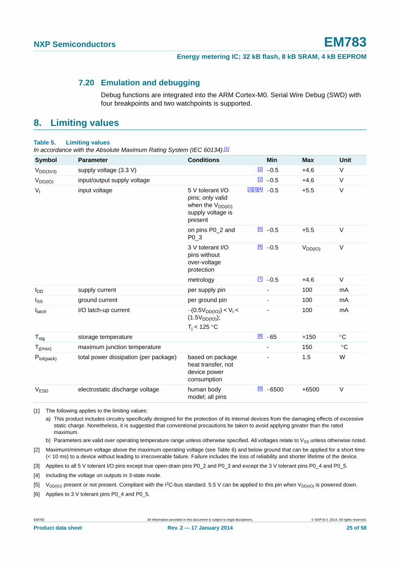
Symbol Parameter Conditions Min Max Unit
VDD(3V3) supply voltage (3.3 V) [2] 0.5 +4.6 V
VDD(IO) input/output supply voltage [2] 0.5 +4.6 V
VI input voltage 5 V tolerant I/O pins; only valid when the VDD(IO) supply voltage is present
[2][3][4] 0.5 +5.5 V
on pins P0_2 and P0_3
[5] 0.5 +5.5 V
3 V tolerant I/O pins without over-voltage protection
[6] 0.5 VDD(IO) V
metrology [7] 0.5 +4.6 V
IDD supply current per supply pin - 100 mA
ISS ground current per ground pin - 100 mA
Ilatch I/O latch-up current (0.5VDD(IO)) < VI < (1.5VDD(IO));
Tj < 125 C
- 100 mA
Tstg storage temperature [8] 65 +150 C
Tj(max) maximum junction temperature - 150 C
Ptot(pack) total power dissipation (per package) based on package heat transfer, not device power consumption
- 1.5 W
VESD electrostatic discharge voltage human body model; all pins
[9] 6500 +6500 V
EM783 All information provided in this document is subject to legal disclaimers. © NXP B.V. 2014. All rights reserved.
Product data sheet Rev. 2 — 17 January 2014 25 of 58
NXP Semiconductors EM783Energy metering IC; 32 kB flash, 8 kB SRAM, 4 kB EEPROM
[7] A Metrology engine input voltage above 3.6 V can be applied for a short time without leading to immediate, unrecoverable failure. Accumulated exposure to elevated voltages at 4.6 V must be less than 10^6 s total over the lifetime of the device. Applying an elevated voltage to the metrology engine inputs for a long time affects the reliability of the device and reduces its lifetime.
[8] Dependent on package type.
[9] Human body model: equivalent to discharging a 100 pF capacitor through a 1.5 k series resistor.
9. Static characteristics
Table 6. Static characteristicsTamb = 40 C to +85 C, unless otherwise specified.
Symbol Parameter Conditions Min Typ[1] Max Unit
VDD(3V3) supply voltage (3.3 V) 2.6 3.3 3.6 V
VDD(IO) input/output supply voltage
2.6 3.3 3.6 V
IDD supply current Active mode; code
while(1){}
executed from flash; VDD(3V3) = VDD(IO) = 3.3 V; low-current mode (see Section 7.18.6.2)
system clock = 12 MHz; all peripherals disabled
[2][4][5] - 3 - mA
system clock = 48 MHz; all peripherals disabled
[2][6][5] - 8 - mA
Sleep mode; system clock = 12 MHz; VDD(3V3) = VDD(IO) = 3.3 V; power mode 0 (see Section 7.18.6.2)
all peripherals disabled; 12 MHz
[2][4][5] - 2 - mA
all peripherals disabled; 48 MHz
[2][4][5] - 5 - mA
Standard port pins, RESET
IIL LOW-level input current VI = 0 V; on-chip pull-up resistor disabled
- 0.5 1000 nA
IIH HIGH-level input current
VI = VDD(IO); on-chip pull-down resistor disabled
- 0.5 1000 nA
IOZ OFF-state output current
VO = 0 V; VO = VDD(IO); on-chip pull-up/down resistors disabled
- 0.5 1000 nA
VI input voltage pin configured to provide a digital function
5 V tolerant pins
[7][8] 0 - 5.0 V
3 V tolerant pins:P0_4 and P0_5
[7][8] VDD(IO)
VO output voltage output active 0 - VDD(IO) V
VIH HIGH-level input voltage
0.7VDD(IO) - - V
EM783 All information provided in this document is subject to legal disclaimers. © NXP B.V. 2014. All rights reserved.
Product data sheet Rev. 2 — 17 January 2014 26 of 58
NXP Semiconductors EM783Energy metering IC; 32 kB flash, 8 kB SRAM, 4 kB EEPROM
VIL LOW-level input voltage - - 0.3VDD(IO) V
Vhys hysteresis voltage 3.0 V VDD(IO) 3.6 V 0.4 - - V
VOH HIGH-level output voltage
2.6 V VDD(IO) 3.6 V; IOH = 4 mA
0.85VDD(IO) - - V
VOL LOW-level output voltage
2.6 V VDD(IO) 3.6 V; IOL = 4 mA
- - 0.15VDD(IO) V
IOH HIGH-level output current
VOH = VDD(IO) 0.4 V;
2.6 V VDD(IO) 3.6 V
4 - - mA
IOL LOW-level output current
VOL = 0.4 V
2.6 V VDD(IO) 3.6 V
4 - - mA
IOHS HIGH-level short-circuit output current
VOH = 0 V [9] - - 45 mA
IOLS LOW-level short-circuit output current
VOL = VDD(IO)[9] - - 50 mA
Ipd pull-down current VI = 5 V [10] 10 50 150 A
Ipu pull-up current VI = 0 V;
2.6 V VDD(IO) 3.6 V
15 50 85 A
VDD(IO) < VI < 5 V 0 0 0 A
High-drive output pin (P0_21)
IIL LOW-level input current VI = 0 V; on-chip pull-up resistor disabled
- 0.5 10 nA
IIH HIGH-level input current
VI = VDD(IO); on-chip pull-down resistor disabled
- 0.5 10 nA
IOZ OFF-state output current
VO = 0 V; VO = VDD(IO); on-chip pull-up/down resistors disabled
- 0.5 10 nA
VI input voltage pin configured to provide a digital function
[7][8] 0 - 5.0 V
VO output voltage output active 0 - VDD(IO) V
VIH HIGH-level input voltage
0.7VDD(IO) - - V
VIL LOW-level input voltage - - 0.3VDD(IO) V
Vhys hysteresis voltage 0.4 - - V
VOH HIGH-level output voltage
2.6 V VDD(IO) 3.6 V; IOH = 20 mA
VDD(IO) 0.4
- - V
2.6 V VDD(IO) 2.5 V; IOH = 12 mA
VDD(IO) 0.4
- - V
VOL LOW-level output voltage
2.6 V VDD(IO) 3.6 V; IOL = 4 mA
- - 0.4 V
IOH HIGH-level output current
VOH = VDD(IO) 0.4 V;
2.6 V VDD(IO) 3.6 V
20 - - mA
Table 6. Static characteristics …continuedTamb = 40 C to +85 C, unless otherwise specified.
Symbol Parameter Conditions Min Typ[1] Max Unit
EM783 All information provided in this document is subject to legal disclaimers. © NXP B.V. 2014. All rights reserved.
Product data sheet Rev. 2 — 17 January 2014 27 of 58
NXP Semiconductors EM783Energy metering IC; 32 kB flash, 8 kB SRAM, 4 kB EEPROM
[1] Typical ratings are not guaranteed. The values listed are at room temperature (25 C), nominal supply voltages.
[2] Tamb = 25 C.
[3] IDD measurements were performed with all pins configured as GPIO outputs driven LOW and pull-up resistors disabled.
[4] IRC enabled; SysOsc disabled; system PLL disabled.
[5] All digital peripherals disabled in the SYSCLKCTRL register except ROM, RAM, and flash. Peripheral clocks to USART and SSP0/1 disabled in system configuration block. Analog peripherals disabled in the PDRUNCFG register except flash memory.
[6] IRC disabled; SysOsc enabled; system PLL enabled.
[7] Including voltage on outputs in 3-state mode.
[8] All supply voltages must be present.
[9] Allowed as long as the current limit does not exceed the maximum current allowed by the device.
[10] Does not apply to 3 V tolerant pins P0_4.
[11] To VSS.
IOL LOW-level output current
VOL = 0.4 V
2.6 V VDD(IO) 3.6 V
4 - - mA
IOHS HIGH-level short-circuit output current
VOH = 0 V [9] - - 160 mA
IOLS LOW-level short-circuit output current
VOL = VDD(IO)[9] - - 50 mA
Ipd pull-down current VI = 5 V 10 50 150 A
Ipu pull-up current VI = 0 V
2.6 V VDD(IO) 3.6 V
15 50 85 A
VDD(IO) < VI < 5 V 0 0 0 A
I2C-bus pins (P0_2 and P0_3)
VIH HIGH-level input voltage
0.7VDD(IO) - - V
VIL LOW-level input voltage - - 0.3VDD(IO) V
Vhys hysteresis voltage - 0.05VDD(IO) - V
IOL LOW-level output current
VOL = 0.4 V; I2C-bus pins configured as standard mode pins
2.6 V VDD(IO) 3.6 V
4 - - mA
IOL LOW-level output current
VOL = 0.4 V; I2C-bus pins configured as high-current sink pins
2.6 V VDD(IO) 3.6 V
20 - - mA
ILI input leakage current VI = VDD(IO)[11] - 2 4 A
VI = 5 V - 10 22 A
Oscillator pins
Vi(xtal) crystal input voltage 0.5 1.8 1.95 V
Vo(xtal) crystal output voltage 0.5 1.8 1.95 V
Table 6. Static characteristics …continuedTamb = 40 C to +85 C, unless otherwise specified.
Symbol Parameter Conditions Min Typ[1] Max Unit
EM783 All information provided in this document is subject to legal disclaimers. © NXP B.V. 2014. All rights reserved.
Product data sheet Rev. 2 — 17 January 2014 28 of 58
NXP Semiconductors EM783Energy metering IC; 32 kB flash, 8 kB SRAM, 4 kB EEPROM
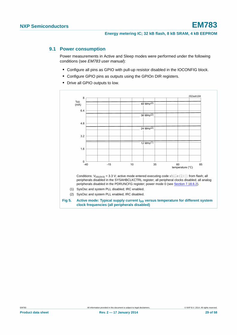
9.1 Power consumption
Power measurements in Active and Sleep modes were performed under the following conditions (see EM783 user manual):
• Configure all pins as GPIO with pull-up resistor disabled in the IOCONFIG block.
• Configure GPIO pins as outputs using the GPIOn DIR registers.
• Drive all GPIO outputs to low.
Conditions: VDD(3V3) = 3.3 V; active mode entered executing code while(1){} from flash; all peripherals disabled in the SYSAHBCLKCTRL register; all peripheral clocks disabled; all analog peripherals disabled in the PDRUNCFG register; power mode 0 (see Section 7.18.6.2).
(1) SysOsc and system PLL disabled; IRC enabled.
(2) SysOsc and system PLL enabled; IRC disabled.
Fig 5. Active mode: Typical supply current IDD versus temperature for different system clock frequencies (all peripherals disabled)
002aah184
-40 -15 10 35 60 850
1.6
3.2
4.8
6.4
8
temperature (°C)
IDD(mA)
12 MHz(1)
24 MHz(2)
36 MHz(2)
48 MHz(2)
EM783 All information provided in this document is subject to legal disclaimers. © NXP B.V. 2014. All rights reserved.
Product data sheet Rev. 2 — 17 January 2014 29 of 58
NXP Semiconductors EM783Energy metering IC; 32 kB flash, 8 kB SRAM, 4 kB EEPROM
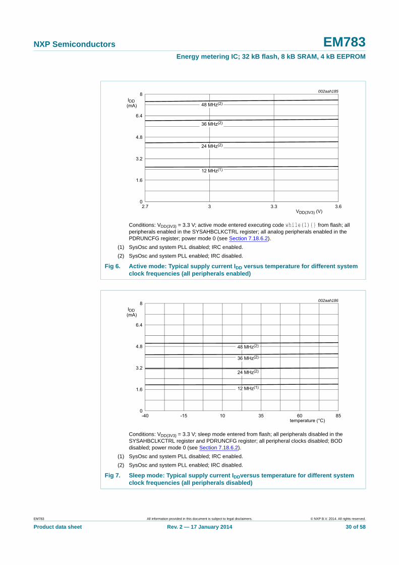
Conditions: VDD(3V3) = 3.3 V; active mode entered executing code while(1){} from flash; all peripherals enabled in the SYSAHBCLKCTRL register; all analog peripherals enabled in the PDRUNCFG register; power mode 0 (see Section 7.18.6.2).
(1) SysOsc and system PLL disabled; IRC enabled.
(2) SysOsc and system PLL enabled; IRC disabled.
Fig 6. Active mode: Typical supply current IDD versus temperature for different system clock frequencies (all peripherals enabled)
Conditions: VDD(3V3) = 3.3 V; sleep mode entered from flash; all peripherals disabled in the SYSAHBCLKCTRL register and PDRUNCFG register; all peripheral clocks disabled; BOD disabled; power mode 0 (see Section 7.18.6.2).
(1) SysOsc and system PLL disabled; IRC enabled.
(2) SysOsc and system PLL enabled; IRC disabled.
Fig 7. Sleep mode: Typical supply current IDDversus temperature for different system clock frequencies (all peripherals disabled)
002aah185
2.7 3 3.3 3.60
1.6
3.2
4.8
6.4
8
VDD(3V3) (V)
IDD(mA)
12 MHz(1)
24 MHz(2)
36 MHz(2)
48 MHz(2)
002aah186
-40 -15 10 35 60 850
1.6
3.2
4.8
6.4
8
temperature (°C)
IDD(mA)
12 MHz(1)
24 MHz(2)
36 MHz(2)
48 MHz(2)
EM783 All information provided in this document is subject to legal disclaimers. © NXP B.V. 2014. All rights reserved.
Product data sheet Rev. 2 — 17 January 2014 30 of 58
NXP Semiconductors EM783Energy metering IC; 32 kB flash, 8 kB SRAM, 4 kB EEPROM
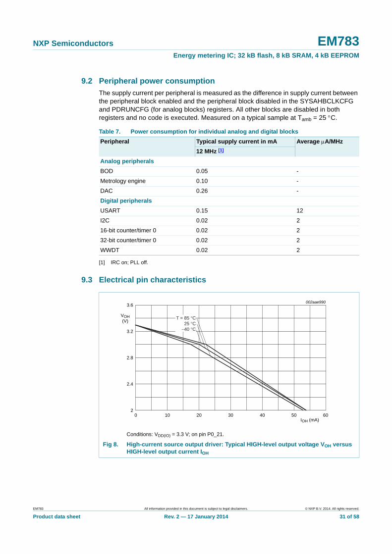
9.2 Peripheral power consumption
The supply current per peripheral is measured as the difference in supply current between the peripheral block enabled and the peripheral block disabled in the SYSAHBCLKCFG and PDRUNCFG (for analog blocks) registers. All other blocks are disabled in both registers and no code is executed. Measured on a typical sample at Tamb = 25 C.
[1] IRC on; PLL off.
9.3 Electrical pin characteristics
Table 7. Power consumption for individual analog and digital blocks
Peripheral
Typical supply current in mA Average A/MHz
12 MHz [1]
Analog peripherals
BOD 0.05 -
Metrology engine 0.10 -
DAC 0.26 -
Digital peripherals
USART 0.15 12
I2C 0.02 2
16-bit counter/timer 0 0.02 2
32-bit counter/timer 0 0.02 2
WWDT 0.02 2
Conditions: VDD(IO) = 3.3 V; on pin P0_21.
Fig 8. High-current source output driver: Typical HIGH-level output voltage VOH versus HIGH-level output current IOH
IOH (mA)0 60402010 5030
002aae990
2.8
2.4
3.2
3.6
VOH(V)
2
T = 85 °C25 °C
−40 °C
EM783 All information provided in this document is subject to legal disclaimers. © NXP B.V. 2014. All rights reserved.
Product data sheet Rev. 2 — 17 January 2014 31 of 58
NXP Semiconductors EM783Energy metering IC; 32 kB flash, 8 kB SRAM, 4 kB EEPROM
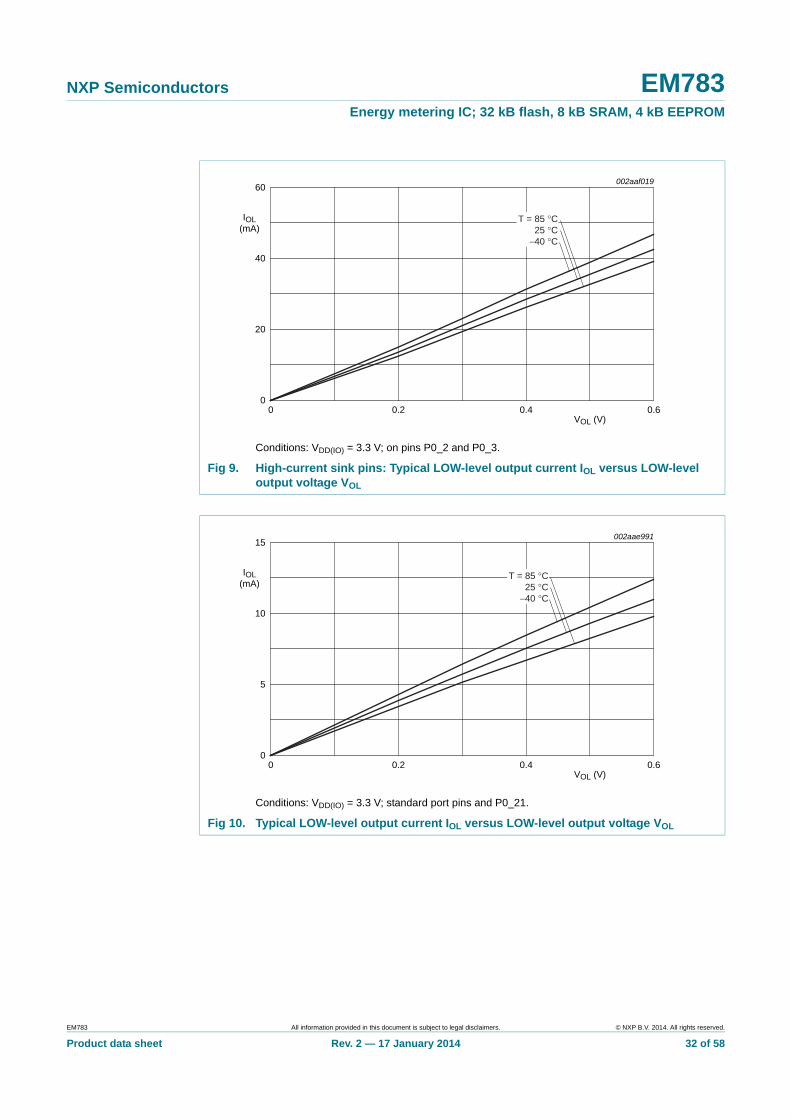
Conditions: VDD(IO) = 3.3 V; on pins P0_2 and P0_3.
Fig 9. High-current sink pins: Typical LOW-level output current IOL versus LOW-level output voltage VOL
Conditions: VDD(IO) = 3.3 V; standard port pins and P0_21.
Fig 10. Typical LOW-level output current IOL versus LOW-level output voltage VOL
VOL (V)0 0.60.40.2
002aaf019
20
40
60
IOL(mA)
0
T = 85 °C25 °C
−40 °C
VOL (V)0 0.60.40.2
002aae991
5
10
15
IOL(mA)
0
T = 85 °C25 °C
−40 °C
EM783 All information provided in this document is subject to legal disclaimers. © NXP B.V. 2014. All rights reserved.
Product data sheet Rev. 2 — 17 January 2014 32 of 58
NXP Semiconductors EM783Energy metering IC; 32 kB flash, 8 kB SRAM, 4 kB EEPROM
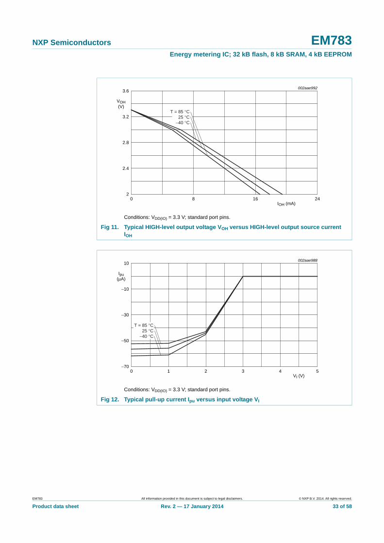
Conditions: VDD(IO) = 3.3 V; standard port pins.
Fig 11. Typical HIGH-level output voltage VOH versus HIGH-level output source current IOH
Conditions: VDD(IO) = 3.3 V; standard port pins.
Fig 12. Typical pull-up current Ipu versus input voltage VI
IOH (mA)0 24168
002aae992
2.8
2.4
3.2
3.6
VOH(V)
2
T = 85 °C25 °C
−40 °C
VI (V)0 542 31
002aae988
−30
−50
−10
10
Ipu(μA)
−70
T = 85 °C25 °C
−40 °C
EM783 All information provided in this document is subject to legal disclaimers. © NXP B.V. 2014. All rights reserved.
Product data sheet Rev. 2 — 17 January 2014 33 of 58
NXP Semiconductors EM783Energy metering IC; 32 kB flash, 8 kB SRAM, 4 kB EEPROM
Conditions: VDD(IO) = 3.3 V; standard port pins.
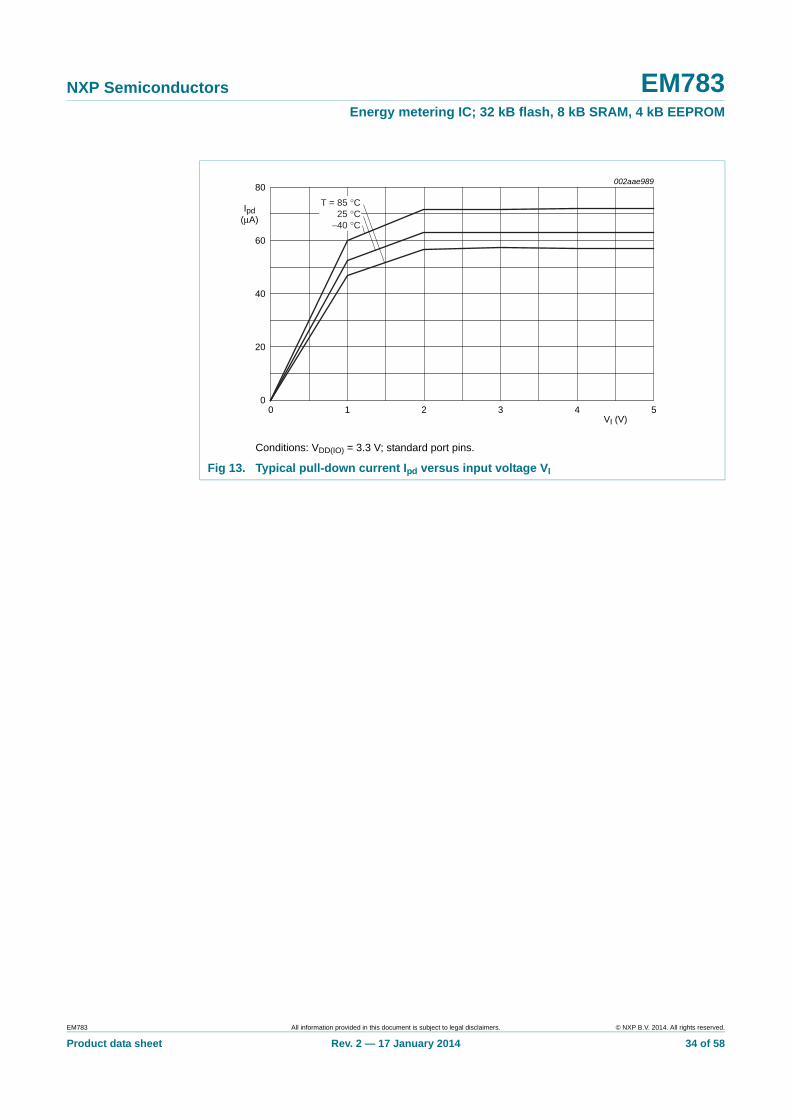
Fig 13. Typical pull-down current Ipd versus input voltage VI
VI (V)0 542 31
002aae989
40
20
60
80
Ipd(μA)
0
T = 85 °C25 °C
−40 °C
EM783 All information provided in this document is subject to legal disclaimers. © NXP B.V. 2014. All rights reserved.
Product data sheet Rev. 2 — 17 January 2014 34 of 58
NXP Semiconductors EM783Energy metering IC; 32 kB flash, 8 kB SRAM, 4 kB EEPROM
10. Dynamic characteristics
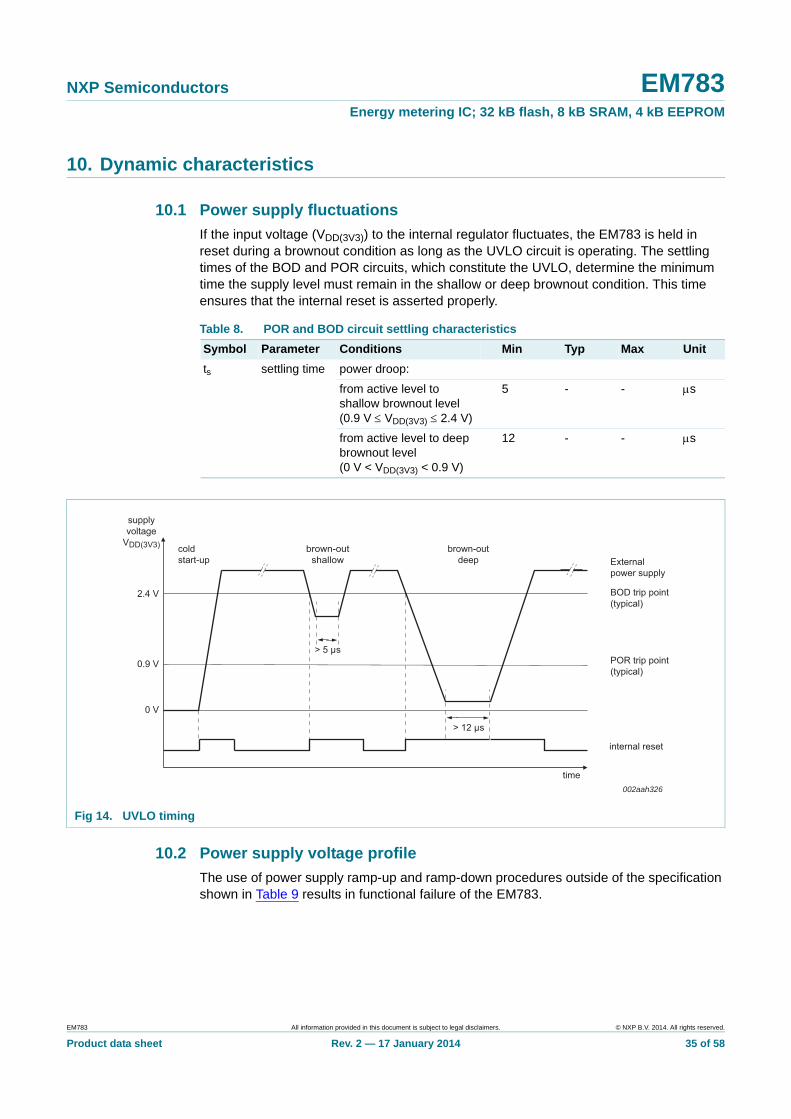
10.1 Power supply fluctuations
If the input voltage (VDD(3V3)) to the internal regulator fluctuates, the EM783 is held in reset during a brownout condition as long as the UVLO circuit is operating. The settling times of the BOD and POR circuits, which constitute the UVLO, determine the minimum time the supply level must remain in the shallow or deep brownout condition. This time ensures that the internal reset is asserted properly.
10.2 Power supply voltage profile
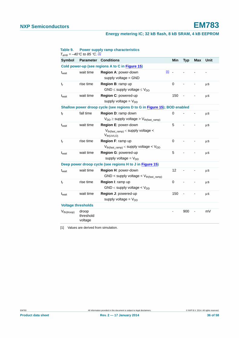
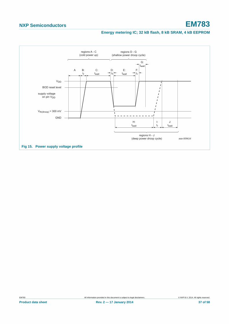
The use of power supply ramp-up and ramp-down procedures outside of the specification shown in Table 9 results in functional failure of the EM783.
Table 8. POR and BOD circuit settling characteristics
Symbol Parameter Conditions Min Typ Max Unit
ts settling time power droop:
from active level to shallow brownout level (0.9 V VDD(3V3) 2.4 V)
5 - - s
from active level to deep brownout level (0 V < VDD(3V3) < 0.9 V)
12 - - s
Fig 14. UVLO timing
Externalpower supply
BOD trip point(typical)
POR trip point(typical)
internal reset
time
brown-outshallow
brown-outdeep
supplyvoltage
VDD(3V3)
2.4 V
0.9 V
0 V
coldstart-up
> 5 μs
> 12 μs
002aah326
EM783 All information provided in this document is subject to legal disclaimers. © NXP B.V. 2014. All rights reserved.
Product data sheet Rev. 2 — 17 January 2014 35 of 58
NXP Semiconductors EM783Energy metering IC; 32 kB flash, 8 kB SRAM, 4 kB EEPROM
[1] Values are derived from simulation.
Table 9. Power supply ramp characteristics Tamb = –40C to 85C. [1]
Symbol Parameter Conditions Min Typ Max Unit
Cold power-up (see regions A to C in Figure 15)
twait wait time Region A: power-down
supply voltage = GND
[1] - - - -
tr rise time Region B: ramp up
GND supply voltage VDD
0 - - s
twait wait time Region C: powered-up
supply voltage = VDD
150 - - s
Shallow power droop cycle (see regions D to G in Figure 15); BOD enabled
tf fall time Region D: ramp down
VDD supply voltage > Vth(fast_ramp)
0 - - s
twait wait time Region E: power-down
Vth(fast_ramp) supply voltage < Vth(UVLO)
5 - - s
tr rise time Region F: ramp up
Vth(fast_ramp) supply voltage < VDD
0 - - s
twait wait time Region G: powered-up
supply voltage = VDD
5 - - s
Deep power droop cycle (see regions H to J in Figure 15)
twait wait time Region H: power-down
GND < supply voltage < Vth(fast_ramp)
12 - - s
tr rise time Region I: ramp up
GND supply voltage < VDD
0 - - s
twait wait time Region J: powered-up
supply voltage = VDD
150 - - s
Voltage thresholds
Vth(droop) droop threshold voltage
- 900 - mV
EM783 All information provided in this document is subject to legal disclaimers. © NXP B.V. 2014. All rights reserved.
Product data sheet Rev. 2 — 17 January 2014 36 of 58
NXP Semiconductors EM783Energy metering IC; 32 kB flash, 8 kB SRAM, 4 kB EEPROM
Fig 15. Power supply voltage profile
A B:tr
F:tr
G:twait
C:twait
E:twait
D:tf
H:twait
J:twait
I:tr
GND
Vth(droop) = 300 mV
VDD
BOD reset level
supply voltageon pin VDD
regions D - G(shallow power droop cycle)
regions H - J(deep power droop cycle)
regions A - C(cold power up)
aaa-009616
EM783 All information provided in this document is subject to legal disclaimers. © NXP B.V. 2014. All rights reserved.
Product data sheet Rev. 2 — 17 January 2014 37 of 58
NXP Semiconductors EM783Energy metering IC; 32 kB flash, 8 kB SRAM, 4 kB EEPROM
10.3 Flash/EEPROM memory
[1] Number of program/erase cycles.
[2] Programming times are given for writing 256 bytes to the flash. Data must be written to the flash in blocks of 256 bytes. Flash programming is accomplished via IAP calls (see EM783 user manual). Execution time of IAP calls depends on the system clock and is typically between 1.5 ms and 2 ms per 256 bytes.
10.4 External clock for oscillator in slave mode
Remark: The input voltage on the XTALIN pin must be 1.95 V (see Table 6). For connecting the oscillator to the XTALIN/XTALOUT pins, see Section 12.1.
[1] Parameters are valid over operating temperature range unless otherwise specified.
[2] Typical ratings are not guaranteed. The values listed are at room temperature (25 C), nominal supply voltages.
Table 10. Flash characteristicsTamb = 40 C to +85 C. Based on JEDEC NVM qualification. Failure rate < 10 ppm for parts as specified below.
Symbol Parameter Conditions Min Typ Max Unit
Nendu endurance [1] 10000 100000 - cycles
tret retention time powered 10 20 - years
unpowered 20 40 - years
ter erase time sector or multiple consecutive sectors
95 100 105 ms
tprog programming time
[2] 0.95 1 1.05 ms
Table 11. EEPROM characteristicsTamb = 40 C to +85 C; VDD(3V3) = 2.6 V to 3.6 V. Based on JEDEC NVM qualification. Failure rate < 10 ppm for parts as specified below.
Symbol Parameter Conditions Min Typ Max Unit
Nendu endurance 100000 1000000 - cycles
tret retention time powered 100 200 - years
unpowered 150 300 - years
ter erase time 64 bytes - 1.8 - ms
tprog programming time
64 bytes - 1.1 - ms
Table 12. Dynamic characteristic: external clock (XTALIN or CLKIN pin)Tamb = 40 C to +85 C; VDD(3V3) over specified ranges.[1]
Symbol Parameter Conditions Min Typ[2] Max Unit
fosc oscillator frequency 1 - 25 MHz
tcy(clk) clock cycle time 40 - 1000 ns
tCHCX clock HIGH time tcy(clk) 0.4 - - ns
tCLCX clock LOW time tcy(clk) 0.4 - - ns
tCLCH clock rise time - - 5 ns
tCHCL clock fall time - - 5 ns
EM783 All information provided in this document is subject to legal disclaimers. © NXP B.V. 2014. All rights reserved.
Product data sheet Rev. 2 — 17 January 2014 38 of 58
NXP Semiconductors EM783Energy metering IC; 32 kB flash, 8 kB SRAM, 4 kB EEPROM
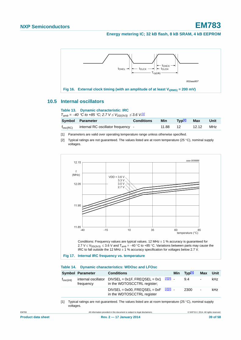
10.5 Internal oscillators
[1] Parameters are valid over operating temperature range unless otherwise specified.
[2] Typical ratings are not guaranteed. The values listed are at room temperature (25 C), nominal supply voltages.
[1] Typical ratings are not guaranteed. The values listed are at room temperature (25 C), nominal supply voltages.
Fig 16. External clock timing (with an amplitude of at least Vi(RMS) = 200 mV)
tCHCL tCLCX
tCHCX
Tcy(clk)
tCLCH
002aaa907
Table 13. Dynamic characteristic: IRCTamb = 40 C to +85 C; 2.7 V VDD(3V3) 3.6 V.[1]
Symbol Parameter Conditions Min Typ[2] Max Unit
fosc(RC) internal RC oscillator frequency - 11.88 12 12.12 MHz
Conditions: Frequency values are typical values. 12 MHz 1 % accuracy is guaranteed for 2.7 V VDD(3V3) 3.6 V and Tamb = 40 C to +85 C. Variations between parts may cause the IRC to fall outside the 12 MHz 1 % accuracy specification for voltages below 2.7 V.
Fig 17. Internal IRC frequency vs. temperature
Table 14. Dynamic characteristics: WDOsc and LFOsc
Symbol Parameter Conditions Min Typ[1] Max Unit
fosc(int) internal oscillator frequency
DIVSEL = 0x1F, FREQSEL = 0x1 in the WDTOSCCTRL register;
[2][3] - 9.4 - kHz
DIVSEL = 0x00, FREQSEL = 0xF in the WDTOSCCTRL register
[2][3] - 2300 - kHz
aaa-009888
11.95
12.05
12.15
f(MHz)
11.85
temperature (°C)-40 853510 60-15
VDD = 3.6 V3.3 V3.0 V2.7 V
EM783 All information provided in this document is subject to legal disclaimers. © NXP B.V. 2014. All rights reserved.
Product data sheet Rev. 2 — 17 January 2014 39 of 58
NXP Semiconductors EM783Energy metering IC; 32 kB flash, 8 kB SRAM, 4 kB EEPROM
[2] The typical frequency spread over processing and temperature (Tamb = 40 C to +85 C) is 40 %.
[3] See the EM783 user manual.
10.6 I/O pins
[1] Applies to standard port pins and RESET pin. Simulated results.
[2] SSO indicates maximum number of simultaneously switching digital output pins. The pins are optimized for half of the maximum SSO.
[3] Set SLEW bit in the IOCONFIG register to 1.
[4] Set SLEW bit in the IOCONFIG register to 0.
10.7 I2C-bus
Remark: All I2C modes (Standard-mode, Fast-mode, Fast-mode Plus) can be configured for the true open-drain pins P0_2 and P0_3. If the limited-performance I2C-bus pins are used (I2C-bus functions on standard I/O pins), only Standard-mode with internal pull-up enabled or Fast-mode with external pull-up resistor are supported.
Table 15. Dynamic characteristic: digital I/O pins[1]
Tamb = 40 C to +85 C; 3.0 V VDD(IO) 3.6 V; load capacitor = 30 pF.
Symbol Parameter Conditions Min Typ Max Unit
tr rise time pin configured as output
SSO = 1 [2][3] 2.5 - 5.0 ns
SSO = 6 [2][3] 2.5 - 4.5 ns
SSO = 16 [2][4] 3.0 - 5.0 ns
tf fall time pin configured as output
SSO = 1
[2][3]
2.0 - 4.5 ns
SSO = 6 [2][3] 2.0 - 4.5 ns
SSO = 16 [2][4] 2.5 - 5.0 ns
Table 16. Dynamic characteristic: I2C-bus pins[1]
Tamb = 40 C to +85 C.[2]
Symbol Parameter Conditions Min Max Unit
fSCL SCL clock frequency
Standard-mode 0 100 kHz
Fast-mode 0 400 kHz
Fast-mode Plus 0 1 MHz
tf fall time [4][5][6][7] of both SDA and SCL signals
Standard-mode
- 300 ns
Fast-mode 20 + 0.1 Cb 300 ns
Fast-mode Plus - 120 ns
tLOW LOW period of the SCL clock
Standard-mode 4.7 - s
Fast-mode 1.3 - s
Fast-mode Plus 0.5 - s
EM783 All information provided in this document is subject to legal disclaimers. © NXP B.V. 2014. All rights reserved.
Product data sheet Rev. 2 — 17 January 2014 40 of 58
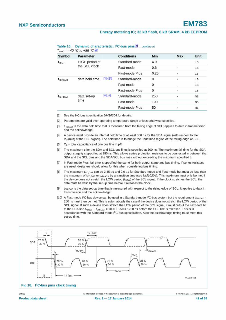
NXP Semiconductors EM783Energy metering IC; 32 kB flash, 8 kB SRAM, 4 kB EEPROM
[1] See the I2C-bus specification UM10204 for details.
[2] Parameters are valid over operating temperature range unless otherwise specified.
[3] tHD;DAT is the data hold time that is measured from the falling edge of SCL; applies to data in transmission and the acknowledge.
[4] A device must provide an internal hold time of at least 300 ns for the SDA signal (with respect to the VIH(min) of the SCL signal). The hold time is to bridge the undefined region of the falling edge of SCL.
[5] Cb = total capacitance of one bus line in pF.
[6] The maximum tf for the SDA and SCL bus lines is specified at 300 ns. The maximum fall time for the SDA output stage tf is specified at 250 ns. This allows series protection resistors to be connected in between the SDA and the SCL pins and the SDA/SCL bus lines without exceeding the maximum specified tf.
[7] In Fast-mode Plus, fall time is specified the same for both output stage and bus timing. If series resistors are used, designers should allow for this when considering bus timing.
[8] The maximum tHD;DAT can be 3.45 s and 0.9 s for Standard-mode and Fast-mode but must be less than the maximum of tVD;DAT or tVD;ACK by a transition time (see UM10204). This maximum must only be met if the device does not stretch the LOW period (tLOW) of the SCL signal. If the clock stretches the SCL, the data must be valid by the set-up time before it releases the clock.
[9] tSU;DAT is the data set-up time that is measured with respect to the rising edge of SCL. It applies to data in transmission and the acknowledge.
[10] A Fast-mode I2C-bus device can be used in a Standard-mode I2C-bus system but the requirement tSU;DAT = 250 ns must then be met. This is automatically the case if the device does not stretch the LOW period of the SCL signal. If such a device does stretch the LOW period of the SCL signal, it must output the next data bit to the SDA line tr(max) + tSU;DAT = 1000 + 250 = 1250 ns before the SCL line is released. This is in accordance with the Standard-mode I2C-bus specification. Also the acknowledge timing must meet this set-up time.
tHIGH HIGH period of the SCL clock
Standard-mode 4.0 - s
Fast-mode 0.6 - s
Fast-mode Plus 0.26 - s
tHD;DAT data hold time [3][4][8] Standard-mode 0 - s
Fast-mode 0 - s
Fast-mode Plus 0 - s
tSU;DAT data set-up time
[9][10] Standard-mode 250 - ns
Fast-mode 100 - ns
Fast-mode Plus 50 - ns
Table 16. Dynamic characteristic: I2C-bus pins[1] …continuedTamb = 40 C to +85 C.[2]
Symbol Parameter Conditions Min Max Unit
Fig 18. I2C-bus pins clock timing
002aaf425
tf
70 %30 %SDA
tf
70 %30 %
S
70 %30 %
70 %30 %
tHD;DAT
SCL
1 / fSCL
70 %30 %
70 %30 %
tVD;DATtHIGH
tLOW
tSU;DAT
EM783 All information provided in this document is subject to legal disclaimers. © NXP B.V. 2014. All rights reserved.
Product data sheet Rev. 2 — 17 January 2014 41 of 58
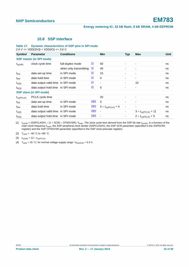
NXP Semiconductors EM783Energy metering IC; 32 kB flash, 8 kB SRAM, 4 kB EEPROM
10.8 SSP interface
[1] tcy(clk) = (SSPCLKDIV (1 + SCR) CPSDVSR) / fmain. The clock cycle time derived from the SSP bit rate tcy(clk), is a function of the main clock frequency fmain, the SSP peripheral clock divider (SSPCLKDIV), the SSP SCR parameter (specified in the SSP0CR0 register) and the SSP CPSDVSR parameter (specified in the SSP clock prescale register).
[2] Tamb = 40 C to +85 C.
[3] tcy(clk) = 12 tcy(PCLK).
[4] Tamb = 25 C; for normal voltage supply range: VDD(3V3) = 3.3 V.
Table 17. Dynamic characteristics of SSP pins in SPI mode 2.6 V <= VDD(3V3) = VDD(IO) <= 3.6 V.
Symbol Parameter Conditions Min Typ Max Unit
SSP master (in SPI mode)
tcy(clk) clock cycle time full-duplex mode [1] 50 - - ns
when only transmitting [1] 40 - - ns
tDS data set-up time in SPI mode [2] 15 - - ns
tDH data hold time in SPI mode [2] 0 - - ns
tv(Q) data output valid time in SPI mode [2] - - 10 ns
th(Q) data output hold time in SPI mode [2] 0 - - ns
SSP slave (in SPI mode)
tcy(PCLK) PCLK cycle time 20 - - ns
tDS data set-up time in SPI mode [3][4] 0 - - ns
tDH data hold time in SPI mode [3][4] 3 tcy(PCLK) + 4 - - ns
tv(Q) data output valid time in SPI mode [3][4] - - 3 tcy(PCLK) + 11 ns
th(Q) data output hold time in SPI mode [3][4] - - 2 tcy(PCLK) + 5 ns
EM783 All information provided in this document is subject to legal disclaimers. © NXP B.V. 2014. All rights reserved.
Product data sheet Rev. 2 — 17 January 2014 42 of 58
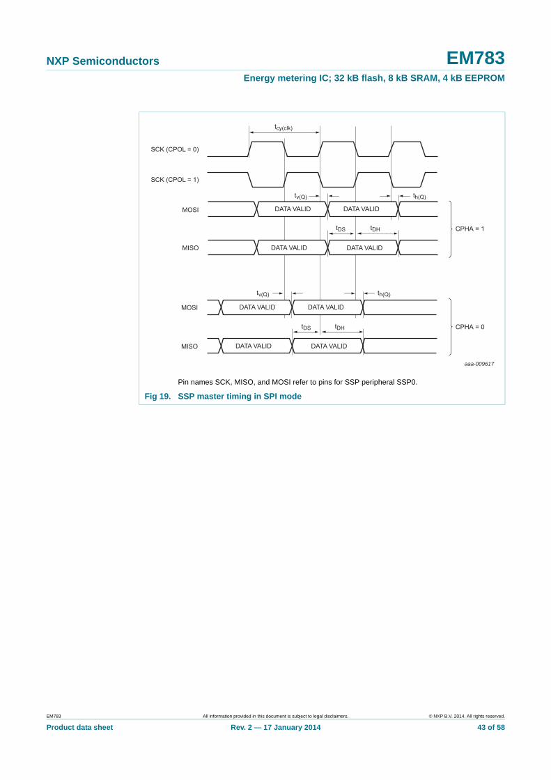
NXP Semiconductors EM783Energy metering IC; 32 kB flash, 8 kB SRAM, 4 kB EEPROM
Pin names SCK, MISO, and MOSI refer to pins for SSP peripheral SSP0.
Fig 19. SSP master timing in SPI mode
SCK (CPOL = 0)
MOSI
MISO
tcy(clk)
tDS tDH
tv(Q)
DATA VALID DATA VALID
th(Q)
SCK (CPOL = 1)
DATA VALID DATA VALID
MOSI
MISO
tDS tDH
DATA VALID DATA VALID
th(Q)
DATA VALID DATA VALID
tv(Q)
CPHA = 1
CPHA = 0
aaa-009617
EM783 All information provided in this document is subject to legal disclaimers. © NXP B.V. 2014. All rights reserved.
Product data sheet Rev. 2 — 17 January 2014 43 of 58
NXP Semiconductors EM783Energy metering IC; 32 kB flash, 8 kB SRAM, 4 kB EEPROM
11. Characteristics of analog peripherals
[1] Interrupt levels are selected by writing the level value to the BOD control register BODCTRL, see EM783 User manual.
Pin names SCK, MISO, and MOSI refer to pins for SSP peripheral SSP0.
Fig 20. SSP slave timing in SPI mode
SCK (CPOL = 0)
MOSI
MISO
tcy(clk)
tDS tDH
tv(Q)
DATA VALID DATA VALID
th(Q)
SCK (CPOL = 1)
DATA VALID DATA VALID
MOSI
MISO
tDS tDH
tv(Q)
DATA VALID DATA VALID
th(Q)
DATA VALID DATA VALID
CPHA = 1
CPHA = 0
aaa-009618
Table 18. BOD static characteristics[1]
Tamb = 25 C.
Symbol Parameter Conditions Min Typ Max Unit
Vth threshold voltage interrupt level 2
assertion - 2.52 - V
de-assertion - 2.66 - V
interrupt level 3
assertion - 2.80 - V
de-assertion - 2.90 - V
EM783 All information provided in this document is subject to legal disclaimers. © NXP B.V. 2014. All rights reserved.
Product data sheet Rev. 2 — 17 January 2014 44 of 58
NXP Semiconductors EM783Energy metering IC; 32 kB flash, 8 kB SRAM, 4 kB EEPROM
[1] Measured on typical samples.
[1] Characterized through simulation.
[2] Characterized on a typical silicon sample.
[3] Measured over process variations.
Table 19. DAC static and dynamic characteristicsVDD(3V3) = 2.7 V to 3.6 V; Tamb = 40 C to +85 C unless otherwise specified
Symbol Parameter Conditions Min Typ Max Unit
ED differential linearity error
- - 1 LSB
EL(adj) integral non-linearity
- - 2 LSB
EO offset error - - 25 mV
EG gain error - - 25 mV
CL load capacitance - - 200 pF
RL load resistance 1 - - k
RO output resistance [1] - < 40
fc(DAC) DAC conversion frequency
- 0.4 1 MHz
ts settling time - - 1 s
VO output voltage Output voltage range with less than 1 LSB deviation; with minimum RL connected to ground or power supply
0.3 - VDD(3V3) 0.3
V
with minimum RL connected to ground or power supply
0.175 - VDD(3V3) 0.175
V
Table 20. DAC sampling frequency range and power consumption
Bias bit Maximum current DAC sampling frequency range
0 700 A 0 MHz to 1 MHz
1 350 A 0 MHz to 400 kHz
Table 21. Internal voltage reference static and dynamic characteristics
Symbol Parameter Conditions Min Typ Max Unit
VO output voltage Tamb = 40 C to +85 C [1] 0.855 0.900 0.945 V
Tamb = 70 C to +85 C [2] - 0.906 - V
Tamb = 50 C [2] - 0.905 - V
Tamb = 25 C [3] 0.893 0.903 0.913 V
Tamb = 0 C [2] - 0.902 - V
Tamb = 20 C [2] - 0.899 - V
Tamb = 40 C [2] - 0.896 - V
ts(pu) power-up settling time
up to 90 % of VO[3] - 144 195 s
EM783 All information provided in this document is subject to legal disclaimers. © NXP B.V. 2014. All rights reserved.
Product data sheet Rev. 2 — 17 January 2014 45 of 58
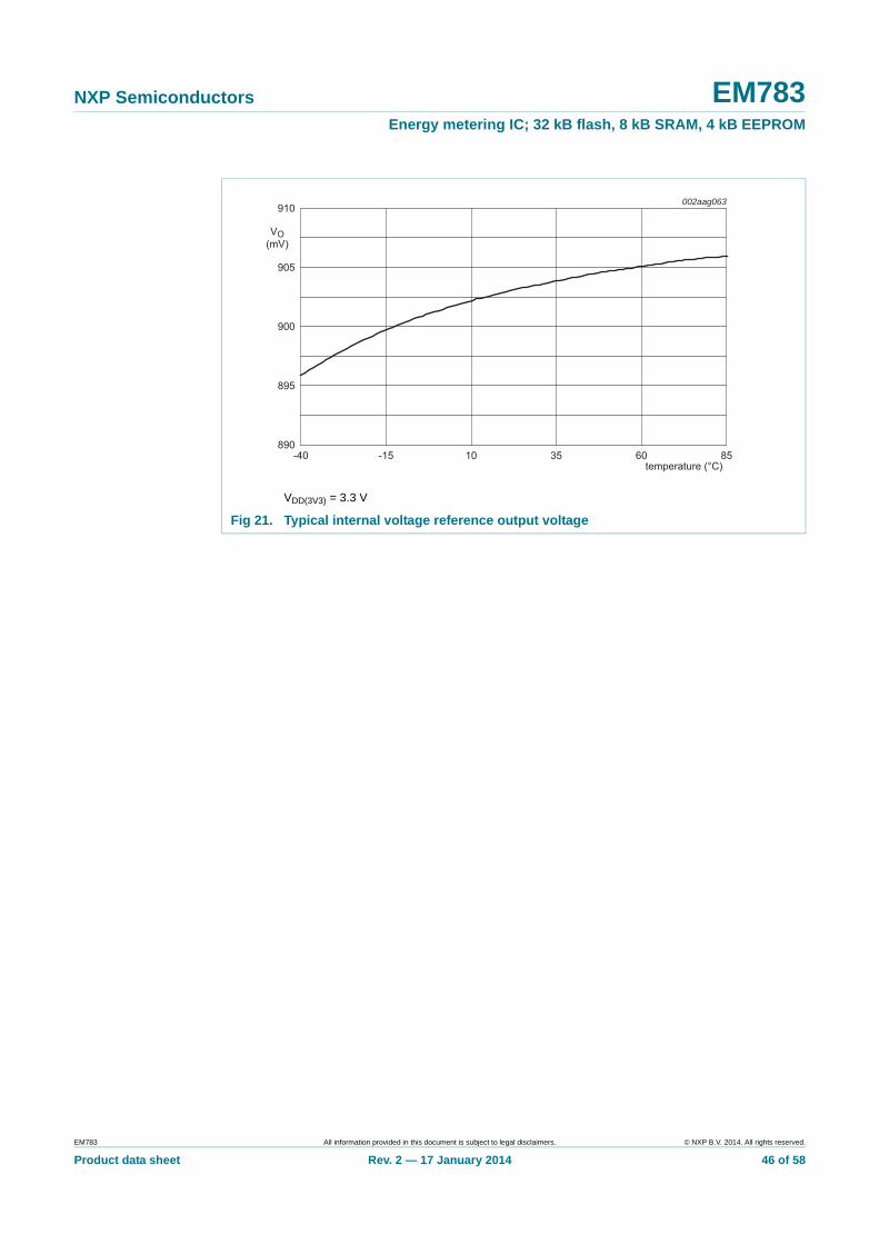
NXP Semiconductors EM783Energy metering IC; 32 kB flash, 8 kB SRAM, 4 kB EEPROM
VDD(3V3) = 3.3 V
Fig 21. Typical internal voltage reference output voltage
002aag063
temperature (°C)-40 853510 60-15
895
905
900
910
VO(mV)
890
EM783 All information provided in this document is subject to legal disclaimers. © NXP B.V. 2014. All rights reserved.
Product data sheet Rev. 2 — 17 January 2014 46 of 58
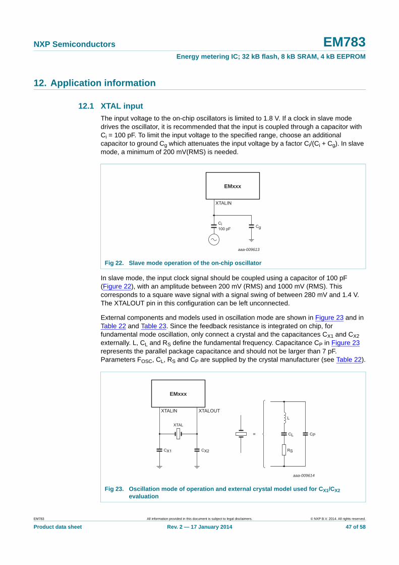
NXP Semiconductors EM783Energy metering IC; 32 kB flash, 8 kB SRAM, 4 kB EEPROM
12. Application information
12.1 XTAL input
The input voltage to the on-chip oscillators is limited to 1.8 V. If a clock in slave mode drives the oscillator, it is recommended that the input is coupled through a capacitor with Ci = 100 pF. To limit the input voltage to the specified range, choose an additional capacitor to ground Cg which attenuates the input voltage by a factor Ci/(Ci + Cg). In slave mode, a minimum of 200 mV(RMS) is needed.
In slave mode, the input clock signal should be coupled using a capacitor of 100 pF (Figure 22), with an amplitude between 200 mV (RMS) and 1000 mV (RMS). This corresponds to a square wave signal with a signal swing of between 280 mV and 1.4 V. The XTALOUT pin in this configuration can be left unconnected.
External components and models used in oscillation mode are shown in Figure 23 and in Table 22 and Table 23. Since the feedback resistance is integrated on chip, for fundamental mode oscillation, only connect a crystal and the capacitances CX1 and CX2 externally. L, CL and RS define the fundamental frequency. Capacitance CP in Figure 23 represents the parallel package capacitance and should not be larger than 7 pF. Parameters FOSC, CL, RS and CP are supplied by the crystal manufacturer (see Table 22).
Fig 22. Slave mode operation of the on-chip oscillator
Fig 23. Oscillation mode of operation and external crystal model used for CX1/CX2 evaluation
aaa-009613
EMxxx
CgCi100 pF
XTALIN
aaa-009614
EMxxx
XTALOUT
XTAL
=
CX2 RS
L
CL CP
CX1
XTALIN
EM783 All information provided in this document is subject to legal disclaimers. © NXP B.V. 2014. All rights reserved.
Product data sheet Rev. 2 — 17 January 2014 47 of 58
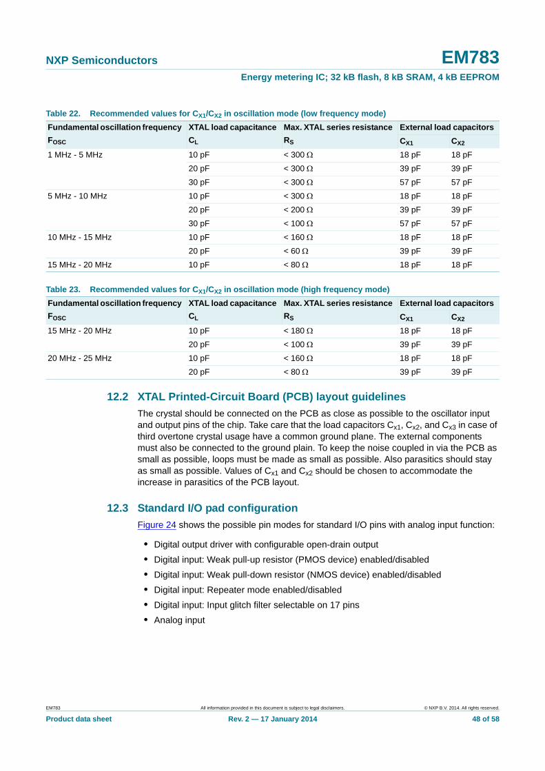
NXP Semiconductors EM783Energy metering IC; 32 kB flash, 8 kB SRAM, 4 kB EEPROM
12.2 XTAL Printed-Circuit Board (PCB) layout guidelines
The crystal should be connected on the PCB as close as possible to the oscillator input and output pins of the chip. Take care that the load capacitors Cx1, Cx2, and Cx3 in case of third overtone crystal usage have a common ground plane. The external components must also be connected to the ground plain. To keep the noise coupled in via the PCB as small as possible, loops must be made as small as possible. Also parasitics should stay as small as possible. Values of Cx1 and Cx2 should be chosen to accommodate the increase in parasitics of the PCB layout.
12.3 Standard I/O pad configuration
Figure 24 shows the possible pin modes for standard I/O pins with analog input function:
• Digital output driver with configurable open-drain output
• Digital input: Weak pull-up resistor (PMOS device) enabled/disabled
• Digital input: Weak pull-down resistor (NMOS device) enabled/disabled
• Digital input: Repeater mode enabled/disabled
• Digital input: Input glitch filter selectable on 17 pins
• Analog input
Table 22. Recommended values for CX1/CX2 in oscillation mode (low frequency mode)
Fundamental oscillation frequency
FOSC
XTAL load capacitance
CL
Max. XTAL series resistance
RS
External load capacitors
CX1 CX2
1 MHz - 5 MHz 10 pF < 300 18 pF 18 pF
20 pF < 300 39 pF 39 pF
30 pF < 300 57 pF 57 pF
5 MHz - 10 MHz 10 pF < 300 18 pF 18 pF
20 pF < 200 39 pF 39 pF
30 pF < 100 57 pF 57 pF
10 MHz - 15 MHz 10 pF < 160 18 pF 18 pF
20 pF < 60 39 pF 39 pF
15 MHz - 20 MHz 10 pF < 80 18 pF 18 pF
Table 23. Recommended values for CX1/CX2 in oscillation mode (high frequency mode)
Fundamental oscillation frequency
FOSC
XTAL load capacitance
CL
Max. XTAL series resistance
RS
External load capacitors
CX1 CX2
15 MHz - 20 MHz 10 pF < 180 18 pF 18 pF
20 pF < 100 39 pF 39 pF
20 MHz - 25 MHz 10 pF < 160 18 pF 18 pF
20 pF < 80 39 pF 39 pF
EM783 All information provided in this document is subject to legal disclaimers. © NXP B.V. 2014. All rights reserved.
Product data sheet Rev. 2 — 17 January 2014 48 of 58
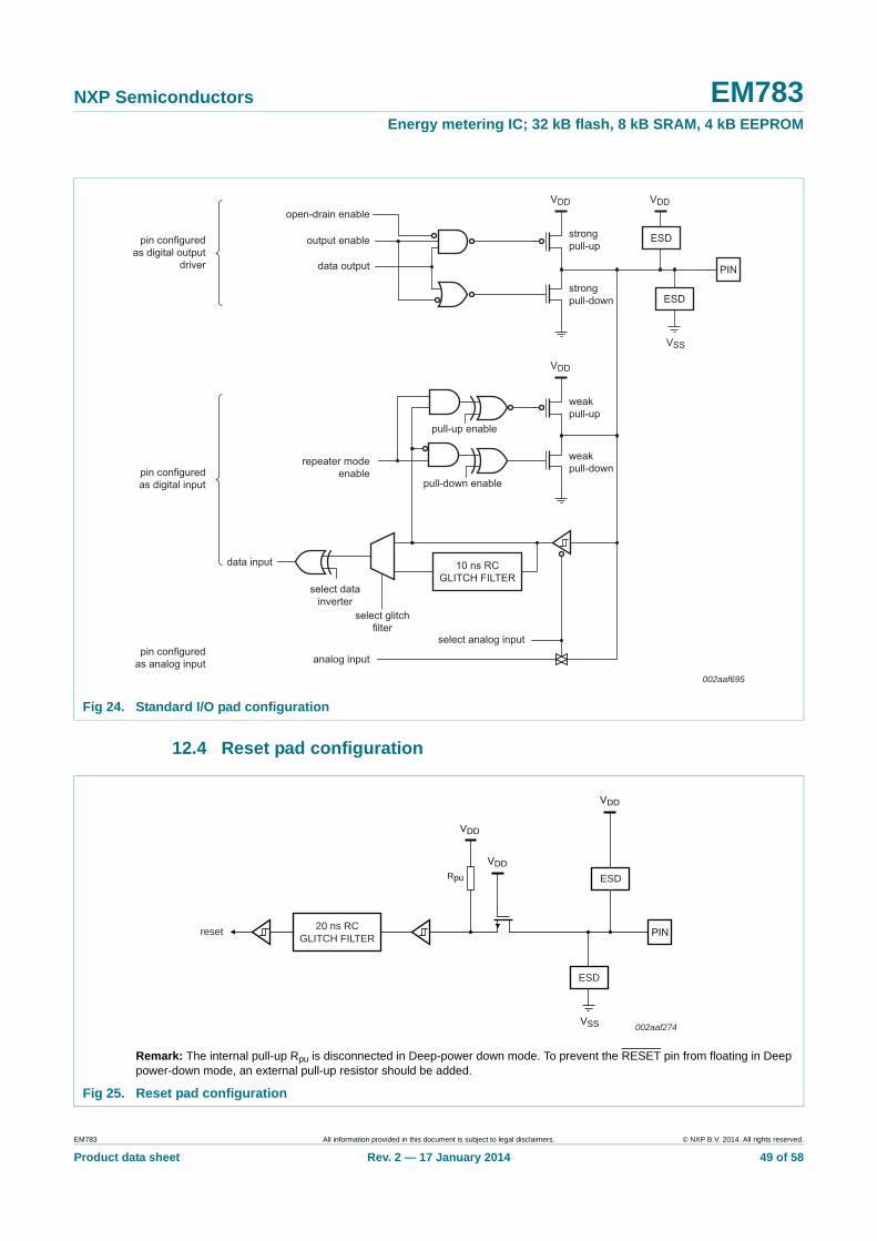
NXP Semiconductors EM783Energy metering IC; 32 kB flash, 8 kB SRAM, 4 kB EEPROM
12.4 Reset pad configuration
Fig 24. Standard I/O pad configuration
PIN
VDD VDD
ESD
VSS
ESD
strongpull-up
strongpull-down
VDD
weakpull-up
weakpull-down
open-drain enable
output enable
repeater modeenable
pull-up enable
pull-down enable
select datainverter
data output
data input
select glitchfilter
analog input
select analog input
002aaf695
pin configuredas digital output
driver
pin configuredas digital input
pin configuredas analog input
10 ns RCGLITCH FILTER
Remark: The internal pull-up Rpu is disconnected in Deep-power down mode. To prevent the RESET pin from floating in Deep power-down mode, an external pull-up resistor should be added.
Fig 25. Reset pad configuration
VSS
reset
002aaf274
VDD
VDD
VDD
Rpu ESD
ESD
20 ns RCGLITCH FILTER
PIN
EM783 All information provided in this document is subject to legal disclaimers. © NXP B.V. 2014. All rights reserved.
Product data sheet Rev. 2 — 17 January 2014 49 of 58
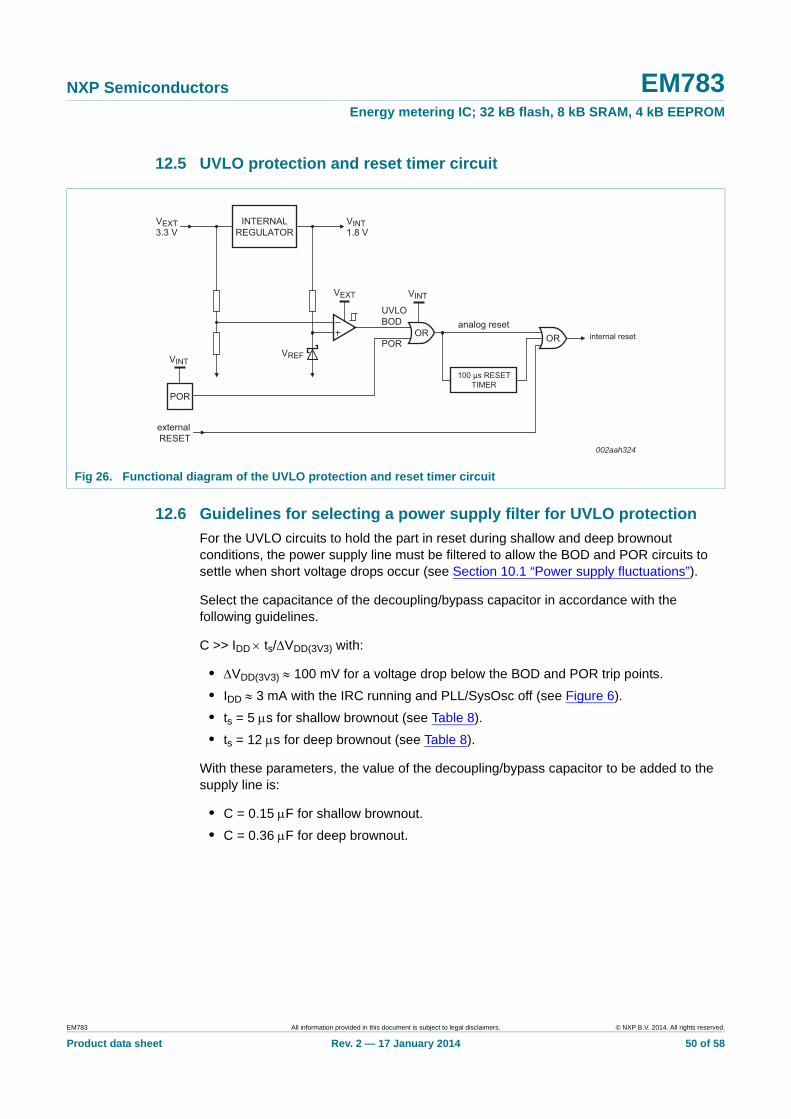
NXP Semiconductors EM783Energy metering IC; 32 kB flash, 8 kB SRAM, 4 kB EEPROM
12.5 UVLO protection and reset timer circuit
12.6 Guidelines for selecting a power supply filter for UVLO protection
For the UVLO circuits to hold the part in reset during shallow and deep brownout conditions, the power supply line must be filtered to allow the BOD and POR circuits to settle when short voltage drops occur (see Section 10.1 “Power supply fluctuations”).
Select the capacitance of the decoupling/bypass capacitor in accordance with the following guidelines.
C >> IDD ts/VDD(3V3) with:
• VDD(3V3) 100 mV for a voltage drop below the BOD and POR trip points.
• IDD 3 mA with the IRC running and PLL/SysOsc off (see Figure 6).
• ts = 5 s for shallow brownout (see Table 8).
• ts = 12 s for deep brownout (see Table 8).
With these parameters, the value of the decoupling/bypass capacitor to be added to the supply line is:
• C = 0.15 F for shallow brownout.
• C = 0.36 F for deep brownout.
Fig 26. Functional diagram of the UVLO protection and reset timer circuit
002aah324
INTERNALREGULATOR
VINT1.8 V
VEXT
VINT
VINT
analog reset
VREF
POR
VEXT3.3 V
UVLOBOD
POROR OR
externalRESET
internal reset
100 μs RESETTIMER
EM783 All information provided in this document is subject to legal disclaimers. © NXP B.V. 2014. All rights reserved.
Product data sheet Rev. 2 — 17 January 2014 50 of 58
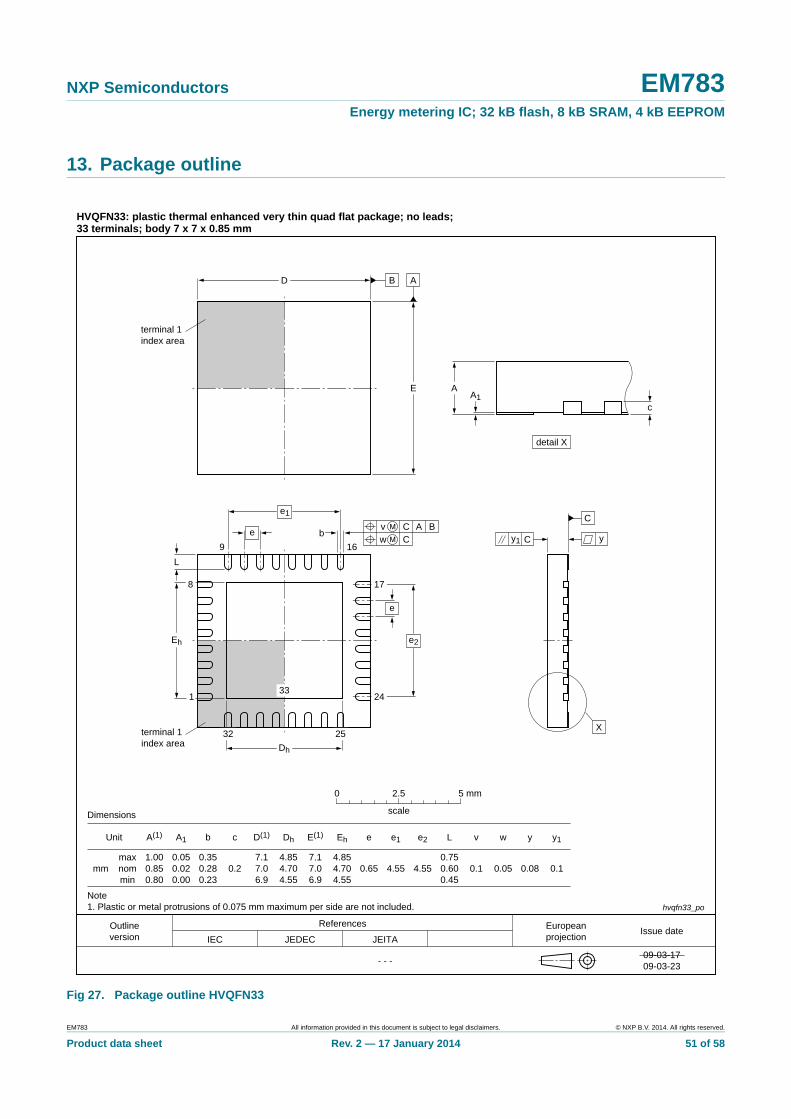
NXP Semiconductors EM783Energy metering IC; 32 kB flash, 8 kB SRAM, 4 kB EEPROM
13. Package outline
Fig 27. Package outline HVQFN33
ReferencesOutlineversion
Europeanprojection
Issue dateIEC JEDEC JEITA
- - -
hvqfn33_po
09-03-1709-03-23
Unit
mmmaxnommin
1.000.850.80
0.050.020.00
0.27.17.06.9
4.854.704.55
7.17.06.9
0.65 4.550.750.600.45
0.1
A(1)
Dimensions
Note1. Plastic or metal protrusions of 0.075 mm maximum per side are not included.
HVQFN33: plastic thermal enhanced very thin quad flat package; no leads;33 terminals; body 7 x 7 x 0.85 mm
A1 b
0.350.280.23
c D(1) Dh E(1) Eh
4.854.704.55
e e1 e2
4.55
L v
0.1
w
0.05
y
0.08
y1
0 2.5 5 mm
scale
terminal 1index area
B AD
E
C
yCy1
X
detail X
A1A
c
b
e2
e1
e
e
AC BvCw
terminal 1index area Dh
Eh
L
9 16
32
33
25
17
24
8
1
EM783 All information provided in this document is subject to legal disclaimers. © NXP B.V. 2014. All rights reserved.
Product data sheet Rev. 2 — 17 January 2014 51 of 58
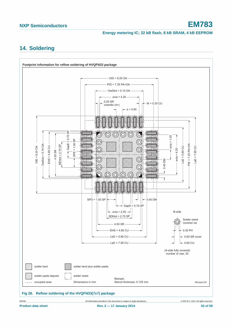
NXP Semiconductors EM783Energy metering IC; 32 kB flash, 8 kB SRAM, 4 kB EEPROM
14. Soldering
Fig 28. Reflow soldering of the HVQFN33(7x7) package
Footprint information for reflow soldering of HVQFN33 package
001aao134occupied area
solder land
solder resist
solder land plus solder paste
solder paste deposit
Dimensions in mmRemark:Stencil thickness: 0.125 mm
e = 0.65
evia = 4.25
OwDtot = 5.10 OA
PID = 7.25 PA+OA
OID = 8.20 OA
0.20 SRchamfer (4×)
0.45
DM
evia
= 1
.05
W = 0.30 CU
evia
= 4
.25
evia = 2.40
LbE
= 5
.80
CU
LbD = 5.80 CU
PIE
= 7
.25
PA+O
A
LaE
= 7
.95
CU
LaD = 7.95 CU
OIE
= 8
.20
OA
Ow
Eto
t = 5
.10
OA
EH
S =
4.8
5 C
U
DHS = 4.85 CU
4.55
SR
4.55 SR
B-side
(A-side fully covered)number of vias: 20
Solder resistcovered via
0.30 PH
0.60 SR cover
0.60 CU
SE
htot
= 2
.70
SP
SDhtot = 2.70 SP
Gap
E =
0.7
0 S
P
SP
E =
1.0
0 S
P
0.45 DMSPD = 1.00 SP
GapD = 0.70 SP
EM783 All information provided in this document is subject to legal disclaimers. © NXP B.V. 2014. All rights reserved.
Product data sheet Rev. 2 — 17 January 2014 52 of 58
NXP Semiconductors EM783Energy metering IC; 32 kB flash, 8 kB SRAM, 4 kB EEPROM
15. Abbreviations
16. Revision history
Table 24. Abbreviations
Acronym Description
AHB Advanced High-performance Bus
AMBA Advanced Microcontroller Bus Architecture
APB Advanced Peripheral Bus
BOD BrownOut Detection
GPIO General Purpose Input/Output
I2C Inter-Integrated Circuit
JEDEC Joint Electron Devices Engineering Council
NVM Non-Volatile Memory
PLL Phase-Locked Loop
SPI Serial Peripheral Interface
SSI Serial Synchronous Interface
TTL Transistor-Transistor Logic
USART Universal Synchronous/Asynchronous Receiver/Transmitter
UVLO Under-Voltage Lockout
Table 25. Revision history
Document ID Release date Data sheet status Change notice Supersedes
EM783 v.2 20140117 Product data sheet - EM783 v.1
EM783 v.1 20131108 Objective data sheet - -
EM783 All information provided in this document is subject to legal disclaimers. © NXP B.V. 2014. All rights reserved.
Product data sheet Rev. 2 — 17 January 2014 53 of 58
NXP Semiconductors EM783Energy metering IC; 32 kB flash, 8 kB SRAM, 4 kB EEPROM
17. Legal information
17.1 Data sheet status
[1] Please consult the most recently issued document before initiating or completing a design.
[2] The term ‘short data sheet’ is explained in section “Definitions”.
[3] The product status of device(s) described in this document may have changed since this document was published and may differ in case of multiple devices. The latest product status information is available on the Internet at URL http://www.nxp.com.
17.2 Definitions
Draft — The document is a draft version only. The content is still under internal review and subject to formal approval, which may result in modifications or additions. NXP Semiconductors does not give any representations or warranties as to the accuracy or completeness of information included herein and shall have no liability for the consequences of use of such information.
Short data sheet — A short data sheet is an extract from a full data sheet with the same product type number(s) and title. A short data sheet is intended for quick reference only and should not be relied upon to contain detailed and full information. For detailed and full information see the relevant full data sheet, which is available on request via the local NXP Semiconductors sales office. In case of any inconsistency or conflict with the short data sheet, the full data sheet shall prevail.
Product specification — The information and data provided in a Product data sheet shall define the specification of the product as agreed between NXP Semiconductors and its customer, unless NXP Semiconductors and customer have explicitly agreed otherwise in writing. In no event however, shall an agreement be valid in which the NXP Semiconductors product is deemed to offer functions and qualities beyond those described in the Product data sheet.
17.3 Disclaimers
Limited warranty and liability — Information in this document is believed to be accurate and reliable. However, NXP Semiconductors does not give any representations or warranties, expressed or implied, as to the accuracy or completeness of such information and shall have no liability for the consequences of use of such information. NXP Semiconductors takes no responsibility for the content in this document if provided by an information source outside of NXP Semiconductors.
In no event shall NXP Semiconductors be liable for any indirect, incidental, punitive, special or consequential damages (including - without limitation - lost profits, lost savings, business interruption, costs related to the removal or replacement of any products or rework charges) whether or not such damages are based on tort (including negligence), warranty, breach of contract or any other legal theory.
Notwithstanding any damages that customer might incur for any reason whatsoever, NXP Semiconductors’ aggregate and cumulative liability towards customer for the products described herein shall be limited in accordance with the Terms and conditions of commercial sale of NXP Semiconductors.
Right to make changes — NXP Semiconductors reserves the right to make changes to information published in this document, including without limitation specifications and product descriptions, at any time and without notice. This document supersedes and replaces all information supplied prior to the publication hereof.
Suitability for use — NXP Semiconductors products are not designed, authorized or warranted to be suitable for use in life support, life-critical or safety-critical systems or equipment, nor in applications where failure or malfunction of an NXP Semiconductors product can reasonably be expected to result in personal injury, death or severe property or environmental damage. NXP Semiconductors and its suppliers accept no liability for inclusion and/or use of NXP Semiconductors products in such equipment or applications and therefore such inclusion and/or use is at the customer’s own risk.
Applications — Applications that are described herein for any of these products are for illustrative purposes only. NXP Semiconductors makes no representation or warranty that such applications will be suitable for the specified use without further testing or modification.
Customers are responsible for the design and operation of their applications and products using NXP Semiconductors products, and NXP Semiconductors accepts no liability for any assistance with applications or customer product design. It is customer’s sole responsibility to determine whether the NXP Semiconductors product is suitable and fit for the customer’s applications and products planned, as well as for the planned application and use of customer’s third party customer(s). Customers should provide appropriate design and operating safeguards to minimize the risks associated with their applications and products.
NXP Semiconductors does not accept any liability related to any default, damage, costs or problem which is based on any weakness or default in the customer’s applications or products, or the application or use by customer’s third party customer(s). Customer is responsible for doing all necessary testing for the customer’s applications and products using NXP Semiconductors products in order to avoid a default of the applications and the products or of the application or use by customer’s third party customer(s). NXP does not accept any liability in this respect.
Limiting values — Stress above one or more limiting values (as defined in the Absolute Maximum Ratings System of IEC 60134) will cause permanent damage to the device. Limiting values are stress ratings only and (proper) operation of the device at these or any other conditions above those given in the Recommended operating conditions section (if present) or the Characteristics sections of this document is not warranted. Constant or repeated exposure to limiting values will permanently and irreversibly affect the quality and reliability of the device.
Terms and conditions of commercial sale — NXP Semiconductors products are sold subject to the general terms and conditions of commercial sale, as published at http://www.nxp.com/profile/terms, unless otherwise agreed in a valid written individual agreement. In case an individual agreement is concluded only the terms and conditions of the respective agreement shall apply. NXP Semiconductors hereby expressly objects to applying the customer’s general terms and conditions with regard to the purchase of NXP Semiconductors products by customer.
No offer to sell or license — Nothing in this document may be interpreted or construed as an offer to sell products that is open for acceptance or the grant, conveyance or implication of any license under any copyrights, patents or other industrial or intellectual property rights.
Document status[1][2] Product status[3] Definition
Objective [short] data sheet Development This document contains data from the objective specification for product development.
Preliminary [short] data sheet Qualification This document contains data from the preliminary specification.
Product [short] data sheet Production This document contains the product specification.
EM783 All information provided in this document is subject to legal disclaimers. © NXP B.V. 2014. All rights reserved.
Product data sheet Rev. 2 — 17 January 2014 54 of 58
NXP Semiconductors EM783Energy metering IC; 32 kB flash, 8 kB SRAM, 4 kB EEPROM
Export control — This document as well as the item(s) described herein may be subject to export control regulations. Export might require a prior authorization from competent authorities.
Quick reference data — The Quick reference data is an extract of the product data given in the Limiting values and Characteristics sections of this document, and as such is not complete, exhaustive or legally binding.
Non-automotive qualified products — Unless this data sheet expressly states that this specific NXP Semiconductors product is automotive qualified, the product is not suitable for automotive use. It is neither qualified nor tested in accordance with automotive testing or application requirements. NXP Semiconductors accepts no liability for inclusion and/or use of non-automotive qualified products in automotive equipment or applications.
In the event that customer uses the product for design-in and use in automotive applications to automotive specifications and standards, customer (a) shall use the product without NXP Semiconductors’ warranty of the product for such automotive applications, use and specifications, and (b)
whenever customer uses the product for automotive applications beyond NXP Semiconductors’ specifications such use shall be solely at customer’s own risk, and (c) customer fully indemnifies NXP Semiconductors for any liability, damages or failed product claims resulting from customer design and use of the product for automotive applications beyond NXP Semiconductors’ standard warranty and NXP Semiconductors’ product specifications.
Translations — A non-English (translated) version of a document is for reference only. The English version shall prevail in case of any discrepancy between the translated and English versions.
17.4 TrademarksNotice: All referenced brands, product names, service names and trademarks are the property of their respective owners.
I2C-bus — logo is a trademark of NXP B.V.
18. Contact information
For more information, please visit: http://www.nxp.com
For sales office addresses, please send an email to: [email protected]
EM783 All information provided in this document is subject to legal disclaimers. © NXP B.V. 2014. All rights reserved.
Product data sheet Rev. 2 — 17 January 2014 55 of 58
NXP Semiconductors EM783Energy metering IC; 32 kB flash, 8 kB SRAM, 4 kB EEPROM
19. Tables
Table 1. Ordering information . . . . . . . . . . . . . . . . . . . . .3Table 2. Ordering options . . . . . . . . . . . . . . . . . . . . . . . .3Table 3. Pin multiplexing . . . . . . . . . . . . . . . . . . . . . . . .5Table 4. EM783 pin description . . . . . . . . . . . . . . . . . . .8Table 5. Limiting values . . . . . . . . . . . . . . . . . . . . . . . . .25Table 6. Static characteristics . . . . . . . . . . . . . . . . . . . .26Table 7. Power consumption for individual analog
and digital blocks . . . . . . . . . . . . . . . . . . . . . . .31Table 8. POR and BOD circuit settling characteristics . .35Table 9. Power supply ramp characteristics . . . . . . . . .36Table 10. Flash characteristics . . . . . . . . . . . . . . . . . . . . .38Table 11. EEPROM characteristics . . . . . . . . . . . . . . . . .38Table 12. Dynamic characteristic: external clock
(XTALIN or CLKIN pin) . . . . . . . . . . . . . . . . . .38Table 13. Dynamic characteristic: IRC . . . . . . . . . . . . . . .39Table 14. Dynamic characteristics: WDOsc and LFOsc. .39
Table 15. Dynamic characteristic: digital I/O pins[1] . . . . . 40Table 16. Dynamic characteristic: I2C-bus pins[1] . . . . . . 40Table 17. Dynamic characteristics of SSP pins in
SPI mode . . . . . . . . . . . . . . . . . . . . . . . . . . . . 42Table 18. BOD static characteristics[1] . . . . . . . . . . . . . . . 44Table 19. DAC static and dynamic characteristics . . . . . 45Table 20. DAC sampling frequency range and power
consumption. . . . . . . . . . . . . . . . . . . . . . . . . . . 45Table 21. Internal voltage reference static and dynamic
characteristics . . . . . . . . . . . . . . . . . . . . . . . . . 45Table 22. Recommended values for CX1/CX2 in oscillation
mode (low frequency mode) . . . . . . . . . . . . . . 48Table 23. Recommended values for CX1/CX2 in oscillation
mode (high frequency mode) . . . . . . . . . . . . . . 48Table 24. Abbreviations . . . . . . . . . . . . . . . . . . . . . . . . . 53Table 25. Revision history . . . . . . . . . . . . . . . . . . . . . . . . 53
20. Figures
Fig 1. EM783 block diagram . . . . . . . . . . . . . . . . . . . . . .4Fig 2. Pin configuration HVQFN33 package . . . . . . . . . .5Fig 3. EM783 memory map . . . . . . . . . . . . . . . . . . . . . .14Fig 4. EM783 clock generation block diagram. . . . . . . .21Fig 5. Active mode: Typical supply current IDD versus
temperature for different system clock frequencies (all peripherals disabled) . . . . . . . . . . . . . . . . . . .29
Fig 6. Active mode: Typical supply current IDD versus temperature for different system clock frequencies (all peripherals enabled) . . . . . . . . . . . . . . . . . . .30
Fig 7. Sleep mode: Typical supply current IDDversus temperature for different system clock frequencies (all peripherals disabled) . . . . . . . . . . . . . . . . . . .30
Fig 8. High-current source output driver: Typical HIGH-level output voltage VOH versus HIGH-level output current IOH . . . . . . . . . . . . . . .31
Fig 9. High-current sink pins: Typical LOW-level output current IOL versus LOW-level output voltage VOL. . . . . . . . . . . . . . . . . . . . . . . . . . . . . . . . . . . .32
Fig 10. Typical LOW-level output current IOL versus LOW-level output voltage VOL . . . . . . . . . . . . . . .32
Fig 11. Typical HIGH-level output voltage VOH versus HIGH-level output source current IOH . . . . . . . . .33
Fig 12. Typical pull-up current Ipu versus input voltage VI . . . . . . . . . . . . . . . . . . . . . . . . . . . . . . . . . . . . .33
Fig 13. Typical pull-down current Ipd versus input voltage VI . . . . . . . . . . . . . . . . . . . . . . . . . . . . . . .34
Fig 14. UVLO timing . . . . . . . . . . . . . . . . . . . . . . . . . . . .35Fig 15. Power supply voltage profile . . . . . . . . . . . . . . . .37Fig 16. External clock timing (with an amplitude
of at least Vi(RMS) = 200 mV) . . . . . . . . . . . . . . . .39Fig 17. Internal IRC frequency vs. temperature. . . . . . . .39Fig 18. I2C-bus pins clock timing . . . . . . . . . . . . . . . . . . .41Fig 19. SSP master timing in SPI mode. . . . . . . . . . . . . .43Fig 20. SSP slave timing in SPI mode . . . . . . . . . . . . . . .44Fig 21. Typical internal voltage reference output voltage.46
Fig 22. Slave mode operation of the on-chip oscillator . . 47Fig 23. Oscillation mode of operation and external crystal
model used for CX1/CX2 evaluation . . . . . . . . . . . 47Fig 24. Standard I/O pad configuration . . . . . . . . . . . . . . 49Fig 25. Reset pad configuration . . . . . . . . . . . . . . . . . . . 49Fig 26. Functional diagram of the UVLO protection and
reset timer circuit. . . . . . . . . . . . . . . . . . . . . . . . . 50Fig 27. Package outline HVQFN33 . . . . . . . . . . . . . . . . . 51Fig 28. Reflow soldering of the HVQFN33(7x7) package 52
EM783 All information provided in this document is subject to legal disclaimers. © NXP B.V. 2014. All rights reserved.
Product data sheet Rev. 2 — 17 January 2014 56 of 58
NXP Semiconductors EM783Energy metering IC; 32 kB flash, 8 kB SRAM, 4 kB EEPROM
21. Contents
1 General description . . . . . . . . . . . . . . . . . . . . . . 1
2 Features and benefits . . . . . . . . . . . . . . . . . . . . 1
3 Applications . . . . . . . . . . . . . . . . . . . . . . . . . . . . 3
4 Ordering information. . . . . . . . . . . . . . . . . . . . . 34.1 Ordering options . . . . . . . . . . . . . . . . . . . . . . . . 3
5 Block diagram . . . . . . . . . . . . . . . . . . . . . . . . . . 4
6 Pinning information. . . . . . . . . . . . . . . . . . . . . . 56.1 Pinning . . . . . . . . . . . . . . . . . . . . . . . . . . . . . . . 56.2 Pin description . . . . . . . . . . . . . . . . . . . . . . . . . 5
7 Functional description . . . . . . . . . . . . . . . . . . 137.1 ARM Cortex-M0 processor . . . . . . . . . . . . . . . 137.2 On-chip flash program memory . . . . . . . . . . . 137.3 On-chip EEPROM data memory. . . . . . . . . . . 137.4 On-chip SRAM . . . . . . . . . . . . . . . . . . . . . . . . 137.5 Memory map. . . . . . . . . . . . . . . . . . . . . . . . . . 137.6 Nested Vectored Interrupt Controller (NVIC) . 147.6.1 Features . . . . . . . . . . . . . . . . . . . . . . . . . . . . . 147.6.2 Interrupt sources. . . . . . . . . . . . . . . . . . . . . . . 157.7 IOCONFIG block . . . . . . . . . . . . . . . . . . . . . . 157.8 Fast general-purpose parallel I/O . . . . . . . . . . 157.8.1 Features . . . . . . . . . . . . . . . . . . . . . . . . . . . . . 157.9 USART . . . . . . . . . . . . . . . . . . . . . . . . . . . . . . 167.9.1 Features . . . . . . . . . . . . . . . . . . . . . . . . . . . . . 167.10 SSP serial I/O controller . . . . . . . . . . . . . . . . . 167.10.1 Features . . . . . . . . . . . . . . . . . . . . . . . . . . . . . 167.11 I2C-bus serial I/O controller . . . . . . . . . . . . . . 177.11.1 Features . . . . . . . . . . . . . . . . . . . . . . . . . . . . . 177.12 Metrology engine . . . . . . . . . . . . . . . . . . . . . . 177.12.1 Features . . . . . . . . . . . . . . . . . . . . . . . . . . . . . 187.13 10-bit DAC . . . . . . . . . . . . . . . . . . . . . . . . . . . 187.13.1 Features . . . . . . . . . . . . . . . . . . . . . . . . . . . . . 187.14 Internal voltage reference . . . . . . . . . . . . . . . . 197.15 General-purpose external event
counter/timers. . . . . . . . . . . . . . . . . . . . . . . . . 197.15.1 Features . . . . . . . . . . . . . . . . . . . . . . . . . . . . . 197.16 System tick timer . . . . . . . . . . . . . . . . . . . . . . 197.17 Windowed WatchDog Timer (WWDT) . . . . . . 197.17.1 Features . . . . . . . . . . . . . . . . . . . . . . . . . . . . . 207.18 Clocking and power control . . . . . . . . . . . . . . 207.18.1 Crystal and internal oscillators . . . . . . . . . . . . 207.18.1.1 Internal RC Oscillator (IRC) . . . . . . . . . . . . . . 217.18.1.2 Crystal Oscillator (SysOsc). . . . . . . . . . . . . . . 217.18.1.3 Internal Low-Frequency Oscillator (LFOsc) and
WatchDog Oscillator (WDOsc) . . . . . . . . . . . . 227.18.2 Clock input . . . . . . . . . . . . . . . . . . . . . . . . . . . 227.18.3 System PLL . . . . . . . . . . . . . . . . . . . . . . . . . . 227.18.4 Clock output . . . . . . . . . . . . . . . . . . . . . . . . . . 22
7.18.5 Wake-up process . . . . . . . . . . . . . . . . . . . . . . 227.18.6 Power control . . . . . . . . . . . . . . . . . . . . . . . . . 227.18.6.1 Sleep mode . . . . . . . . . . . . . . . . . . . . . . . . . . 227.18.6.2 Power profiles . . . . . . . . . . . . . . . . . . . . . . . . 237.19 System control . . . . . . . . . . . . . . . . . . . . . . . . 237.19.1 UnderVoltage LockOut (UVLO) protection. . . 237.19.2 Reset . . . . . . . . . . . . . . . . . . . . . . . . . . . . . . . 237.19.3 Brownout detection . . . . . . . . . . . . . . . . . . . . 247.19.4 Code security (Code Read Protection - CRP) 247.19.5 APB interface . . . . . . . . . . . . . . . . . . . . . . . . . 247.19.6 AHBLite . . . . . . . . . . . . . . . . . . . . . . . . . . . . . 247.19.7 External interrupt inputs . . . . . . . . . . . . . . . . . 247.20 Emulation and debugging . . . . . . . . . . . . . . . 25
8 Limiting values . . . . . . . . . . . . . . . . . . . . . . . . 25
9 Static characteristics . . . . . . . . . . . . . . . . . . . 269.1 Power consumption . . . . . . . . . . . . . . . . . . . 299.2 Peripheral power consumption . . . . . . . . . . . 319.3 Electrical pin characteristics. . . . . . . . . . . . . . 31
10 Dynamic characteristics. . . . . . . . . . . . . . . . . 3510.1 Power supply fluctuations . . . . . . . . . . . . . . . 3510.2 Power supply voltage profile . . . . . . . . . . . . . 3510.3 Flash/EEPROM memory . . . . . . . . . . . . . . . . 3810.4 External clock for oscillator in slave mode . . . 3810.5 Internal oscillators . . . . . . . . . . . . . . . . . . . . . 3910.6 I/O pins . . . . . . . . . . . . . . . . . . . . . . . . . . . . . 4010.7 I2C-bus. . . . . . . . . . . . . . . . . . . . . . . . . . . . . . 4010.8 SSP interface . . . . . . . . . . . . . . . . . . . . . . . . . 42
11 Characteristics of analog peripherals. . . . . . 44
12 Application information . . . . . . . . . . . . . . . . . 4712.1 XTAL input . . . . . . . . . . . . . . . . . . . . . . . . . . . 4712.2 XTAL Printed-Circuit Board (PCB) layout
guidelines. . . . . . . . . . . . . . . . . . . . . . . . . . . . 4812.3 Standard I/O pad configuration . . . . . . . . . . . 4812.4 Reset pad configuration . . . . . . . . . . . . . . . . . 4912.5 UVLO protection and reset timer circuit . . . . . 5012.6 Guidelines for selecting a power supply filter for
UVLO protection . . . . . . . . . . . . . . . . . . . . . . 50
13 Package outline. . . . . . . . . . . . . . . . . . . . . . . . 51
14 Soldering . . . . . . . . . . . . . . . . . . . . . . . . . . . . . 52
15 Abbreviations . . . . . . . . . . . . . . . . . . . . . . . . . 53
16 Revision history . . . . . . . . . . . . . . . . . . . . . . . 53
17 Legal information . . . . . . . . . . . . . . . . . . . . . . 5417.1 Data sheet status . . . . . . . . . . . . . . . . . . . . . . 5417.2 Definitions . . . . . . . . . . . . . . . . . . . . . . . . . . . 5417.3 Disclaimers . . . . . . . . . . . . . . . . . . . . . . . . . . 5417.4 Trademarks . . . . . . . . . . . . . . . . . . . . . . . . . . 55
EM783 All information provided in this document is subject to legal disclaimers. © NXP B.V. 2014. All rights reserved.
Product data sheet Rev. 2 — 17 January 2014 57 of 58
continued >>
NXP Semiconductors EM783Energy metering IC; 32 kB flash, 8 kB SRAM, 4 kB EEPROM
18 Contact information. . . . . . . . . . . . . . . . . . . . . 55
19 Tables . . . . . . . . . . . . . . . . . . . . . . . . . . . . . . . . 56
20 Figures . . . . . . . . . . . . . . . . . . . . . . . . . . . . . . . 56
21 Contents . . . . . . . . . . . . . . . . . . . . . . . . . . . . . . 57
© NXP B.V. 2014. All rights reserved.
For more information, please visit: http://www.nxp.comFor sales office addresses, please send an email to: [email protected]
Date of release: 17 January 2014
Document identifier: EM783
Please be aware that important notices concerning this document and the product(s)described herein, have been included in section ‘Legal information’.