Embed Size (px)
Citation preview
Ellipsometric investigation of optical constant and energy
band gap of Zn1�xMnxSe/GaAs (1 0 0) epilayers
D.-J. Kim a, Y.-M. Yu a, Y.D. Choi a,*, J.-W. Lee b
a Department of Optical & Electronic Physics, Mokwon University, 800, Doan-Dong, Seo-ku, ,
Daejeon 302-729, Republic of Koreab Department of Materials Engineering, Hanbat National University, Daejeon 305-719, Republic of Korea
Received 30 January 2005; received in revised form 15 May 2005; accepted 25 July 2005
Available online 8 September 2005
www.elsevier.com/locate/apsusc
Applied Surface Science 252 (2006) 5745–5751
Abstract
Zn1�xMnxSe/GaAs (1 0 0) epilayers were grown using a hot-wall epitaxy method. The spectroscopic ellipsometry was used
to determine the optical dielectric constant. The obtained pseudodielectric function spectra revealed the distinct structures at
energies of E0, E0 + D0, E1, E1 + D1, E2 and E00 + D0 critical points (CPs) at lower Mn composition range. These critical points
were determined by analytical line-shapes fitted to numerically calculated derivatives of their pseudodielectric functions. The
peak characteristics were changed with the change in Mn composition. The spectral dependence of pseudodielectric function heiwas used to obtain the fundamental energy gaps E0 including a unique relation with Mn composition. Also, the shifting and
broadening of the CPs were observed with increasing Mn composition.
# 2005 Elsevier B.V. All rights reserved.
Keywords: Hot-wall epitaxy; ZnMnSe; Spectroscopic ellipsometer; Pseudodielectric constant
1. Introduction
Diluted magnetic semiconductors (DMS) are the
class of semiconductor materials formed by randomly
replacing some of the cations in a compound semi-
conductor with transition metal ions [1]. ZnMnSe is
one of the most extensively studied DMS and has
attracted considerable attention both for basic research
* Corresponding author. Tel.: +82 42 829 7552;
fax: +82 42 823 0639.
E-mail address: [email protected] (Y.D. Choi).
0169-4332/$ – see front matter # 2005 Elsevier B.V. All rights reserved
doi:10.1016/j.apsusc.2005.07.037
and for the application in optoelectronic devices,
such as a spin aligner [2–4]. Recently, the studies of
Zn1�xMnxSe/GaAs (1 0 0) epilayers have been con-
centrated especially on magneto-optical characteriza-
tion in order to promote their applicability to spin-
dependent electric devices [5,6]. High quality epilayer
growth and the precise information on the optical,
magnetic and electrical properties of the samples are
critical for this material to be applicable to magneto-
optical devices. To date, the reflectance spectroscopy,
photoluminescence (PL) spectroscopy and Raman
scattering spectroscopy of Zn1�xMnxSe have been
.
D.-J. Kim et al. / Applied Surface Science 252 (2006) 5745–57515746
primarily studied [7,8]. Since the above investigations
were limited mainly to the Brillouin zone center,
however, a number of optical parameters appearing in
the high-energy region could not be obtained. There-
fore, the study on the high photon energy region is of
considerable necessity.
The purpose of this article is to determine the
optical properties of Zn1�xMnxSe/GaAs (1 0 0)
epilayers by spectroscopic ellipsometry (SE) mea-
surement for the wide photon energy range of 2.5–
8.5 eV. In particular, the spectral dependence of
pseudodielectric function spectra hei = he1i + ihe2i of
Zn1�xMnxSe was observed in this study. The funda-
mental energy band gap E0 represents an anomalous
behavior by the strong sp–d exchange interaction with
an increase of Mn composition. The shifting and
broadening of the critical points, namely E0, E0 + D0,
E1, E1 + D1, E2 and E00 + D0, are investigated in
relation to Mn composition. It is also shown that the
SE technique is the reliable new tool to obtain the E0
gap of all the semiconductor epilayers of direct
interband transition type.
2. Experiments
Zn1�xMnxSe/GaAs (1 0 0) epilayers were grown by
hot-wall epitaxy (HWE). ZnSe (5N) and Mn (5N)
powders were used as source materials. In order to
control the Mn composition of the Zn1�xMnxSe
epilayers, ZnSe and Mn powders were placed in
different sections and heated independently. The
specific procedure to find the optimum growth
conditions for the Zn1�xMnxSe epilayer is described
Table 1
Peak position energy of the critical point in optical spectra of ZnSe (Mn
Energy gap (eV) E0
(M0CP)
E0 + D0
(M0CP)
E1
(M1CP)Workers Growth
Walter and Cohen EPM 2.90 – 4.75
Adachi and Taguchi RTHM 2.67 3.10 4.75
Kim et al. MBE 2.69 3.11 4.83
Dahmani et al. MBE 2.68 3.12 4.40
Kim and Sivananthan MBE 2.76 3.21 4.72
Kim et al. MBE 2.70 3.10 4.80
Kvietkova et al. MBE 2.70 3.11 4.95
This work HWE 2.70 3.08 4.72
in Ref. [8] in detail. The thickness of most epilayers
was about 1 mm, as determined by the reflectance
measurements using a spectrophotometer. The misfit
strain due to the difference in lattice constants of the
epilayer and the substrate was assumed to be almost
entirely relaxed. The growth rate of epilayer was 1–
3 A/s. Prior to the SE measurements the samples were
rinsed by being flushed with methanol. And during the
SE measurements, the dried nitrogen gas of high
purity flowed continuously onto the sample surface to
prevent the oxidation and contamination by air. The
pseudodielectric function spectra, which indicate the
optical properties of Zn1�xMnxSe epilayers, were
measured at room temperature for the wide photon
energy range of 2.5 and 8.5 eV using an automatic
spectroscopic rotating analyzer ellipsometer (Wool-
lam VUV-VASE system) with 300 W xenon and 70 W
deuterium lamps at an incident angle of 708. In this SE
experiment, the elliptical azimuth C and phase angle D
determined with respect to the polarized components,
which vibrate perpendicular (s) and parallel (p) to the
incident plane, can be measured precisely. Therefore,
the complex pseudodielectric function hei of the
epilayer can be determined in the two-phase model by
heðEÞi ¼ eaðEÞ�
sin2fþ sin2f tan2f
�ð1� rÞð1� rÞ
�2�
(1)
where r = tanCeiD; ea ¼ n2a ¼ 1 and f are the dielec-
tric constant of the ambient medium and the incident
angle of the probing light, respectively. Since the
corrections of the overlayers and surface roughness
have not been made, the dielectric function spectra
composition x = 0) at 300 K
E1 + D1
(M1CP)
E2
(M1CP)
D5!1
(M0CP)
E00 + D0
(M0CP)
Reported
years
5.05 6.63 7.25 8.28 1969 [11]
5.05 6.70 – – 1991 [9]
5.10 – – – 1993 [21]
4.75 6.90 – – 1994 [14]
5.00 6.50 – – 1996 [10]
5.10 – – – 1998 [17]
5.24 – – – 2004 [15]
5.06 6.30 7.06 8.26 2005
D.-J. Kim et al. / Applied Surface Science 252 (2006) 5745–5751 5747
derived from ellipsometric data can be treated as
‘pseudodielectric function’ hei.
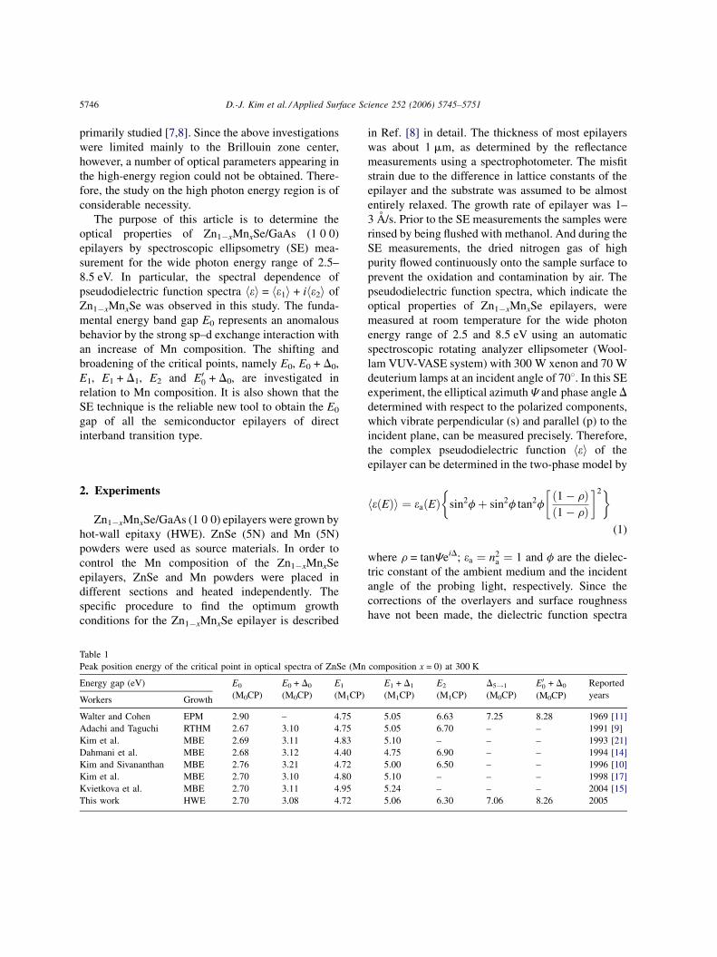
Fig. 1. The pseudodielectric constant e1(E) spectra of Zn1�xMnxSe/
GaAs (1 0 0) epilayers obtained from SE measurement as a function
of Mn composition. The inset represented the oscillation region
below 3.0 eV.
3. Results and discussion
Table 1 shows the critical points determined by a
number of investigators on ZnSe. In the present
study on SE measurement, we have assumed that the
transition occurs in the G-point of Brillouin zone in
ZnSe. It is known that the critical points vary to some
extent according to the crystal growth method. As
delineated in Table 1, our experimental results are
similar to those reported by Adachi and Taguchi [9] at
below 5 eV and those reported by Kim and Siva-
nanthan [10] at above 5 eV. Also, comparing the
CPs reported by Walter and Cohen [11] with those
observed in the present study, the latter yielded the
lower peak position energy values than those of Walter
et al. in entire photon energy range from 2.5 to 8.5 eV.
Also, it is worthy of note that the CPs appearing near
7.0 and 8.26 eV are observed only in our study, as
shown in Table 1.
Figs. 1 and 2 show the pseudodielectric function
spectra hei of Zn1�xMnxSe/GaAs (1 0 0) epilayers
obtained from SE measurement as a function of Mn
composition x. In figures, the arrows represent the
notation of Cardona and Greenaway. The insets of
Figs. 1 and 2 show the shift of E0 peak position in the
oscillation for the photon energy range below 3.0 eV.
The interval of y-axis is widened to observe with
accuracy the shift of E0 peak position. The strong
interference oscillations appearing at the energy below
the energy band gap, E0, are due to the multiple
internal reflections of the light beam in the transparent
epilayer. As listed in Table 1, although there have been
many reports on an E0 peak in Zn1�xMnxSe system
[12,13–15], the data on E0 peak measured by SE as a
function of Mn composition x have not been reported
to date. The optical transitions occurring near G-point
(k = 0) are well known as the E0 gap (G v8!G c
6).
Generally, the energy for direct interband transitions
in semiconductors corresponds to optical energy band
gap, which appears at the right end of oscillation
regions, as shown in Figs. 1 and 2. Choi et al. and Kim
et al. reported the systematic blue-shifting of the E0
gap of Al1�xGaxP and Zn1�xMgxSe as a function of
composition x [16,17]. They also observed the strong
oscillations in the energy region below the E0 gap. In
the same manner, Kim and Sivananthan and Dahmani
et al. reported that the E0 peak in ZnSe appeared at the
right end of oscillation regions [10,14]. The E0 and
E0 + D0 peaks in ZnSe are displayed in the lower
photon energy range and may be related to 3D M0CP
[10]. As shown in Figs. 1 and 2, the E0 gap of pure
ZnSe (x = 0) is 2.70 eV and the E0 for x = 0.05 is
2.67 eV. The E0 + D0 peak by G v7!G c
6 transition
caused by spin–orbit interaction splits near G-point is
distinctly presented at 3.08 eV, especially with lower
Mn composition. However, it was weakened at Mn
composition x = 0.24 and somewhat red-shifted with
increasing Mn composition, and thereafter disap-
peared. Although an intrinsic splitting energy D0 of
approximately 0.4 eVexists in ZnSe, the interval of E0
and E0 + D0 became increasingly smaller owing to the
increased Mn composition [9,12]. Also, the E1 and
E1 + D1 peaks by Lv4;5!Lc
6 and Lv6!Lc
6 transitions
D.-J. Kim et al. / Applied Surface Science 252 (2006) 5745–57515748
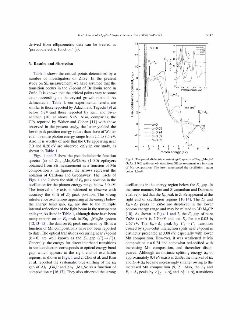
Fig. 2. The pseudodielectric constant e2(E) spectra of Zn1�xMnxSe/
GaAs (1 0 0) epilayers obtained from SE measurement as a function
of Mn composition. The inset represented the oscillation region
below 3.0 eV.
occurring along the L direction near the L-point were
observed near 4.72 and 5.06 eV, respectively. They
can be explained by 3D M1CP type. The peaks show
the red-shifting and broadening with increasing Mn
composition, as shown in Figs. 1 and 2. They were
weakened for higher Mn composition. These results
are qualitatively in good agreement with those
reported by other investigators. Generally, the E1
and E1 + D1 peaks are formed by contribution of
strong 2D exciton in II–VI compounds. However, the
excitons are localized because of the crystalline
degradation or the sp–d hybridization, as the Mn
composition increases [18]. Therefore, the amplitude
of E1 + D1 peak caused by spin–orbit interaction splits
at near L-point decreases to some extent at x = 0.05,
and it merges into a E1 peak as the Mn composition
further increases, shifting the peak to lower energies.
These observations are clearly shown in Figs. 1 and 2.
In general, the splitting energy D1 is known to be
0.3 eV, and our results show the good agreement with
this value [9]. The E2 peak occurred along the S-
direction near the X-point at 6.30 eV, as shown in
Figs. 1 and 2, and is characterized by a damped
harmonic oscillator (DHO) such as the classical
Lorentzian line shape model applied in Adachi’s
report [9]. The E2 peak energy can also be
characterized by strength and damping parameter.
Note that our E2 peak energy value is smaller than that
reported in many other studies [9–11,14]. With
increasing Mn composition x, the rapid decreasing
and red-shifting of the E2 peak intensity was observed,
and then the E2 peak ultimately disappeared above
x = 0.24. The E00 + D0 peak at 8.26 eV caused by 3D
excitons disappeared as Mn composition increased.
This result is due to the low contribution of 3D
excitons of atoms as Mn composition increases. From
the SE measurement in this study, we discovered that
the peak observed around 7.0 eV for the pure ZnSe
epilayer (x = 0) is due to D5!1 transition [11]. This
peak was described in our previous report [8], but it
was not defined in detail. This transition gradually
decreased and completely disappeared at x = 0.24.
Note that the peak is presented in another form near
7.0 eV as the Mn composition x approaches 0.39. This
peak is to due to the spin exchange splitting energy of
Mn 3d+ and the peak increases more distinctly as the
Mn composition x approaches 0.63 [19]. Thus, the
shift and disappearance of these peaks are closely
related to the increase of Mn composition.
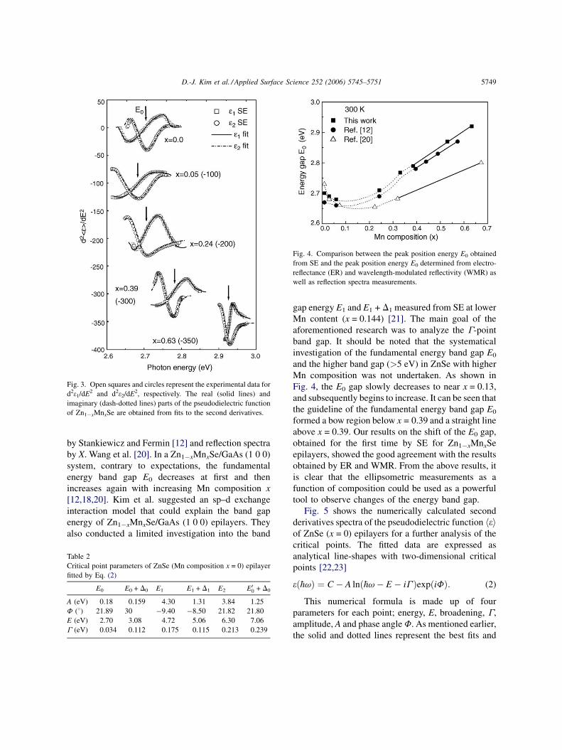
Fig. 3 shows the E0 CPs energies determined by the
second derivative spectra and their fits to Eq. (2) of
pseudodielectric function hei. The results are fitted
using the line shape formula developed by Aspnes
et al. [13]. The solid and dotted lines represent the best
fits and resulting parameters are shown in Table 2.
Note that good agreement between the experimental
data and the fitted data is obtained. These results,
especially, can certify the validity of E0 indicated by
arrows in the inset of Figs. 1 and 2. Also, it can
convince that the energy for direct interband transi-
tions in semiconductors corresponds to optical energy
band gap, which appears at the right end of oscillation
regions.
Fig. 4 compares the peak position energy E0
obtained from SE with the peak position energy E0
determined from electro-reflectance (ER) and wave-
length-modulated reflectivity (WMR) measurements
D.-J. Kim et al. / Applied Surface Science 252 (2006) 5745–5751 5749
Fig. 3. Open squares and circles represent the experimental data for
d2e1/dE2 and d2e2/dE2, respectively. The real (solid lines) and
imaginary (dash-dotted lines) parts of the pseudodielectric function
of Zn1�xMnxSe are obtained from fits to the second derivatives.
Fig. 4. Comparison between the peak position energy E0 obtained
from SE and the peak position energy E0 determined from electro-
reflectance (ER) and wavelength-modulated reflectivity (WMR) as
well as reflection spectra measurements.
by Stankiewicz and Fermin [12] and reflection spectra
by X. Wang et al. [20]. In a Zn1�xMnxSe/GaAs (1 0 0)
system, contrary to expectations, the fundamental
energy band gap E0 decreases at first and then
increases again with increasing Mn composition x
[12,18,20]. Kim et al. suggested an sp–d exchange
interaction model that could explain the band gap
energy of Zn1�xMnxSe/GaAs (1 0 0) epilayers. They
also conducted a limited investigation into the band
Table 2
Critical point parameters of ZnSe (Mn composition x = 0) epilayer
fitted by Eq. (2)
E0 E0 + D0 E1 E1 + D1 E2 E00 + D0
A (eV) 0.18 0.159 4.30 1.31 3.84 1.25
F (8) 21.89 30 �9.40 �8.50 21.82 21.80
E (eV) 2.70 3.08 4.72 5.06 6.30 7.06
G (eV) 0.034 0.112 0.175 0.115 0.213 0.239
gap energy E1 and E1 + D1 measured from SE at lower
Mn content (x = 0.144) [21]. The main goal of the
aforementioned research was to analyze the G-point
band gap. It should be noted that the systematical
investigation of the fundamental energy band gap E0
and the higher band gap (>5 eV) in ZnSe with higher
Mn composition was not undertaken. As shown in
Fig. 4, the E0 gap slowly decreases to near x = 0.13,
and subsequently begins to increase. It can be seen that
the guideline of the fundamental energy band gap E0
formed a bow region below x = 0.39 and a straight line
above x = 0.39. Our results on the shift of the E0 gap,
obtained for the first time by SE for Zn1�xMnxSe
epilayers, showed the good agreement with the results
obtained by ER and WMR. From the above results, it
is clear that the ellipsometric measurements as a
function of composition could be used as a powerful
tool to observe changes of the energy band gap.
Fig. 5 shows the numerically calculated second
derivatives spectra of the pseudodielectric function heiof ZnSe (x = 0) epilayers for a further analysis of the
critical points. The fitted data are expressed as
analytical line-shapes with two-dimensional critical
points [22,23]
eð�hvÞ ¼ C � A lnð�hv� E � iG ÞexpðiFÞ: (2)
This numerical formula is made up of four
parameters for each point; energy, E, broadening, G,
amplitude, A and phase angle F. As mentioned earlier,
the solid and dotted lines represent the best fits and
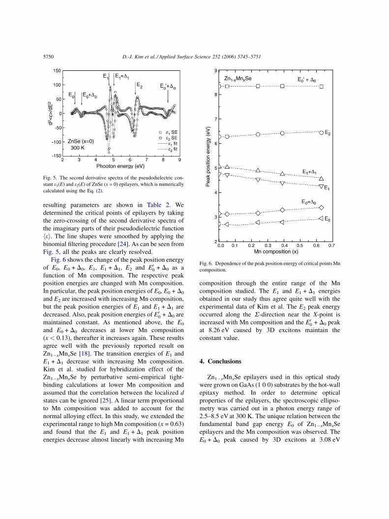
D.-J. Kim et al. / Applied Surface Science 252 (2006) 5745–57515750
Fig. 6. Dependence of the peak position energy of critical points Mn
composition.
Fig. 5. The second derivative spectra of the pseudodielectric con-
stant e1(E) and e2(E) of ZnSe (x = 0) epilayers, which is numerically
calculated using the Eq. (2).
resulting parameters are shown in Table 2. We
determined the critical points of epilayers by taking
the zero-crossing of the second derivative spectra of
the imaginary parts of their pseudodielectric function
hei. The line shapes were smoothed by applying the
binomial filtering procedure [24]. As can be seen from
Fig. 5, all the peaks are clearly resolved.
Fig. 6 shows the change of the peak position energy
of E0, E0 + D0, E1, E1 + D1, E2 and E00 + D0 as a
function of Mn composition. The respective peak
position energies are changed with Mn composition.
In particular, the peak position energies of E0, E0 + D0
and E2 are increased with increasing Mn composition,
but the peak position energies of E1 and E1 + D1 are
decreased. Also, peak position energies of E00 + D0 are
maintained constant. As mentioned above, the E0
and E0 + D0 decreases at lower Mn composition
(x < 0.13), thereafter it increases again. These results
agree well with the previously reported result on
Zn1�xMnxSe [18]. The transition energies of E1 and
E1 + D1 decrease with increasing Mn composition.
Kim et al. studied for hybridization effect of the
Zn1�xMnxSe by perturbative semi-empirical tight-
binding calculations at lower Mn composition and
assumed that the correlation between the localized d
states can be ignored [25]. A linear term proportional
to Mn composition was added to account for the
normal alloying effect. In this study, we extended the
experimental range to high Mn composition (x = 0.63)
and found that the E1 and E1 + D1 peak position
energies decrease almost linearly with increasing Mn
composition through the entire range of the Mn
composition studied. The E1 and E1 + D1 energies
obtained in our study thus agree quite well with the
experimental data of Kim et al. The E2 peak energy
occurred along the S-direction near the X-point is
increased with Mn composition and the E00 + D0 peak
at 8.26 eV caused by 3D excitons maintain the
constant value.
4. Conclusions
Zn1�xMnxSe epilayers used in this optical study
were grown on GaAs (1 0 0) substrates by the hot-wall
epitaxy method. In order to determine optical
properties of the epilayers, the spectroscopic ellipso-
metry was carried out in a photon energy range of
2.5–8.5 eV at 300 K. The unique relation between the
fundamental band gap energy E0 of Zn1�xMnxSe
epilayers and the Mn composition was observed. The
E0 + D0 peak caused by 3D excitons at 3.08 eV
D.-J. Kim et al. / Applied Surface Science 252 (2006) 5745–5751 5751
appeared weakly and then disappeared. The E1 peak
formed at 4.72 eV by the contribution of strong 2D
excitons red-shifted. Also, the weak E1 + D1 peak was
observed at 5.06 eV. The E2 peak caused by DHO at
6.30 eV disappeared as Mn composition x increased.
The E00 + D0 peak located at 8.26 eV was due to 2D
excitons. A peak at approximately 7.0 eV was also
found. This peak due to a D5!1 transition at lower Mn
composition completely disappeared with increasing
Mn composition x. With increasing Mn composition,
another peak caused by the spin exchange splitting
energy of Mn 3d+ showed up near 7.0 eV. Our results
on the shift of the E0 gap determined by SE as a
function of Mn composition x corresponded closely
with the results obtained by ER and WMR. Therefore,
from the SE measurement performed for the first time
in this study for the Zn1�xMnxSe epilayers, it was
clearly seen that the ellipsometric measurements
could be used as a powerful new tool to observe
changes of the energy band gap.
Acknowledgment
This work was supported by a Korea Research
Foundation grant (KRF-2002-070-C00036).
References
[1] J.K. Furdyna, J. Appl. Phys. 64 (1988) 29.
[2] R. Fiederling, M. Keim, G. Reuscher, W. Ossau, G. Schmidt,
A. Waag, L.W. Molenkamp, Nature 402 (1999) 787.
[3] B.T. Jonker, Y.D. Park, B.R. Bennett, H.D. Cheong, G. Kio-
seoglou, A. Petrou, Phys. Rev. B 62 (2001) 8180.
[4] R.M. Stroud, A.T. Hanbicki, Y.D. Park, G. Kioseoglou, A.G.
Petukhov, B.T. Jonker, G. Itskos, A. Petrou, Phys. Rev. Lett. 89
(2002) 166602.
[5] W.M. Chen, I.A. Buyanova, G.Yu. Rudko, A.G. Mal’shukov,
K.A. Chao, A.A. Toropov, Y. Terent’ev, S.V. Sorokin, A.V.
Lebedev, S.V. Ivanov, P.S. Kop’ev, Phys. Rev. B 67 (2003)
125313.
[6] A.A. Toropov, A.V. Lebedev, S.V. Sorokin, D.D. Solnyshkov,
S.V. Ivanov, P.S. Kop’ev, I.A. Buyanova, W.M. Chen, B.
Monemar, Physica E 17 (2003) 352.
[7] T. Matsumoto, A. Ota, K. Nakamura, A. Fujita, Y. Nabetani, T.
Kato, Phys. Status Solidi (c) 1 (2004) 933.
[8] Y.M. Yu, D.J. Kim, K.J. Lee, Y.D. Choi, B.O.K.S. Lee, I.H.
Choi, M.Y. Yoon, J. Vac. Sci. Technol. A 22 (2004) 1908.
[9] S. Adachi, T. Taguchi, Phys. Rev. B 43 (1991) 9569.
[10] C.C. Kim, S. Sivananthan, Phys. Rev. B 53 (1996) 1475.
[11] J.P. Walter, M.L. Cohen, Phys. Rev. 183 (1969) 763.
[12] J. Stankiewicz, J.R. Fermin, J. Appl. Phys. 63 (1988) 3300.
[13] Y.D. Kim, S.L. Cooper, M.V. Klein, B.T. Jonker, Appl. Phys.
Lett. 62 (1993) 2387 (references therein; D.E. Aspnes, in: M.
Balkanski (eds), Handbook on Semiconductors, North-Hol-
land, Amsterdam, 1980, vol. 2, p. 109).
[14] R. Dahmani, L. Salamanca-Riba, N.V. Nguyen, D. Chandler-
Horowitz, B.T. Jonker, J. Appl. Phys. 76 (1994) 514.
[15] J. Kvietkova, B. Daniel, M. Hetterich, M. Schubert, D. Spe-
mann, Thin Solid Films 455–456 (2004) 228.
[16] S.G. Choi, Y.D. Kim, S.D. Yoo, D.E. Aspnes, D.H. Woo, S.H.
Kim, J. Appl. Phys. 87 (2000) 1287.
[17] K.J. Kim, M.H. Lee, J.H. Bahng, C.Y. Kwak, E. Oh, Solid State
Commun. 95 (1997) 17.
[18] W.K. Hung, M.Y. Chern, Y.F. Chen, W.C. Chou, C.S. Yang,
C.C. Cheng, J.L. Shen, Solid State Commun. 120 (2001) 311.
[19] H. Sato, T. Mihara, A. Furuta, Y. Ueda, H. Namatame, M.
Taniguchi, J. Electron Spectrosc. Relat. Phenom. 78 (1996) 87.
[20] X. Wang, X. Chen, J. Liu, C. Chen, J. Wang, Z. Ling, X. Wang,
S. Wang, S. Lu, Solid State Commun. 95 (1995) 525.
[21] Y.D. Kim, S.L. Cooper, M.V. Klein, B.T. Jonker, Phys. Rev. B
49 (1994) 1732.
[22] C.S. Cook, S. Zollner, M.R. Bauer, P. Aella, J. Kouvetakis, J.
Menendez, Thin Solid Films 455–456 (2004) 217.
[23] L. Vina, S. Logothetidis, M. Cardona, Phys. Rev. B30 (1984)
1979.
[24] R. Kellner, J.M. Mermet, M. Otto, H.M. Widmer (Eds.),
Analytical Chemistry, Wiely-Vch, Weinheim, 1998.
[25] Y.D. Kim, S.L. Cooper, M.V. Klein, Phys. Rev. B 48 (1993)
17770.