Embed Size (px)
Citation preview

ELEX 7660: Digital System Design GROUP 5
Navraj Kambo, Brandon Pham 1 of 41 23-Jan-18
ELEX 7660: Digital System Design Group 5 Design Project - FPGA Audio Effects Generator
Brandon Pham, Navraj Kambo
Abstract The FPGA Audio Effects Generator is a project that attempts to utilize the Terasic DE1-SoC development board and System Verilog to generate sound effects hardware. Audio is passed through the system via an auxiliary in/out interface, which joins an audio source and a sink. (In our case, speakers).

ELEX 7660: Digital System Design GROUP 5
Navraj Kambo, Brandon Pham 2 of 41 23-Jan-18
Table of Contents Table of Contents 2
Table of Figures 3
Table of Equations 4
1 Introduction 5
1.1 Motivation 5
1.2 Inspiration 5
2 Background 5
3 System Architecture 6
3.1 Audio Hardware Processor 6
3.1.1 QSYS generated ADC-DAC IP 6
3.1.2 Ready-Valid Handshake, Address Counters, and RAM 8
3.1.3 Echo Effect 12
3.1.4 Tremolo Effect 13
3.2 Effect Controller 14
4 Conclusion 15
5 References 16
6 Code and Quartus Schematics 17
6.1 Audio Hardware Processor Code 17
6.1.1 audiodelay.sv (top-level) 17
6.1.2 chipsel.sv 22
6.1.3 handshake.sv 24
6.1.4 ramctrlc.sv 25
6.1.5 readaddresscounter.sv 27
6.1.6 writeaddresscounter.sv 28
6.1.7 sevensegdecoder.sv 30
6.1.8 delayoutput.sv 31
6.1.9 tencounter.sv 32
6.1.10 sinewave.sv 33
6.1.11 sineedit.sv 35
6.2 Audio Hardware Processor Schematic 37
6.3 Effect Controller Code 38
6.3.1 effectcontrol.sv (top-level) 38

ELEX 7660: Digital System Design GROUP 5
Navraj Kambo, Brandon Pham 3 of 41 23-Jan-18
6.4 Effect Controller Schematic 40
6.5 MATLAB Code 41
Table of Figures Figure 1 - Platform Designer audio module ................................................................................................ 6
Figure 2 - MIKROE-506 breakout board with Wolfson WM7831 audio codec ........................................ 7
Figure 3 - Ready-Valid protocol waveforms, Altera version (left) and UC Berkeley version (right) ........ 9
Figure 4 - Chip select testbench before modification ................................................................................. 9
Figure 5 - Chip select testbench waveforms ............................................................................................. 10
Figure 6 - Address counter testbench waveforms ..................................................................................... 11
Figure 7 - Signal flow graph of Equation 3 ............................................................................................... 12
Figure 8 - Sinewave generator module testbench ..................................................................................... 13
Figure 9 - Wiring diagram for the effect controller .................................................................................. 14
Figure 10 - audiodelay.sv code(1) (top-level) ........................................................................................... 17
Figure 11 - audiodelay.sv code(2) (top-level) ........................................................................................... 18
Figure 12 - audiodelay.sv code(3) (top-level) ........................................................................................... 19
Figure 13 - audiodelay.sv code(4) (top-level) ........................................................................................... 20
Figure 14 - audiodelay.sv code(5) (top-level) ........................................................................................... 21
Figure 15 - chipsel.sv code ........................................................................................................................ 22
Figure 16 – chipse_tb.sv code ................................................................................................................... 23
Figure 17 – handshake.sv code ................................................................................................................. 24
Figure 18 – ramctrlc.sv code(1) ................................................................................................................ 25
Figure 19 – ramctrlc.sv code(2) ................................................................................................................ 26
Figure 20 – readaddresscounter.sv code ................................................................................................... 27
Figure 21 – writeaddresscounter.sv code .................................................................................................. 28
Figure 22 – write_tb.sv code ..................................................................................................................... 29
Figure 23 – sevensegdecoder.sv code ....................................................................................................... 30
Figure 24 – delayoutput.sv code(1) ........................................................................................................... 31
Figure 25 – delayoutput.sv code(2) ........................................................................................................... 32
Figure 26 – tencounter.sv code ................................................................................................................. 32
Figure 27 – sinewave.sv code(1) ............................................................................................................... 33
Figure 28 – sinewave.sv code(2) ............................................................................................................... 34
Figure 29 – sineedit.sv code ...................................................................................................................... 35
ELEX 7660: Digital System Design GROUP 5
Navraj Kambo, Brandon Pham 4 of 41 23-Jan-18
Figure 29 – tencounter_tb.sv code ............................................................................................................ 36
Figure 30 - Top level schematic audio hardware processor without effects ............................................. 37
Figure 31 - effectcontrol.sv code(1) (top-level) ........................................................................................ 38
Figure 32 - effectcontrol.sv code(2) (top-level) ........................................................................................ 39
Figure 33 - effectcontrol.sv code(3) (top-level) ........................................................................................ 40
Figure 34 - Effect controller schematic ..................................................................................................... 40
Figure 35 - matlabfx.m code ..................................................................................................................... 41
Table of Equations Equation 1 - Single echo sound effect relationship ................................................................................... 12
Equation 2 - Multiple echoes sound effect using multiple feedback paths ............................................... 12
Equation 3 - Multiple echoes sound effect using single feedback path .................................................... 12
Equation 4 - Tremolo Effect relationship .................................................................................................. 13

ELEX 7660: Digital System Design GROUP 5
Navraj Kambo, Brandon Pham 5 of 41 23-Jan-18
1 Introduction 1.1 Motivation
This project was in part inspired by our passion for musical production, while also exploring the realm of signal processing. Growing up listening to a plethora of different musical producers, we’ve had the chance to experience and understand audio effects, and their place in music. When we first were given this assignment, it was established early that we would be exploring music in one form or another. Our first idea was based synthesizing sounds similar to the Roland TR-808 drum machine, however this task seemed too complex for our allotted time. We decided instead to alter instead of source audio, due to our time constraints.
1.2 Inspiration Past projects have been centered on real time audio effects processing and were used as a source of inspiration. Said projects, such as the FPGA Implementation of Audio Effects project by students of the University of Alberta were used as reference material, and a base for our project. The project also provided some insight into the implementation of such effects. To better understand the signal processing aspect of our project, we found a tutorial which walked through some common sound effects using MATLAB. The effects were implemented similar to how they would be in hardware, which made the conversion easy.
2 Background Audio effects are used in nearly all applications that involves music or sound of some sort,
whether it's in live concert performances, video game soundtracks, or television shows, it’s almost certain that an audio effect of some kind is being used. So, what are audio effects? Audio effects, also known as sound effects, are software or hardware generated sounds or sound processes used to modify or add depth to an audio signal. These effects vary, and they are organized based on the parameter of the audio signal that they modify, such as amplitude, time-based, spectral, and dynamic effects.

ELEX 7660: Digital System Design GROUP 5
Navraj Kambo, Brandon Pham 6 of 41 23-Jan-18
3 System Architecture 3.1 Audio Hardware Processor To have the system perform as expected, we needed to generate hardware based on how certain effects would operate. Our main goal for this project was to create echo and tremolo effects in hardware. Each of the effects were first coded and analysed in MATLAB, and then were designed using the MATLAB code as a reference. Luckily, a document published by Cardiff University [1] explains a plethora of audio DSP effects using MATLAB, which we found useful.
3.1.1 QSYS generated ADC-DAC IP In order to sample and write data, we needed to initialize the Terasic DE1-SoC audio codec. This can be done using the Quartus Prime Platform Designer, which includes all the necessary IP for initializing the codec, including the ADC and DAC IP, the codec initialization IP and the audio PLL required to operate the codec. These components can be interconnected in Platform Designer to be instantiated as a single module, needed later in the project. A useful tutorial for creating this module can be found in a lab tutorial provided by University of Cambridge [2], which walks through the Platform Designer setup and requirements, including connections shown below in Figure 1. When initializing the codec in Platform Designer, the following settings were selected in the wizard;
● Avalon Type: Streaming ● Data Width: 24 bits ● Audio-in path: Line-in to ADC ● Sampling Rate: 48kHz ● Audio Clock Frequency: 12.288MHz
Figure 1 - Platform Designer audio module
The codec on board the DE1-SoC is the Wolfson WM8731 codec, which includes a 24-bit sigma delta DAC and ADC. From the datasheet [3] provided by Altera regarding the DE1-SoC and the Wolfson Audio Codec [4], internal signals which were exported from Platform Designer were matched to those on the codec, giving rise to the appropriate pins being assigned in Quartus, via the Assignment Editor. Some of the important signals to consider include, but are not limited to the following;
● SCLK - Serial interface clock ● ADCLRC - ADC left-right channel clock ● DACLRC - DAC left-right channel clock ● ADCDAT - Data coming out of ADC on serial interface ● DACDAT - Data going into DAC on serial interface ● BCLK - Bit clock ● XCLK - PLL generated clock to codec (12.288MHz)

ELEX 7660: Digital System Design GROUP 5
Navraj Kambo, Brandon Pham 7 of 41 23-Jan-18
It’s important to note that although this project was carried out on an Terasic DE1-SoC, it could be carried out on an Terasic DE0 FPGA as well. The only caveat being that due to the lack of a built-in audio codec, an external codec such as the one shown in Figure 2, can be would need to be interfaced. A breakout board with Wolfson WM8731 would be the most ideal solution due to IP already available in Quartus, however other audio codecs may also have IP written. Implementation in hardware is exactly the same as it would be with the built-in audio codec on the Terasic DE1-SoC.
Figure 2 - MIKROE-506 breakout board with Wolfson WM7831 audio codec

ELEX 7660: Digital System Design GROUP 5
Navraj Kambo, Brandon Pham 8 of 41 23-Jan-18
3.1.2 Ready-Valid Handshake, Address Counters, and RAM Using the audio codec with the IP supplied in Quartus required a handshake between hardware
interfaces, such as the ADC and DAC interface. This wasn’t a problem with a straight-through connection, where the ADC was connected directly to the DAC, because both interfaces had the correct signals to ensure their connection. However, this was not the case when interfacing with other Quartus IP such as 2-port RAM, which uses enable signals instead of hand shakes, and is needed for some memory-based audio effects. A hardware module was needed to fill the gap between the two hardware interfaces, that would be able to facilitate the transfer of data correctly between the codec and RAM.
Initially, we decided that we could possibly edit a FIFO buffer module previously written, which already employed the Ready-Valid interface, but this seemed to stem its own problems. For starters, the FIFO buffer needed to be modified so that it could be used as a ring buffer, where an external tap would control which memory address was being read from. In addition to this, the buffer would need to be able to accommodate a second of data. Using equation 2 and the fact we were sampling at 48kHz, we were able to determine that a depth of 6000 words was needed. Also, since we had a 24-bit wide bus, this meant we needed to have at least 1.152 million bits of memory allocated, which was greater than the maximum size in Quartus.
𝐷𝑒𝑝𝑡ℎ = 𝑓𝑠𝑎𝑚𝑝 ∗ 𝐷𝑒𝑙𝑎𝑦𝑀𝑎𝑥 Equation 2 - Buffer depth and sample frequency relationship.
In the end, what was decided was that we should’ve used 3 2-port RAM modules which had depths of 2048 words, and have some sort of interface circuitry to be able to handle addressing. This gave rise to the chip select module coded in Verilog, whose purpose was to be able to direct 16-bit read and write addresses into 14-bit addresses for the appropriate RAM chip, as well as toggle the enable pins on the respective RAM chip. The chip select module works in conjunction with the hand shake module, which converts the Ready-Valid interface into a simpler enable interface. To better understand how the Ready-Valid interface actually works, we looked at some notes from UC Berkeley College of Engineering [5] on this topic, which were both helpful and misleading. They were helpful in the sense that they explained how the data is transferred only when both ready and valid signals are asserted, but what they neglected to mention was that they were basing their notes on a specific version of the protocol. Altera uses a version of the protocol which starts with initiation of the ready signal, unlike the UC Berkeley version which starts with a high, valid signal. Also, information regarding the Ready-Valid protocol is hidden deep inside of a document provided by Altera, titled “Avalon Interface Specifications” [6], which is not included in the documentation of the audio interface IP. Below, Figure 3 shows the difference between the two versions of the protocol, including the enable and address signals which are used in our modules. The black signals are driven by interfaces, while the blue signals are derived from the modules. It’s important to note that we designed based on the UC Berkeley specifications instead of those provided by Altera, which caused come connection issues.

ELEX 7660: Digital System Design GROUP 5
Navraj Kambo, Brandon Pham 9 of 41 23-Jan-18
Figure 3 - Ready-Valid protocol waveforms, Altera version (left) and UC Berkeley version (right)
Although our hand shake module is incorrect, we’ve included a testbench and its output in this report, shown in Figure 4. Initially, the testbench waveform showed a write address counter incrementing through addresses which would be written to during simulation.
Figure 4 - Chip select testbench before modification
The testbench was edited to accommodate more signals later during the project, and to show when the RAM modules would be read from and written to. The output waveforms for this edited testbench are displayed in Figure 5.

ELEX 7660: Digital System Design GROUP 5
Navraj Kambo, Brandon Pham 10 of 41 23-Jan-18
Figure 5 - Chip select testbench waveforms
A separate RAM address counter testbench was created, for separately debugging the RAM address read and write counters. These counter modules are used to provide the RAM controller module a 16-bit address to read from or write to. The addresses are then broken up by the RAM controller module into separate 14 bit addresses to be used with the RAM modules. This module is used mainly to control the delay between feedback and input, by setting the read pointer an integer number of addresses away. This is discussed more in depth in the

ELEX 7660: Digital System Design GROUP 5
Navraj Kambo, Brandon Pham 11 of 41 23-Jan-18
3.1.3 Echo Effect portion of the report, and the testbench for this module is provided in the appendix, with the waveforms shown in Figure.
Figure 6 - Address counter testbench waveforms
After 48000 addresses have been written to, a count full signal latches, causes the read address counter to begin incrementing with the write address counter. This ensures that delays will only occur once the RAM has been filled. All testbenches and code for this section of the report can be found in the appendix of this report.
ELEX 7660: Digital System Design GROUP 5
Navraj Kambo, Brandon Pham 12 of 41 23-Jan-18
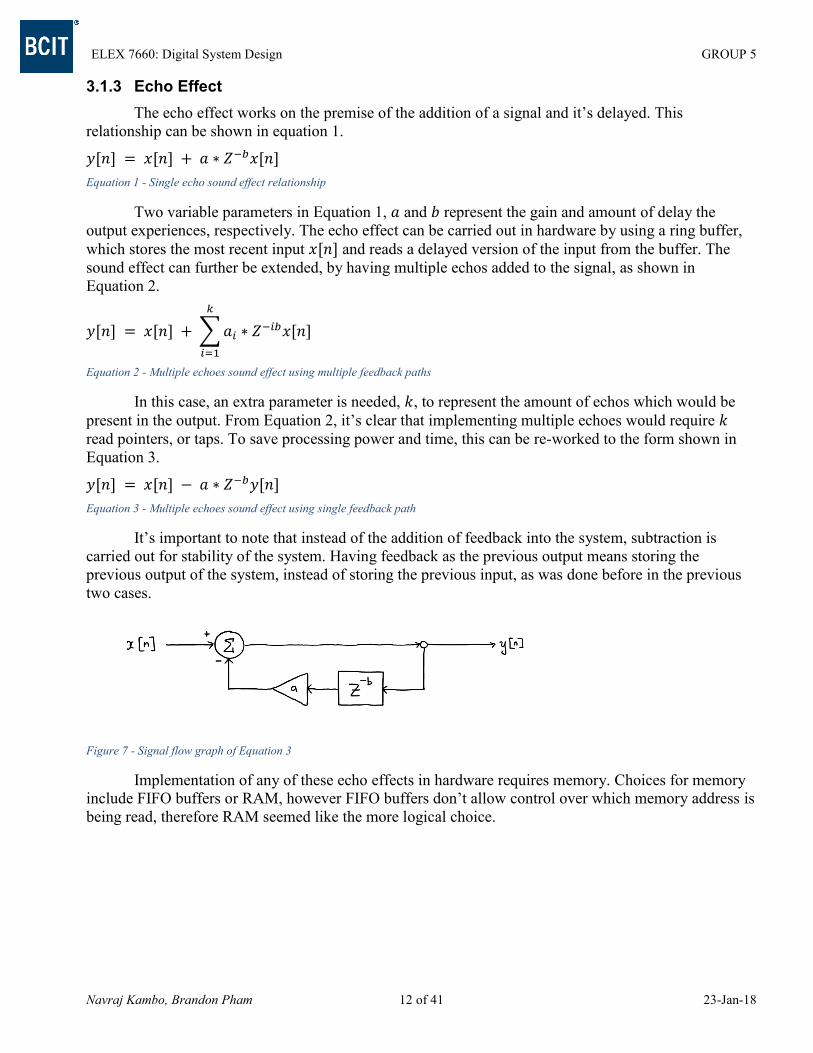
3.1.3 Echo Effect The echo effect works on the premise of the addition of a signal and it’s delayed. This relationship can be shown in equation 1.
𝑦[𝑛] = 𝑥[𝑛] + 𝑎 ∗ 𝑍−𝑏𝑥[𝑛] Equation 1 - Single echo sound effect relationship
Two variable parameters in Equation 1, 𝑎 and 𝑏 represent the gain and amount of delay the output experiences, respectively. The echo effect can be carried out in hardware by using a ring buffer, which stores the most recent input 𝑥[𝑛] and reads a delayed version of the input from the buffer. The sound effect can further be extended, by having multiple echos added to the signal, as shown in Equation 2.
𝑦[𝑛] = 𝑥[𝑛] + ∑ 𝑎𝑖 ∗ 𝑍−𝑖𝑏𝑥[𝑛]
𝑘
𝑖=1
Equation 2 - Multiple echoes sound effect using multiple feedback paths
In this case, an extra parameter is needed, 𝑘, to represent the amount of echos which would be present in the output. From Equation 2, it’s clear that implementing multiple echoes would require 𝑘 read pointers, or taps. To save processing power and time, this can be re-worked to the form shown in Equation 3.
𝑦[𝑛] = 𝑥[𝑛] − 𝑎 ∗ 𝑍−𝑏𝑦[𝑛] Equation 3 - Multiple echoes sound effect using single feedback path
It’s important to note that instead of the addition of feedback into the system, subtraction is carried out for stability of the system. Having feedback as the previous output means storing the previous output of the system, instead of storing the previous input, as was done before in the previous two cases.
Figure 7 - Signal flow graph of Equation 3
Implementation of any of these echo effects in hardware requires memory. Choices for memory include FIFO buffers or RAM, however FIFO buffers don’t allow control over which memory address is being read, therefore RAM seemed like the more logical choice.

ELEX 7660: Digital System Design GROUP 5
Navraj Kambo, Brandon Pham 13 of 41 23-Jan-18
3.1.4 Tremolo Effect The tremolo effect is essentially amplitude modulation, which varies the max level of the input. The relationship for the effect is shown in Equation 4.
𝑦[𝑛] = (1 + 𝑎 ∗ sin[Ω𝑡𝑛]) ∗ 𝑥[𝑛] Equation 4 - Tremolo Effect relationship
The two parameters, Ω𝑡 and 𝑎, are the tremolo and gain of the effect respectively. The tremolo frequency in in Hz, and is usually a low frequency, while the gain is usually less than 1. Creating this effect in hardware took some creativity, and experience with MATLAB. Since there isn’t a sinewave function in Verilog, a sinewave module needed to be constructed. While researching this problem, we encountered two interesting solutions, using the CORDIC algorithm, or creating a look up table (LUT). The CORDIC algorithm allowed us to create sinewaves with precise values, but the implication with the CORDIC algorithm was that it took processing time. Matrix manipulation on the FPGA could take precious time away, and since we were working on a real time system, this seemed rather risky.
Instead we decided to generate a LUT for a sinewave. This was done in MATLAB, by creating a vector that was 100 samples long, and then running the vector through a sine function. The sine function was then scaled, so that it’s peak amplitude reached a max value of 16, and a minimum value of 0. A separate module was then created, whose sole purpose was to add a scalar of 16, so that the net effect would result in a sinewave with a gain of 1, which was multiplied by a scalar of 16. This multiplication could later be undone, by shifting 4 bits to the right, saving processing power and time.
The end goal of this whole ordeal was to produce a quarter of the period of a sinewave in 100 samples, so that we could generate a LUT which was efficient with respect to memory usage. However, the trade off was that our logic needed to be able to know when and how to effectively flip the LUT coefficients, so that a full sinewave could be produced. We were able to design and simulate a set of modules which accomplished this task, including a testbench shown in Figure 8.
Figure 8 - Sinewave generator module testbench
ELEX 7660: Digital System Design GROUP 5
Navraj Kambo, Brandon Pham 14 of 41 23-Jan-18
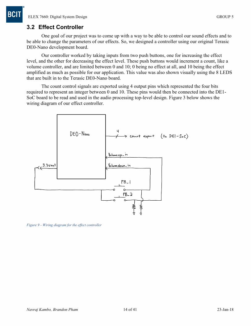
3.2 Effect Controller One goal of our project was to come up with a way to be able to control our sound effects and to be able to change the parameters of our effects. So, we designed a controller using our original Terasic DE0-Nano development board.
Our controller worked by taking inputs from two push buttons, one for increasing the effect level, and the other for decreasing the effect level. These push buttons would increment a count, like a volume controller, and are limited between 0 and 10; 0 being no effect at all, and 10 being the effect amplified as much as possible for our application. This value was also shown visually using the 8 LEDS that are built in to the Terasic DE0-Nano board.
The count control signals are exported using 4 output pins which represented the four bits required to represent an integer between 0 and 10. These pins would then be connected into the DE1-SoC board to be read and used in the audio processing top-level design. Figure 3 below shows the wiring diagram of our effect controller.
Figure 9 - Wiring diagram for the effect controller

ELEX 7660: Digital System Design GROUP 5
Navraj Kambo, Brandon Pham 15 of 41 23-Jan-18
4 Conclusion This project was a great way to show off what we’ve learned in ELEX 7660, while providing an opportunity to learn on our own. It really gave us the chance to experiencing the kinds of problems hardware designers have to face in terms of interfacing components, and generally making things work together as they should. Unfortunate, we were not able to provide sound effects as we had hoped, due to problems and limited documentation on the Quartus IP, however we were able to make a leap in the right direction. Hardware for this project can be salvaged, and hopefully someone in the future will continue with what we have laid out.
Also, we feel as though other groups can learn from our mistakes. Having put aside this project with respect to other classwork, it’s possible that we could’ve put more time into the project overall, or started earlier. We hope that our project will help others struggling with the Ready-Valid interface problem in Quartus, as well as provide general information on the Quartus Audio IP core.
Some future work which can be carried out includes, adding the effects into the top level, and coding a convolution reverb using the Quartus FFT IP core.

ELEX 7660: Digital System Design GROUP 5
Navraj Kambo, Brandon Pham 16 of 41 23-Jan-18
5 References
[1]
Cardiff University, "10_CM0268_Audio_FX.pdf," [Online]. Available: http://users.cs.cf.ac.uk/Dave.Marshall/CM0268/PDF/10_CM0268_Audio_FX.pdf. [Accessed 12 February 2018].
[2]
S. Moore, "Computer Laboratory - Courses 2016–17 - ECAD and Architecture Practical Classes - Tutorial," University of Cambridge, 2016. [Online]. Available: https://www.cl.cam.ac.uk/teaching/1617/ECAD+Arch/optional-tonegen.html. [Accessed 22 March 2018].
[3]
Intel Corporation, "Intel FPGA University Program Audio core," [Online]. Available: ftp://ftp.altera.com/up/pub/Intel_Material/16.1/University_Program_IP_Cores/Audio_Video/Audio.pdf. [Accessed 12 February 2018].
[4]
Wolfson Microelectronics, "WM8731/WM8731L," 2010. [Online]. Available: http://www.cs.columbia.edu/~sedwards/classes/2012/4840/Wolfson-WM8731-audio-CODEC.pdf. [Accessed 10 March 2018].
[5]
C. Fletcher, "Interfaces.pdf," 24 February 2009. [Online]. Available: https://inst.eecs.berkeley.edu/~cs150/Documents/Interfaces.pdf. [Accessed 22 March 2018].
[6]
Intel Corporation, "Avalon® Interface Specifications," 3 March 2018. [Online]. Available: https://www.altera.com/content/dam/altera-www/global/en_US/pdfs/literature/manual/mnl_avalon_spec.pdf. [Accessed 22 March 2018].

ELEX 7660: Digital System Design GROUP 5
Navraj Kambo, Brandon Pham 17 of 41 23-Jan-18
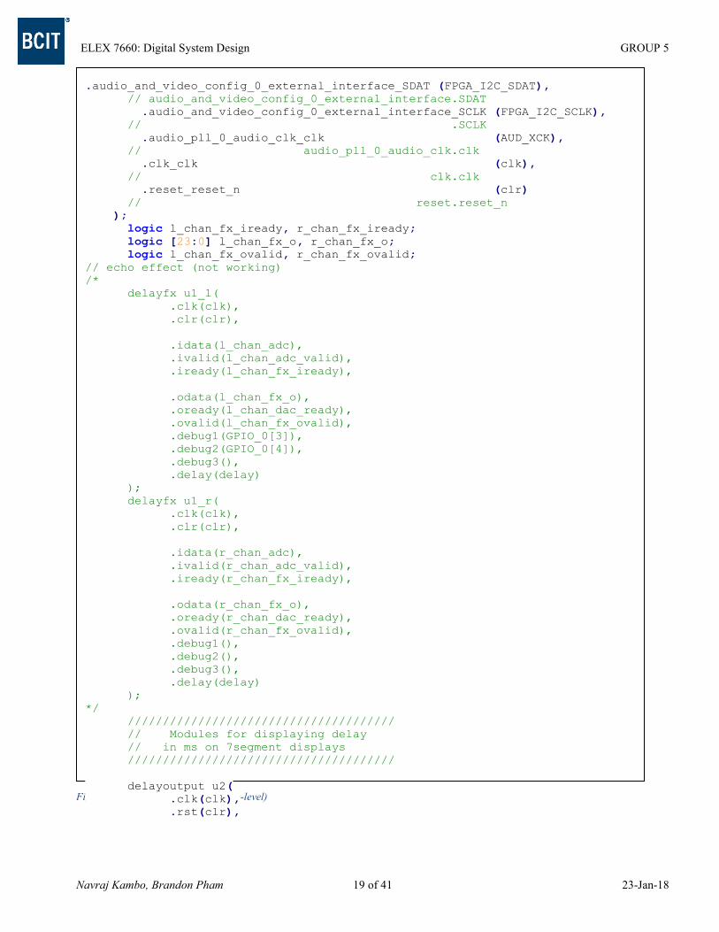
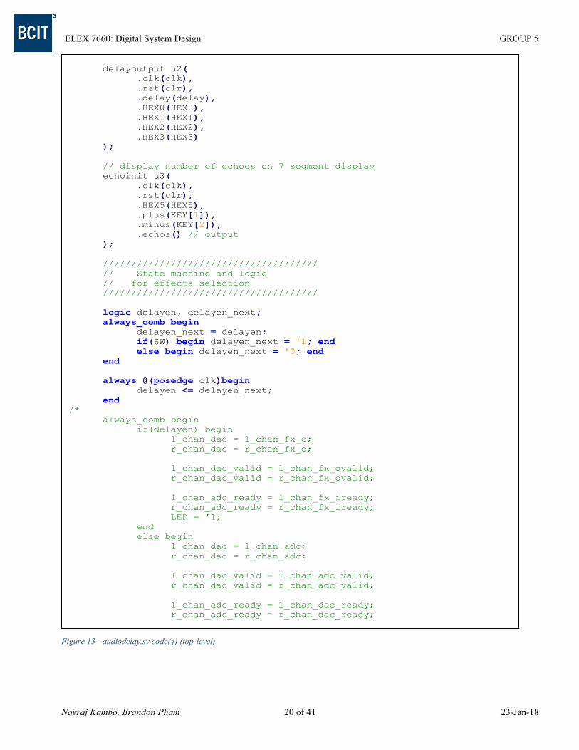
6 Code and Quartus Schematics 6.1 Audio Hardware Processor Code 6.1.1 audiodelay.sv (top-level)
Figure 10 - audiodelay.sv code(1) (top-level)
// audiodelay.sv - ELEX 7660 201810 top level entity of project
//
// Navraj Kambo A00###### 2018-3-10
module audiodelay(
CLOCK_50,
SW,
KEY, // AA14, AA15, W15
LED,
AUD_ADCDAT,
AUD_ADCLRCK,
AUD_BCLK,
AUD_DACDAT,
AUD_DACLRCK,
FPGA_I2C_SDAT,
FPGA_I2C_SCLK,
AUD_XCK,
HEX5, // V25, AA28, Y27, AB27, AB26, AA26, AA25
HEX0, // AE26, AE27, AE28, AG27, AF28, AG28, AH28
HEX1, // AJ29, AH29, AH30, AG30, AF29, AF30, AD27
HEX2, // AB23, AE29, AD29, AC28, AD30, AC29, AC30
HEX3, // AD26, AC27, AD25, AC25, AB28, AB25, AB22
GPIO_0
);
/////////////////////////////////////////
// FPGA internal connections
////////////////////////////////////////
input AUD_ADCDAT;
input SW;
input [2:0] KEY;
output [6:0] HEX0, HEX1, HEX2, HEX3, HEX5;
input CLOCK_50;
input AUD_BCLK;
input AUD_ADCLRCK;
input AUD_DACLRCK;
inout FPGA_I2C_SDAT;
output AUD_XCK;
output FPGA_I2C_SCLK;
output AUD_DACDAT;
output LED;
logic clk;
output logic [4:0] GPIO_0;
//////////////////////////////////////
// FPGA assorted signals
//////////////////////////////////////
assign clk = CLOCK_50;
logic [23:0] l_chan_adc, r_chan_adc, l_chan_dac, r_chan_dac ;
logic l_chan_adc_valid, r_chan_adc_valid, l_chan_dac_valid, r_chan_dac_valid;
logic l_chan_adc_ready, r_chan_adc_ready, l_chan_dac_ready, r_chan_dac_ready;
logic clr;
assign clr = KEY[0];

ELEX 7660: Digital System Design GROUP 5
Navraj Kambo, Brandon Pham 18 of 41 23-Jan-18
Figure 11 - audiodelay.sv code(2) (top-level)
logic [23:0] l_chan_fx, r_chan_fx; logic l_chan_fx_ready, r_chan_fx_ready, l_chan_fx_valid, r_chan_fx_valid; logic [4:0] delay = 'd10;
///////////////////////////////////////////
// Debug
///////////////////////////////////////////
assign GPIO_0[0] = AUD_ADCDAT; assign GPIO_0[1] = AUD_DACDAT; assign GPIO_0[2] = AUD_XCK; //assign GPIO_0[3] = '1;
//assign GPIO_0[4] = '1;
//assign GPIO_0[5] = ;
//assign GPIO_0[6] = ;
////////////////////////////////////// // FPGA module instantiations ////////////////////////////////////// // platform designer module audiointerface u0 ( .audio_0_avalon_left_channel_source_data (l_chan_adc), //
audio_0_avalon_left_channel_sink.data .audio_0_avalon_left_channel_source_valid (l_chan_adc_valid), //
.valid
.audio_0_avalon_left_channel_source_ready (l_chan_adc_ready), //
.ready
.audio_0_avalon_left_channel_sink_ready (l_chan_dac_ready), //
audio_0_avalon_left_channel_source.ready .audio_0_avalon_left_channel_sink_data (l_chan_dac), //
.data
.audio_0_avalon_left_channel_sink_valid (l_chan_dac_valid), //
.valid
.audio_0_avalon_right_channel_source_data (r_chan_adc), //
audio_0_avalon_right_channel_sink.data .audio_0_avalon_right_channel_source_valid (r_chan_adc_valid), //
.valid
.audio_0_avalon_right_channel_source_ready (r_chan_adc_ready), //
.ready
.audio_0_avalon_right_channel_sink_ready (r_chan_dac_ready), //
audio_0_avalon_right_channel_source.ready .audio_0_avalon_right_channel_sink_data (r_chan_dac), //
.data
.audio_0_avalon_right_channel_sink_valid (r_chan_dac_valid), //
.valid
.audio_0_external_interface_ADCDAT (AUD_ADCDAT), //
audio_0_external_interface.ADCDAT .audio_0_external_interface_ADCLRCK (AUD_ADCLRCK), //
.ADCLRCK
.audio_0_external_interface_BCLK (AUD_BCLK), //
.BCLK
.audio_0_external_interface_DACDAT (AUD_DACDAT), //
.DACDAT
.audio_0_external_interface_DACLRCK (AUD_DACLRCK), //
.DACLRCK
ELEX 7660: Digital System Design GROUP 5
Navraj Kambo, Brandon Pham 19 of 41 23-Jan-18
Figure 12 - audiodelay.sv code(3) (top-level)
.audio_and_video_config_0_external_interface_SDAT (FPGA_I2C_SDAT),
// audio_and_video_config_0_external_interface.SDAT .audio_and_video_config_0_external_interface_SCLK (FPGA_I2C_SCLK),
// .SCLK .audio_pll_0_audio_clk_clk (AUD_XCK),
// audio_pll_0_audio_clk.clk .clk_clk (clk),
// clk.clk .reset_reset_n (clr)
// reset.reset_n ); logic l_chan_fx_iready, r_chan_fx_iready; logic [23:0] l_chan_fx_o, r_chan_fx_o; logic l_chan_fx_ovalid, r_chan_fx_ovalid; // echo effect (not working)
/*
delayfx u1_l(
.clk(clk),
.clr(clr),
.idata(l_chan_adc),
.ivalid(l_chan_adc_valid),
.iready(l_chan_fx_iready),
.odata(l_chan_fx_o),
.oready(l_chan_dac_ready),
.ovalid(l_chan_fx_ovalid),
.debug1(GPIO_0[3]),
.debug2(GPIO_0[4]),
.debug3(),
.delay(delay)
);
delayfx u1_r(
.clk(clk),
.clr(clr),
.idata(r_chan_adc),
.ivalid(r_chan_adc_valid),
.iready(r_chan_fx_iready),
.odata(r_chan_fx_o),
.oready(r_chan_dac_ready),
.ovalid(r_chan_fx_ovalid),
.debug1(),
.debug2(),
.debug3(),
.delay(delay)
);
*/ ////////////////////////////////////// // Modules for displaying delay // in ms on 7segment displays //////////////////////////////////////
delayoutput u2( .clk(clk), .rst(clr),
ELEX 7660: Digital System Design GROUP 5
Navraj Kambo, Brandon Pham 20 of 41 23-Jan-18
Figure 13 - audiodelay.sv code(4) (top-level)
delayoutput u2( .clk(clk), .rst(clr), .delay(delay), .HEX0(HEX0), .HEX1(HEX1), .HEX2(HEX2), .HEX3(HEX3) );
// display number of echoes on 7 segment display echoinit u3( .clk(clk), .rst(clr), .HEX5(HEX5), .plus(KEY[1]), .minus(KEY[2]), .echos() // output );
////////////////////////////////////// // State machine and logic // for effects selection //////////////////////////////////////
logic delayen, delayen_next; always_comb begin delayen_next = delayen; if(SW) begin delayen_next = '1; end else begin delayen_next = '0; end end
always @(posedge clk)begin delayen <= delayen_next; end /*
always_comb begin
if(delayen) begin
l_chan_dac = l_chan_fx_o;
r_chan_dac = r_chan_fx_o;
l_chan_dac_valid = l_chan_fx_ovalid;
r_chan_dac_valid = r_chan_fx_ovalid;
l_chan_adc_ready = l_chan_fx_iready;
r_chan_adc_ready = r_chan_fx_iready;
LED = '1;
end
else begin
l_chan_dac = l_chan_adc;
r_chan_dac = r_chan_adc;
l_chan_dac_valid = l_chan_adc_valid;
r_chan_dac_valid = r_chan_adc_valid;
l_chan_adc_ready = l_chan_dac_ready;
r_chan_adc_ready = r_chan_dac_ready;

ELEX 7660: Digital System Design GROUP 5
Navraj Kambo, Brandon Pham 21 of 41 23-Jan-18
Figure 14 - audiodelay.sv code(5) (top-level)
LED = '0;
end
end
// set straight through connection from ADC to DAC for debugging purposes
assign l_chan_dac = l_chan_adc; assign r_chan_dac = r_chan_adc;
assign l_chan_adc_ready = l_chan_dac_ready; assign r_chan_adc_ready = r_chan_dac_ready;
assign l_chan_dac_valid = l_chan_adc_valid; assign r_chan_dac_valid = r_chan_adc_valid; assign LED = '1;
endmodule

ELEX 7660: Digital System Design GROUP 5
Navraj Kambo, Brandon Pham 22 of 41 23-Jan-18
6.1.2 chipsel.sv
Figure 15 - chipsel.sv code
// chipsel.sv - ELEX 7660 201810 selects 1 of 3 RAM chips based on the read
// and write address inputs, converts the Ready-Valid interface for the RAM
// chips into enable signals, and converts 16 bit addresses into 14 bit
// addresses
// Navraj Kambo A00###### 2018-3-20
module chipsel(
input logic [15:0] writeaddress, readaddress,
input logic iready, ovalid, cntfull,
output logic [13:0] cwaddr, craddr,
output logic [2:0] wen, ren
);
logic [2:0] write, read;
assign wen = write;
assign ren = read;
always_comb begin
if(iready) begin
if(writeaddress < 'd16384) write = 3'b001;
else if(writeaddress >= 'd16384 && writeaddress < 'd32768)
write = 3'b010;
else write = 3'b010;
end
else write = 3'b000;
end
always_comb begin
unique case(write)
3'b001: cwaddr = writeaddress;
3'b010: cwaddr = writeaddress - 'd16384;
3'b100: cwaddr = writeaddress - 'd32768;
3'b000: cwaddr = '0;
endcase
end
always_comb begin
if(ovalid && cntfull) begin
if(readaddress < 'd16384) read = 3'b001;
else if(readaddress >= 'd16384 && readaddress < 'd32768)
read = 3'b010;
else read = 3'b010;
end
else if(ovalid) begin
read = 3'b000;
end
else read = 3'b000;
end
always_comb begin
unique case(read)
3'b001: craddr = readaddress;
3'b010: craddr = readaddress - 'd16384;
3'b100: craddr = readaddress - 'd32768;
3'b000: craddr = '0;
endcase
end
endmodule

ELEX 7660: Digital System Design GROUP 5
Navraj Kambo, Brandon Pham 23 of 41 23-Jan-18
Figure 16 – chipse_tb.sv code
// chipsel_tb.sv - ELEX 7660 201810 testbench for memory interfaces used in
// echo effects
// Navraj Kambo A00###### 2018-4-02
module chipsel_tb();
writeaddresscounter wcnt(.*);
readaddresscounter rcnt(.*);
chipsel ram(.*);
handshake interf(.*);
logic clk, clk_48k, clk_50m, rst;
logic [3:0] delay = 'd1;
logic ivalid, cntfull, iready, ovalid, oready;
logic [15:0] writeaddress, readaddress;
logic [16:0] i;
logic [13:0] cwaddr, craddr;
logic [2:0] wen, ren;
assign clk = clk_50m;
initial begin
rst = '0;
// generate reset signal
#20ns rst = '1;
#40ns begin rst = '0; end
end
initial begin
clk_50m = '1;
forever begin
#10ns clk_50m = ~clk_50m;
end
end
initial begin
clk_48k = '1;
forever begin
#10.4166us clk_48k = ~clk_48k;
end
end
initial begin
@(negedge rst) begin
for (i=0; i<65538; i=i+1) begin
ivalid = '1;
#10.4166us ivalid = '0;
#10.4166us ;
end
$stop;
end
end
always @(posedge ovalid) begin
oready = '0;
#2.208us oready = '1;
#2.208us oready = '0;
end
endmodule

ELEX 7660: Digital System Design GROUP 5
Navraj Kambo, Brandon Pham 24 of 41 23-Jan-18
6.1.3 handshake.sv
Figure 17 – handshake.sv code
// handshake.sv - ELEX 7660 201810 generates ready and valid signals for ADC
// and DAC based on RAM enable signals
// Navraj Kambo A00###### 2018-4-10
module handshake(
input logic clk, rst,
input logic ivalid, oready,
output logic iready, ovalid
);
logic iready_next, ivalid_prev, ovalid_next, oready_prev;
logic cycleflg, cycleflg_next, outflg, outflg_next;
always_comb begin
if(rst) begin
iready_next = '0;
cycleflg_next = '0;
end
else begin
iready_next = iready;
cycleflg_next = cycleflg;
if(ivalid && ~ovalid && ~iready && ~cycleflg) begin
iready_next = '1; cycleflg_next = '1; end
if(ivalid && ~ovalid && iready) iready_next = '0;
if(oready && ovalid) cycleflg_next = '0;
end
end
always_comb begin
if(rst) begin
ovalid_next = '0;
outflg_next = '0;
end
else begin
ovalid_next = ovalid;
outflg_next = outflg;
if(~ivalid && ivalid_prev) ovalid_next = '1;
if(oready && ovalid) outflg_next = '1;
if(outflg && ~oready && oready_prev) begin outflg_next =
'0; ovalid_next = '0; end
//if(ovalid && ~outflg) ovalid_next = '0;
end
end
// flip flop
always @(posedge clk) begin
if(rst) begin ivalid_prev = '0; end
iready <= iready_next;
ivalid_prev <= ivalid;
oready_prev <= oready;
ovalid <= ovalid_next;
cycleflg <= cycleflg_next;
outflg <= outflg_next ;
end
endmodule

ELEX 7660: Digital System Design GROUP 5
Navraj Kambo, Brandon Pham 25 of 41 23-Jan-18
6.1.4 ramctrlc.sv
Figure 18 – ramctrlc.sv code(1)
// ramctrlc.sv - ELEX 7660 201810 controls ram chips and interfaces with
// modules
// Navraj Kambo A00###### 2018-4-2
module ramctrlc(
input logic clk, rst,
input logic ivalid, oready,
output logic iready, ovalid,
input logic [23:0] data_in,
output logic [23:0] data_out,
output logic cnt_full,
input logic [3:0] delay,
output debug1, debug2, debug3
);
logic fullflg;
logic [15:0] writeaddress, readaddress;
assign cnt_full = fullflg;
assign debug1 = ovalid;
assign debug2 = ivalid;
assign debug3 = iready;
writeaddresscounter wcnt(
.clk(clk),
.rst(rst),
.ivalid(ivalid),
.cntfull(fullflg),
.writeaddress(writeaddress)
);
readaddresscounter rcnt(
.clk(clk),
.rst(rst),
.delay(delay),
.writeaddress(writeaddress),
.readaddress(readaddress),
.cntfull(fullflg)
);
chipsel chipselect(
.writeaddress(writeaddress),
.readaddress(readaddress),
.iready(iready),
.ovalid(ovalid),
.cwaddr(addr_w),
.craddr(addr_r),
.wen(isel),
.ren(osel)
);
logic [2:0] wen, ren; //read and write enable signals
logic [13:0] addr_w, addr_r;
logic [2:0] isel, osel;
logic [2:0][31:0] data_o;
handshake interf(.*);
always_comb begin
unique case (ren)

ELEX 7660: Digital System Design GROUP 5
Navraj Kambo, Brandon Pham 26 of 41 23-Jan-18
Figure 19 – ramctrlc.sv code(2)
3'b000: data_out = data_in; 3'b001: data_out = data_o[0][23:0]; 3'b010: data_out = data_o[1][23:0]; 3'b100: data_out = data_o[2][23:0]; endcase end
RAM RAM0 ( .clock(clk), .data({8'd0,data_in}), .rdaddress(addr_r), .rden(ren[0]), .wraddress(addr_w), .wren(wen[0]), .q(data_o[0]) ); RAM RAM1 ( .clock(clk), .data({8'd0,data_in}), .rdaddress(addr_r), .rden(ren[1]), .wraddress(addr_w), .wren(wen[1]), .q(data_o[1]) ); RAM RAM2 ( .clock(clk), .data({8'd0,data_in}), .rdaddress(addr_r), .rden(ren[2]), .wraddress(addr_w), .wren(wen[2]), .q(data_o[2]) );
endmodule
ELEX 7660: Digital System Design GROUP 5
Navraj Kambo, Brandon Pham 27 of 41 23-Jan-18
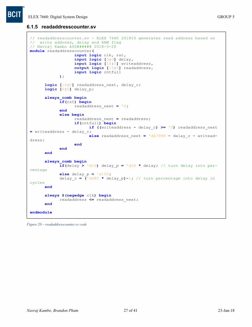
6.1.5 readaddresscounter.sv
Figure 20 – readaddresscounter.sv code
// readaddresscounter.sv - ELEX 7660 201810 generates read address based on
// write address, delay and RAM flag
// Navraj Kambo A00###### 2018-3-20
module readaddresscounter(
input logic clk, rst,
input logic [3:0] delay,
input logic [15:0] writeaddress,
output logic [15:0] readaddress,
input logic cntfull
);
logic [15:0] readaddress_next, delay_c;
logic [6:0] delay_p;
always_comb begin
if(rst) begin
readaddress_next = '0;
end
else begin
readaddress_next = readaddress;
if(cntfull) begin
if ((writeaddress - delay_c) >= '0) readaddress_next
= writeaddress - delay_c;
else readaddress_next = 'd47999 - delay_c - writead-
dress;
end
end
end
always_comb begin
if(delay > 'd10) delay_p = 'd10 * delay; // turn delay into per-
centage
else delay_p = 'd100;
delay_c = ('d480 * delay_p)-1; // turn percentage into delay in
cycles
end
always @(negedge clk) begin
readaddress <= readaddress_next;
end
endmodule

ELEX 7660: Digital System Design GROUP 5
Navraj Kambo, Brandon Pham 28 of 41 23-Jan-18
6.1.6 writeaddresscounter.sv
Figure 21 – writeaddresscounter.sv code
// writeaddresscounter.sv - ELEX 7660 201810 generates write address and
// and counts up to 48000 before resetting
// Navraj Kambo A00###### 2018-3-19
module writeaddresscounter(
input logic clk, rst,
input logic ivalid,
output logic cntfull,
output logic [15:0] writeaddress
);
logic [15:0] writeaddress_next;
logic cntfull_next;
always_comb begin
if(rst) begin
writeaddress_next = '0;
cntfull_next = '0;
end
else begin
writeaddress_next = writeaddress;
cntfull_next = cntfull;
if(writeaddress >= 'd47999)begin writeaddress_next = '0;
cntfull_next = '1; end
else writeaddress_next += 1;
end
end
always @(posedge rst or negedge ivalid) begin
writeaddress <= writeaddress_next;
cntfull <= cntfull_next;
end
endmodule

ELEX 7660: Digital System Design GROUP 5
Navraj Kambo, Brandon Pham 29 of 41 23-Jan-18
Figure 22 – write_tb.sv code
// write_tb.sv - ELEX 7660 201810 read and write address counter testbench
// Navraj Kambo A00###### 2018-3-22
module write_tb();
writeaddresscounter wcnt(.*);
readaddresscounter rcnt(.*);
logic clk, clk_48k, clk_50m, rst;
logic [3:0] delay = 'd1;
logic ivalid, cntfull;
logic [15:0] writeaddress, readaddress;
logic [16:0] i;
assign clk = clk_50m;
initial begin
rst = '0;
// generate reset signal
#20ns rst = '1;
#40ns begin rst = '0; end
end
initial begin
clk_50m = '1;
forever begin
#10ns clk_50m = ~clk_50m;
end
end
initial begin
clk_48k = '1;
forever begin
#10.4166us clk_48k = ~clk_48k;
end
end
initial begin
@(negedge rst) begin
for (i=0; i<65538; i=i+1) begin
ivalid = '1;
#10.4166us ivalid = '0;
#10.4166us ;
end
$stop;
end
end
endmodule

ELEX 7660: Digital System Design GROUP 5
Navraj Kambo, Brandon Pham 30 of 41 23-Jan-18
6.1.7 sevensegdecoder.sv
Figure 23 – sevensegdecoder.sv code
// sevensegdecoder.sv - ELEX 7660 201810 decoder for seven segment displays
// Navraj Kambo A00###### 2018-3-19
module sevensegdecorder(
input logic [3:0] din,
output logic [6:0] dout
);
always_comb begin
unique case(din)
'd0: dout = 7'b1000000;
'd1: dout = 7'b1111001;
'd2: dout = 7'b0100100;
'd3: dout = 7'b0110000;
'd4: dout = 7'b0011001;
'd5: dout = 7'b0010010;
'd6: dout = 7'b0000010;
'd7: dout = 7'b1111000;
'd8: dout = 7'b0000000;
'd9: dout = 7'b0010000;
'd10: dout = 7'b0001000;
'd11: dout = 7'b0000011;
'd12: dout = 7'b1000110;
'd13: dout = 7'b0100001;
'd14: dout = 7'b0000110;
'd15: dout = 7'b0001110;
default: dout = 7'b1000000;
endcase
end
endmodule

ELEX 7660: Digital System Design GROUP 5
Navraj Kambo, Brandon Pham 31 of 41 23-Jan-18
6.1.8 delayoutput.sv
Figure 24 – delayoutput.sv code(1)
// delayoutput.sv - ELEX 7660 201810 displays delay in ms on 7 segment
// displays
// Navraj Kambo A00###### 2018-3-25
module delayoutput(
input clk, rst,
input logic [3:0] delay,
output logic [6:0] HEX0,
output logic [6:0] HEX1,
output logic [6:0] HEX2,
output logic [6:0] HEX3
);
sevensegdecorder displ0(
.din(dispnum0),
.dout(HEX0)
);
sevensegdecorder displ1(
.din(dispnum1),
.dout(HEX1)
);
sevensegdecorder displ2(
.din(dispnum2),
.dout(HEX2)
);
sevensegdecorder displ3(
.din(dispnum3),
.dout(HEX3)
);
logic [3:0] dispnum0,dispnum1,dispnum2,dispnum3;
logic [3:0] dispnum0_next,dispnum1_next,dispnum2_next,dispnum3_next;
always_comb begin
if(rst) begin
dispnum0_next = 'd0;
dispnum1_next = 'd0;
dispnum2_next = 'd0;
dispnum3_next = 'd0;
end
else begin
dispnum0_next = dispnum0;
dispnum1_next = dispnum1;
dispnum2_next = dispnum2;
dispnum3_next = dispnum3;
dispnum0_next = '0;
dispnum1_next = '0;
unique case(delay)
'd1: begin
dispnum2_next ='d1;
dispnum3_next ='d0;
end
'd2: begin
dispnum2_next ='d2;
dispnum3_next ='d0;
end
'd3: begin
dispnum2_next ='d3;

ELEX 7660: Digital System Design GROUP 5
Navraj Kambo, Brandon Pham 32 of 41 23-Jan-18
Figure 25 – delayoutput.sv code(2)
6.1.9 tencounter.sv
dispnum3_next ='d0; end 'd4: begin dispnum2_next ='d4; dispnum3_next ='d0; end 'd5: begin dispnum2_next ='d5; dispnum3_next ='d0; end 'd6: begin dispnum2_next ='d6; dispnum3_next ='d0; end 'd7: begin dispnum2_next ='d7; dispnum3_next ='d0; end 'd8: begin dispnum2_next ='d8; dispnum3_next ='d0; end 'd9: begin dispnum2_next ='d9; dispnum3_next ='d0; end 'd10: begin dispnum2_next ='d0; dispnum3_next ='d1; end default: begin dispnum2_next ='d0; dispnum3_next ='d0; end endcase end end
always @(posedge clk) begin dispnum0 = dispnum0_next; dispnum1 = dispnum1_next; dispnum2 = dispnum2_next; dispnum3 = dispnum3_next; end endmodule

ELEX 7660: Digital System Design GROUP 5
Navraj Kambo, Brandon Pham 33 of 41 23-Jan-18
6.1.10 sinewave.sv
Figure 27 – sinewave.sv code(1)
// sinewave.sv - ELEX 7660 201810 sinewave LUT
// Navraj Kambo A00###### 2018-4-6
module sinewave(
input logic clk, rst,
input logic [6:0] count,
output logic [7:0] data_out
);
logic [99:0][7:0]sine;
initial begin
sine[0] = 'd0;
sine[1] = 'd0;
sine[2] ='d1;
sine[3] ='d1;
sine[4] ='d1;
sine[5] ='d1;
sine[6] ='d2;
sine[7] ='d2;
sine[8] ='d2;
sine[9] ='d2;
sine[10] ='d3;
sine[11] ='d3;
sine[12] ='d3;
sine[13] ='d3;
sine[14] ='d3;
sine[15] ='d4;
sine[16] ='d4;
sine[17] ='d4;
sine[18] ='d4;
sine[19] ='d5;
sine[20] ='d5;
sine[21] ='d5;
sine[22] ='d5;
sine[23] ='d6;
sine[24] ='d6;
sine[25] ='d6;
sine[26] ='d6;
sine[27] ='d7;
sine[28] ='d7;
sine[29] ='d7;
sine[30] ='d7;
sine[31] ='d7;
sine[32] ='d8;
sine[33] ='d8;
sine[34] ='d8;
sine[35] ='d8;
sine[36] ='d9;
sine[37] ='d9;
sine[38] ='d9;
sine[39] ='d9;
sine[40] ='d9;
sine[41] ='d10;
sine[42] ='d10;
sine[43] ='d10;
sine[44] ='d10;
sine[45] ='d10;
sine[46] ='d11;
sine[47] ='d11;

ELEX 7660: Digital System Design GROUP 5
Navraj Kambo, Brandon Pham 34 of 41 23-Jan-18
Figure 28 – sinewave.sv code(2)
sine[48] ='d11; sine[49] ='d11; sine[50] ='d11; sine[51] ='d11; sine[52] ='d12; sine[53] ='d12; sine[54] ='d12; sine[55] ='d12; sine[56] ='d12; sine[57] ='d12; sine[58] ='d13; sine[59] ='d13; sine[60] ='d13; sine[61] ='d13; sine[62] ='d13; sine[63] ='d13; sine[64] ='d14; sine[65] ='d14; sine[66] ='d14; sine[67] ='d14; sine[68] ='d14; sine[69] ='d14; sine[70] ='d14; sine[71] ='d14; sine[72] ='d14; sine[73] ='d15; sine[74] ='d15; sine[75] ='d15; sine[76] ='d15; sine[77] ='d15; sine[78] ='d15; sine[79] ='d15; sine[80] ='d15; sine[81] ='d15; sine[82] ='d15; sine[83] ='d15; sine[84] ='d15; sine[85] ='d16; sine[86] ='d16; sine[87] ='d16; sine[88] ='d16; sine[89] ='d16; sine[90] ='d16; sine[91] ='d16; sine[92] ='d16; sine[93] ='d16; sine[94] ='d16; sine[95] ='d16; sine[96] ='d16; sine[97] ='d16; sine[98] ='d16; sine[99] ='d16; end always_comb begin data_out = sine[count]; end endmodule
ELEX 7660: Digital System Design GROUP 5
Navraj Kambo, Brandon Pham 35 of 41 23-Jan-18
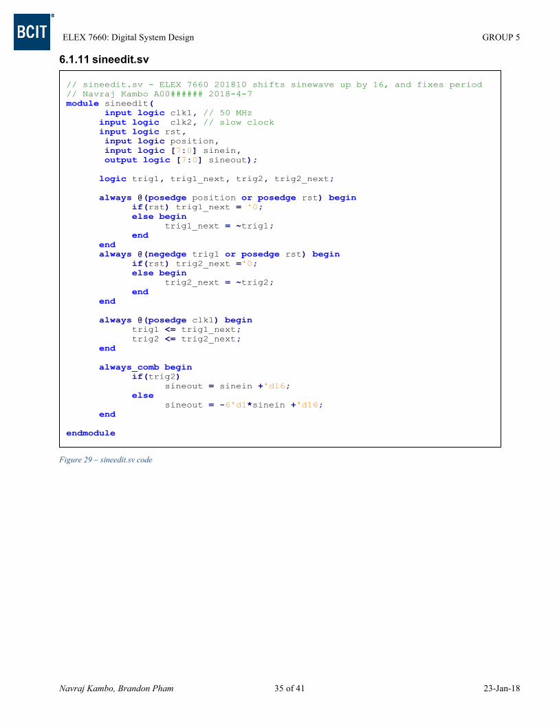
6.1.11 sineedit.sv
Figure 29 – sineedit.sv code
// sineedit.sv - ELEX 7660 201810 shifts sinewave up by 16, and fixes period
// Navraj Kambo A00###### 2018-4-7
module sineedit(
input logic clk1, // 50 MHz
input logic clk2, // slow clock
input logic rst,
input logic position,
input logic [7:0] sinein,
output logic [7:0] sineout);
logic trig1, trig1_next, trig2, trig2_next;
always @(posedge position or posedge rst) begin
if(rst) trig1_next = '0;
else begin
trig1_next = ~trig1;
end
end
always @(negedge trig1 or posedge rst) begin
if(rst) trig2_next ='0;
else begin
trig2_next = ~trig2;
end
end
always @(posedge clk1) begin
trig1 <= trig1_next;
trig2 <= trig2_next;
end
always_comb begin
if(trig2)
sineout = sinein +'d16;
else
sineout = -6'd1*sinein +'d16;
end
endmodule

ELEX 7660: Digital System Design GROUP 5
Navraj Kambo, Brandon Pham 36 of 41 23-Jan-18
Figure 30 – tencounter_tb.sv code
// tencounter_tb.sv - ELEX 7660 201810 sinewave testbench
// Navraj Kambo A00###### 2018-4-7
`timescale 1ns / 1ns
module tencounter_tb();
logic clk_50m, clk, rst;
logic clk_out;
logic [6:0] count;
logic position, position_next;
logic flg, flg_next;
logic [7:0] sinewavex, sinewaveo;
assign clk = clk_50m;
// instantiation
tencounter cntten(.*);
hundredudcounter cnthun(.clk(clk_out), .rst(rst), .count(count), .posi-
tion(position_next));
sinewave sinfunc(
.clk(clk),
.rst(rst),
.count(count),
.data_out(sinewavex)
);
sineedit sinefun2(
.clk1(clk),
.clk2(clk_out),
.rst(rst),
.position(position),
.sinein(sinewavex),
.sineout(sinewaveo)
);
// start tb code
initial begin
rst = '0;
// generate reset signal
#20ns rst = '1;
#40ns begin rst = '0; end
end
initial begin
clk_50m = '1;
forever begin
#10ns clk_50m = ~clk_50m;
end
end
always @(posedge clk_out) begin
if(rst) begin
flg_next = '0;
end
else begin
flg_next = flg;
if(count == 'd99) begin
flg_next = '1;
end
if(flg && count == '0) flg_next = '0;
end
end
always_comb begin
$display("%b", position);
end

ELEX 7660: Digital System Design GROUP 5
Navraj Kambo, Brandon Pham 37 of 41 23-Jan-18
6.2 Audio Hardware Processor Schematic
Figure 31 - Top level schematic audio hardware processor without effects

ELEX 7660: Digital System Design GROUP 5
Navraj Kambo, Brandon Pham 38 of 41 23-Jan-18
6.3 Effect Controller Code 6.3.1 effectcontrol.sv (top-level)
Figure 32 - effectcontrol.sv code(1) (top-level)
// effectcontrol.sv - ELEX 7660 201810 top level entity of effect controller
// module (DE0-Nano)
// Brandon Pham A00###### 2018-3-10
module effectcontrol (output logic [3:0] count,
output logic [7:0] LED,
output logic volup, voldown,
input logic volupin, voldownin, CLOCK_50);
logic [3:0] count_next;
logic countup, countdown;
logic clk;
pll pll0 ( .inclk0(CLOCK_50), .c0(clk) ) ;
always_comb begin
count_next = count;
if(volupin) begin
if (count < 10)
count_next = count_next + 1;
else
count_next = count_next;
end
if(voldownin) begin
if (count > 0)
count_next = count_next - 1;
else
count_next = count_next;
end
unique case (count)
0: LED = 8'b0000_0000;
1: LED = 8'b0000_0001;
2: LED = 8'b0000_0011;
3: LED = 8'b0000_0111;
4: LED = 8'b0000_1111;
5: LED = 8'b0001_1111;
6: LED = 8'b0011_1111;
7: LED = 8'b0111_1111;
8: LED = 8'b1111_1111;
9: LED = 8'b1111_1110;
10: LED = 8'b1111_1100;
default: LED = 8'b0101_0101;
endcase
end
always_ff @(posedge clk) begin
count <= count_next;
end
endmodule
// megafunction wizard: %ALTPLL%
// ...
// THIS IS A WIZARD-GENERATED FILE. DO NOT EDIT THIS FILE!
// ...
module pll ( inclk0, c0);
input inclk0;
output c0;
wire [0:0] sub_wire2 = 1'h0;
wire [4:0] sub_wire3;
wire sub_wire0 = inclk0;

ELEX 7660: Digital System Design GROUP 5
Navraj Kambo, Brandon Pham 39 of 41 23-Jan-18
Figure 33 - effectcontrol.sv code(2) (top-level)
wire [1:0] sub_wire1 = {sub_wire2, sub_wire0}; wire [0:0] sub_wire4 = sub_wire3[0:0]; wire c0 = sub_wire4; altpll altpll_component ( .inclk (sub_wire1), .clk (sub_wire3), .activeclock (), .areset (1'b0), .clkbad (), .clkena ({6{1'b1}}), .clkloss (), .clkswitch (1'b0), .configupdate (1'b0), .enable0 (), .enable1 (), .extclk (), .extclkena ({4{1'b1}}), .fbin (1'b1), .fbmimicbidir (), .fbout (), .fref (), .icdrclk (), .locked (), .pfdena (1'b1), .phasecounterselect ({4{1'b1}}), .phasedone (), .phasestep (1'b1), .phaseupdown (1'b1), .pllena (1'b1), .scanaclr (1'b0), .scanclk (1'b0), .scanclkena (1'b1), .scandata (1'b0), .scandataout (), .scandone (), .scanread (1'b0), .scanwrite (1'b0), .sclkout0 (), .sclkout1 (), .vcooverrange (), .vcounderrange ()); defparam altpll_component.bandwidth_type = "AUTO", altpll_component.clk0_divide_by = 10000, altpll_component.clk0_duty_cycle = 50, altpll_component.clk0_multiply_by = 1, altpll_component.clk0_phase_shift = "0", altpll_component.compensate_clock = "CLK0", altpll_component.inclk0_input_frequency = 20000, altpll_component.intended_device_family = "Cyclone IV E", altpll_component.lpm_hint = "CBX_MODULE_PREFIX=lab1clk", altpll_component.lpm_type = "altpll", altpll_component.operation_mode = "NORMAL", altpll_component.pll_type = "AUTO", altpll_component.port_activeclock = "PORT_UNUSED", altpll_component.port_areset = "PORT_UNUSED", altpll_component.port_clkbad0 = "PORT_UNUSED", altpll_component.port_clkbad1 = "PORT_UNUSED", altpll_component.port_clkloss = "PORT_UNUSED", altpll_component.port_clkswitch = "PORT_UNUSED", altpll_component.port_configupdate = "PORT_UNUSED", altpll_component.port_fbin = "PORT_UNUSED", altpll_component.port_inclk0 = "PORT_USED", altpll_component.port_inclk1 = "PORT_UNUSED", altpll_component.port_locked = "PORT_UNUSED", altpll_component.port_pfdena = "PORT_UNUSED", altpll_component.port_phasecounterselect = "PORT_UNUSED", altpll_component.port_phasedone = "PORT_UNUSED", altpll_component.port_phasestep = "PORT_UNUSED", altpll_component.port_phaseupdown = "PORT_UNUSED", altpll_component.port_pllena = "PORT_UNUSED", altpll_component.port_scanaclr = "PORT_UNUSED", altpll_component.port_scanclk = "PORT_UNUSED", altpll_component.port_scanclkena = "PORT_UNUSED", altpll_component.port_scandata = "PORT_UNUSED", altpll_component.port_scandataout = "PORT_UNUSED", altpll_component.port_scandone = "PORT_UNUSED", altpll_component.port_scanread = "PORT_UNUSED", altpll_component.port_scanwrite = "PORT_UNUSED", altpll_component.port_clk0 = "PORT_USED", altpll_component.port_clk1 = "PORT_UNUSED", altpll_component.port_clk2 = "PORT_UNUSED",

ELEX 7660: Digital System Design GROUP 5
Navraj Kambo, Brandon Pham 40 of 41 23-Jan-18
Figure 34 - effectcontrol.sv code(3) (top-level)
6.4 Effect Controller Schematic
Figure 35 - Effect controller schematic
altpll_component.port_clk3 = "PORT_UNUSED", altpll_component.port_clk4 = "PORT_UNUSED", altpll_component.port_clk5 = "PORT_UNUSED", altpll_component.port_clkena0 = "PORT_UNUSED", altpll_component.port_clkena1 = "PORT_UNUSED", altpll_component.port_clkena2 = "PORT_UNUSED", altpll_component.port_clkena3 = "PORT_UNUSED", altpll_component.port_clkena4 = "PORT_UNUSED", altpll_component.port_clkena5 = "PORT_UNUSED", altpll_component.port_extclk0 = "PORT_UNUSED", altpll_component.port_extclk1 = "PORT_UNUSED", altpll_component.port_extclk2 = "PORT_UNUSED", altpll_component.port_extclk3 = "PORT_UNUSED", altpll_component.width_clock = 5; endmodule

ELEX 7660: Digital System Design GROUP 5
Navraj Kambo, Brandon Pham 41 of 41 23-Jan-18
6.5 MATLAB Code
Figure 36 - matlabfx.m code
// Navraj Kambo A00###### 2018-3-10
function y=convreverb(x, h)
ly=length(x)+length(h)-1;
ly2=pow2(nextpow2(ly));
X = fft(x, ly2);
H = fft(h, ly2);
Y = X.*H;
y = real(ifft(Y,ly2));
y = y(1:1:ly);
y=y/max(abs(y));
end
function y=flanger(x,Fs,max_time_delay,rate)
% parameters to vary the effect %
%max_time_delay=0.003; % 3ms max delay in seconds
%rate=1; %rate of flange in Hz
index=1:length(x);
% sin reference to create oscillating delay
sin_ref = (sin(2*pi*index*(rate/Fs)));
%convert delay in ms to max delay in samples
max_samp_delay=round(max_time_delay*Fs);
% create empty out vector
y = zeros(length(x),1);
% to avoid referencing of negative samples
y(1:max_samp_delay)=x(1:max_samp_delay);
% set amp suggested coefficient from page 71 DAFX
amp=0.7;
% for each sample
for i = (max_samp_delay+1):length(x)
cur_sin=abs(sin_ref(i)); %abs of current sin val 0-1
% generate delay from 1-max_samp_delay and ensure whole number
cur_delay=ceil(cur_sin*max_samp_delay);
% add delayed sample
y(i) = (amp*x(i)) + amp*(x(i-cur_delay));
end
end
function y=simpecho(x, Fs, D, R, a)
length = size(x); % get the length of the music file
D = round(D*Fs); % set the delay time in samples
y = zeros(length); % initialize the output music signal
for i = (R*D) + 1 : 1 : length
y(i) = x(i);
for n=1:1:R
y(i) = y(i) + (a/n)*x(i-(n*D));
end
end
end
function y=tremolo(x,Fs,Fc,alpha)
index = 1:length(x);
sin_ref = sin(2*pi*index*(Fc/Fs));
y = x;
for i=1:length(x)
trem = 1 + alpha*sin_ref(i);
y(i) = trem*x(i);
end
end