Embed Size (px)
Citation preview

Semiconductor
Memories
Jan M. Rabaey
Anantha Chandrakasan
Borivoje Nikolic
Paolo Spirito

Elena Gnani
Memory Classification

Elena Gnani
Memory Classification
Non-Random
Access
Read-Write MemoryNon-Volatile
Read-Write
Memory
Read-Only Memory
EPROM
E2PROM
FLASH
Random
Access
SRAM
DRAM
Mask-Programmed
Programmable (PROM)
FIFO
Shift Register
CAM
LIFO

Elena Gnani
Memory Classification

Elena Gnani
Memory access time
Elena Gnani
Memory timing: definitions

Elena Gnani
Elena Gnani
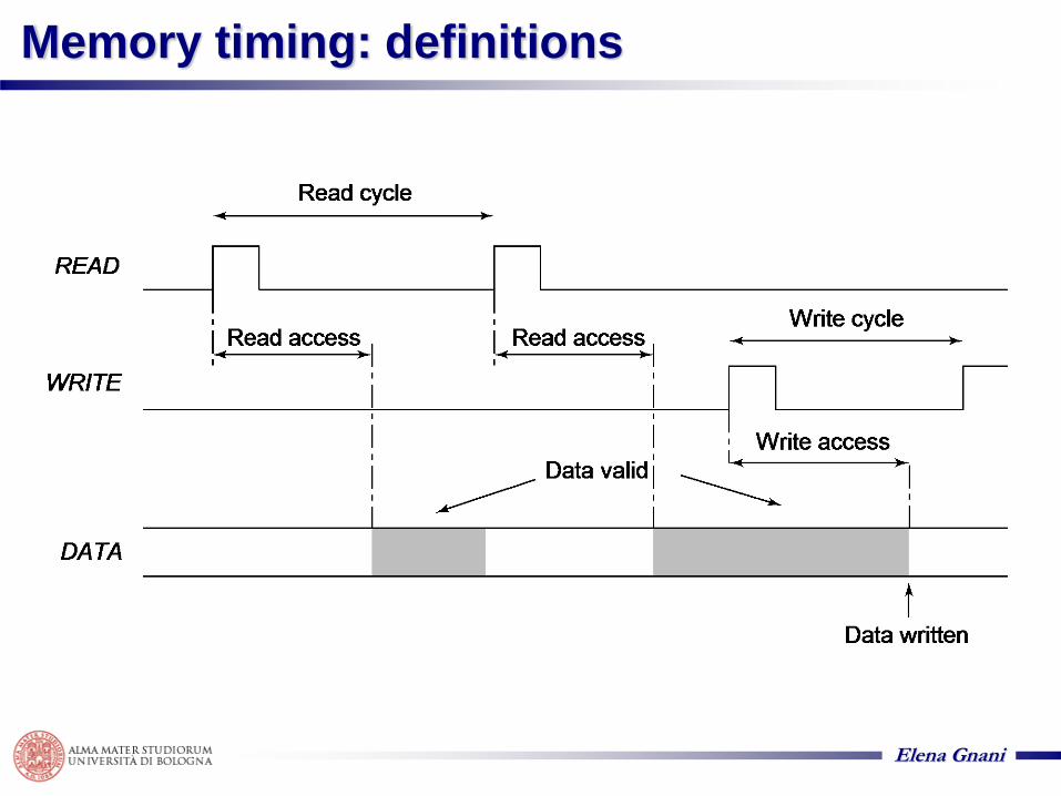
RAM memory Architecture
Storage
cell
Storage
cell
Input-Output
M bits
Intuitive architecture for N x M memory
Too many select signals:
N words => N select signalsK = log2N
Decoder reduces the number of select signals
Input-Output
M bits
M bits
Word 0
Word 1
Word 2
Word N – 2
Word N – 1
M bits
SN-1
S0
S1
K = log2 N
Word 2
AK−1
A1
A0
S0
SN – 1
Word 0
Word 1
Word N – 2
Word N – 1
Elena Gnani
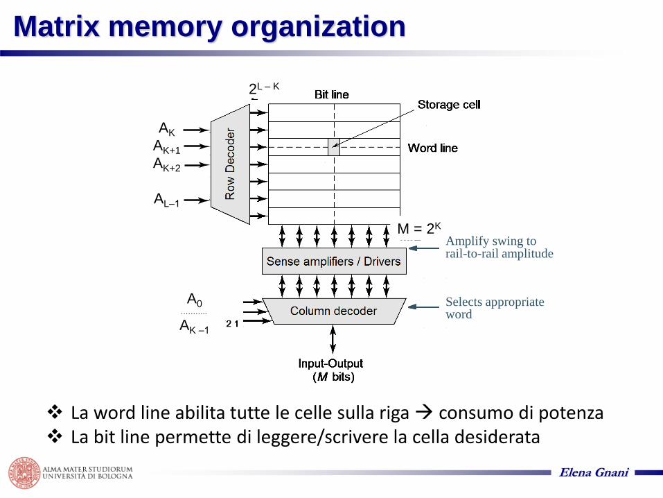
Matrix memory organization
Elena Gnani
Matrix memory organization
Amplify swing torail-to-rail amplitude
Selects appropriateword
A
A
A
A
A
AK
AK+1
AK+2
AL‒1
2L ‒ K
A0………..
AK ‒1
M = 2K
La word line abilita tutte le celle sulla riga consumo di potenza La bit line permette di leggere/scrivere la cella desiderata

Elena Gnani
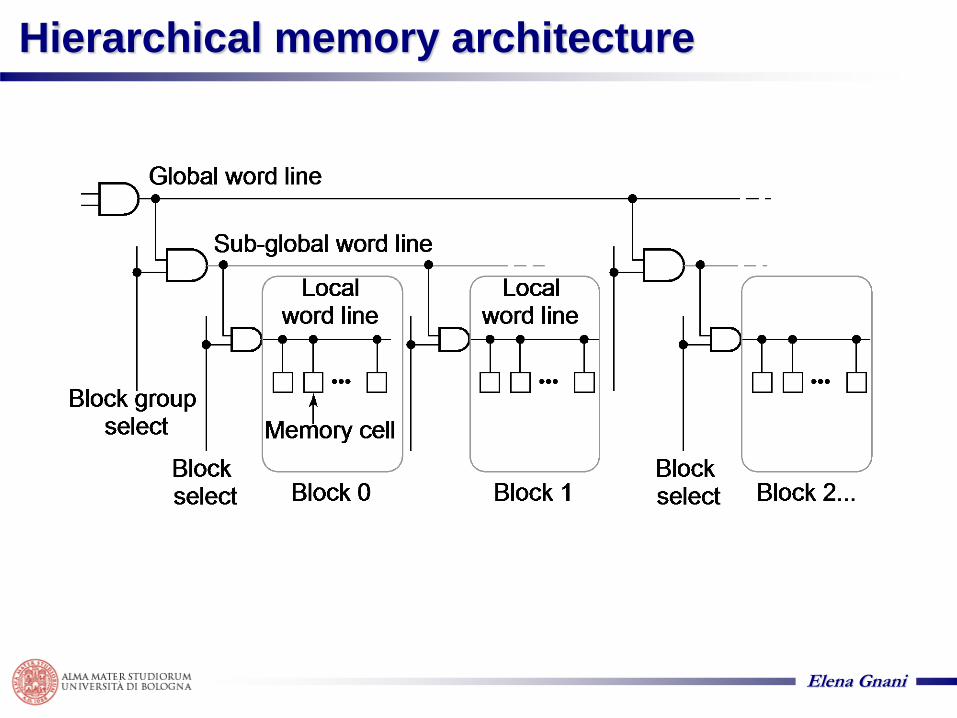
Hierarchical memory architecture
Advantages:
1. Shorter wires within blocks
2. Block address activates only 1 block => power savings
P −1
Elena Gnani
Hierarchical memory architecture
Elena Gnani
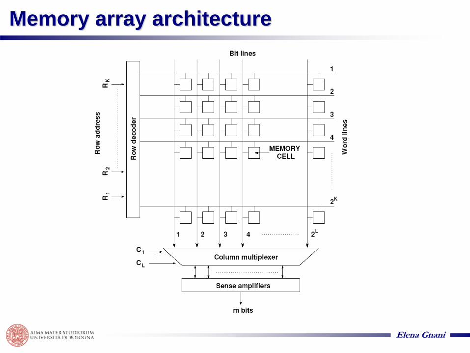
Memory array architecture

Elena Gnani
Power dissipation in memories

Elena Gnani
Elena Gnani
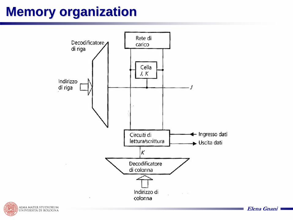
Memory organization

Elena Gnani
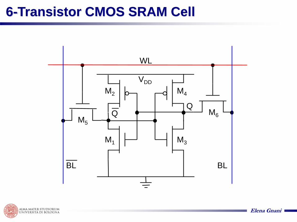
6-Transistor CMOS SRAM Cell
Elena Gnani
6-Transistor CMOS SRAM Cell
VDD
M5
M6
M4
M1
M2
M3
WL
BLBL
Elena Gnani
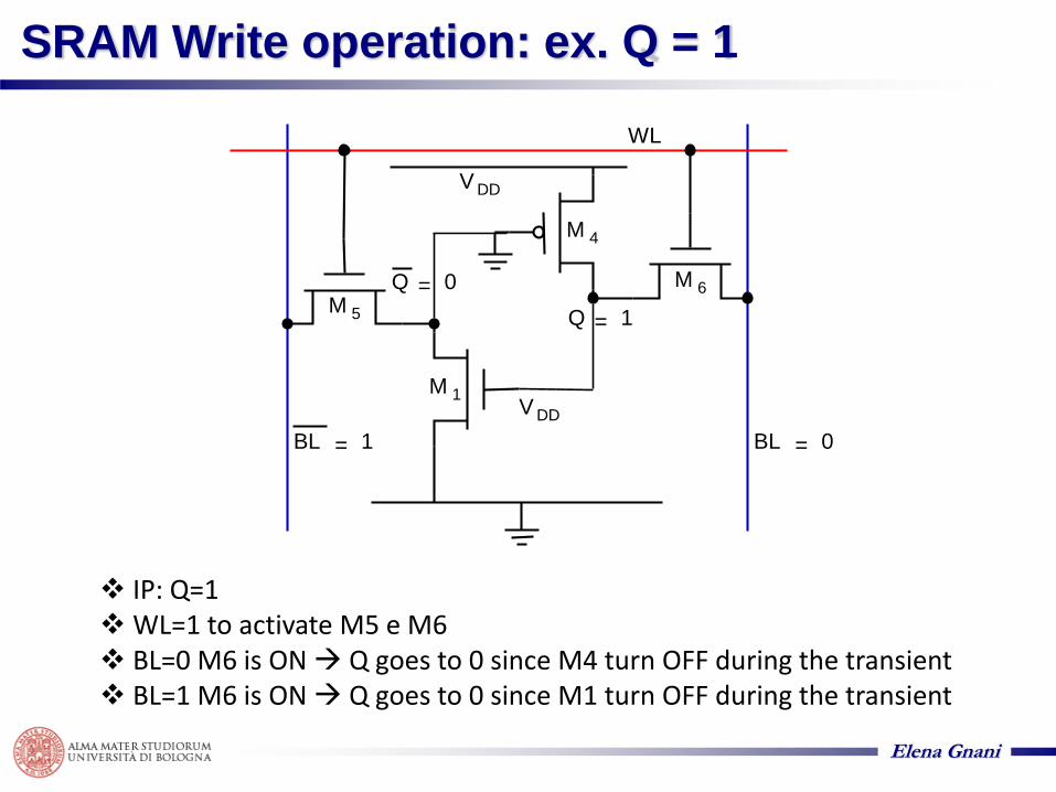
SRAM Write operation: ex. Q = 1
IP: Q=1 WL=1 to activate M5 e M6 BL=0 M6 is ON Q goes to 0 since M4 turn OFF during the transient BL=1 M6 is ON Q goes to 0 since M1 turn OFF during the transient
BL = 1 BL = 0
Q = 0
Q = 1
M 1
M 4
M 5
M 6
V DD
V DD
WL

Elena Gnani
SRAM Write operation

Elena Gnani
SRAM Read operation: ex. Q = 1
WL
BL
VDD
M 5
M 6
M 4
M 1V DDV DD V DD
BL
Q = 1Q = 0
Cbit Cbit

Elena Gnani
Resistive-load SRAM cell
Static power dissipation: want RL large
Bit lines precharged to VDD to address tp problem
M3
RL RL
VDD
WL
Q Q
M1 M2
M4
BL BL
Elena Gnani
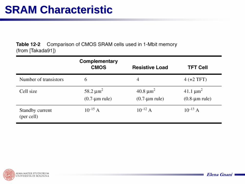
SRAM Characteristic

Elena Gnani
Sense amplifiers
outputinput
s.a.smalltransition
Il sense amplifier è un circuito in grado di amplificare le variazioni
presenti sul segnale di ingresso un piccolo sbilanciamento delle
tensioni su BL e BL’ viene amplificato.
Elena Gnani
Memory Classification
Amplify swing torail-to-rail amplitude
Selects appropriateword
A
A
A
A
A
AK
AK+1
AK+2
AL‒1
2L ‒ K
A0………..
AK ‒1
M = 2K
Elena Gnani
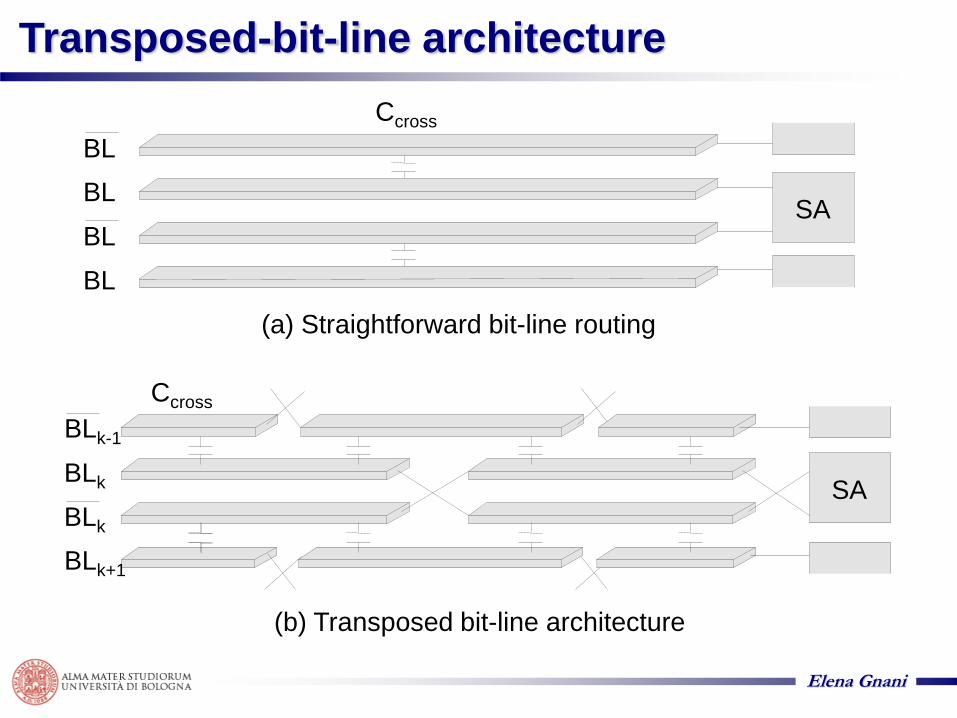
Transposed-bit-line architecture
SA
Ccross
(a) Straightforward bit-line routing
(b) Transposed bit-line architecture
BL
BL
BL
BL
SA
Ccross
BLk-1
BLk
BLk
BLk+1
Elena Gnani
Elena Gnani
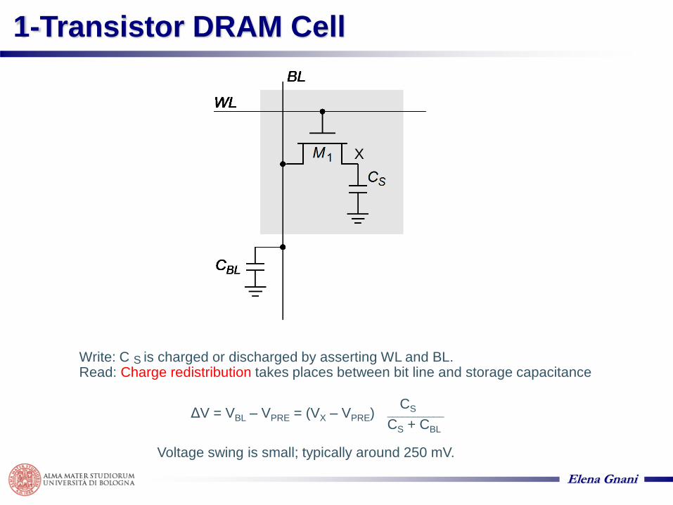
1-Transistor DRAM Cell
Write: C S is charged or discharged by asserting WL and BL.Read: Charge redistribution takes places between bit line and storage capacitance
Voltage swing is small; typically around 250 mV.
ΔV = VBL – VPRE = (VX – VPRE) ___________
CS + CBL
CS
X

Elena Gnani
Read operation

Elena Gnani
Write operation
Avrò in transitorio la cui durata dipende dalla resistività di M1
Elena Gnani
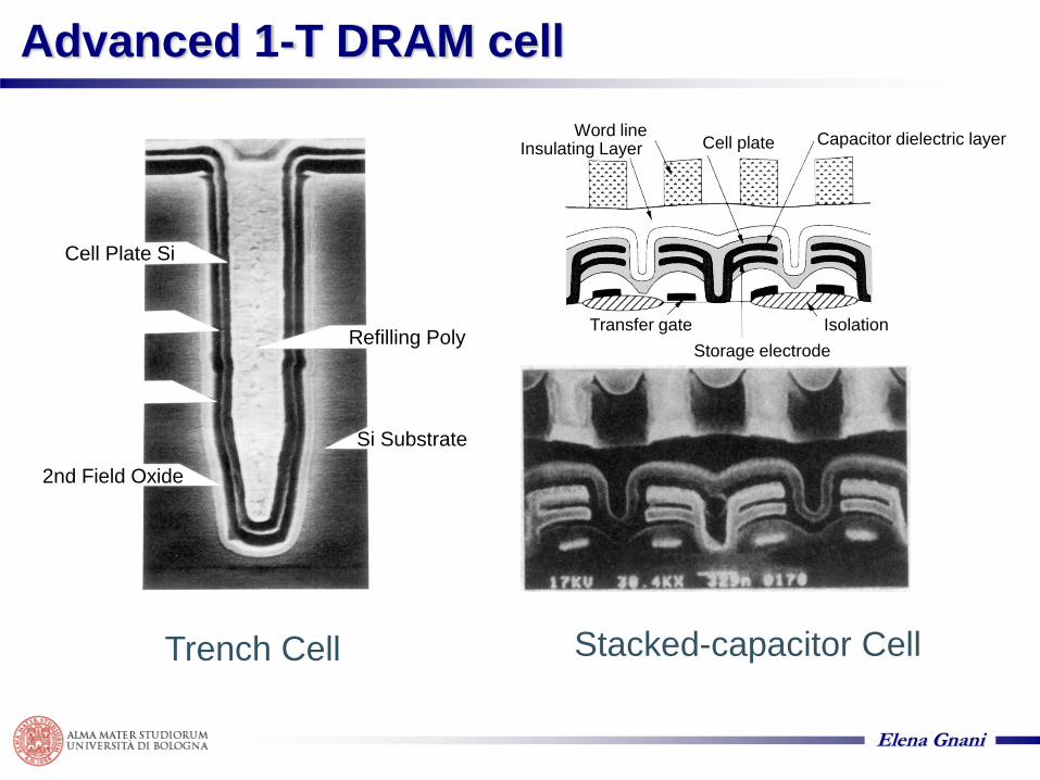
Advanced 1-T DRAM cell
Cell Plate Si
2nd Field Oxide
Refilling Poly
Si Substrate
Trench Cell Stacked-capacitor Cell
Capacitor dielectric layerCell plateWord line
Insulating Layer
IsolationTransfer gate
Storage electrode

Elena Gnani
Future DRAM Technology
Elena Gnani
1-Transistor DRAM Cell
1T DRAM requires a sense amplifier for each bit line, due to charge redistribution read-out.
DRAM memory cells are single ended in contrast to SRAM cells.
The read-out of the 1T DRAM cell is destructive refresh is necessary for correct operation.
The 1T cell requires presence of a capacitance that must be explicitly included in the design.
When writing a “1” into a DRAM cell, a threshold voltage is lost (M1 in pass transistor configuration) this loss can be circumvented by boot-strapping the word lines to a value higher than VDD

Elena Gnani
Noise sources in 1-T DRAM
Ccross
electrode
leakageCS
WL
BL substrate Adjacent BL
CWBL
Elena Gnani
Read-Write RAM
Elena Gnani
Perifery
Decoders
Sense Amplifiers
Input/Output Buffers
Control & Timing Circuitry
Elena Gnani
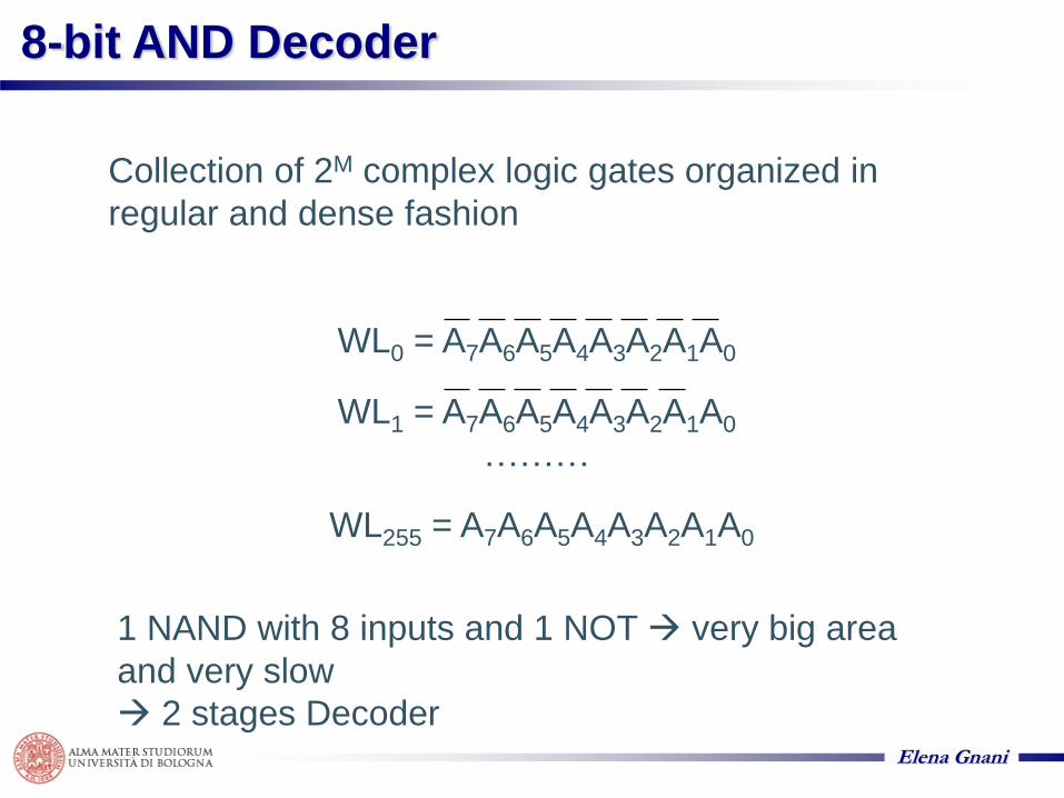
8-bit AND Decoder
Collection of 2M complex logic gates organized in
regular and dense fashion
WL0 = A7A6A5A4A3A2A1A0
WL1 = A7A6A5A4A3A2A1A0
………
WL255 = A7A6A5A4A3A2A1A0
1 NAND with 8 inputs and 1 NOT very big area
and very slow
2 stages Decoder

Elena Gnani
10-bit NOR Decoder
WL0 = A7+A6+A5+A4+A3+A2+A1+A0
WL1 = A7+A6+A5+A4+A3+A2+A1+A0
…………
…………
…………
WL255 = A7+A6+A5+A4+A3+A2+A1+A0
1 NOR with 8 inputs (16 T) 1 stage Decoder
Number T: 256 x 16 = 4096 T

Elena Gnani
Hierarchical decoders
WL0 = A7A6A5A4A3A2A1A0
WL0 = A7A6A5A4A3A2A1A0
WL0 = (A7+A6)(A5+A4)(A3+A2)(A1+A0)
The address is partitioned into sections of 2 bits that
are decoded in advance. The resulting signal are then
combined using 4-input NAND gates
1 4-input NAND
4 2-input NOR

Elena Gnani
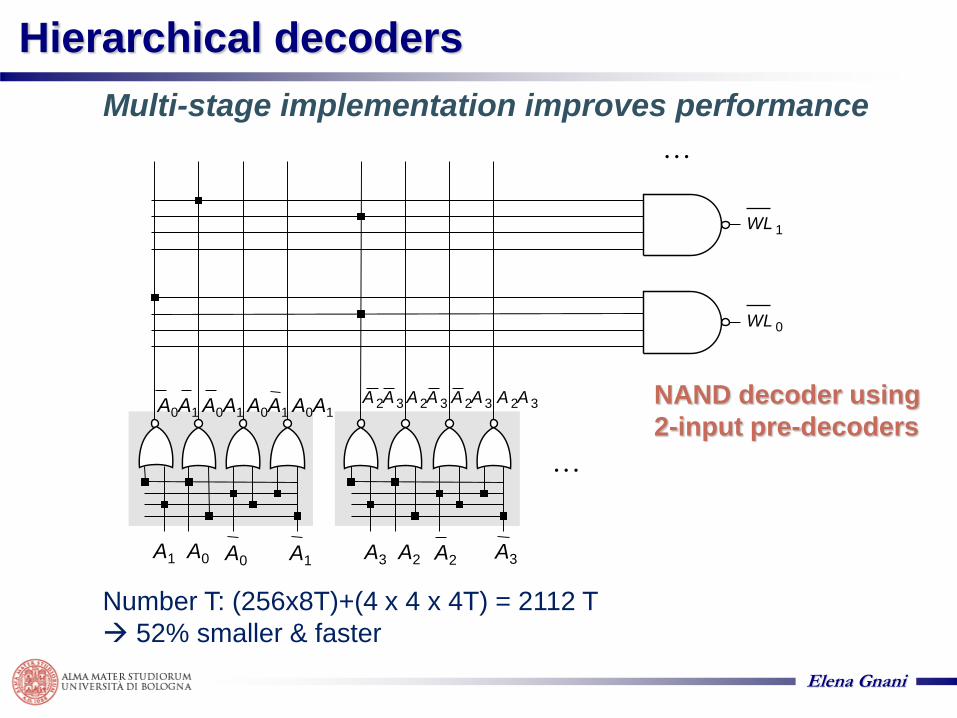
Hierarchical decoders
• • •
• • •
A2
A 2A3
WL 0
A2A3A2A 3A2A3
A3 A2 A3
WL 1
Multi-stage implementation improves performance
NAND decoder using
2-input pre-decoders
A0A1 A0 A1
A0A1 A0A1 A0A1 A0A1
Number T: (256x8T)+(4 x 4 x 4T) = 2112 T
52% smaller & faster
Elena Gnani
Hierarchical decoders
• • •
• • •
A2
A 2A3
WL 0
A2A3A2A 3A2A3
A3 A2 A3
WL 1
Multi-stage implementation improves performance
NAND decoder using
2-input pre-decoders
A0A1 A0 A1
A0A1 A0A1 A0A1 A0A1
Number T: (256x8T)+(4 x 4 x 4T) = 2112 T
52% smaller & faster
Elena Gnani
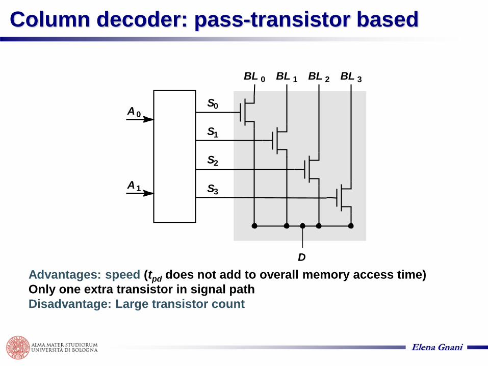
Column decoder: pass-transistor based
Advantages: speed (tpd does not add to overall memory access time)
Only one extra transistor in signal path
Disadvantage: Large transistor count
A0
S0
BL 0 BL 1 BL 2 BL 3
A1
S1
S2
S3
D
Elena Gnani
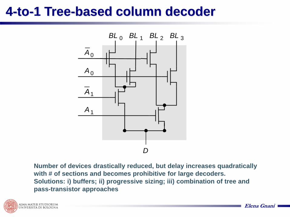
4-to-1 Tree-based column decoder
Number of devices drastically reduced, but delay increases quadratically
with # of sections and becomes prohibitive for large decoders.
Solutions: i) buffers; ii) progressive sizing; iii) combination of tree and
pass-transistor approaches
BL 0 BL 1 BL 2 BL 3
D
A 0
A 0
A1
A 1