Embed Size (px)
Citation preview

Electronics and Communication Engineering
B.E. Courses Lecture Plan
Semester (January to May) 2018-2019

ECC02: Electronics I
Week Theory
Lecture
day
Topic (Including assignment/ test)
1st 1. Review of semiconductor physics
2. Mass action law, carrier concentrations
3. Graded and step graded semiconductor and calculation of barrier potential
2nd 4. Drift and diffusion current
5. p-n junction diode: ideal model, exponential model
6. Analysis of diode circuits
3rd 7. Review of diode as rectifier
8. Diode as clipper and clamper
9. Physical structure & modes of operation of BJT
4th 10. Class Test
11. BJT characteristics
12. Biasing scheme for BJT
5th 13. Calculation of operating point
14. Numerical Problems
15. Different types of current mirror
6th 16. The Ebers-Moll model for BJT
17. Transistor as an amplifier and switch
18. Various configuration such CE/CB/CC
MID TERM
7th 19. Low frequency transistor model
20. Small signal analysis
21. Estimation of voltage gain, input resistance, output resistance
8th 22. Numerical problems
23. JFET characteristics and working principle
24. Biasing scheme for JFET
9th 25. Small signal analysis
26. Numerical problems
27. Class Test
28. MOSFET operation (Enhancement mode and depletion mode)
29. Biasing scheme for MOSFET
10th 30. various configuration such CD/CS/CG
31. The CMOS digital logic inverter
32. Numerical problems
11th 33. High frequency model
34. Introduction of Thyristor, UJT, SCR

LIST OF EXPERIMENT
1. Study of electronic components- active & passive, Electronic Instruments: CRO, Function
generator, Power Supply, Multi-meter, IC tester.
2. To study and plot V-I characteristics of Zener diode in reverse bias and p-n junction diode in
forward bias.
3. To study and perform half wave rectifier and bridge rectifier circuit. Plot the output waveform and
calculate efficiency.
4. To study and perform positive clipper, negative clipper and slicer circuit. Also draw output
waveform.
5. To study and perform positive clamper and negative clamper circuit. Also draw output waveform.
6. To study and perform R-C circuit as an Integrator & Differentiator.
7. To study and perform operation of transistor as a switch and to find out region of operation.
8. To plot output V-I characteristics of CE configuration for BJT.
Prof. Maneesha Gupta
Course Coordinator

ECC03: Digital Circuit and Systems
S. No. Topics to be covered No. of Lectures
1. Number System: Conversion from one base to another,
complements
02
2. Binary codes (BCD, 2421, excess-3, 84-2-1, gray) 01
3. Conversion form binary to gray and vice-versa, error correcting
code (parity addition, Hamming code)
02
4. Boolean Algebra: Axioms, Canonical & standard forms 02
5. Logic gates, Simplification of Boolean functions (up to 5
variables) using (i) K-map (ii) Tabulation (Quin-Mclusky)
method
03
6. NAND & NOR implementation 01
First Class Test
7. Combinational Logic: Design procedure, Adders, Subtractors 02
8. Code conversion, Binary parallel adder, Decimal adder 02
9. Magnitude comparator, Decoders, Encoders, Priority encoder 03
10. Multiplexer, Demultiplexer 02
11. ROM, PLA 02
Mid-Sem Examination
12. Sequential Logic: Flip-Flops, Analysis of sequential circuits 02
13. State reduction, State table, Excitation table 02
14. Design procedure, Registers, Shift registers 02
15. Ripple counter, Synchronous counter, Incorporate self correcting
conditions in counters
03
16. Timing Sequences (Ring counter & Johnson counter) 01
17. Logic Families: Characteristics, RTL, DTL, TTL (including tri-
state logic)
02
18. ECL, IIL, PMOS, NMOS, CMOS (Basic circuits of all families
with problems based on them), Comparison of families
02
19. Data convertors: DAC, ADC, V/F 02
Total lectures 38
Books to be referred
1. M M Mano, ``Digital logic and computer design ,’’ Prentica Hall India
2. Millman & Grabel, ``Microelectronics,’’ Tata McGraw Hill
3. Donald D. Givone, ``Digital principles & design,’’ Tata McGraw Hill
4. R. P. Jain, ``Modern digital electronics,’’ Tata McGraw Hill

List Of Experiments: ECC03
1. Verify the truth table of AND, OR, NOT, NAND, NOR, XOR and XNOR gates.
2. Implement all the above mentioned gates by using NAND and NOR gates only.
3. Design and implement half adder, full adder, half subtractor and full subtractor using
logic gates.
4. Design a 4 bit parallel adder using IC, further using the same IC implement BCD to
excess-3 code converter.
5. Design a 4 bit magnitude comparator using IC. Also implement 2 bit magnitude
comparator using gates only.
6. Design a 2 bit multiplier circuit that multiplies two numbers of 2 bit each and
implement it using 8x1 MUX.
7. Design and implement full adder circuit using decoder and gates. Also implement
the same by using complementary output decoder.
8. Design the following flip flops using NAND/NOR gates:-
i) S-R flip flop
ii) D flip flop
iii) J-K flip flop and
iv) T flip flop.
9. Design and implement mod-6 synchronous up counter using T flip flop.
10. Design a 2 bit Up/Down counter using J-K flip flop.

CEC03: Digital Logic Design
S.No. CONTENTS LECTURES
1 Number System: Conversion from one base to another, complements, Binary
codes (BCD, 2421, excess-3, 84-2-1, gray), conversion form binary to gray
and vice-versa, error correcting code (parity addition, Hamming code)
3
2 Boolean Algebra: Axioms, Canonical & standard forms, Logic gates,
Simplification of Boolean functions (up to 5 variables) using (i) K-map (ii)
Tabulation (Quin-Mclusky) method, NAND & NOR implementation
4
3 Combinational Logic: Design procedure, Adders, Subs tractors, Code
conversion, Binary parallel adder, Decimal adder, Magnitude comparator,
Decoders, Encoders, Priority encoder, Multiplexer, Demultiplexer, ROM,
PLA.
7
4 Sequential Logic: Flip-Flops, Analysis of sequential circuits, State reduction,
State table, Excitation table, Design procedure, Registers, Shift registers,
Ripple counter, Synchronous counter, Incorporate self correcting conditions in
counters, Timing Sequences(Ring counter & Johnson counter).
6
COURSE FOR MIDSEMESTER
5 Logic Families: Characteristics, RTL, DTL, TTL (including tri-state logic),
ECL, IIL, PMOS, NMOS, CMOS (Basic circuits of all families with problems
based on them), Comparison of families.
6
6 Design concepts using VHDL: VHDL programming structure, model, test
bench, simulation tool
4
7 Combinational and sequential logic VHDL modeling 4
8 Semiconductor memories: Internal cell structure of (i) Static RAM (ii)
Dynamic RAM (iii) ROM
2
Books:
(i) Digital logic and computer design : M M Mano
(ii) Microelectronics : Millman & Grabel
(iii) Digital principles & design : Donald D. Givone
(iv) Modern digital electronics : R. P. Jain
(v) A VHDL Primer: Jayaram Bhasker

LIST OF EXPERIMENTS
HARDWARE
(1) Verify the truth table of AND, OR, NOT, NAND, NOR, X-OR, X-NOR gates
(2) Implement all the above mentioned gates by using NAND gates and NOR gates
only.
(3) Design and Implement Half-adder, Full-adder, Half-su
(4) btractor, Full-subtractor using logic gates.
(5) Design a 4 bit parallel adder and subtractor using IC. Further using the same IC
implement BCD to excess-3 code convertor.
(6) Design a 4 bit magnitude comparator using IC. Also implement 2 bit magnitude
comparator using gates only.
(7) Design and implement a full adder circuit using DECODER and gates. Also
implement the same by using complimentary output decoder.
(8) Design the following Flip-flop using NAND/NOR gates
(i) S-R FF
(ii) D FF
(iii) J-K FF
(iv) T FF
(9) Design and implement a MOD 6 synchronous UP counter using T FF.
(10) Design a 2 bit UP/DOWN counter using J-K FF
SOFTWARE
(11) Switch De-bouncing
(12) Counter with enable signal
(13) Latch with enable signal
(14) Delay of (i) 1 clock cycle (ii) 2 clock cycle
(15) Serial in parallel out shift register
Prof. Parul Garg
Course Coordinator

CEC04: Analog and Digital Communication
Units Contents Approximate
number of
Classes
1. Representation of signals and systems: Fourier Series, Fourier
transform and its properties, Hilbert transform, pre-envelope
representation, representation of band pass signals.
8
2. Analog Communication: Amplitude modulation & demodulation,
DSB-SC Modulation & demodulation, SSB-SC Modulation &
demodulation,
4
FIRST CLASS TEST 1
Analog Communication Contd.: Frequency modulation (direct and
indirect method), NBFM, WBFM, Frequency demodulation (balanced
slope detector and phase discriminator).
5
3. Probability Theory and Random Process: Random Variables, PDF,
CDF, Mean, Moments, Gaussian Distribution, Transformation of
Random Variables
6
MID SEMESTER TEST
Digital Communication: Sampling theorem (Instantaneous
Sampling, Natural Sampling and Flat Top Sampling), PAM, PPM,
PWM, PCM, Quantization, Quantization Error, , DPCM, DM.
8
SECOND CLASS TEST 1
4. Digital Communication Contd.: Correlation receiver, Matched Filter,
Binary ASK, PSK, FSK and their probability of error calculation.
8 Books Recommended:
1) Communication Systems by Haykins, Wiley Publication
2) Digital communication by Haykins, Wiley Publication
3) Principles of Communication Systems by Taub and Schilling McGraw-Hill
Evaluation Scheme: (25 marks)
i. Class tests : weightage- 10 marks
ii. Teacher Assessment Quality: weightage- 8 marks
iii. Assignment : weightage- 7 mark
Prof. Shree Prakash Singh
Course Coordinator

ITC03: Analog and Digital Communication
Units Contents Approximate
number of
Classes
1. Representation of signals and systems: Fourier Series, Fourier
transform and its properties, Hilbert transform, pre-envelope
representation, representation of band pass signals.
8
2. Analog Communication: Amplitude modulation & demodulation,
DSB-SC Modulation & demodulation, SSB-SC Modulation &
demodulation,
5
FIRST CLASS TEST
Analog Communication Contd.: Frequency modulation (direct and
indirect method), NBFM, WBFM, Frequency demodulation (balanced
slope detector and phase discriminator).
5
3. Probability Theory and Random Process: Random Variables, PDF,
CDF, Mean, Moments, Gaussian Distribution, Transformation of
Random Variables
6
MID SEMESTER TEST
Digital Communication: Sampling theorem (Instantaneous
Sampling, Natural Sampling and Flat Top Sampling), PAM, PPM,
PWM, PCM, Quantization, Quantization Error, DPCM, DM.
8
SECOND CLASS TEST
4. Digital Communication Contd.: Correlation receiver, Matched Filter,
Binary ASK, PSK, FSK and their probability of error calculation.
8 Books Recommended:
1. Communication Systems by Haykins, Wiley Publication 2. Digital communication by Haykins, Wiley Publication
3. Principles of Communication Systems by Taub and Schilling McGraw-Hill
Evaluation Scheme: (25 marks)
i. Class tests : weightage- 10 marks
ii. Teacher Assessment Quality : weightage- 8 marks
iii. Attendance : weightage- 7 mark
Prof. Sujata Sengar
Course Coordinator

ECC-10: Linear Integrated Circuits
Units Contents/topics Approximate
Number of
classes
Unit 1 An overview of Linear Circuits using ideal op-amps: Realization of
Controlled sources, inverting/non-inverting/unity gain amplifiers;
integrators/differentiators; finite variable-gain difference amplifiers and
instrumentation amplifiers; Op-amp RC filters; Op-amp RC Sinusoidal
oscillators
8
Unit 2 Log/Antilog Circuits using IC op-amps: Log amp, antilog amp, Log/antilog
module Applications of IC op-amp as a comparator and zero crossing
detector; Schmitt Trigger; astable and monostable multivibrators;
Square/triangular wave form generators
5
Unit 3 Operational Transconductance amplifiers (OTA): differential pair, derivation
of its transconductance; Simple and Wilson Current mirrors; IC OTA 3080,
advantages and limitations of OTA-C circuits; Applications of the OTAs:
examples of OTA-C realization of electronically-tunable resistors, inductors,
filters and sinusoidal oscillators
5
MID-SEM EXAMINATION
Unit 4 IC op-amp architecture: various stages used in IC op-amps: input stage, active
load, intermediate gain stage, output stage and level shifter; Gain-bandwidth
product of an IC op-amp (such as µA741); Non ideal parameters of op-amps
and their effects: input bias currents, gain-bandwidth product, Stability
considerations, origin of slew rate and limitations due to finite slew rate
8
Unit 5 One-pole model of the op-amp gain; Determination of gain and bandwidth of
inverting/non-inverting amplifiers; Magnitude and phase errors, examples of
active compensated circuits; introduction to active-R design
4
Unit 6 IC Timer 555 and its applications: block diagram, various modes of
operation, power-on and power-off time-delays, astable and monostable
multivibrators; miscellaneous application circuits
3
Unit 7 IC multipliers and their applications: Examples of Analog multiplier ICs;
Major applications of analog multipliers
3
Unit 8 Miscellaneous analog ICs: IC Voltage regulators, IC Function Generators, IC
Phase locked loops (PLL) etc.
2
Suggested readings:
1. S. Franco, ``Design with operational amplifiers and analog integrated circuits,’’ Tata McGraw Hill
2. A. S. Sedra and K. C. Smith, ``Microelectronic Circuits,’’ Oxford University Press
3. Other references/resource material, provided by the course instructors
Evaluation Scheme: (15 marks)
i. Class tests : weightage- 5 marks (Test-1 during/after Unit 2; Test 2-during/after Unit 6)
ii. Assignments : weightage- 5 marks
iii. Attendance : weightage- 5 marks

ECC-10 Linear Integrated Circuits
I Hardware Experiments:
1. Experimental verification of a GIC-simulated Inductor and its application in bandpass filter
design
2. Wien bridge and Single-resistor-controlled sinusoidal oscillator design using op-amps
3. Op-amp Comparator and its use in astable and monostable multivibrator design
4. IC555 Timer based VCO designs (variable frequency; variable duty cycle)
5. IC OTA based VCO and square/triangle wave generators
II SPICE-based Experiments:
6. DC, AC and transient analysis of inverting/noninverting/unity gain amplifiers
7. Creation of macromodel of an op-amp and its use in study of compensated amplifiers: AC
analysis
8. Diff amp with active load and current source biasing: DC, AC, Transient analysis
9. Analog multiplier/divider using Log/Antilog circuits
10. Experiments with NIC-simulated negative resistors: S-type and N-type negative resistors
Professor Raj Senani
Coordinator
January 01 2019

ECC12:Transmission lines and Waveguides
S. No. Topics No of Hours
1.
Need for Transmission Lines, Types of Transmission lines, Characterization
in terms of primary and secondary constants, Characteristic impedance,
Propagation constant, general wave equation, and Lossless propagation.
Wave reflection at discontinuities, Voltage standing wave ratio, Transmission
line of finite length.
12 Hours
FIRST CLASS TEST
2.
The Smith Chart, Smith Chart calculations for lossy lines, Impedance
matching by Quarter wave transformer, Single and double stub matching,
Transient analysis for resistive, inductive and capacitive loads. General Wave
behaviors along uniform Guiding structures, Transverse Electromagnetic
waves, Transverse Magnetic waves, Transverse Electric waves, TM and TE
waves between parallel plates.
12 Hours
MID TERM EVALUATION
3.
TM and TE waves in Rectangular wave guides, Bessel’s differential equation
and Bessel function, TM and TE waves in Circular wave guides, Rectangular
and circular cavity Resonators, TEM, Quasi- TEM mode.
14 Hours
SECOND CLASS TEST
4.
Image and iterative impedances, insertion loss, attenuators, impedance
matching networks, low pass, high pass, band pass and band elimination
filters, constant-K, m-derived filters and composite filters. Equalizers:
inverse impedances, series & shunt equalizers, T- & bridged-T equalizers,
lattice equalizers.
12 Hours
Total Hours: 50 Hours
Reference Books:
1. John D. Ryder, “Networks lines and fields,’’ Prentice Hall of India
2. David K Cheng, “Field and Wave Electromagnetics,’’ Pearson Education Inc
3. M.N.O. Sadiku, "Principles of Electromagnetics,’’ Oxford University Press.
4. D.M. Pozar, “Microwave Engineering,” Prentice Hall of India
Prof. D. K. Upadhyay
Coordinator

ECC-13: Probability Theory and Communication
Units Contents Approximate
number of
Classes
1. Introduction: Review of Fourier Transform, Hilbert transform, pre-
envelope representation, representation of band pass signals and
systems.
4
Probability Theory and Random Process: Probability Theory,
Random Variables, PDF, CDF, Mean, Moments, Standard
Distributions,
8
FIRST CLASS TEST 1
Probability Theory and Random Process Contd.: Transformation of
Random Variables, Random process, Stationarity, Covariance
Functions, Power Spectral Density, Correlation Functions. Gaussian
Process
8
2. Analog Communication: Amplitude modulation & demodulation,
DSB-SC Modulation & demodulation,
3 MID SEMESTER TEST
Analog Communication Contd.: SSB-SC Modulation &
demodulation, Frequency modulation (direct and indirect method),
NBFM, WBFM, Frequency demodulation (slope detector, balanced
slope detector and phase discriminator).
7
Performance evaluation of Amplitude modulation, DSB and SSB
receivers in presence of Noise, Performance evaluation of frequency
modulation in presence of Noise.
4
4. Sampling theorem (Instantaneous Sampling, Natural Sampling and Flat
Top Sampling), Pulse amplitude modulation, Pulse Position
Modulation and Pulse Width Modulation
4
Books Recommended:
1. Communication Systems by Haykins McGraw-Hill
2. Digital communication by Haykins
3. Principles of Communication Systems by Taub and Schilling McGraw-Hill
Evaluation Scheme: (15 marks)
i. Class tests : weightage- 7 marks
ii. Assignments : weightage- 4 marks
iii. Teacher Assessment Quality : weightage- 4 marks

ECE-13 Probability Theory and Communication
LIST OF EXPERIMENT
1. Introduction to MATLAB
. To plot sinc [ 𝑛].
. To plot the spectrum of sinc[n].
2. To verify the following properties of Discrete Fourier Transform (DFT)
. Compute probabilities of given events like X ≤α, Ь ˂ X ≤ c, X ˃ d (a, b, c and d are constants)
. Plot the CDF of the random numbers in ‘X’, ‘Y’ . ‘Z’.
3. Verify the PDF of given random numbers, and compute probabilities of given events.
. To plot and verify the PDF of Uniform and Gaussian Random Numbers.
. To verify the properties of PDF of Uniform and Gaussian Random Numbers.
. To Plot and verify the PDF of Speech samples.
. Compute probability of given events like X ≤ α , b ˂ X ≤ с, X ˃ d (a, b, c and d are constants).
4. Mean and Variance.
Compute the mean and variance of given Random Variables.
Verify the properties of the Expectation operator.
Generate Uniform and Gaussian Random numbers with desired mean and variance.
5. Transformation of Random Variables and Central Limit Theorem.
To plot the pdf of the sum of two Random Variables, and verify the result.
To verify that the sum of two Gaussian Random Variables is also Gaussian.
To verify the Central Limit Theorem.
6. Generate an Amplitude Modulated Signal from given modulating signal and Carrier. Calculate the
Modulation Index. Demodulate the Amplitude Modulated signal using envelope modulator.
7. Generate a Double Sideband Suppressed Carrier Signal for a given modulating signal and carrier.
Demodulate the Double Sideband Suppressed Carrier Signal using coherent demodulator.
8. Generate a Single Side Band Signal for a given modulating signal and carrier. Demodulate SSB
Signal
9. Generate an Frequency Modulated Signal for a given modulating signal and carrier. Demodulate
this Frequency Modulated Signal.
Prof. Shree Prakash Singh
Course Coordinator

ITC10: Probability & Stochastic Processes
S. No. Contents Approximate
No. of Classes
1 Introduction 1
2 Set, algebra of sets, event, sample space, probability, The meaning of
Probability, Axioms of Probability, Dependent and Independent Events,
Conditional Probability, Repeated Trials. 4
3 Concept of Random Variable, Probability mass function and Probability
density function, Cumulative distribution function, Mean and Variance
of a random Variable, Moments. 6
FIRST CLASS TEST 1
4 The Bernoulli, Binomial, Poisson random variables, Normal, Uniform,
Exponential Random Variables and their Properties, Characteristic
function and their properties. Function of one Random Variable. 8
MID SEMESTER EXAM
5 Two Random Variables, Joint Moments and Conditional Statistics,
Sequence of Random Variable, The Law of Large Numbers, Central
Limit Theorem, application of Central Limit Theorem. 6
SECOND CLASS TEST 1
6 Introduction to Stochastic Processes, Stationary process and Wide sense
stationary processes, Autocorrelation function, Power spectral density,
Ergodic process.
7
7 Gaussian and Poisson Process, Markov Chains: Discrete Parameter,
Markov Chains: Continuous Parameter. 6
Total = 40
Suggested Readings:
• Athanasios Papoulis, “Probability, Random Variable, and Stochastic Processes” Third Edition, McGraw
hill, Inc. (Chapter 1-8)
• S. Palaniammal, “Probability and Stochastic Processes” PHI.
Evaluation Scheme: (25 Marks)
Component Weightage
Class Tests 10 Marks
Teacher Assessment 07 Marks
Assignments 08 Marks
Prof. Sujata Sengar
Course Coordinator

ECC19: Microwave Engineering
S. No. Topics No of Hours
1.
Overview of solid state and tube devices, two cavity klystron amplifier
reflex klystron, TWT, cylindrical magnetron, Gunn Effect, Gunn diode,
IMPATT diode, RF diodes
15 Hours
FIRST CLASS TEST
2.
ABCD and S parameters, reciprocal and lossless networks ,return loss,
insertion loss and mismatch loss, S parameters of directional coupler, E
plane, H-plane, and magic Tee ,circulator, isolator, shift in reference
plane of S –parameters.
11 Hours
MID TERM EVALUATION
3.
Empirical formulae to design microstrip line, Smith chart, Quarter wave
transformer, single section and multi-section binomial and chebyshev
transformer design. Design of Power Dividers.
9 Hours
SECOND CLASS TEST
4.
Periodic structures filter design by the image parameter and insertion
loss methods. Filter transformations, Richard’s transformation,
kuroda’s identities, impedance and admittance inverters, step
impedance low pass filters, coupled line band pass filter and its design.
11 Hours
5.
Measurement of frequency, wavelength, unknown impedance, VSWR,
Coupling factor, insertion loss, and directivity, isolation measurement
of microwave components, network analyzer and spectrum analyzer.
13Hours
Total Hours: 59 Hours
Reference Books:
1. Microwave engineering by David M. Pozar, Wiley India.
2. Microwave devices and circuits by Samuel Y. Liao, PHI.

List of Experiments: Microwave Engineering Lab (ECC19)
1. Study of microwave components and Instruments.
2. Set up an experiment to study the mode Characteristics of Reflex Klystron and to determine mode number,
transit time, electronic tuning range (ETR) and electronic tuning sensitivity
3. Set up an experiment to measure frequency, power and wavelength of Microwave signal.
4. Set up an experiment to measure SWR and reflection coefficient.
5. Set up and experiment to study the function of Magic TEE.
6. Set up and experiment to study the function of Isolator and Circulator.
7. Set up and experiment to study the function of Direction coupler.
8. Using Microwave Communication Kit. Set up an experiment to study the following.
i. Radiation pattern of HORN
ii. HPBW and FNBW Measurement
iii. Polarization of signal
iv. Verification of Snell’s law for both dielectric and conducting sheets.
v. Measurement of Gain with and without waveguide
9. Simulate an air-filled WR-90 waveguide Using ANSYS HFSS as shown in Fig. 1 to obtain the field patterns,
intrinsic Impedance and wavelength for the first 4 modes.
10. Design and Tune the low pass filter using EM Simulator
11. Draw the transmission coefficients (S12 S21 in dB) and reflection coefficients (S11 S22 in dB) for the given circuit
using MATLAB for Frequency 0 to 10 GHz.

12. For the circuit shown below, determine the ABCD Matrix and then convert it to S-parameters. Plot the return
loss and insertion loss over a frequency range of 0.1GHz to 2GHz using MATLAB
Mr. Sailesh Mishra
Coordinator
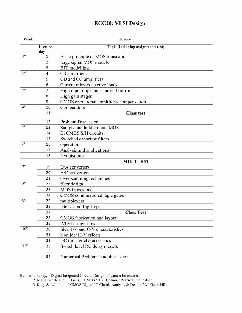
ECC20: VLSI Design
Week Theory
Lecture
day
Topic (Including assignment/ test)
1st 1. Basic principle of MOS transistor 2. large signal MOS models 3. BJT modelling
2nd 4. CS amplifiers 5. CD and CG amplifiers
6. Current mirrors – active loads 3rd 7. High input impedance current mirrors
8. High gain stages 9. CMOS operational amplifiers- compensation
4th 10. Comparators 11. Class test
12. Problem Discussion 5th 13. Sample and hold circuits MOS 14. Bi CMOS S/H circuits 15. Switched capacitor filters 6th 16. Operation 17. Analysis and applications 18. Nyquist rate a. MID TERM 7th 19. D/A converters
20. A/D converters 21. Over sampling techniques
8th 22. filter design
23. MOS transistors 24. CMOS combinational logic gates
9th 25. multiplexers 26. latches and flip-flops 27. Class Test
28. CMOS fabrication and layout 29. VLSI design flow
10th 30. Ideal I-V and C-V characteristics 31. Non ideal I-V effects 32. DC transfer characteristics
11th 33. Switch level RC delay models
34. Numerical Problems and discussion
Books: 1. Rabey, ``Digital Integrated Circuits Design,” Pearson Education.
2. N.H.E.Weste and D.Harris,`` CMOS VLSI Design,” Pearson Publication.
3. Kang & Leblebigi,`` CMOS Digital IC Circuit Analysis & Design,” McGraw Hill.

ECC20 - List of Experiment
1. To study I-V behavior of NMOS and PMOS transistor.
2. To perform transient analysis of CMOS Inverter and its symbol creation.
3. To perform AC, DC and transient analysis of voltage follower.
4. To design full adder using MOS transistor.
5. To design transmission gate using CMOS inverter.
6. To design XOR (logic gate) using Transmission gate.
7. To study step response of two stage amplifier.
8. To draw the layout of inverter and verify DRC.
9. To design layout of voltage follower and verify DRC.
10. To design layout of NAND/NOR gate.
Dr. Urvashi Bansal
Coordinator

ECC21: Computer Networks
Units Contents/topics Approximate
Number of
classes
Unit 1 Introduction: Network Topologies, Wired vs wireless Networks, LAN,
MAN, WAN, Internet, Intranet & Extranet, Connection-Oriented and
Connectionless Services, Need of Protocols
Assignment: Bridges, Hubs and Switches, Virtual LANs
8
Unit 2 Network Protocols: ALOHA, Carrier Sense Multiple Access Protocols,
Framing, One-Bit Sliding Window Protocol, Protocol Using Go Back
N, High-Level Data Link Control (HDLC)
Assignment: Protocol Using Selective Repeat
5
Unit 3 Congestion Control In Data Networks: Congestion Prevention Policies,
Congestion Control in Virtual-Circuit Subnets, Congestion Control in
Datagram Subnets, Effects of Congestion, Load Shedding, Jitter Control
Assignment: Congestion Control in Packet-Switching Networks
7
Unit 4a Routing Algorithms: The Optimality Principle, Shortest Path Routing,
Flooding, Distance Vector Routing, Link State Routing.
4
MID-SEM EXAMINATION
Unit 4b Routing Algorithm Contd.: Hierarchical Routing, Broadcast Routing,
Multicast Routing, Routing for Mobile Hosts, Routing in Ad Hoc
Networks
Assignment: Node Lookup in Peer-to-Peer Networks
6
Unit 5 TCP/IP: Overview of TCP/IP, TCP/IP reference Model, comparison of
OSI & TCP/IP, Internet Protocol & IP Addresses, Principles of
Internetworking, Internet Protocol Operation, ,.
Assignment: IPv6
6
Unit 6 Addressing, Subnetting, Address Resolution Protocol, Reverse Address
Resolution Protocol, Internet Control Message protocol, User Datagram
Protocol, Transmission Control protocol, Virtual Private Networks and
IP Security
4
Total Lectures: 40
Note: Test 1 syllabus is During/Completion of Unit II
Mid-Semester exam syllabus is Unit I, II and III
Test 2 syllabus is During/Completion of Unit V
Books:
1. Behrouz A. Forouzan, “Data Communications and Networking ,” Mc Graw Hill
Education.
2. J. Kurose, K. W. Ross, “Computer Networking: A Top-Down Approach Featuring the Internet,”
Addison-Wesley.
3. S. Keshav, “An engineering approach to computer networking: ATM networks, the internet, and
the telephone network,” Addison-Wesley.
4. L. L. Peterson and B. S. Davie, “Computer networks: a systems approach,” Morgan Kaufmann
Publishers.

5. W. Stallings, “Data and computer communications,” Prentice Hall India.
6. A. S. Tanenbaum, “Computer networks,” Prentice Hall India.
Evaluation Scheme: (25 marks)
i. Class tests : weightage- 10 marks
ii. Teacher Assessment Quality : weightage- 8 marks
iii. Assignment : weightage- 7 mark
Prof. Shree Prakash Singh
Course Coordinator
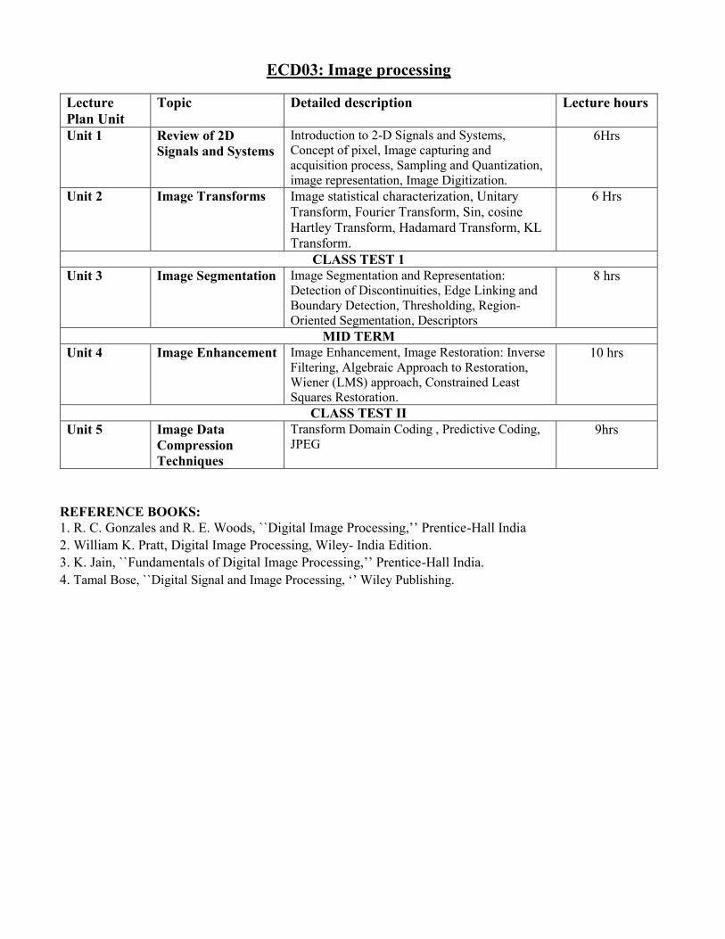
ECD03: Image processing
Lecture
Plan Unit
Topic Detailed description Lecture hours
Unit 1 Review of 2D
Signals and Systems
Introduction to 2-D Signals and Systems,
Concept of pixel, Image capturing and
acquisition process, Sampling and Quantization,
image representation, Image Digitization.
6Hrs
Unit 2 Image Transforms Image statistical characterization, Unitary
Transform, Fourier Transform, Sin, cosine
Hartley Transform, Hadamard Transform, KL
Transform.
6 Hrs
CLASS TEST 1
Unit 3 Image Segmentation Image Segmentation and Representation:
Detection of Discontinuities, Edge Linking and
Boundary Detection, Thresholding, Region-
Oriented Segmentation, Descriptors
8 hrs
MID TERM
Unit 4 Image Enhancement Image Enhancement, Image Restoration: Inverse
Filtering, Algebraic Approach to Restoration,
Wiener (LMS) approach, Constrained Least
Squares Restoration.
10 hrs
CLASS TEST II
Unit 5 Image Data
Compression
Techniques
Transform Domain Coding , Predictive Coding,
JPEG 9hrs
REFERENCE BOOKS:
1. R. C. Gonzales and R. E. Woods, ``Digital Image Processing,’’ Prentice-Hall India
2. William K. Pratt, Digital Image Processing, Wiley- India Edition.
3. K. Jain, ``Fundamentals of Digital Image Processing,’’ Prentice-Hall India.
4. Tamal Bose, ``Digital Signal and Image Processing, ‘’ Wiley Publishing.

List of Experiments:
1. Introduction to Digital Image Processing with Matlab. Types of Images, Interconversions of
formats, scaling, translation and rotation of image, histogram.
2. Convolution of 2 dimensional matrices with and without 2D DFT.
3. Fourier domain representation and analysis of images.
4. Types of noises (such as Gaussian noise, Rayleigh noise, salt and pepper noise etc.)and their
effect on images in spatial and spectral domain. Statistical noise models.
5. 2D filters and their usage for analyzing and transforming images.
6. Image Segmentation and Representation: Detection of Discontinuities, Edge Linking and
Boundary Detection.
7. Image Enhancement, Image Restoration: Inverse Filtering, Wiener (LMS) approach.
8. Image Data Compression Techniques, JPEG compression of images.
Prof. Jyotsna Singh
Course Coordinator

ECD-07: Analog Filter Design
Units Contents/topics Approximate
Number of
classes
Unit 1 An overview of history and progress of modern filter design; Five standard
filter functions; State variable synthesis of Multiple-op-amp biquads; Single
Op-Amp Biquads: Sallen-Key, Delyiannis-Friend Biquads; Review of the
concepts of sensitivity, Frequency transformations and impedance scaling
8
Unit 2 Active filter design based on passive ladder filter structures, Active filter
design using Inductor Substitution using Gyrator/GIC, Transformation of
elements using the concept of FDNR; Leap-Frog Ladder filters
6
Unit 3 Fully-Integratable Transconductance-C Filters: Transconductance Cells,
Various Transconductor Building Blocks- resistors, integrators, amplifiers,
summers, gyrators; First and second order OTA-C biquad filters, High order
OTA-C filters
6
MID-SEM EXAMINATION
Unit 4 Switched-Capacitor Filters: The MOS switch, The switched capacitor, first
order building blocks, second order sections, sampled data operation,
Switched-capacitor first and second order filters, Bilinear transformation
based SC filter design
4
Unit 5 Fully-integratable continuous-time MOSFET-C Filters: MOSFET-C
integrators and differentiators; MOSFET-C biquad Designs
4
Unit 6 Approximation Theory: Butterworth Approximation, Chebyshev
Approximation, Inverse Chebyshev Approximation
5
Unit 7 An overview of various active building blocks and their use in Filter design;
Fully-integratable filters suitable for Bipolar/CMOS technology
7
Suggested readings:
1. Gobind Daryanani, `Principles of active network synthesis and design,’ John Wiley and Sons
2. M.E. Van Valkenburg, `Analog Filter Design,’ Holt Saunders International Edition
3. Rolf Schaumann and Mac E. Van Valkenburg, `Design of Analog Filters, Oxford University Press
4. Other references suggested by the Course Instructor(s)
Evaluation Scheme: (15 marks)
iv. Class tests : weightage- 5 marks (Test-1 during/after Unit 2; Test 2-during or after
Unit 5)
v. Assignments : weightage- 5 marks
vi. Attendance : weightage- 5 marks

ECD-07 Analog Filter Design
Experiments:
I. Hardware Experiments:
1. Design and verification of Notch Filter using a simulated inductor
2. Single-op-amp based biquad design
3. Design of a LP/BP/ Filter using Tow-Thomas Biquad
4. Filter design using FDNR
5. Filter design using Norton amplifier LM3900
II. SPICE-based Experiments
6. CFOA-based Voltage-mode Filter Design
7. CCII-based Current-mode Filter Design
8. CCII-based Voltage-mode Filter Design
9. OTA-C-biquad Filter
10. MOSFET-C Filter design
Prof. Raj Senani
Coordinator

ECD09: Computer Architecture & Digital Hardware Design
Basics of Logic Design: Combinational logic, finite state machines, Finite state machine with Datapath,
Microprogram Control (5 lectures)
Processor Performance: metrics and calculations, performance equations, Amdahl's law (3 lectures)
Instruction Set Architecture: instruction set classifications, addressing modes, instruction encoding,
impact of high-level language and compilers (8 lectures)
Computer Arithmetic: binary number systems, floating-point numbers, operations on binary numbers,
implementations, ALU design, fast adder design (8 lectures)
CPU Design And Architecture: stages of execution, basic CPU organization, single-cycle and multiple-
cycle designs, microprogramming vs. hardwired control, interrupts (5 lectures)
Pipelining: dependencies, data and control hazards, resolving hazards, forwarding, exceptions, multiple-
functional-unit pipelines (5 lectures)
Advanced Pipelining and Instruction Level Parallelism: dynamic scheduling, branch prediction,
superscalar issue, compiler and architectural support for ILP, register renaming (5 lectures)
Memory Hierarchy: caches and cache hierarchies, cache organizations, cache performance, compiler
support for cache performance, main memory organization, virtual memory, TLBs, I/0 characteristics
of UO devices. (5 lectures)
Buses (at the "big picture" level). Polling, interrupt-driven UO, DMA. (3 lectures)
Reference Text:
1. Hennessy and Patterson, "Computer Architecture: A Quantitative Approach," Morgan Kaufmann
Publishers
2. Patterson and Hennessy, "Computer Organization and Design: The Hardware/Software
Interface," Morgan Kaufmann Publishers
3. Harris and Harris, “Digital Design and Computer Architecture”, Elsevier
4. Pong P. Chu, “FPGA Prototyping by VHDL Examples”, Wiley

ECD09 Computer Architecture and Digital Hardware Design Lab
Experiment 1 is to be performed on available 74 series inverter. Experiments 2-6 to be modeled using
VHDL and tested on the AkshayPatra CPLD platform. The rest should only be simulated.
1. Characterization of Logic Family. Find out logic threshold values and noise margins. Delay
time measurement of inverter using ring oscillator.
2. Design, model and test using VHDL, a Sign magnitude adder, BCD incrementor, Gray Counter
and LFSR based random number generator.
3. Design model and test using VHDL a PWM based LED Dimmer
4. Design model and test using VHDL a single switch and keypad matrix de-bouncing system.
5. Design and model using VHDL, the following LED multiplexing schemes: regular LED
multiplexing, Charlieplexed LED multiplexing.
6. Design, model and test using VHDL, a multi-stage Dice game.
7. VHDL behavioral model for a 32-bit MIPS ALU
8. VHDL model of a 5-stage CPU model
9. VHDL model for a pipelined processor
Mr. D. V. Gadre
Course Coordinator
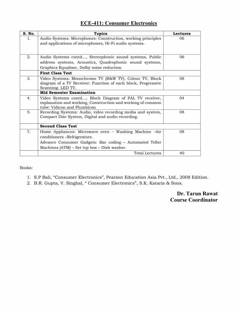
ECE-411: Consumer Electronics
S. No. Topics Lectures
1. Audio Systems: Microphones: Construction, working principles
and applications of microphones, Hi-Fi audio systems.
06
2. Audio Systems contd…, Stereophonic sound systems, Public
address systems, Acoustics, Quadrophonic sound systems,
Graphics Equaliser, Dolby noise reduction
06
First Class Test
3. Video Systems: Monochrome TV (B&W TV), Colour TV, Block
diagram of a TV Receiver: Function of each block, Progressive
Scanning. LED TV.
08
Mid Semester Examination
4. Video Systems contd…, Block Diagram of PAL TV receiver, explanation and working, Construction and working of common
tube: Vidicon and Plumbicon
04
5. Recording Systems: Audio, video recording media and system,
Compact Disc System, Digital and audio recording.
08
Second Class Test
7. Home Appliances: Microwave oven – Washing Machine –Air
conditioners –Refrigerators.
Advance Consumer Gadgets: Bar coding – Automated Teller
Machines (ATM) – Set top box – Dish washer.
08
Total Lectures 40
Books:
1. S.P Bali, “Consumer Electronics”, Pearson Education Asia Pvt., Ltd., 2008 Edition.
2. B.R. Gupta, V. Singhal, “ Consumer Electronics”, S.K. Kataria & Sons.
Dr. Tarun Rawat
Course Coordinator

M. Tech. Courses
Semester (January to May) 2018-2019
Lecture Plan

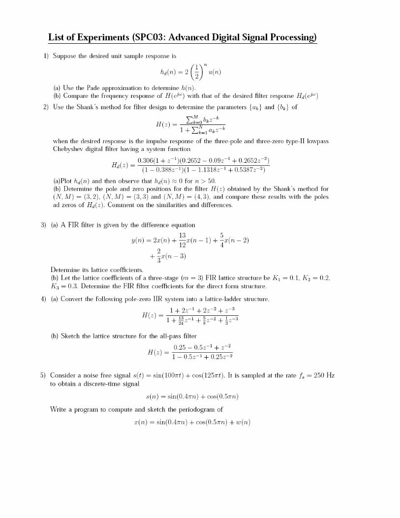
SPC03: Advanced Digital Signal Processing
S. No. Topics Lectures
1. Signal Modeling, All pole (AR), all zero(MA), pole zero models
(ARMA), Generation of random processes and whitening.
06
2. Prony’s method, Pade approximation, Shanks method. 06
First Class Test
3. Spectral factorization, Optimum linear filters, FIR and IIR. 08
Mid Semester Examination
4. Lattice structures, Forward and backward linear prediction,
The Levinson-Durbin algorithm.
06
5. Power Spectrum Estimation: Nonparametric methods 06
Second Class Test
7. Parametric methods, Eigenanalysis algorithms for spectrum
estimation: PHD, Eigen-decomposition, MUSIC, ESPRIT
algorithms.
08
Total Lectures 40
Books:
1. P. P. Vaidyanathan, “Multirate Systems and Filter Banks,” Prentice Hall.
2. S. K. Mitra, “Digital Signal Processing: A Computer Based Approach,”McGraw-Hill.
3. Tarun Kumar Rawat, “Digital Signal Processing,” Oxford University Press.

Prof. H. Parthasarthy
Course Coordinator

SPC04: Adaptive Signal Processing
S. No. Topics Lectures
1. Basic concepts of Adaptive Filtering. Mathematical
preliminaries, Review of Random signal theory, correlation
matrix and some linear algebra, KL expansion.
06
2. Mean-square error criterion, Wiener filters, principle of
orthogonality.
06
First Class Test
3. Wiener filters contd…, Gradient Search Algorithm (Newton),
Steepest Descent Algorithms, The LMS algorithm.
08
Mid Semester Examination
4. The LMS algorithm contd…, convergence, misadjustment,
Normalized LMS algorithm, Frequency domain LMS algorithm,
Block LMS.
06
5. Weighted Least squares algorithm, Recursive Least squares
algorithm Properties.
06
Second Class Test
7. RLS algorithm contd…, Kalman Filtering, Fundamentals of
array signal processing.
08
Total Lectures 40
Books:
1. B. Widrow and S. D. Stearns, “Adaptive Signal Processing,”Pearson Education.
2. B. Farhang-Boroujeny, “Adaptive Filters Theory and Applications,” John Wiley and
Sons.
3. Tarun Kumar Rawat, “Digital Signal Processing,” Oxford University Press.


SPD03: Analog IC for Signal Processing
Syllabus Details of
topics to
be
covered
Total hrs
for lectures
Introduction to MOSFET device structure and operation, MOS
as amplifier, Biasing in MOS amplifier circuits, small signal equivalent circuit model, Single stage MOS amplifiers,
characterizing amplifiers, MOS internal capacitance and high
frequency model, frequency response
Chapter 3
from book 3
06
IC biasing-current sources, current mirrors and current-
steering circuits, cascode and wilson current mirror Chapter from
4 book 3
05
First Class Test
Common Source, common gate and common drain IC
amplifiers, low frequency and high frequency response, noise
performance Multiple-Transistor IC amplifiers, Cascode configuration,
folded cascode and self cascode structure, Voltage follower,
flipped voltage follower
Chapter 4,5
from book 3
10
Mid Sem. Exam
MOS differential pair, small signal operation, differential gain,
common mode gain, common mode rejection ratio, active loaded differential amplifier
Chapter 5
from book 3
04
Frequency response, Noise Spectrum, sources, types, Thermal
and Flicker noise, representation in circuits, Noise bandwidth, Noise figure
Chapter 5
from book 3
04
CMOS analog integrated circuits, Op-amp design, op-amp
characteristics and model, DC offset and DC bias currents,
Gain, bandwidth and slew rate, Noise, Input stage, output
stage
Chapter 6,7
from book 3
06
Second Class Test
OTA, Operational Current amplifier design, Current trends in
Analog IC Design Chapter7
from book3
04
References:
1. Gregorian and Temes, “Analog MOS integrated circuits for signal processing,” John wiley
Publication.
2. Kenneth R. Laker and Willy M.C. Sansen, “Design of Analog Integrated Circuits and systems,”
McGraw-Hill.
3. Philip E. Allen & Douglas R. Holberg, “CMOS Analog Circuit Design,” Oxford University Press.
4. Behzad Razavi, “Design of Analog CMOS Integrated Circuit,” Tata McGraw Hill.
5. Gray R. Paul, Hurst J. Paul, Lewis H. Stephen and Meyer G. Robert, “Analysis and Design of
Analog Integrated Circuits”, John Wiley and Sons.
Dr. Shweta Gautam
Course Coordinator

SPD11: Digital Image Processing
Unit Topic Detailed description Lecture hours
Unit 1 Review of 2D
Signals and
Systems
Introduction to 2-D Signals and Systems, Image
capturing and acquisition process, Image Digitization,
image representation
6 Hrs
Unit 2 Image
Transforms
Image statistical characterization, Unitary Transform,
Fourier Transform, Sin, cosine Hartley Transform,
Hadamard Transform, KL Transform.
7 Hrs
CLASS TEST -I
Unit 3 Image
Segmentation
Image Segmentation and Representation: Detection of
Discontinuities, Edge and Boundary Detection,
Thresholding, Region-Oriented Segmentation,
Descriptors
10 hrs
MID SEMESTER TEST
Unit 4 Image
Enhancement
and Restoration
Image Enhancement, Image Restoration: Linear and
nonlinear Filtering, Algebraic Approach to
Restoration, Wiener (LMS) approach, Constrained
Least Squares Restoration.
10 hrs
CLASS TEST II
Unit 5 Image Data
Compression
Techniques
Transform Domain Coding , Linear Predictive Coding
and other recent image compression techniques
6 hrs
39 hours
REFERENCE BOOKS:
1. R. C. Gonzales and R. E. Woods, ``Digital Image Processing,’’ Prentice-Hall India
2. William K. Pratt, Digital Image Processing, Wiley- India Edition.
3. K. Jain, ``Fundamentals of Digital Image Processing,’’ Prentice-Hall India.
4. Tamal Bose, ``Digital Signal and Image Processing, ‘’ Wiley Publishing.
Prof. Jyotsna Singh
Course Coordinator

SPD15: Wireless Communication
1. INTRODUCTION 05
Evolution of various generations of Wireless Communication systems and standards, Fundamentals of
digital communication systems, Error performance of communication systems in an AWGN channel.
2. PRINCIPLES OF WIRELESS COMMUNICATIONS 07
Basics of wireless channel modelling, Fading, Delay spread, RMS delay spread, Coherence Bandwidth,
Doppler fading, Classification of fading channels: slow and fast fading, flat and frequency selective fading,
Rayleigh fading model.
3. SISO WIRELESS SYSTEMS OVER FADING CHANNELS 08
BER performance of wireless communication system over Rayleigh and Nakagami-m fading channels,
SNR in wireless systems, Concept of Diversity, Types of diversity, ML Detection and Channel Estimation
in wireless communications.
SISO WIRELESS SYSTEMS OVER FADING CHANNELS (Contd.) 04
Outgae Probability, Ergodic capacity, Calculation of outage probability and ergodic capacity for different
wireless communication systems, Asymptotic analysis
4. MULTIPLE ANTENNA BASED WIRELESS COMMUNICATIONS 08
Introduction to SIMO. MISO, and MIMO communication systems, Beamforming techniques, Diversity
combining techniques: Selection Combining, Maximal Ratio Combining, Equal Gain Combining, Error
and outage analysis of various MIMO systems over fading channels,
5. SPACE TIME BLOCK CODES 07
Introduction to Space-Time coding, Orthoganal STBC, Alamouti STBC, Performance of Alamouti STBC
over Rayleigh fading channel, ML Detection of OSTBC
Total Lectures: 39+1 (Class Test)
Books:
• Principles of Modern Wireless Communication Systems by Aditya K Jagannathamn
• Space-Time Block Coding for Wireless Communications by E. Larsson and P. Stoica
• Wireless Communications: Principles and Practice by Theodore S. Rappaport
MID SEMESTER EXAMINATION
CLASS TEST

List of Experiments to be performed during January - May 2019
(All the experiments will be performed on MATLAB software)
6. Simulate a wireless communication system with no fading over AWGN channel using different
modulation schemes.
7. Simulate the Rayleigh density function and verify with the analytical PDF.
8. Simulate the CDF of Nakagami-m distribution and verify with theoretical CDF.
9. Evaluate the BER performance of SISO wireless communication system over Rayleigh fading
channel
10. Analyze the outgae performance for Rayleigh faded wireless communication systems.
11. Analyze the ergodic capacity performance for Rayleigh faded wireless communication systems.
12. Observe the impact of transmit diversity on the error performance of wireless communication
system.
13. Analyze the error and outage performance of receive diversity using selection combining.
14. Compare the performance for selection combining and Maximal Ratio Combining techniques.
15. Simulate the 2 X 2 wireless communication system utilizing Alamouti STBC and plot the BER
versus SNR performance over Rayleigh fading channel.
Dr. Ankur Bansal
Course Coordinator
MID SEMESTER EXAMINATION

ESC03: Integrated Circuits for Analog Signal Processing
Week Theory
Lecture
day
Topic (Including assignment/ test)
1st 1. Different types of signals
2. Information
3. Interference and noise 2nd 4. Signal classification
5. Dynamic range
6. S/N ratio, 3rd 7. Functions in analog signal processing
8. Linear non-linear functions
9. Impedance adaptation 4th 10. Amplitude and level matching 11. Class test 12. Terminal matching, buffering filtering 5th 13. Linearization 14. Domain conversions 15. Errors in analog signal processing
6th 16. Voltage amplification 17. Practical voltage amplifiers 18. Effects of finite input impedances MID TERM 7th 19. Building blocks for voltage amplifiers
20. Current to voltage and voltage to current conversion
21. Current integrators, mirrors, amplifiers, conveyors
8th 22. Analog building blocks, Op-amp design
23. DC offset and DC bias currents
24. Gain, bandwidth and slew rate 9th 25. Noise in amplifier
26. CMOS OTA, ideal model, OTA building block circuits, design of simple OTA
27. Class Test
28. Signal rectifications, AC/DC conversion
29. CMOS implementation of adder 10th 30. Subtractor, squarer
31. Analog multiplier, analog dividers
32. Differentiator and integrator circuits 11th 33. Impedance transformation and conversion
34. Analog multiplexers
Books: 1. Pallas Areny and John G. Webster, “Analog Signal Processing,” John Wiley. 2. M. Ismail and T. Fiez, “Analog VLSI signal and Information processing,” Mc-Graw hill.
3. Philip E. Allen & Douglas R. Holberg, “CMOS Analog Circuit Design,” Oxford University Press.

ESC03 - List of Experiment
1. To study I-V behavior of NMOS and PMOS transistor with PMOS load.
2. To perform transient analysis of CMOS Opamp and its symbol creation.
3. To perform AC and DC analysis of OTA.
4. To perform noise analysis of an Opamp.
5. To realize a biquad filter using Opamp.
6. To realize integrator and differentiator using Opamp.
7. To verify dc characteristics of a current conveyor.
8. To draw the layout of inverter and verify DRC.
9. To design layout of voltage follower and verify DRC.
To design layout of NAND/NOR gate
Dr. Urvashi Bansal
Course Coordinator

ESC04: Processor Design
Embedded Computer Architecture Fundamentals: Components of an embedded computer, Architecture
organization, ways of parallelism, I/O operations and peripherals. (5 lectures)
Problems, Fallacies, and Pitfalls in Processor Design for a high level computer instruction set architecture
to support a specific language or language domain, use of intermediate ISAs to allow a simple machine to
emulate its betters, stack machines, overly aggressive pipelining, unbalanced processor design, Omitting
pipeline interlocks, Non- power-of-2 data-word widths for general-purpose computing (10 lectures)
Memory: Organization, Memory segmentation, Multithreading, Symmetric multiprocessing.Processor
Design flow: Capturing requirements, Instruction coding, Exploration of architecture organizations,
hardware and software development. Extreme CISC and extreme RISC, Very long instruction word
(VLIW). (10 lectures)
Digital signal processor: Digital signal processor and its design issues, evolving architecture of DSP, next
generation DSP.Customizable processors: Customizable processors and processor customization, A
benefit analysis of processor customization, use of microprocessor cores in SOC design, benefits of
microprocessor extensibility. (10 lectures)
Run time Re-configurable Processors: Run time Re-configurable Processors,Embedded microprocessor
trends, instruction set metamorphosis, reconfigurable computing, run-time reconfigurable instruction set
processors ,coarse grain reconfigurable processors,Processor Clock Generation and Distribution: Clock
parameters and trends, Clock distribution networks, de-skew circuits, jitter reduction techniques, low
power clock distribution. (10 lectures)
Asynchronous Processor Design: Asynchronous and self timed processor design, need of asynchronous
design, development of asynchronous processors, asynchronous design styles, features of asynchronous
design. (5 lectures)
ESC04: Processor Design Lab
1. Design, model and test using VHDL, a Sign magnitude adder, BCD incrementor, Gray Counter
and LFSR based random number generator.
2. Design model and test using VHDL a PWM based LED Dimmer
3. Design model and test using VHDL a single switch and keypad matrix de-bouncing system.
4. Design and model using VHDL, the following LED multiplexing schemes: regular LED
multiplexing, Charlieplexed LED multiplexing.
5. Design, model and test using VHDL, a multi-stage Dice game.
6. VHDL behavioral model for a 32-bit MIPS ALU
7. VHDL model of a 5-stage CPU model
8. VHDL model for a pipelined processor
Mr. D. V. Gadre
Course Coordinator
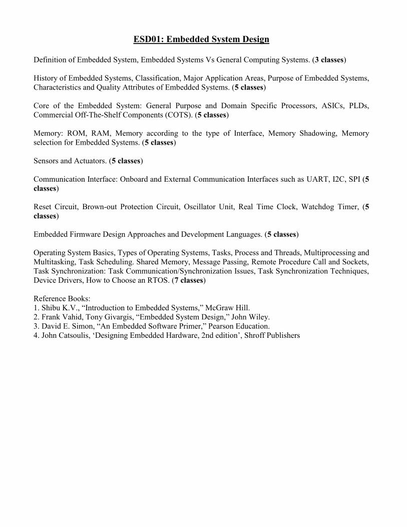
ESD01: Embedded System Design
Definition of Embedded System, Embedded Systems Vs General Computing Systems. (3 classes)
History of Embedded Systems, Classification, Major Application Areas, Purpose of Embedded Systems,
Characteristics and Quality Attributes of Embedded Systems. (5 classes)
Core of the Embedded System: General Purpose and Domain Specific Processors, ASICs, PLDs,
Commercial Off-The-Shelf Components (COTS). (5 classes)
Memory: ROM, RAM, Memory according to the type of Interface, Memory Shadowing, Memory
selection for Embedded Systems. (5 classes)
Sensors and Actuators. (5 classes)
Communication Interface: Onboard and External Communication Interfaces such as UART, I2C, SPI (5
classes)
Reset Circuit, Brown-out Protection Circuit, Oscillator Unit, Real Time Clock, Watchdog Timer, (5
classes)
Embedded Firmware Design Approaches and Development Languages. (5 classes)
Operating System Basics, Types of Operating Systems, Tasks, Process and Threads, Multiprocessing and
Multitasking, Task Scheduling. Shared Memory, Message Passing, Remote Procedure Call and Sockets,
Task Synchronization: Task Communication/Synchronization Issues, Task Synchronization Techniques,
Device Drivers, How to Choose an RTOS. (7 classes)
Reference Books:
1. Shibu K.V., “Introduction to Embedded Systems,” McGraw Hill.
2. Frank Vahid, Tony Givargis, “Embedded System Design,” John Wiley.
3. David E. Simon, “An Embedded Software Primer,” Pearson Education.
4. John Catsoulis, ‘Designing Embedded Hardware, 2nd edition’, Shroff Publishers

ESD01–Embedded System Design Lab The laboratory experiments for ESD01 will consist of:
1. Proposal of a standalone, microcontroller based hardware project that has suitable input and output
devices, sensors, intra-system communication protocols (I2C, SPI etc), memory storage device, power
supply and uses a modern microcontroller of your choice (AVR, MSP430, ARM Cortex M0, M3, M4
etc) and this should achieve something useful.
2. Gantt’s chart for implementing the proposed project during the course of the semester. This should
include tasks such as visualization of the project, schematic capture, PCB design and layout, PCB
fabrication, code development, project fabrication and integration, testing and final deployment as well
as complete documentation and 2-minute long YouTube video.
3. Design and fabrication of the PCB either through external PCB services or using the resources in CEDT.
4. Soldering and testing the project hardware.
5. Code integration and testing.
6. Final demonstration and submission.
List of Input, output, sensors and communication and memory storage devices:
• Inputs: switches, keypads, capacitive touch, joystick etc.
• Outputs: LED, SSD, LED Matrix, character and graphics LCD, DC/Stepper motor, relay, speaker etc.
• Sensors: temperature, humidity, magnetic field, light, pH, sound etc.
• Communication: UART, I2C, SPI, USB etc.
• Memory: serial flash memory devices.
Mr. D. V. Gadre
Course Coordinator

ESD05: Device Modelling and Circuit Simulation
S. No. Topics No of Hours
1. Overview of MOS transistor physics, Two-Terminal MOS structure, Flat -
band voltage 3 Hours
2. Effect of Gate-substrate voltage on surface condition, Inversion, Small
signal capacitance 4 Hours
3.
Three-Terminal MOS structure, Body effect, regions of inversion, Pinch-
off voltage, Four Terminal MOS Transistor, regions of inversion, charge
sheet model, interpolation model, body referenced model
4 Hours
Ist Unit Test
4.. MOS transistor large-signal modeling, quasi-static operation, limitations of
quasi-static model, introduction to non-quasi static model 4 Hours
MID TERM EVALUATION
5..
MOS transistor small-signal modeling, low & medium frequency model,
high frequency model, considerations in MOS modeling for RF
applications, gate resistance, transition frequency, maximum frequency of
oscillation,
Hours
6.. Noise model and calculation of noise in different circuits 6 Hours
7..
MOSFET modeling for circuit simulation, Types of models, system for data
acquisition and parameter extraction, properties of good models,
Introduction to SPICE modeling, modeling of resistor, capacitor, inductor,
diode, BJT, JFET, MOSFET, model parameters, Brief overview of BSIM
and EKV model, Device and process simulator
5 Hours
2nd Unit Test
8..
Circuit simulation techniques, DC analysis, AC analysis, transient analysis,
SPICE Modeling of Process Variation, Process corners, Monte Carlo
simulation, and sensitivity/worst case analysis
3 Hours
9. Simulation of digital and analog circuits, transfer function, frequency
response, Noise analysis, distortion and spectral analysis. 2 Hours
SUGGESTED READINGS:
1. Y. Tsividis, “Operation and modeling of MOS transistors,” McGRAW-Hill.
2. Paul W. Tuinenga, “SPICE: A Guide to Circuit Simulation and Analysis Using PSpice,” Pearson.
3. Paolo Antognetti and Giuseppe Massobrio, “Semiconductor Device Modeling with SPICE,”McGraw-HillM M
Mano, ``Digital logic and computer design ,’’ Prentica Hall India

Experiment List for ESD05
Exp 1: Implement OTA circuit in LTSPICE and perform DC, AC and Transient analysis.
Exp 2: Perform parametric analysis of OTA by varying its biasing Current, temperature, Aspect Ratio and
see their effect on gm, BW and operating range.
Exp 3: Perform MC analysis and Noise analysis of OTA circuit used in Exp1.
Exp 4: Using subckt command implement Op-Amp and then using the Op-Amp design an inverting
amplifier.
Exp 5: Design a 2:1 MUX using NOR gate
Exp 6: Design an Ackerberg-Mossberg bandpass using macro-model of Op-Amp.
Exp 7: Design LPF, HPF and BPF using macro model of Op-Amp and opamp0 model.
Exp 8: Design a grounded inductor using OTA macro model.
Dr. Bhawna Agarwal
Course Coordinator
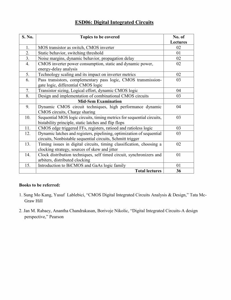
ESD06: Digital Integrated Circuits
S. No. Topics to be covered No. of
Lectures
1. MOS transistor as switch, CMOS inverter 02
2. Static behavior, switching threshold 01
3. Noise margins, dynamic behavior, propagation delay 02
4. CMOS inverter power consumption, static and dynamic power,
energy-delay analysis
02
5. Technology scaling and its impact on inverter metrics 02
6. Pass transistors, complementary pass logic, CMOS transmission-
gate logic, differential CMOS logic
03
7. Transistor sizing, Logical effort, dynamic CMOS logic 04
8. Design and implementation of combinational CMOS circuits 03
Mid-Sem Examination
9. Dynamic CMOS circuit techniques, high performance dynamic
CMOS circuits, Charge sharing
04
10. Sequential MOS logic circuits, timing metrics for sequential circuits,
bistability principle, static latches and flip flops
03
11. CMOS edge triggered FFs, registers, ratioed and ratioless logic 03
12. Dynamic latches and registers, pipelining, optimization of sequential
circuits, Nonbistable sequential circuits, Schmitt trigger
03
13. Timing issues in digital circuits, timing classification, choosing a
clocking strategy, sources of skew and jitter
02
14. Clock distribution techniques, self timed circuit, synchronizers and
arbiters, distributed clocking
01
15. Introduction to BiCMOS and GaAs logic family 01
Total lectures 36
Books to be referred:
1. Sung Mo Kang, Yusuf Lablebici, “CMOS Digital Integrated Circuits Analysis & Design,” Tata Mc-
Graw Hill
2. Jan M. Rabaey, Anantha Chandrakasan, Borivoje Nikolic, “Digital Integrated Circuits-A design
perspective,” Pearson

ESD06: Digital Integrated Circuits Lab
List of Experiments:
1. Implement a CMOS inverter and plot its transient and DC characteristics.
2. Implement a 3-input NAND gate and verify its functionality through transient analysis.
3. Implement a 2x1 multiplexer and verify its functionality through transient analysis.
4. Implement a CMOS circuit to realize the logic function F = A+BC+DE.
5. Implement dynamic and static D-Latch and D-Flip flop using pass transistor logic.
6. Implement a PowerPC based Transmission Gate Flip-flop (TGFF).
7. Implement a Toggle Flip-flop using TGFF and realize an 8-bit asynchronous counter.
8. Implement EXOR circuit using transmission gates and inverters and characterize for delay, power,
PDP and PDAP.
9. Determine the relationship between gate capacitance and transistor widths at 180nm TSMC CMOS
process technology.
10. Determine the transistor sizes of a 2x1 multiplexer (using only two input NAND gates) for
minimum power delay product (PDP) using Logical Effort theory at 16X capacitive load.
Dr. Kunwar Singh
Course coordinator