Embed Size (px)
Citation preview

8/7/2019 Electronics 1 Presentation Part 3 (ME)
http://slidepdf.com/reader/full/electronics-1-presentation-part-3-me 1/102
Semiconductor Diode
Circuit Analysis
Prepared by: Armando V. Barretto

8/7/2019 Electronics 1 Presentation Part 3 (ME)
http://slidepdf.com/reader/full/electronics-1-presentation-part-3-me 2/102
Load Line Analysis
• Below is a circuit which will be used to describe the operation of a diodecircuit.
• The diode in the circuit is forward biased.• The intersection of the characteristic curve of the diode and the load line
defines the current and voltage levels of the network.
Cathode (K)Anode (A)
ID
ID (mA)
VD
(V)
Quiescent Point (Q point)
Zener potential / voltage VZ
Zener region
Reversesaturationcurrent
ID (pA)
Load line
E R
E / R
Diodecharacteristiccurve
Q
EVDQ
IDQVR
VD

8/7/2019 Electronics 1 Presentation Part 3 (ME)
http://slidepdf.com/reader/full/electronics-1-presentation-part-3-me 3/102
Load Line Analysis
• Applying Kirchhoff’s voltage law in the clockwise direction, the followingequation can be derived:
• Based on the equation above, if VD is equal to zero, ID = E / R.
• Also, if ID is equal to zero, VD = E.
• A straight line drawn between the two points defined when VD = 0 and ID = 0yields the load line of the network.
• The point of intersection between the straight line and the characteristic curve
of the diode is the point of operation of the network, and it is called theQuiescent (Q) point.
• The value of the current I D can be computed as:
• The above two equations can be solved simultaneously to determine unknown
parameters, although this process could be cumbersome.
RIVE 0VVE DDRD
R
VEI
D D
ID = IS (eVD /nVT-1)

8/7/2019 Electronics 1 Presentation Part 3 (ME)
http://slidepdf.com/reader/full/electronics-1-presentation-part-3-me 4/102
Diode Circuit Analysis
• An easier approach is to use approximate analysis in which we assume that the
voltage across a diode is fixed once it is forward biased.
• For a forward biased diode, the voltage drop across the diode can be assumedto be:
0.7 volt for Silicon
0.3 volt for Ge1.2 volt for GaAs
• Example: With the circuit in the preceding slides having the followingparameters, determine the quiescent voltage and current of the diode.
E = 8 volts R = 4,700 ohms
volt0.7V
Ax101.5534700
0.7-8
R
V-EII
RIVE
Silicon),betoassumedis(diodevolt0.7isdiodethe
acrossdropvoltagethat theassumeweapproach,eapproximattheUsing
DQ
3DDQD
DD
8/7/2019 Electronics 1 Presentation Part 3 (ME)
http://slidepdf.com/reader/full/electronics-1-presentation-part-3-me 5/102
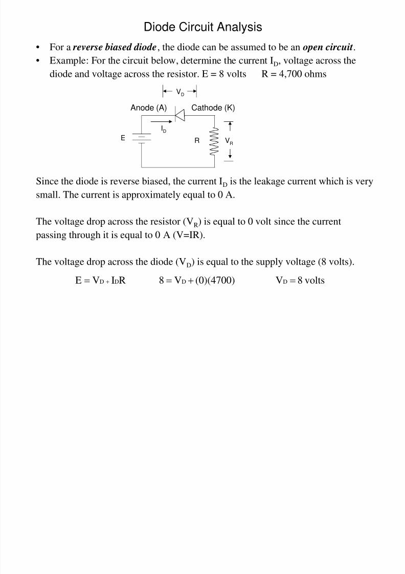
Diode Circuit Analysis
• For a reverse biased diode, the diode can be assumed to be an open circuit.
• Example: For the circuit below, determine the current ID, voltage across the
diode and voltage across the resistor. E = 8 volts R = 4,700 ohms
Since the diode is reverse biased, the current ID is the leakage current which is very
small. The current is approximately equal to 0 A.
The voltage drop across the resistor (VR) is equal to 0 volt since the current
passing through it is equal to 0 A (V=IR).
The voltage drop across the diode (VD) is equal to the supply voltage (8 volts).
Cathode (K)Anode (A)
IDE R VR
VD
volts8V (0)(4700)V8 RIVE DDDD

8/7/2019 Electronics 1 Presentation Part 3 (ME)
http://slidepdf.com/reader/full/electronics-1-presentation-part-3-me 6/102
Diode Circuit Analysis• Kircchoff’s voltage law is always applicable under any circumstances –
whether the voltages are dc, ac, pulses, or instantaneous values.• Example: For the circuit below, determine the current ID, voltage across the
diode and voltage across the resistor. E = 0.4 volt R = 4,700 ohms
Since the applied voltage (E) is less than 0.7 volt, it is not sufficient to turn on the
diode and the current will be approximately 0 A.
The voltage drop across the resistor (VR) is equal to 0 volt since the current
passing through it is equal to 0 A (V=IR).
The voltage drop across the diode (VD) is equal to the supply voltage (0.4 volt).
Cathode (K)Anode (A)
IDE R VR
VD
volt4.0V (0)(4700)V0.4 RIVE DDDD

8/7/2019 Electronics 1 Presentation Part 3 (ME)
http://slidepdf.com/reader/full/electronics-1-presentation-part-3-me 7/102
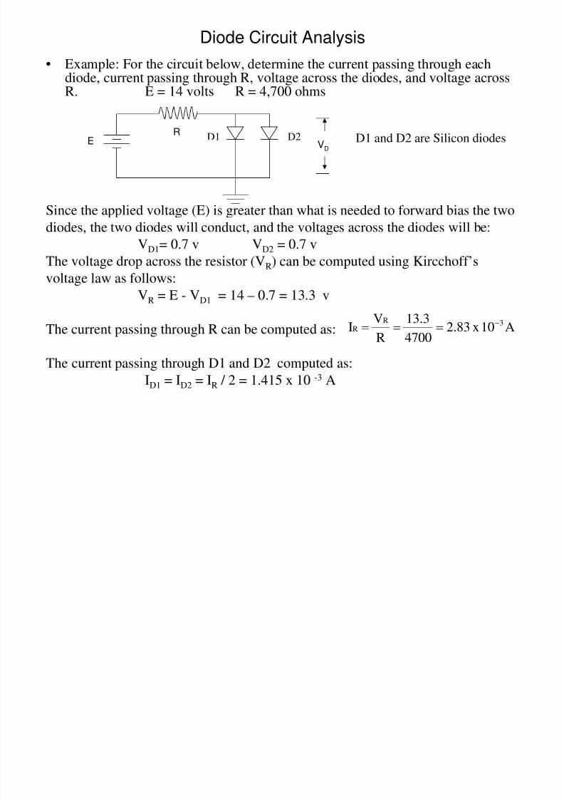
Diode Circuit Analysis• Example: For the circuit below, determine the current ID, voltage across the
diodes and voltage across the resistor. E = 14 volts R = 4,700 ohms
Since the applied voltage (E) is greater than what is needed to forward bias the twodiodes, the two diodes will conduct, and the voltages across the diodes will be:
VD1= 0.7 v VD2 = 1.8 volts
The voltage drop across the resistor (VR) can be computed using Kircchoff’svoltage law as follows:
VR = E - VD1 - VD2 = 14 – 0.7 – 1.8 = 11.5 v
The current across the loop can be computed as:
IDE R VR
VD2
A10x2.4474700
5.11
R
VI 3R
D
VD1
D1 D2
D1 is a Silicon diode
D2 is a red LED
8/7/2019 Electronics 1 Presentation Part 3 (ME)
http://slidepdf.com/reader/full/electronics-1-presentation-part-3-me 8/102
Diode Circuit Analysis
• Example: For the circuit below, determine the current passing through each
diode, current passing through R, voltage across the diodes, and voltage acrossR. E = 14 volts R = 4,700 ohms
Since the applied voltage (E) is greater than what is needed to forward bias the two
diodes, the two diodes will conduct, and the voltages across the diodes will be:VD1= 0.7 v VD2 = 0.7 v
The voltage drop across the resistor (VR) can be computed using Kircchoff’s
voltage law as follows:
VR = E - VD1 = 14 – 0.7 = 13.3 v
The current passing through R can be computed as:
The current passing through D1 and D2 computed as:
ID1 = ID2 = IR / 2 = 1.415 x 10 -3 A
E VD
A10x83.24700
3.13
R
VI 3R
R
D1 and D2 are Silicon diodesD1 D2R

8/7/2019 Electronics 1 Presentation Part 3 (ME)
http://slidepdf.com/reader/full/electronics-1-presentation-part-3-me 9/102
Rectifiers Using Semiconductor
Diodes
Prepared by: Armando V. Barretto

8/7/2019 Electronics 1 Presentation Part 3 (ME)
http://slidepdf.com/reader/full/electronics-1-presentation-part-3-me 10/102
Half Wave Rectifier Using Semiconductor Diode• A rectifier is a circuit which converts an alternating voltage into a pulsating dc
voltage.
• Rectifiers are used in power supplies to convert ac voltages to dc voltages.
• The power available from electric power companies are supplied using ac voltages
but many electrical and electronic devices need dc voltages, so there is a need to
convert ac voltages to dc voltages.
• A half-wave rectifier produces an output voltage during one-half (1800 ) of the input
ac signal. One half of the input signal is removed to establish a dc voltage.
• A half-wave rectifier using a semiconductor diode is shown below.
KA
IRL
AC Inputvoltage
(sine wave) RL
VO = output voltage(Pulsating DC voltage)
Half Wave Rectifier Using Semiconductor Diode
t
V
Input (Sine Wave)
t
V
Output (Pulsating DC)
Vp
Vp
Io

8/7/2019 Electronics 1 Presentation Part 3 (ME)
http://slidepdf.com/reader/full/electronics-1-presentation-part-3-me 11/102
Half Wave Rectifier Using Semiconductor Diode
• In practically all rectifier applications, the peak voltage of the input signal is much greater than the minimum voltage required to forward biased the diode.
• During the positive half , the diode becomes forward biased when the ac inputsignal becomes 0.7 volt (for Si), and it conducts.
– The input voltage practically appears across R during the positive half .
– The peak voltage of the output signal is approximately equal to the peakvoltage of the input signal (Vp of input signal minus 0.7 v).
• During the negative half , the diode is reverse biased and does not conduct.Output voltage across R is equal to 0 volt.
• The average value (Vdc) of the input signal is equal to zero because thealgebraic sum of the positive half and negative half is equal to zero.
Vdc(input) = 0 volt (for sine wave input signal) = average voltage of input
• The peak voltage of the output of a half wave rectifier is approximately equal to the peak voltage of the input signal .
Vp(out) = Vp(input) = peak voltage of output signal

8/7/2019 Electronics 1 Presentation Part 3 (ME)
http://slidepdf.com/reader/full/electronics-1-presentation-part-3-me 12/102
Half Wave Rectifier Using Semiconductor Diode
• If the voltage drop across the diode is ignored, the average value of the output voltage (Vo) and output current (Io) can be computed as:
rectifierwavehalf of currentoutputaverageR
Vp318.0
R
Vdc
Idc
rectifierwavehalf of tageoutput volaverageVp318.0Vp
Vdc
(1)(-1)-Vp210coscosVp
21
)cos(Vp2
1)(d)sin(Vp
T
1Vdc
LL
00
t t t
V
Vp
0 2
Half Wave Rectifier Output
Vdc
T
T = 2 = period
Vdc = average voltage
Vp = peak voltage

8/7/2019 Electronics 1 Presentation Part 3 (ME)
http://slidepdf.com/reader/full/electronics-1-presentation-part-3-me 13/102
Half Wave Rectifier Using Semiconductor Diode• If the voltage drop across the diode is ignored, the effective or rms value of the
output voltage (Vo) and output current (Io) of a half wave rectifier can becomputed as:
rectifierwavehalf of currentoutputeffectiveorrmsR
Vp0.5
R
VrmsIrms
rectifierwavehalf of tageoutput voleffectiveorrmsVp0.52
VpVrms
2
)0sin(0
2
)2sin(
4
Vp
2
)2sin(
04
Vp
)(d)2cos(14
Vp
)(d2
)2cos(1
2
Vp
)(d)sin(2
Vp)(d)sin(Vp
T
1Vrms
LL
22
0
2
0
2
0
22
0
2
t t
t t t
t
t t t t
VVp
0 2
Half Wave Rectifier Output
T = 2 = period of output voltage
Vdc = average output voltage
Vp = peak voltage
rms – root mean squareT

8/7/2019 Electronics 1 Presentation Part 3 (ME)
http://slidepdf.com/reader/full/electronics-1-presentation-part-3-me 14/102
Half Wave Rectifier Using Semiconductor Diode
• If there is no capacitor connected at the output of the rectifier,
– the maximum reverse bias voltage that will appear across the diode is
equal to the peak voltage of the input to the rectifier. This will occur
during the negative half of the input signal.
– the peak inverse voltage (PIV) or the peak reverse voltage (PRV) of thediode must be greater than the peak voltage of the input signal .
rectifier)of outputatconnectediscapacitorno(if VpPIV
KA
IRL
AC Inputvoltage
(sine wave) RL
VO = output voltage(Pulsating DC voltage)
Half Wave Rectifier Using Semiconductor Diode
t
V
Input (Sine Wave)
Vp
VD
t
V
Output (Pulsating DC)
Vp
Io

8/7/2019 Electronics 1 Presentation Part 3 (ME)
http://slidepdf.com/reader/full/electronics-1-presentation-part-3-me 15/102

8/7/2019 Electronics 1 Presentation Part 3 (ME)
http://slidepdf.com/reader/full/electronics-1-presentation-part-3-me 16/102
Half Wave Rectifier Using Semiconductor Diode
KA
IRL
AC Inputvoltage
(sine wave) RL
VO = output voltage(Almost pure DC voltage)
Half Wave Rectifier Using Semiconductor Diode And Capacitor Filter
Capacitor dischargingCapacitor charging
Output Voltage of Half Wave RectifierBefore Filtering
Output Voltage of Capacitor Filter Used WithHalf Wave Rectifier
Vp = peak voltageVp = peak voltage
+
-
signal)inputof half negative(during2VpVD
VD
Io

8/7/2019 Electronics 1 Presentation Part 3 (ME)
http://slidepdf.com/reader/full/electronics-1-presentation-part-3-me 17/102
Full Wave Rectifier Using Center Tapped Transformer• A full-wave rectifier produces an output voltage during the entire cycle (3600 ) of
the input ac signal.
• A full-wave rectifier using two semiconductor diodes and a center tapped
transformer is shown below.
AC Inputvoltage
(sine wave)
VO = output voltage(Pulsating DC voltage)
Full Wave Rectifier Using Semiconductor Diode and Center Tapped Transformer
t
Voltage at Secondary
Vpsec
+
-
D1
D2
I-I-
I-
I-
I+
I+
I+
I-
I+
I-
Vp1/2sec
Vp1/2sec
tVoltage At Each Half (½)
of Secondary
Vp1/2secV1/2sec
V1/2sec
Vo = Output
(Pulsating DC)
Vp1/2sec
Io= output current
I+ = current during positive half
I- = current during negative half
RL
Io

8/7/2019 Electronics 1 Presentation Part 3 (ME)
http://slidepdf.com/reader/full/electronics-1-presentation-part-3-me 18/102
Full Wave Rectifier Using Center Tapped Transformer• During the positive half of the voltage at the secondary of the transformer, D1 is
forward biased while D2 is reverse biased.– D1 conducts and current flows from the upper portion of secondary, to D1, to
RL, and then to the center tap of the transformer.
– The voltage at one half of the secondary appears across RL except for a small
voltage drop across D1.– The peak voltage at the output (Vpout) is almost equal to the peak voltage of
one half of the secondary voltage.
• During the negative half of the voltage at the secondary of the transformer, D2 is forward biased while D1 is reverse biased.
– D2 conducts and current flows from the lower portion of secondary, to D2, toRL, and then to the center tap of the transformer.
– The voltage at one half of the secondary appears across RL except for a smallvoltage drop across D2.
– The peak voltage at the output (Vpout) is almost equal to the peak voltage of one half of the secondary voltage.
• The average value (Vdc) of the input signal (voltage at ½ of secondary) is equal to zero because the algebraic sum of the positive half and negative half is equal to zero.
Vdc = 0 volt (for sine wave input signal)

8/7/2019 Electronics 1 Presentation Part 3 (ME)
http://slidepdf.com/reader/full/electronics-1-presentation-part-3-me 19/102
Full Wave Rectifier Using Center Tapped Transformer• If the voltage drops across the diodes are ignored, the average value of the
output voltage (Vo) and output current (Io) can be computed as:
V
Vp1/2sec
0 2
Full Wave Rectifier Using Center Tapped Transformer Output
Vdc
T
T = = period of output voltage
Vdc = average output voltage
Vp1/2sec = Vpsec /2 = peak voltage of 1/2 of secondary
Vpsec = peak voltage of whole secondary
rtransfomecenter tapusingrectifierwavefullof currentoutputaverage
RVp636.0
RVdc Idc
rtransfomecenter tapusingrectifierwavefullof tageoutput volaverage
Vp636.02Vp
Vdc
(1)(-1)-Vp1
0coscosVp1
)cos(Vp1
)(d)sin(VpT
1Vdc
L
sec1/2
L
sec1/2sec1/2
sec1/2sec1/2
0sec1/2
0sec1/2
t t t

8/7/2019 Electronics 1 Presentation Part 3 (ME)
http://slidepdf.com/reader/full/electronics-1-presentation-part-3-me 20/102
Full Wave Rectifier Using Center Tapped Transformer
• If the voltage drops across the diodes are ignored, the effective or rms value of
the output voltage (Vo) and output current (Io) of a full wave rectifier using
center tapped transformer can be computed as:
ertransformcenter tapusingrectifierwavefullof currentoutputeffectiveorrms
R
Vp0.707
R2
Vp
R
VrmsIrms
ertransformcenter tapusingrectifierwavefullof tageoutput voleffectiveorrms
Vp0.7072
VpVrms
2
)0sin(02
)2sin(2
Vp2
)2sin(
02Vp
)(d)2cos(12
Vp )(d
2
)2cos(1Vp
)(d)sin(
Vp
)(d)sin(VpT
1
Vrms
L
1/2sec
L
1/2sec
L
1/2sec1/2sec
21/2sec
21/2sec
0
21/2sec
0
21/2sec
0
22
1/2sec
0
2
1/2sec
t t
t t t t
t t t t

8/7/2019 Electronics 1 Presentation Part 3 (ME)
http://slidepdf.com/reader/full/electronics-1-presentation-part-3-me 21/102
Full Wave Rectifier Using Center Tapped Transformer
• If there is no filter capacitor connected at the output of the rectifier, the peak
inverse voltage (PIV) or the peak reverse voltage (PRV) of the diode mustbe greater than approximately two times the peak voltage of half of the
secondary or the peak voltage of the whole secondary of the transformer.
rectifier)of outputatconnectediscapacitorno(if Vp2
rectifier)of outputatconnectediscapacitorno(if VpsecPIV
sec1/2
AC Inputvoltage
(sine wave)
VO = output voltage(Pulsating DC voltage)
+
-
D1
D2
I-I-
I-
I-
I+
I+
I+
I-
I+
I-
Vp1/2sec
V1/2sec
V1/2sec
Vp1/2sec
Io= output current
I+ = current during positive half
I- = current during negative half
RL
t
Voltage at Secondary
Vpsec
Vp1/2sec
t
Voltage At Each Half (½)
of Secondary
Vp1/2sec
Vo = Output(Pulsating DC)
Io

8/7/2019 Electronics 1 Presentation Part 3 (ME)
http://slidepdf.com/reader/full/electronics-1-presentation-part-3-me 22/102
Full Wave Rectifier Using Center Tapped Transformer
• If a capacitor filter is connected at the output of the rectifier, the output voltage
will be different.• The output voltage of a full wave rectifier and output voltage of a capacitor filter
connected to a full wave rectifier are shown below.
• The output voltage of the filter is a dc voltage with some ripple (ac variation).
• When the output of the rectifier is increasing, the capacitor is charging, and
when the output of the rectifier is decreasing, the capacitor is discharging
through the load of the filter (RL).
• If the capacitor has no load , the output of the capacitor filter will ideally be a
constant dc voltage, because it will not be discharging.
Capacitor DischargingCapacitor charging
Output Voltage of Full Wave RectifierBefore Filtering
Output Voltage of Capacitor Filter Used WithFull Wave Rectifier
Vp1/2secVp1/2sec

8/7/2019 Electronics 1 Presentation Part 3 (ME)
http://slidepdf.com/reader/full/electronics-1-presentation-part-3-me 23/102
Full Wave Rectifier Using Center Tapped Transformer
• Whether there is a capacitor connected or no capacitor connected to theoutput of the rectifier, the voltage that will appear across the diode when it is
reverse biased is equal to two times the peak voltage of half of the secondary(2Vp1/2sec ) or the voltage of the whole secondary (Vpsec).
• If there is a filter capacitor connected at the output of the rectifier, the peak
inverse voltage (PIV) or the peak reverse voltage (PRV) of the diode mustalso be greater than approximately two times the peak voltage of half of the
secondary (2Vp1/2sec ) or the peak voltage of the whole secondary (Vpsec) of the transformer.
rectifier)of outputatconnectediscapacitor(if Vp2
rectifier)of outputatconnectediscapacitor(if VpsecPIV
sec1/2

8/7/2019 Electronics 1 Presentation Part 3 (ME)
http://slidepdf.com/reader/full/electronics-1-presentation-part-3-me 24/102
Full Wave Bridge Rectifier• A full-wave bridge rectifier using semiconductor diodes is shown below.
Full Wave Bridge Rectifier Using Semiconductor Diode
t
Voltage at Secondary
Vpsec
Vpsec
Vo = Output Voltage
(Pulsating DC)
Vo =
output
Voltage
D1D2
D3
D4
+
-
RL
Current flow during positive half of input signal
Current flow during negative half of input signal
Io =
output
current

8/7/2019 Electronics 1 Presentation Part 3 (ME)
http://slidepdf.com/reader/full/electronics-1-presentation-part-3-me 25/102
Full Wave Bridge Rectifier• During the positive half of the voltage at the secondary of the transformer, D2 and
D3 are forward biased while D1 and D4 are reverse biased.– D2 and D3 conduct and current flows from the upper portion of secondary, to
D2, to RL, to D3, and then to the lower portion of the secondary of thetransformer.
– The voltage at the secondary appears across RL
except for a small voltage dropacross D2 and D3.
– The peak voltage at the output (Vpout) is almost equal to the peak voltage of the secondary of the transformer.
• During the negative half of the voltage at the secondary of the transformer, D1 and
D4 are forward biased while D2 and D3 are reverse biased.– D1 and D4 conduct and current flows from the lower portion of secondary, to
D4, to RL, to D1, and then to the upper portion of the secondary of thetransformer.
– The voltage at the secondary appears across RL
except for a small voltage dropacross D1 and D4.
– The peak voltage at the output (Vpout) is almost equal to the peak voltage of the secondary of the transformer.

8/7/2019 Electronics 1 Presentation Part 3 (ME)
http://slidepdf.com/reader/full/electronics-1-presentation-part-3-me 26/102
Full Wave Bridge Rectifier• If the voltage drops across the diodes are ignored, the average value of the
output voltage (Vo) and output current (Io) can be computed as:
V
Vpsec
0 2
Full Wave Bridge Rectifier Output
Vdc
T
T = = period of output voltage
Vdc = average output voltage
Vpsec = peak voltage of secondary
rectifierbridgewavefullof currentoutputaverage
RVp636.0
RVdc Idc
rectifierbridgewavefullof tageoutput volaverage
Vp636.02Vp
Vdc
(1)(-1)-Vp1
0coscosVp1
)cos(Vp1
)(d)sin(VpT
1Vdc
L
sec
L
secsec
secsec
0sec
0sec
t t t

8/7/2019 Electronics 1 Presentation Part 3 (ME)
http://slidepdf.com/reader/full/electronics-1-presentation-part-3-me 27/102
Full Wave Bridge Rectifier
• If the voltage drops across the diodes are ignored, the effective or rms value of
the output voltage and output current of a full wave bridge rectifier can be
computed as:
rectifierbridgewavefullof currentoutputeffectiveorrms
R
Vp0.707
R2
Vp
R
VrmsIrms
rectifierbridgewavefullof tageoutput voleffectiveorrms
Vp0.7072
VpVrms
2
)0sin(02
)2sin(
2
Vp
2
)2sin(
02
Vp
)(d)2cos(12
Vp )(d
2
)2cos(1Vp
)(d)sin(Vp
)(d)sin(Vp
T
1Vrms
L
sec
L
sec
L
secsec
2sec
2sec
0
2sec
0
2sec
0
22
sec
0
2sec
t
t
t t t t
t t t t

8/7/2019 Electronics 1 Presentation Part 3 (ME)
http://slidepdf.com/reader/full/electronics-1-presentation-part-3-me 28/102
Full Wave Bridge Rectifier• If there is a filter capacitor or no filter capacitor connected at the output of the
rectifier, the voltage that will appear across the reverse biased diodes will be approximately equal to the peak voltage of the secondary.
• If there is no filter capacitor connected at the output of the rectifier, the peakinverse voltage (PIV) or the peak reverse voltage (PRV) of the diode must be
greater than approximately the peak voltage of the secondary of thetransformer.
• If there is a filter capacitor connected at the output of the rectifier, the peakinverse voltage (PIV) or the peak reverse voltage (PRV) of the diode must alsobe greater than approximately the peak voltage of the secondary of thetransformer.
rectifier)of outputatconnectediscapacitorno(if VpsecPIV
rectifier)of outputatconnectediscapacitor(if VpsecPIV

8/7/2019 Electronics 1 Presentation Part 3 (ME)
http://slidepdf.com/reader/full/electronics-1-presentation-part-3-me 29/102
Rectifiers
• If the voltage drops across the diodes are considered, the voltage drops
across the conducting diodes must be subtracted from the peak voltages in
the equations for the average voltage (Vdc) or rms voltages (Vrms) at the
output of the rectifier.
• Example: For a half wave rectifier with Silicon diode, the equation for the
average voltage if the voltage drop across the diode is considered will be:
• Example: For a full wave bridge rectifier with Silicon diodes, the equation
for the rms voltage (Vrms) if the voltage drop across the diodes is
considered will be:
0.7)(Vp0.318Vdc
)4.1(Vp0.707Vrms

8/7/2019 Electronics 1 Presentation Part 3 (ME)
http://slidepdf.com/reader/full/electronics-1-presentation-part-3-me 30/102
Comparison of RectifiersHalf wave rectifiers:
• Advantage is only one diode is used .
• Disadvantages compared to full wave rectifiers are:
– lower rms output voltage and lower average output voltage
– Higher ripple
Full wave rectifier with center tapped transformer:
• Advantage over bridge rectifier is only two diodes are used.
• Disadvantages compared to bridge rectifier assuming the same voltages at
whole secondary are:– lower rms output voltage and lower average output voltage (1/2 of bridge
rectifier)
Full wave rectifier with center tapped transformer:• Advantage is higher rms output voltage and higher average output voltage
(assuming the same voltage at whole secondary).
• Disadvantage is four diodes are used.

8/7/2019 Electronics 1 Presentation Part 3 (ME)
http://slidepdf.com/reader/full/electronics-1-presentation-part-3-me 31/102
Positive and Negative Voltages Power Supply• Below is a circuit which could be used to produce a positive and a negative
voltage using a transformer with center tap.
• During the positive half of the voltage at the secondary of the transformer, D1and D2 conducts, and C1 and C2 are charged with the polarity shown.
• During the negative half of the ac voltage at the secondary of the transformer,no diode conducts.
I2
0 volt
+ Output Voltage
- Output Voltage
+
-
-
+
D1
D2
C1
C2
P i i d N i V l P S l

8/7/2019 Electronics 1 Presentation Part 3 (ME)
http://slidepdf.com/reader/full/electronics-1-presentation-part-3-me 32/102
Positive and Negative Voltages Power Supply
• Below is a circuit which could be used to produce a positive dc voltage and a
negative dc voltage using a transformer with center tap.• During the positive half of the voltage at the secondary of the transformer, D2
and D3 conducts, and C1 and C2 are charged with the polarity shown.
• During the negative half of the ac voltage at the secondary of the transformer,D4 and D1 conducts, and C1 and C2 are charged with the polarity shown.
0 volt
+ Output Voltage
- Output Voltage
D1 D2
D3 D4
+
-
-
+
C1
C2
P iti d N ti V lt P S l

8/7/2019 Electronics 1 Presentation Part 3 (ME)
http://slidepdf.com/reader/full/electronics-1-presentation-part-3-me 33/102
Positive and Negative Voltages Power Supply
• Below is a circuit which could be used to produce a positive dc voltage and a
negative dc voltage using a transformer with no center tap.• During the positive half of the voltage at the secondary of the transformer, D1
conducts, and C1 is charged with the polarity shown.
• During the negative half of the ac voltage at the secondary of the transformer,D2 conducts, and C2 is charged with the polarity shown.
I2
0 volt
+ Output Voltage
- Output Voltage
+
-
-
+
D1
D2
D1 is conducting
D2 is conducting
C1
C2
T f

8/7/2019 Electronics 1 Presentation Part 3 (ME)
http://slidepdf.com/reader/full/electronics-1-presentation-part-3-me 34/102
Transformers• Transformers are typically used to step up or step down the primary voltage, or
match a load impedance.• A transformer can increase or decrease the voltage or current levels on the
secondary depending on the turns ratio of the primary and secondary.
• A transformer can also increase or decrease the impedance of the load
appearing at the primary of the transformer depending on the square of the
transformer turns ratio.
• Turns ratio is equal to the number of turns in the primary divided by the
number of turns in the secondary.
• The turns ratio can be used to match the impedance of the load (RL
) to the
output impedance of the amplifier.
Transformers

8/7/2019 Electronics 1 Presentation Part 3 (ME)
http://slidepdf.com/reader/full/electronics-1-presentation-part-3-me 35/102
Transformers• Assuming that the transformer is lossless (no power is dissipated in the
transformer), the following relationships can be derived:
RL =
R2
Transformer
N1:N2
V1 V2
secondaryatcurrentI
primaryatcurrentI
ertransformtheof impedanceloadRR
primaryat theRof impedancereflected
ertransformtheof primaryat theimpedanceinputR
secondaryat thevoltageaverageV
primaryat thevoltageaverageV
secondaryat thegepeak voltaV
primaryat thegepeak voltaV
secondaryat thevoltagermsV
primaryat thevoltagermsV
secondaryin theturnsof numberN
primaryin theturnsof numberN:where
ertransformof ratioturnsaR
R
I
I
V
V
V
V
V
V
N
N
2
1
L2
2
1
dc2
dc1
p2
p1
rms2
rms1
2
1
2
1
1
2
dc2
dc1
p2
p1
rms2
rms1
2
1
R1
I1
I2
2
2
2
1
2
1
2
1
22
11
2
1a
N
N
N
N
N
N
/IV
/IV
R
R
V l A d C R l i hi F A Si W

8/7/2019 Electronics 1 Presentation Part 3 (ME)
http://slidepdf.com/reader/full/electronics-1-presentation-part-3-me 36/102
Voltage And Current Relationships For A Sine Wave• For a sine wave with a peak voltage = Vp, the rms voltage, rms current, average
voltage, average current, and peak current can be computed as:
measuredisvoltagewhich theacrossresistorR:where
wavesineaforcurrentoutputaverage
0R
0
R
Vdc Idc
wavesineaof tageoutput volaverage
volt0Vdc
measuredisvoltagewhich theacrossresistorR:where
wavesineaforcurrentoutputeffectiveorrms
RVp0.707
R2Vp
RVrmsIrms
voltagewavesineafortageoutput voleffectiveorrms
Vp0.7072
VpVrms
currentpeak R
Vp
Ip
AC voltage(sine wave) R
V
t
V
Voltage (Sine Wave)
Vp
I

8/7/2019 Electronics 1 Presentation Part 3 (ME)
http://slidepdf.com/reader/full/electronics-1-presentation-part-3-me 37/102
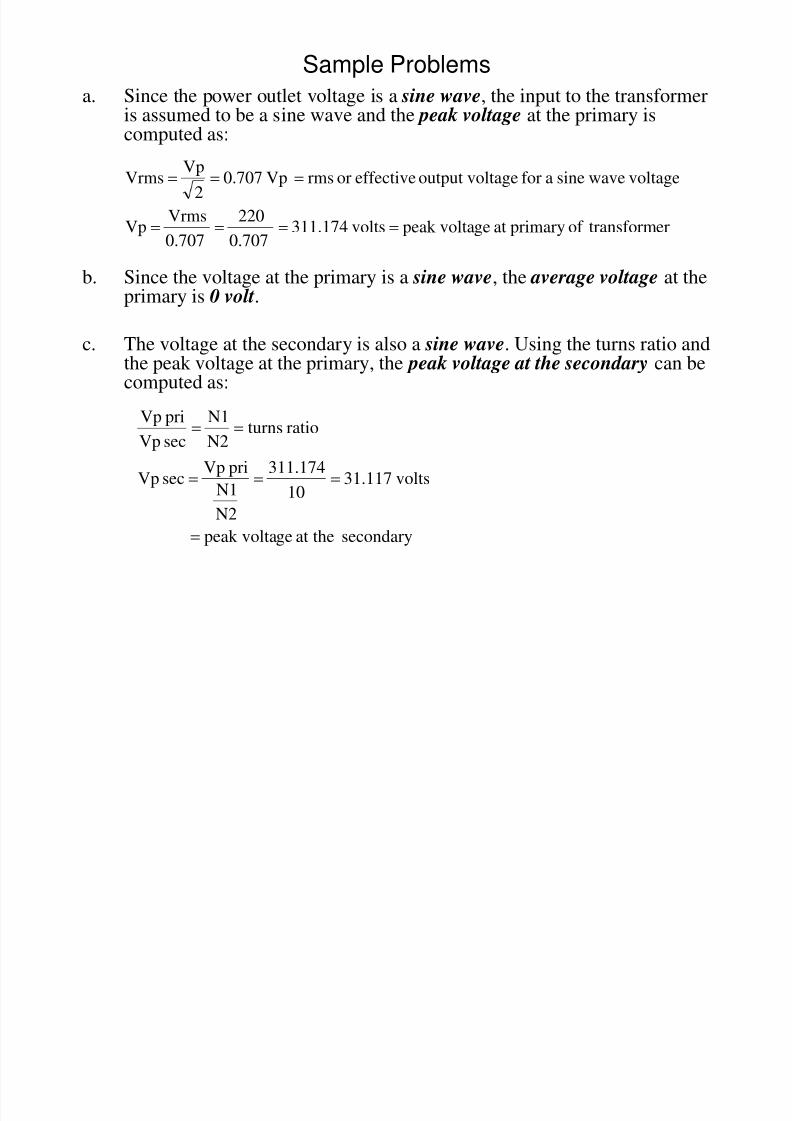
Sample Problems
• Example: A half wave rectifier uses a step down transformer. The input to
the primary of the transformer is 220 volts rms and the turns ratio of thetransformer (N1:N2) is 10:1. Load resistance (RL) is 5,000 ohms. Nocapacitor is connected at the output of the rectifier. Determine thefollowing:
a. Peak voltage at the primary
b. Average voltage at the primary
c. Peak voltage at the secondary
d. RMS voltage at the secondary
e. Average voltage at the secondary
f. Peak voltage at the output of the rectifier (across RL)
g. RMS voltage at the output of the rectifier (across RL)
h. Average voltage at the output of the rectifier (across RL)
i. Peak current at the load
j. RMS current at the load
k. Average current at the load
l. Minimum PIV of the diode (without capacitor filter)
S l P bl

8/7/2019 Electronics 1 Presentation Part 3 (ME)
http://slidepdf.com/reader/full/electronics-1-presentation-part-3-me 38/102
Sample Problems
a. Since the power outlet voltage is a sine wave, the input to the transformer
is assumed to be a sine wave and the peak voltage at the primary iscomputed as:
b. Since the voltage at the primary is a sine wave, the average voltage at theprimary is 0 volt.
c. The voltage at the secondary is also a sine wave. Using the turns ratio andthe peak voltage at the primary, the peak voltage at the secondary can becomputed as:
ertransformof primaryatgepeak voltavolts311.174 0.707
220
0.707
VrmsVp
voltagewavesineafortageoutput voleffectiveorrmsVp0.7072
VpVrms
secondaryat thegepeak volta
volts31.11710
311.174
N2
N1
priVpsecVp
ratioturnsN2
N1
secVp
priVp
S l P bl

8/7/2019 Electronics 1 Presentation Part 3 (ME)
http://slidepdf.com/reader/full/electronics-1-presentation-part-3-me 39/102
Sample Problems
d. As computed above, the rms voltage across the secondary is 22 volts.
e. Since the voltage at the secondary is also a sine wave, the average voltageat the secondary is 0 volt.
f. The peak voltage at the load (R L ) is approximately equal to the peakvoltage at the secondary which is 31.117 volts.
wave)(sinesecondaryatgepeak voltavolts31.117
707.0
22
0.707
secVrmssecVp
secondaryatvoltagermsvolts2210
220
N2
N1priVrms
secVrms
ratioturnsN2
N1
secVrms
priVrms
:followsassecondaryat thevoltagermsthe
computingfirstbycomputedbealsocansecondaryat thegepeak voltaThe
S l P bl

8/7/2019 Electronics 1 Presentation Part 3 (ME)
http://slidepdf.com/reader/full/electronics-1-presentation-part-3-me 40/102
Sample Problems
g. The rms voltage at the load is not the same as the rms voltage at the
secondary of the transformer and it can be computed as:
h. The average voltage at the load is not the same as the average voltage atthe secondary of the transformer and it can be computed as:
i. The peak current at the load can be computed as:
volts15.558)0.5(31.117secVp0.5Vp0.5RacrossVrms
rectifierwavehalf of tageoutput voleffectiveorrmsVp0.52
VpVrms
RLL
rectifierwavehalf of tageoutput volaveragevolts9.895(31.117)318.0secVp
Vdc
rectifierwavehalf of tageoutput volaverageVp318.0secVp318.0VpVdc RL
L3
L
RLRL Rthroughpassingcurrentpeak A10x6.223
5000
117.31
R
Vp Ip
Sample Problems

8/7/2019 Electronics 1 Presentation Part 3 (ME)
http://slidepdf.com/reader/full/electronics-1-presentation-part-3-me 41/102
Sample Problems
j. The rms current at the load can be computed as:
k. The average current at the load can be computed as:
l. The minimum PIV of the diode (without capacitor) is equal to the peak voltage of the secondary, which is 31.117 volts.
L3
L
RLRL RthroughpassingcurrentrmsA10x112.3
5000
558.15
R
Vrms Irms
L3
L
RLRL RthroughpassingcurrentaverageA10x979.1
5000
895.9
R
Vdc Idc
Rectifiers

8/7/2019 Electronics 1 Presentation Part 3 (ME)
http://slidepdf.com/reader/full/electronics-1-presentation-part-3-me 42/102
Rectifiers
• Example: A full wave rectifier is using a center tapped step down transformer.
The input to the primary of the transformer is 220 volts rms and the turns ratio of the transformer (N1:N2) is 10:1. Load resistance (RL) is 5,000 ohms. No capacitoris connected at the output of the rectifier. Determine the following: (Similar toprevious example except full wave rectifier with center tapped transformer)
a. Peak voltage at the primary
b. Average voltage at the primary
c. Peak voltage at the whole secondary and peak voltage at ½ of secondary
d. RMS voltage at the whole secondary and rms voltage at ½ of secondary
e. Average voltage at the whole secondary and average voltage at ½ of secondary
f. Peak voltage at the output of the rectifier (across RL)
g. RMS voltage at the output of the rectifier (across RL)
h. Average voltage at the output of the rectifier (across RL)
i. Peak current at the load
j. RMS current at the load
k. Average current at the load
l. Minimum PIV of the diode without capacitor
Sample Problems

8/7/2019 Electronics 1 Presentation Part 3 (ME)
http://slidepdf.com/reader/full/electronics-1-presentation-part-3-me 43/102
Sample Problems
a. Since the power outlet voltage is a sine wave, the input to the transformer
is assumed to be a sine wave and the peak voltage at the primary iscomputed as:
b. Since the voltage at the primary is a sine wave, the average voltage at theprimary is 0 volt.
c. The voltage at the secondary is also a sine wave. Using the turns ratio andthe peak voltage at the primary, the peak voltage at the whole secondarycan be computed as:
ertransformof primaryatgepeak voltavolts311.174 0.707
220 0.707
VrmsVp
voltagewavesineafortageoutput voleffectiveorrmsVp0.7072
VpVrms
secondarywholeat thegepeak volta
volts31.11710
311.174
N2
N1
priVpsecVp
ratioturnsN2
N1
secVp
priVp
Sample Problems

8/7/2019 Electronics 1 Presentation Part 3 (ME)
http://slidepdf.com/reader/full/electronics-1-presentation-part-3-me 44/102
Sample Problems
secondaryof 1/2atgepeak voltavolts15.5582
31.117
2
secVp Vp
wave)(sinesecondaryat wholegepeak voltavolts31.117707.0
22
0.707
secVrmssecVp
secondaryat wholevoltagermsvolts2210
220
N2
N1
priVrmssecVrms
ratioturnsN2
N1
secVrms
priVrms
:followsassecondaryat thevoltagermsthe
computingfirstbycomputedbealsocansecondaryat thegepeak voltaThe
sec1/2
d. As computed above, the rms voltage across the whole secondary is 22
volts. The rms voltage at ½ of secondary is one half the rms voltage of thewhole secondary and is equal to 22 / 2 = 11 volts.
e. Since the voltage at the secondary is also a sine wave, the average voltage at the whole secondary is 0 volt, and the average voltage at ½ of the
secondary is also equal to 0 volt.
Sample Problems

8/7/2019 Electronics 1 Presentation Part 3 (ME)
http://slidepdf.com/reader/full/electronics-1-presentation-part-3-me 45/102
Sample Problems
f. Since the peak voltage that appears across the load (R L ) is approximately
equal to the peak voltage at one half of the secondary, the peak voltage at the load (R L ) is approximately equal to the peak voltage at ½ of the secondary and it is equal to 31.117 / 2 = 15.558 volts.
g. The rms voltage at the output of rectifier or at the load can be computed as:
h. The average voltage at the output of the rectifier or at the load can becomputed as:
ertransformcenter tapusingrectifierwavefullof tageoutput voleffectiveorrms
volts11)558.15(707.0Vp0.7072
VpVrms
1/2sec1/2sec
rtransfomecenter tapusingrectifierwavefullof tageoutput volaverage
volts9.895)558.15)(636.0(Vp636.02VpVdc
sec1/2sec1/2
S l P bl

8/7/2019 Electronics 1 Presentation Part 3 (ME)
http://slidepdf.com/reader/full/electronics-1-presentation-part-3-me 46/102
Sample Problemsi. The peak current at the load can be computed as:
j. The rms current at the load can be computed as:
k. The average current at the load can be computed as:
l. The minimum PIV of the diode (without capacitor) is equal to the peakvoltage of the whole secondary, which is 31.117 volts.
L3
L
RLRL RthroughpassingcurrentaverageA10x979.1
5000
895.9
R
Vdc Idc
L3
L
RLRL RthroughpassingcurrentrmsA10x2.2
5000
11
R
Vrms Irms
L3
L
RLRL Rthroughpassingcurrentpeak A10x112.3
5000
558.15
R
Vp Ip
Rectifiers

8/7/2019 Electronics 1 Presentation Part 3 (ME)
http://slidepdf.com/reader/full/electronics-1-presentation-part-3-me 47/102
Rectifiers
• Example: A full wave bridge rectifier is using a step down transformer. The input
to the primary of the transformer is 220 volts rms and the turns ratio of thetransformer (N1:N2) is 10:1. Load resistance (RL) is 5,000 ohms. No capacitor isconnected at the output of the rectifier. Determine the following: (Similar toprevious two examples except full wave bridge rectifier)
a. Peak voltage at the primary
b. Average voltage at the primary
c. Peak voltage at the secondary
d. RMS voltage at the secondary
e. Average voltage at the secondary
f. Peak voltage at the output of the rectifier (across RL)
g. RMS voltage at the output of the rectifier (across RL)
h. Average voltage at the output of the rectifier (across RL)
i. Peak current at the load
j. RMS current at the load
k. Average current at the load
l. Minimum PIV of the diode without capacitor
Sample Problems
8/7/2019 Electronics 1 Presentation Part 3 (ME)
http://slidepdf.com/reader/full/electronics-1-presentation-part-3-me 48/102
Sample Problems
a. Since the power outlet voltage is a sine wave, the input to the transformer
is assumed to be a sine wave and the peak voltage at the primary iscomputed as:
b. Since the voltage at the primary is a sine wave, the average voltage at theprimary is 0 volt.
c. The voltage at the secondary is also a sine wave. Using the turns ratio andthe peak voltage at the primary, the peak voltage at the secondary can becomputed as:
ertransformof primaryatgepeak voltavolts311.174 0.707
220
0.707
VrmsVp
voltagewavesineafortageoutput voleffectiveorrmsVp0.7072
VpVrms
secondary at thegepeak volta
volts31.11710
311.174
N2
N1
priVpsecVp
ratioturnsN2
N1
secVp
priVp
Sample Problems

8/7/2019 Electronics 1 Presentation Part 3 (ME)
http://slidepdf.com/reader/full/electronics-1-presentation-part-3-me 49/102
Sample Problems
wave)(sinesecondaryat wholegepeak voltavolts31.117
707.0
22
0.707
secVrmssecVp
secondaryat wholevoltagermsvolts2210
220
N2
N1
priVrmssecVrms
ratioturnsN2
N1
secVrms
priVrms
:followsassecondaryat thevoltagermsthe
computingfirstbycomputedbealsocansecondaryat thegepeak voltaThe
d. As computed above, the rms voltage across the whole secondary is 22volts.
e. Since the voltage at the secondary is also a sine wave, the average voltage at the secondary is 0 volt.
Sample Problems

8/7/2019 Electronics 1 Presentation Part 3 (ME)
http://slidepdf.com/reader/full/electronics-1-presentation-part-3-me 50/102
p
f. The peak voltage that appears across the load (R L ) is approximately equal to
the peak voltage at the secondary and it is equal to 31.117 volts.
g. The rms voltage at the output of rectifier or at the load can be computed as:
h. The average voltage at the output of the rectifier or at the load can becomputed as:
rectifierbridgewavefullof tageoutput voleffectiveorrms
volts22)117.31(707.0secVp0.7072secVpVrms
rectifierbridgewavefullof tageoutput volaverage
volts79.91)117.31)(636.0(secVp636.0sec2Vp
Vdc
Sample Problems

8/7/2019 Electronics 1 Presentation Part 3 (ME)
http://slidepdf.com/reader/full/electronics-1-presentation-part-3-me 51/102
Sample Problemsi. The peak current at the load can be computed as:
j. The rms current at the load can be computed as:
k. The average current at the load can be computed as:
l. The minimum PIV of the diode (without capacitor) is equal to the peakvoltage of the whole secondary, which is 31.117 volts.
L3
L
RLRL RthroughpassingcurrentaverageA10x958.3
5000
79.19
R
Vdc Idc
L3
L
RLRL RthroughpassingcurrentrmsA10x4.4
5000
22
R
Vrms Irms
L3
L
RLRL Rthroughpassingcurrentpeak A10x223.6
5000
117.31
R
Vp Ip
Sample Problems

8/7/2019 Electronics 1 Presentation Part 3 (ME)
http://slidepdf.com/reader/full/electronics-1-presentation-part-3-me 52/102
p
• Example: The average (dc) current at the load of a half wave rectifier is
50 mA and the load resistance is 4,000 ohms. Determine:a. Average output voltage of the rectifier (or across the load)
b. Peak voltage at the output of the rectifier (or across the load)
c. RMS output voltage of the rectifier (or across the load)
d. Minimum PIV rating of the diode
rectifierof outputorloadatgepeak voltavolts628.93318.0
200
0.318
Vdc Vp
loadatvoltageaverageVp0.318Vdc
rectifierof tageoutput volaverageloadatvoltageaverage
volts200)000,4)(10x0(5 )(RIdcVdc
rectifierof outputatcurrentaverageRthroughpassingcurrentaverage
A10x05R
Vdc Idc
RL RL
RLRL
3LRLRL
L
3
L
RLRL
Sample Problems

8/7/2019 Electronics 1 Presentation Part 3 (ME)
http://slidepdf.com/reader/full/electronics-1-presentation-part-3-me 53/102
)(Rloadat thevoltageeffectiveorrms
rectifierwavehalf of tageoutput voleffectiveorrms
volts314.4652
628.93
2
VpVrms
L
RL
The minimum PIV of the diode (without capacitor) is equal to the peak voltage
of the secondary or load, which is 628.93 volts.
Rectifiers

8/7/2019 Electronics 1 Presentation Part 3 (ME)
http://slidepdf.com/reader/full/electronics-1-presentation-part-3-me 54/102
• Example:
Rectifiers

8/7/2019 Electronics 1 Presentation Part 3 (ME)
http://slidepdf.com/reader/full/electronics-1-presentation-part-3-me 55/102
• Example:
Rectifiers

8/7/2019 Electronics 1 Presentation Part 3 (ME)
http://slidepdf.com/reader/full/electronics-1-presentation-part-3-me 56/102
• Example:

8/7/2019 Electronics 1 Presentation Part 3 (ME)
http://slidepdf.com/reader/full/electronics-1-presentation-part-3-me 57/102
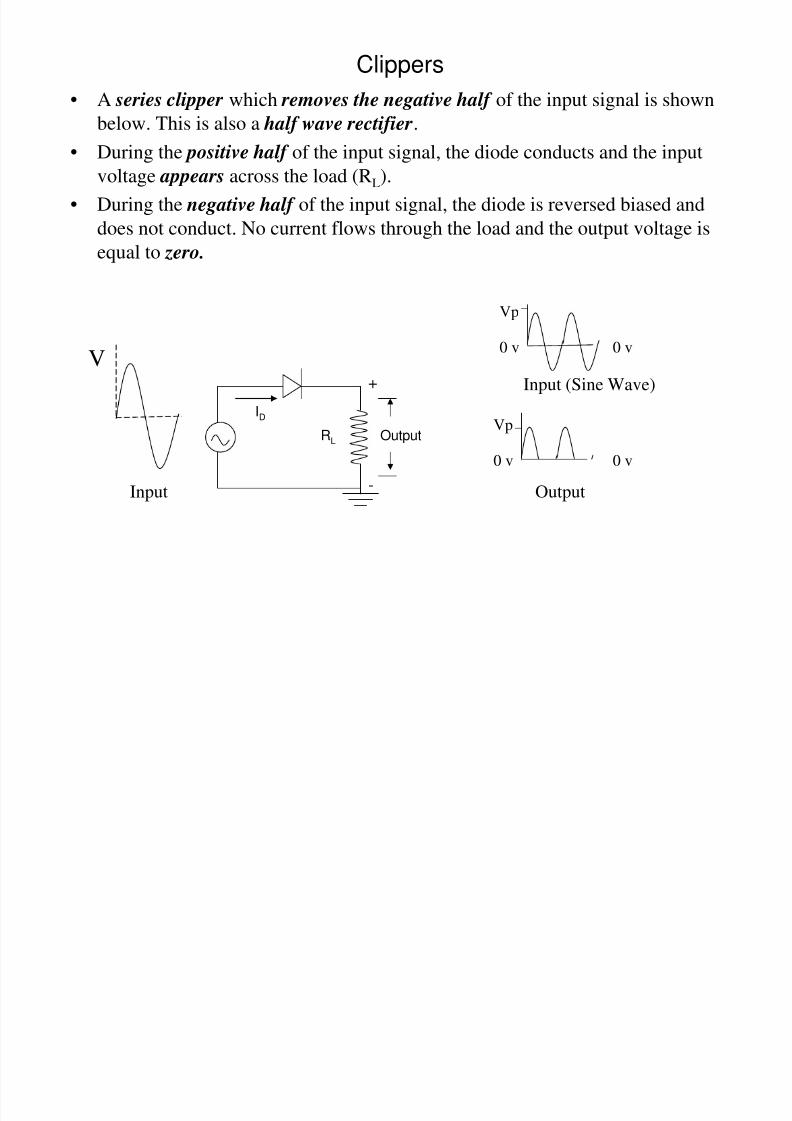
Clippers
Prepared by: Armando V. Barretto
Clippers

8/7/2019 Electronics 1 Presentation Part 3 (ME)
http://slidepdf.com/reader/full/electronics-1-presentation-part-3-me 58/102
• Clippers are networks which are used to remove or “clip” away a portion of
the input signal without distorting the remaining part of the input signal.• The input signal could be a square wave, sine wave or any other waveform.
• A half wave rectifier is a clipper which removes half of the input signal.
• The two general categories of clippers are series clipper and parallel clipper.
• A series clipper is one where the diode is in series with the load .• A parallel clipper is one where the diode is in a branch parallel with the load .
• The considerations in analyzing clippers are:
– Take careful note of where the output voltage is.
– Analyze which diodes are forward biased and which are reverse biased under certain conditions.
– Forward biased diodes may be considered short circuits while reverse biased diodes may be considered open circuits.
– DC voltages from batteries will add or subtract from the input signal and
the resulting voltages will determine the biasing of the diodes.• If the voltage drops across the diodes are considered , the voltage drops across
the conducting diodes must be subtracted from the peak voltages in theequations.
Clippers
8/7/2019 Electronics 1 Presentation Part 3 (ME)
http://slidepdf.com/reader/full/electronics-1-presentation-part-3-me 59/102
• A series clipper which removes the negative half of the input signal is shown
below. This is also a half wave rectifier.
• During the positive half of the input signal, the diode conducts and the input
voltage appears across the load (RL).
• During the negative half of the input signal, the diode is reversed biased and
does not conduct. No current flows through the load and the output voltage isequal to zero.
ID
RL Output
Input (Sine Wave)
Output
Vp
Vp
V
Input
+
-
0 v
0 v
0 v
0 v
Clippers

8/7/2019 Electronics 1 Presentation Part 3 (ME)
http://slidepdf.com/reader/full/electronics-1-presentation-part-3-me 60/102
• A series clipper which removes the positive half of the input signal is shown
below. This is also a half wave rectifier.• During the negative half of the input signal, the diode conducts and the input
voltage appears across the load (RL).
• During the positive half of the input signal, the diode is reversed biased and
does not conduct. No current flows through the load and the output voltage isequal to zero.
ID RL Output
Input (Sine Wave)
Output-Vp
Vp
V
Input
0 v
0 v0 v
0 v
Clippers

8/7/2019 Electronics 1 Presentation Part 3 (ME)
http://slidepdf.com/reader/full/electronics-1-presentation-part-3-me 61/102
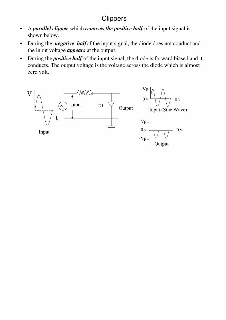
• A parallel clipper which removes the negative half of the input signal is
shown below.• During the positive half of the input signal, the diode does not conduct and
the input voltage appears at the output.
• During the negative half of the input signal, the diode is forward biased and it
conducts. The output voltage is the voltage across the diode which is almostzero volt.
OutputInput D1
t
V
Input
Input (Sine Wave)
Output
Vp
Vp
0 v
0 v0 v
0 v
Clippers
ll l l h h lf
8/7/2019 Electronics 1 Presentation Part 3 (ME)
http://slidepdf.com/reader/full/electronics-1-presentation-part-3-me 62/102
• A parallel clipper which removes the positive half of the input signal is
shown below.• During the negative half of the input signal, the diode does not conduct and
the input voltage appears at the output.
• During the positive half of the input signal, the diode is forward biased and it
conducts. The output voltage is the voltage across the diode which is almostzero volt.
OutputInput D1
t
V
Input
Vp
Input (Sine Wave)
Output-Vp
Vp
0 v
0 v0 v
0 v
Clippers• A biased series clipper which removes a portion of the negative half of the input

8/7/2019 Electronics 1 Presentation Part 3 (ME)
http://slidepdf.com/reader/full/electronics-1-presentation-part-3-me 63/102
• A biased series clipper which removes a portion of the negative half of the input
signal is shown below.• When the input signal is 0 volt, the diode is forward biased because of the 3 volt
battery. The diode conducts and approximately 3 volts appear at the output.
• During the positive half of the input signal, the input voltage adds up with the 3
volt battery and the diode is forward biased . The diode conducts and the sum of the input voltage and 3 volt battery appears at the output.
• During the negative half of the input signal, the diode remains forward biased
because of the 3 volt battery until the input voltage becomes approximately equal
to 3 volts. When the negative half of the input signal becomes approximately -3
volts or more negative, the diode is reversed biased and does not conduct. No
current flows through the resistor and the output voltage is equal to zero.
ID R Output
Input (Sine Wave)
t
10 v
Vp=10 v
Vp=10 v
Input
V= 3 volts
3 v
13 v
Output
Vp + V =10+3v
+
- 0 v
0 v0 v
Clippers• A biased series clipper which removes the negative half of the input signal and a

8/7/2019 Electronics 1 Presentation Part 3 (ME)
http://slidepdf.com/reader/full/electronics-1-presentation-part-3-me 64/102
• A biased series clipper which removes the negative half of the input signal and a
portion of the positive half of the input signal is shown below.• When the input signal is 0 volt, the diode is reverse biased because of the 3 volt
battery. The diode does not conduct and output voltage is equal to zero.
• During the positive half of the input signal, the diode remains reverse biased
because of the 3 volt battery until the input voltage becomes approximately equalto + 3 volts. When the positive half of the input signal becomes more positive than
approximately 3 volts, the diode is forward biased and it conducts. Current flows
through the resistor and output voltage becomes greater than 0 volt. Peak voltage
is approximately equal to the peak voltage of input minus 3 volts (7 volts).
• During the negative half of the input signal, the diode is reverse biased . There is
no current and output is equal to 0 volt.
ID R Output
Input (Sine Wave)
t
7 v
Vp=10 v
Vp=10 v
Input
V=3 volts
3 v
Output
Vp-V = 10 v-3v
+
-0 v
0 v0 v
Clippers• A biased series clipper which removes a portion of the positive half of the input

8/7/2019 Electronics 1 Presentation Part 3 (ME)
http://slidepdf.com/reader/full/electronics-1-presentation-part-3-me 65/102
A biased series clipper which removes a portion of the positive half of the input
signal is shown below.• When the input signal is 0 volt, the diode is forward biased because of the - 3 volt
battery. The diode conducts and approximately - 3 volts appear at the output.
• During the positive half of the input signal, the diode remains forward biased
because of the - 3 volt battery until the input voltage becomes greater than approximately + 3 volts. When the positive half of the input signal becomes greater
than approximately + 3 volts, the diode is reversed biased and does not conduct. No
current flows through the resistor and the output voltage is equal to zero.
• During the negative half of the input signal, the input voltage adds up with the - 3
volt battery and the diode is forward biased . The diode conducts and the sum of the
input voltage and -3 volt battery appears at the output.
ID R Output
Input (Sine Wave)
Vp=10 v
Vp=10 v
Input
V= 3 volts
-3 v
-13 v Output -Vp-V= -10-3v
0 v
0 v0 v
0 v
Clippers• A biased series clipper which removes the positive half and a portion of the

8/7/2019 Electronics 1 Presentation Part 3 (ME)
http://slidepdf.com/reader/full/electronics-1-presentation-part-3-me 66/102
A biased series clipper which removes the positive half and a portion of the
negative half of the input signal is shown below.• When the input signal is 0 volt, the diode is reverse biased because of the 3 volt
battery. The diode does not conduct and output is equal to zero volt..
• During the positive half of the input signal, the input signal adds to the voltage of
the battery, the diode remains reverse biased and does not conduct. No currentflows through the resistor and the output voltage is equal to zero.
• During the negative half of the input signal, the diode remains reverse biased until
the input signal becomes more negative than approximately – 3 volts. When the
input signal becomes more negative than approximately – 3 volts, the diode
conducts, current flows through the resistor, and negative output voltage appears
at the output.
ID R Output
Input (Sine Wave)
Vp=10 v
Vp=10 v
Input
V= 3 volts
-7 v Output-Vp + V= -10 + 3v
0 v
0 v
0 v
0 v
Clippers• A biased parallel clipper which removes a portion of the positive half of the input
i l i h b l

8/7/2019 Electronics 1 Presentation Part 3 (ME)
http://slidepdf.com/reader/full/electronics-1-presentation-part-3-me 67/102
signal is shown below.
• When the input signal is 0 volt, the diode is reverse biased . The diode does not
conduct and output voltage is equal to zero.
• During the positive half of the input signal, the diode remains reverse biased
because of the 3 volt battery until the input voltage becomes more positive than
approximately 3 volts. When the positive half of the input signal becomes more positive than approximately 3 volts, the diode is forward biased and it conducts.
Output voltage becomes equal to 3 volts because the diode is effectively a short
circuit when it conducts.
• During the negative half of the input signal, input signal adds up with the batteryvoltage, the diode is reverse biased and output voltage is equal to the input signal.
Input (Sine Wave)
Vp=10 v
3 v
Output
OutputInputV = 3 v
Vp=10 v
Input
Vp=10 v
-Vp = -10v
0 v
0 v0 v
0 vV = 3 v
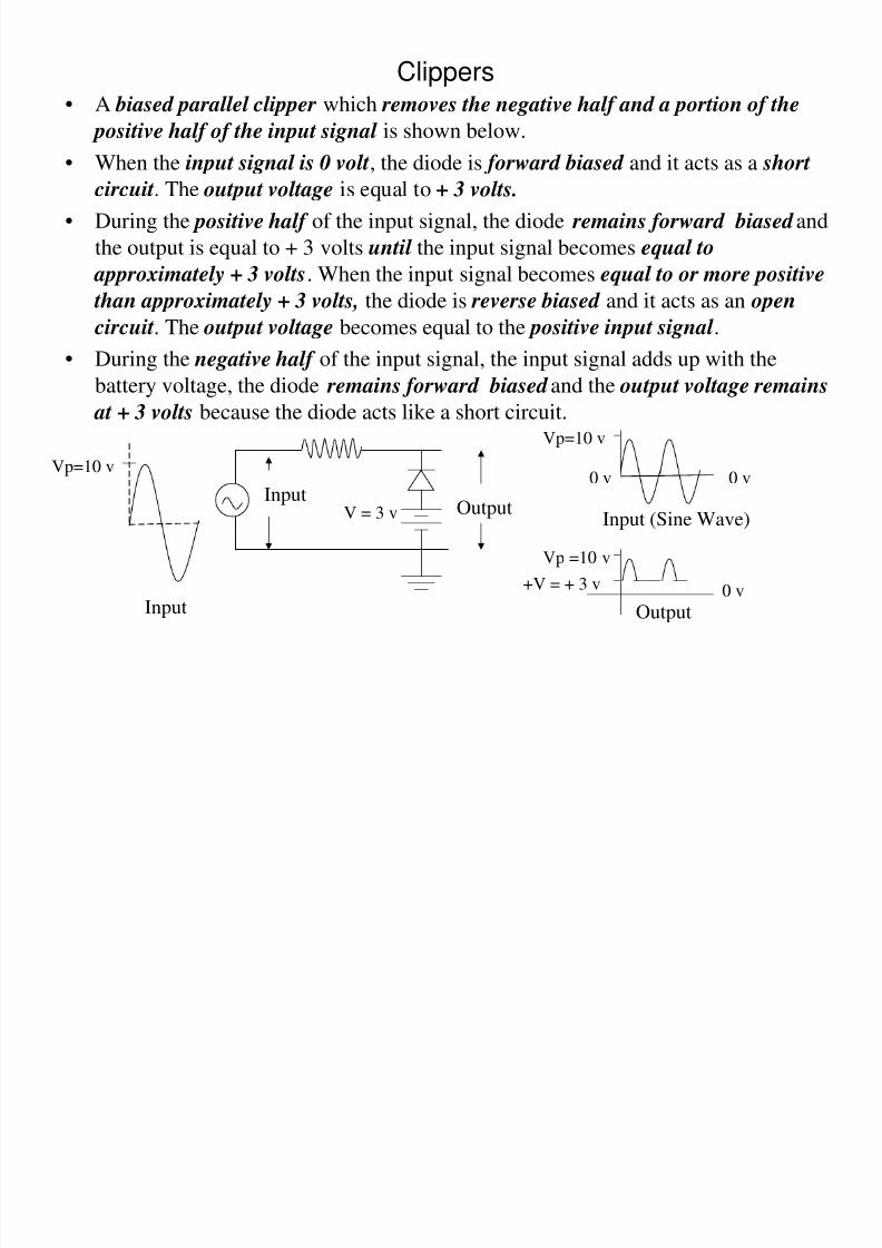
Clippers• A biased parallel clipper which removes the positive half of the input signal and

8/7/2019 Electronics 1 Presentation Part 3 (ME)
http://slidepdf.com/reader/full/electronics-1-presentation-part-3-me 68/102
p pp p f f p g
a portion of the negative half of the input signal is shown below.• When the input signal is 0 volt, the diode is forward biased and it acts as a short
circuit. The output voltage is equal to – 3 volts.
• During the positive half of the input signal, the diode remains forward biased and
the output voltage remains at – 3 volts because the diode acts like a short circuit.• During the negative half of the input signal, the diode remains forward biased
until the input signal becomes equal to approximately – 3 volts. When the input
signal becomes equal to or more negative than approximately – 3 volts, the diode
is reverse biased and it acts as an open circuit. The output voltage becomes equal
to the negative input signal.
Input (Sine Wave)
Vp=10 v
-V= -3 v
Output
OutputInputV = 3 v
Vp=10 v
Input
Vp=10 v
-Vp = -10 v
0 v
0 v0 v
0 v
Clippers• A biased parallel clipper which removes a portion of the negative half of the

8/7/2019 Electronics 1 Presentation Part 3 (ME)
http://slidepdf.com/reader/full/electronics-1-presentation-part-3-me 69/102
p pp p f g f f
input signal is shown below.• When the input signal is 0 volt, the diode is reverse biased . The diode acts like an
open circuit and output voltage is equal to zero.
• During the positive half of the input signal, the input signal adds up with the
battery voltage, the diode remains reverse biased and acts like an open circuit.The output voltage is equal to the positive input voltage.
• During the negative half of the input signal, the diode remains reverse biased and
acts like an open circuit until the input signal becomes more negative than
approximately -3 volts. When the input signal becomes more negative than
approximately -3 volts, the diode is forward biased and it acts like a short circuit.
The output becomes equal to – 3 volts.
Input (Sine Wave)
Vp=10 v
OutputInputV = 3 v
Vp=10 v
Input
0 v
Vp =10 v
0 v
Output
-V = -3 v
0 v
Clippers• A biased parallel clipper which removes the negative half and a portion of the
8/7/2019 Electronics 1 Presentation Part 3 (ME)
http://slidepdf.com/reader/full/electronics-1-presentation-part-3-me 70/102
positive half of the input signal is shown below.• When the input signal is 0 volt, the diode is forward biased and it acts as a short
circuit. The output voltage is equal to + 3 volts.
• During the positive half of the input signal, the diode remains forward biased and
the output is equal to + 3 volts until the input signal becomes equal to approximately + 3 volts. When the input signal becomes equal to or more positive
than approximately + 3 volts, the diode is reverse biased and it acts as an open
circuit. The output voltage becomes equal to the positive input signal .
• During the negative half of the input signal, the input signal adds up with the
battery voltage, the diode remains forward biased and the output voltage remains
at + 3 volts because the diode acts like a short circuit.
Input (Sine Wave)
Vp=10 v
+V = + 3 v
OutputInputV = 3 v
Vp=10 v
Input
0 v
0 v
Vp =10 v
Output
0 v
Clippers• A biased parallel clipper which removes a portion of the positive half and a
i f h i h lf f h i i l

8/7/2019 Electronics 1 Presentation Part 3 (ME)
http://slidepdf.com/reader/full/electronics-1-presentation-part-3-me 71/102
portion of the negative half of the input signal is shown below.
• When the input signal is 0 volt, the diodes are reverse biased and they act like open circuits. The output voltage is equal to zero volt.
• During the positive half of the input signal, D2 remains reverse biased all throughout while D1 remains reverse biased until the input signal becomes more positive
than approximately + 3 volts. When the input signal becomes more positive than approximately + 3 volts, D1 is forward biased and it acts like a short circuit. Theoutput voltage becomes equal to + 3 volts.
• During the negative half of the input signal, D1 remains reverse biased all throughout while D2 remains reverse biased until the input signal becomes more negative
than approximately - 3 volts. When the input signal becomes more negative than approximately - 3 volts, D2 is forward biased and it acts like a short circuit. Theoutput voltage becomes equal to - 3 volts.
Input (Sine Wave)
Vp=10 v
OutputInput D1
3 v3 v
D2
Vp=10 v
Input Output
Vp=10 v
+ 3 v
- 3 v
0 v
0 v

8/7/2019 Electronics 1 Presentation Part 3 (ME)
http://slidepdf.com/reader/full/electronics-1-presentation-part-3-me 72/102
Resistor – Capacitor (RC)Networks
Prepared by: Armando V. Barretto
RC Network
i

8/7/2019 Electronics 1 Presentation Part 3 (ME)
http://slidepdf.com/reader/full/electronics-1-presentation-part-3-me 73/102
E
(charging
voltage)
R
1 k
C
4 F
eR
eC
10 v
+
-
S1
iC
+
-
eC
(volt)
Time (t)
3
6
9
t1 t2 t3
E = supply voltage
eR = instantaneous voltage across resistor R
ec = instantaneous voltage across capacitor C
When S1 is closed, capacitor C will be charged towards the supply voltage
E. As the capacitor voltage increases, the charging current decreases.
Capacitor voltage
Charging current
RC Circuit Operation

8/7/2019 Electronics 1 Presentation Part 3 (ME)
http://slidepdf.com/reader/full/electronics-1-presentation-part-3-me 74/102
• The instantaneous voltage across resistor R iseR = E – ec
Where: eR = instantaneous voltage across the resistor R
E = supply voltage
ec = instantaneous voltage across the capacitor C
• The instantaneous current passing through R and C is
R
eEi
R
ei
CC
RC
RC Circuit Operation

8/7/2019 Electronics 1 Presentation Part 3 (ME)
http://slidepdf.com/reader/full/electronics-1-presentation-part-3-me 75/102
• If the charge on the capacitor C is zero at the instant that the switch isclosed, then at t = 0, the current passing through R and C is
• This current causes the capacitor C to charge with the polarity illustrated,
so that at time t1, the capacitor voltage eC could be 3 volts. This alters eR
eR = E – ec
= 10 v – 3 v = 7 v
• Because C has accumulated some charge, eC is increased and the voltage
across R is reduced; thus the charging current through R is also reduced.
10mAkohm1
0v10i
R
eEi
C
CC
RC Circuit Operation

8/7/2019 Electronics 1 Presentation Part 3 (ME)
http://slidepdf.com/reader/full/electronics-1-presentation-part-3-me 76/102
• Since the charging current is reduced , C is being charged at a lower ratethan before.
• After some longer time period, eC increases to 6 v., and the voltage across
R is
eR
= 10 v – 6 v = 4 v
• The charging current has now been reduced further, and even longer time period is required to charge C by another 3 volts.
• The capacitor does not receive its charge at a constant rate.
• When the voltage across C is increasing, the voltage across R is
decreasing, and the charging current is also decreasing.• C is charged at a rapid rate initially, and then the charging rate decreases
as the capacitor voltage increases.
mA4kohm1
v6v10iC
RC Circuit Operation

8/7/2019 Electronics 1 Presentation Part 3 (ME)
http://slidepdf.com/reader/full/electronics-1-presentation-part-3-me 77/102
• The capacitor voltage follows the exponential equation
(ohms)resistorof resistanceR
(Farad)capacitorof ecapacitancC
(seconds)chargeof ntcommencemefromtimet
2.718constantlexponentia
(volt)capacitoron thechargeinitialEo
(volt) voltagechargingE
(volt)instant tatRacrossvoltagee
(volt)instant tatvoltagecapacitore:Where
Eo)(Ee
is Rresistortheacross voltagetheand
Eo)(EEe
R
c
RC
t -
R
RC
t -
c
RC Circuit Operation
When there is no initial voltage on the capacitor,

8/7/2019 Electronics 1 Presentation Part 3 (ME)
http://slidepdf.com/reader/full/electronics-1-presentation-part-3-me 78/102
charged.iscapacitortheassmallerandsmallerbecomescurrentchargingtheas
tage,supply volthetochargedfullybecomeneverwillcapacitorThe
current)charging(initial R
EI:Where
Ii
R
Ei
R
)-E(1-Ei
R
e-Ei
iscapacitorandresistorhethrough tflowingcurrentousinstantaneThe
)-E(1e
capacitor)theof voltageeous(instantan 0)(EEe
capacitor)theof voltage(initial 0Eo
RC
RC
RC
C
RC
RC
t-
C
t-
C
t-
C
C
t-
c
t-
c
RC Circuit Operation
• When the capacitor becomes charged to a certain voltage Eo, and is

8/7/2019 Electronics 1 Presentation Part 3 (ME)
http://slidepdf.com/reader/full/electronics-1-presentation-part-3-me 79/102
p g g ,
discharged through a resistor R (without a supply voltage), the following
equation can also be used to compute for the capacitor voltage at any time
during discharge:
(ohms)resistorof resistanceR
(Farad)capacitorof ecapacitancC
(seconds)dischargeof ntcommencemefromtimet
2.718constantlexponentia
(volt)capacitoron thechargeinitialEo
volt0(volt) voltagechargingE
(volt)instant tatvoltagecapacitore:Where
Eoe
Eo)(00e
Eo)(EEe
c
RC
t -
c
RC
t -
c
RC
t -
c
RC Circuit Operation
• Example: A 1 F capacitor is charged from a 6 v source through a 10

8/7/2019 Electronics 1 Presentation Part 3 (ME)
http://slidepdf.com/reader/full/electronics-1-presentation-part-3-me 80/102
Example: A 1 F capacitor is charged from a 6 v source through a 10kohm resistor. If the capacitor has an initial voltage of – 3 volts,calculate its voltage after 8 ms.
Solution:
volts1.96e
3v))(v(6v6e
Eo)(EEe
c
k)(1uF)(10
ms8 -
c
RC
t-
c
RC Time Constant
Capacitor
voltageCapacitor Charging voltage (E)

8/7/2019 Electronics 1 Presentation Part 3 (ME)
http://slidepdf.com/reader/full/electronics-1-presentation-part-3-me 81/102
eC
(volt)
time (t) in ms
4 v
6 v
8 v
4 ms2 ms 6 ms
vo tage
E =10 v
2 v
12 ms10 ms8 ms 14 ms 16 ms 18 ms 20 ms
90 % E99.3 % E
(at t = 5 RC)
63.2 % E
(at t = RC)
Initial Chargingcurrent voltage whilecharging
Regardless of the value of E, R and C, the capacitor is charged to 63.2 % E
when t = RC, to 90 % E at t = 2.2 RC, and to 99.3 % E at t = 5 RC.
In the diagram, it was assumed that E = 10 volts, R = 1 kohm, and C = 4 F.
Thus RC = 4 ms
(10 volts)
RC Time Constant

8/7/2019 Electronics 1 Presentation Part 3 (ME)
http://slidepdf.com/reader/full/electronics-1-presentation-part-3-me 82/102
• The product RC is the time constant of the RC circuit. It is the time whenthe capacitor is charged to 63.2 % E, regardless of the value of E, R, and C.(assuming initial charge of C is zero)
• At time 5 RC , the capacitor is charged to 99.3 % E, regardless of the valueof E, R, and C. (assuming initial charge of C is zero).
• For practical purposes, it is assumed that the capacitor is fully charged or discharged at t = 5 RC .
• At t = RC, the current flowing through R and C is 36.8 % I . Where I is theinitial charging current which is equal to E / R.
• When a capacitor is charged from a DC voltage source through a resistor,the instantaneous level of the capacitor voltage may be calculated at anygiven time.
• There is a definite relationship between the time constant of the RCnetwork and the time required for the capacitor to charge to approximately
63 % and 99 % of the input voltage.
RC Time Constant
SquareV

8/7/2019 Electronics 1 Presentation Part 3 (ME)
http://slidepdf.com/reader/full/electronics-1-presentation-part-3-me 83/102
Input
voltage
R
C
eR
eC
10 v
S1
iC when Cis charging
Output
(across resistor)
vi
wave
input
t
t
t
eR
for
RC= 10 PW
eR
for
RC=PW
eR
for
RC= PW / 10
t
PW
eR
eR
eR
During the time that input voltage is positive, C is
charged towards the peak voltage of the input signal.
The output voltage across R is equal to the inputvoltage minus the voltage across the capacitor. When
the input signal becomes 0 v, the capacitor discharges
through R , during which the current is in the reverse
direction, causing a negative going pulse across R.
iC when Cis discharging
V1 V2
V3 V4
V1
V2
V3 V4
V1
V2
V3
V4

8/7/2019 Electronics 1 Presentation Part 3 (ME)
http://slidepdf.com/reader/full/electronics-1-presentation-part-3-me 84/102
Clampers
Prepared by: Armando V. Barretto
Clampers
• Clampers are networks which shifts a waveform to a different dc level without

8/7/2019 Electronics 1 Presentation Part 3 (ME)
http://slidepdf.com/reader/full/electronics-1-presentation-part-3-me 85/102
changing the appearance of the waveform.• Clampers are typically constructed using diodes, capacitors and resistors.
• The dc shifts are typically provided by the capacitor which charges up to acertain dc voltage when the diode is conducting.
• Additional dc shifts can be introduced in a clamper network by using dc supplies.
• When the capacitor is charging, the resistor is typically shorted out and the RCtime constant is effectively 0 sec. The capacitor is charged instantaneously to theapplied voltage because the RC time constant is 0.
• When the capacitor is discharging, the resistor is not shorted out and the RC time constant of the resistor and capacitor combination must be high enough so
that the voltage drop across the capacitor is not significant while it is discharging.
– It is desired that the RC time constant is much greater than 5 times the discharging time of the capacitor (time when diode is not conducting).
– In the analysis of clampers, it is assumed that the voltage drop across the
capacitor while it is discharging is negligible.• The input signal could be a square wave, sine wave or any other periodical
waveform.
Clampers• The considerations in analyzing clippers are:
– Begin the analysis by taking note of which portion of the input signal is the

8/7/2019 Electronics 1 Presentation Part 3 (ME)
http://slidepdf.com/reader/full/electronics-1-presentation-part-3-me 86/102
diode forward biased and the capacitor charged to a certain dc level.
– Assume that the capacitor is charged up instantaneously to the appliedvoltage when the diode is “on”. Typically, the resistor is shorted out whenthe diode is conducting and the capacitor is fully charged instantaneously to
the applied voltage because the RC time constant is effectively 0 second when the capacitor is charging.
– With the capacitor is charged, it is like a battery whose voltage will add to or subtract from the input signal.
– Determine the output signal while assuming that the capacitor is fully
charged when the diode is not conducting. It is assumed that the RC time constant when the capacitor is discharging is high enough that the voltageacross the capacitor does not drop significantly.
– Check if the shape of the output waveform is the same as that of the inputsignal except for the change in the dc level in the output waveform.
• In the succeeding analysis, approximate approach is used and it is assumed that a diode is shorted when forward biased and voltage across the diode is 0 v.
• When considering the voltage across the diode (when it is forward biased) isdesired, simply replace the diode with a battery with the corresponding forward
biased voltage ( 0.7 for Si, 0.3 for Ge).
Clampers• A Clamper which shifts the dc level from 0 volt to the negative peak voltage
(-Vp) of the input signal is shown below.

8/7/2019 Electronics 1 Presentation Part 3 (ME)
http://slidepdf.com/reader/full/electronics-1-presentation-part-3-me 87/102
• During the positive half of the input signal, the diode conducts, the capacitoris charged to the peak voltage (Vp) of the input signal with the polarityshown, and the output voltage is approximately equal to zero volt becausethe diode acts almost like a short circuit. The capacitor chargesinstantaneously to the peak voltage of the input signal because the resistor iseffectively shorted out (RC time constant = 0).
• During the negative half of the input signal, the input signal which is –Vp adds up to the voltage across the capacitor, the diode is reverse biased and itacts like an open circuit. The output voltage becomes equal to two times the
negative of the peak voltage (-2Vp) of the input signal (voltage acrosscapacitor plus input voltage).
OutputInput D1
Square
wave
input
0 v
PW
Output
PW
+ -Vp
0 v
Vp
-2Vp
-Vp DC = 0 v
DC = -Vp-Vp
T
0 v
0 v
Clampers• A Clamper which shifts the dc level from 0 volt to the positive peak voltage
(+Vp) of the input signal is shown below.
i h lf di d d

8/7/2019 Electronics 1 Presentation Part 3 (ME)
http://slidepdf.com/reader/full/electronics-1-presentation-part-3-me 88/102
• During the negative half of the input signal, the diode conducts, the capacitoris charged to the peak voltage (Vp) of the input signal with the polarityshown, and the output voltage is approximately equal to zero volt becausethe diode acts almost like a short circuit. The capacitor chargesinstantaneously to the peak voltage of the input signal because the resistor iseffectively shorted out (RC time constant = 0).
• During the positive half of the input signal, the input signal which is +Vp adds up to the voltage across the capacitor, the diode is reverse biased and itacts like an open circuit. The output voltage becomes equal to two times the
peak voltage (2Vp) of the input signal (voltage across capacitor plus inputvoltage).
OutputInputD1
Square
wave
input
0 v
PW
OutputPW
+-Vp
0 v
Vp
2Vp
-Vp DC = 0 v
DC = +VpVp
T
0 v
0 v
Clampers• A Clamper using a dc supply, which shifts the dc level from -2.5 v to + 10.5 v, is
shown below.
D i h i i f h i i l h i i l dd i h h

8/7/2019 Electronics 1 Presentation Part 3 (ME)
http://slidepdf.com/reader/full/electronics-1-presentation-part-3-me 89/102
• During the negative portion of the input signal, the input signal adds up with thevoltage of the battery, the diode is forward biased and it acts almost like a short
circuit. The capacitor is charged to 13 volts (10 v + 3 v) with the polarity shown.The capacitor is charged instantaneously to 13 volts because the resistor iseffectively shorted out (RC time constant = 0). The output voltage is
approximately equal to 3 volts because the diode acts almost like a short circuit.
• During the positive portion of the input signal, the input signal (5 v) adds up tothe voltage across the capacitor (13 v) , the diode is reverse biased and it acts likean open circuit. The output voltage is equal to + 18 volts (5 v + 13 v).
OutputInput D1
Input
0 v
Output
+-13 v
0 v
5 v
18 v
-10 v
DC = -2.5 v
DC = 10.5 v3 v
3 v
0 v
0 v
Clampers• A Clamper using a dc supply, which shifts the dc level from -2.5 v to - 10.5 v, is
shown below.
• During the positive portion of the input signal the input signal adds up with the

8/7/2019 Electronics 1 Presentation Part 3 (ME)
http://slidepdf.com/reader/full/electronics-1-presentation-part-3-me 90/102
• During the positive portion of the input signal, the input signal adds up with thevoltage of the battery (5 v + 3 v), the diode is forward biased and it acts almostlike a short circuit. The capacitor is charged to 8 volts (5 v + 3 v) with thepolarity shown. The output voltage is approximately equal to - 3 volts. Thecapacitor charges instantaneously to 8 volts because the resistor is effectively
shorted out (RC time constant = 0).
• During the negative portion of the input signal, the input signal (-10 v) adds upto the voltage across the capacitor (-8 v) , The voltage across the diode is 15 v(8v + 10 v – 3 v), the diode is reverse biased, and it acts like an open circuit.The output voltage is equal to -18 volts (-10 v - 8 v).
OutputInput D1
Input
0 v
Output
+ -8 v
0 v
5 v
-18 v
-10 v
DC = -2.5 v
DC = -10.5 v
-3 v
3 v
0 v
0 v
Clampers• A Clamper using a dc supply, which shifts the dc level from -2.5 v to - 4.5 v, is
shown below.
• During the positive portion of the input signal the voltage of the battery (3 v)

8/7/2019 Electronics 1 Presentation Part 3 (ME)
http://slidepdf.com/reader/full/electronics-1-presentation-part-3-me 91/102
• During the positive portion of the input signal, the voltage of the battery (3 v)subtracts from the input voltage (5 v), the diode is forward biased and it actsalmost like a short circuit. The capacitor is charged to 2 volts (5 v - 3 v) with thepolarity shown. The output voltage is approximately equal to + 3 volts because
the diode is almost like a short circuit. The capacitor charges instantaneously
to 2 volts because the resistor is effectively shorted out (RC time constant = 0).• During the negative portion of the input signal, the input signal (-10 v) adds up
to the voltage across the capacitor (-2 v) , The voltage across the diode is 15 v(10 v + 2 v + 3 v), the diode is reverse biased, and it acts like an open circuit.The output voltage is equal to -12 volts (-10 v - 2 v).
OutputInput D1
Input
0 v
Output
+ -2 v
0 v
5 v
-12 v
-10 v
DC = -2.5 v
DC = -4.5 v
3 v3 v
0 v
0 v
Clampers• A Clamper using a dc supply, which shifts the dc level from -2.5 v to + 4.5 v, is
shown below.
• During the negative portion of the input signal the voltage of the battery (3 v)

8/7/2019 Electronics 1 Presentation Part 3 (ME)
http://slidepdf.com/reader/full/electronics-1-presentation-part-3-me 92/102
• During the negative portion of the input signal, the voltage of the battery (3 v)subtracts from the input voltage (-10 v), the diode is forward biased and it actsalmost like a short circuit. The capacitor is charged to 7 volts (10 v - 3 v) withthe polarity shown. The output voltage is approximately equal to - 3 voltsbecause the diode acts almost like a short circuit. The capacitor charges
instantaneously to 7 volts because the resistor is effectively shorted out (RCtime constant = 0).
• During the positive portion of the input signal, the input signal (5 v) adds up tothe voltage across the capacitor (7 v) , The voltage across the diode is 15 v (5 v +7 v + 3 v), the diode is reverse biased, and it acts like an open circuit. The
output voltage is equal to + 12 volts (5 v + 7 v).
OutputInput D1
Input
0 v
Output
+- 7 v
0 v
5 v
12 v
-10 v
DC = -2.5 v
DC = 4.5 v
-3 v
3 v
0 v
0 v
Clampers• A Clamper using a dc supply, which shifts the dc level from 0 v to – 13 v, and
with a sine wave input is shown below.
• During the positive portion of the input signal the voltage of the battery (3 v)

8/7/2019 Electronics 1 Presentation Part 3 (ME)
http://slidepdf.com/reader/full/electronics-1-presentation-part-3-me 93/102
• During the positive portion of the input signal, the voltage of the battery (3 v)adds up to the input voltage (10 v peak), the diode is forward biased and it actsalmost like a short circuit. The capacitor is charged to 13 volts (10 v + 3 v)during the + peak of the input signal with the polarity shown.
• During the negative portion of the input signal, the input signal (-10 v peak) adds up to the voltage across the capacitor (-13 v) , the diode is reverse biased,and it acts like an open circuit. The negative peak output voltage is equal to -23volts (-10 v - 13 v).
• The output voltage shifts by approximately - 13 volts.
OutputInput D1
Input
Output
+ -13 v
0 v
10 v
-3 v
-10 v
DC = 0 v
DC = -13v
-23 v
3 v
0 v
0 v

8/7/2019 Electronics 1 Presentation Part 3 (ME)
http://slidepdf.com/reader/full/electronics-1-presentation-part-3-me 94/102
Voltage Multiplier Circuits
Prepared by: Armando V. Barretto
Voltage Multiplier Circuits
• Voltage multiplier circuits are used to step up the peak output voltage of therectified signal while employing a relatively low peak input voltage to therectifier (like lower transformer secondary voltage)

8/7/2019 Electronics 1 Presentation Part 3 (ME)
http://slidepdf.com/reader/full/electronics-1-presentation-part-3-me 95/102
rectifier (like lower transformer secondary voltage).
• The multiplication of the peak rectified signal could be by a factor of 2, 3, 4 or more.
• Voltage multiplier circuits are typically made up of diodes and capacitors.
• In the analysis of voltage multiplier circuits, it is assumed that the capacitors are not discharged significantly, and the capacitor voltage does not changesignificantly while it is discharging.
Voltage Multiplier Circuits• A half wave voltage doubler circuit is shown below.
• During the positive half of the secondary voltage, D1 is forward biased and
current flows from the upper portion of the secondary, to C1, to D1, and thent th l ti f th d C1 i h d t th k lt f th

8/7/2019 Electronics 1 Presentation Part 3 (ME)
http://slidepdf.com/reader/full/electronics-1-presentation-part-3-me 96/102
current flows from the upper portion of the secondary, to C1, to D1, and thento the lower portion of the secondary. C1 is charged to the peak voltage of the
secondary (Vp) with the indicated polarity. D2 is reverse biased during thisperiod and does not conduct..
• During the negative half of the secondary voltage, the capacitor voltage (Vp)
adds up with the secondary voltage. D2 is forward biased and current flowsfrom the lower portion of the secondary, to C2, to D2, to C1, and then to theupper portion of the secondary. C2 is charged to twice the peak voltage of thesecondary (2Vp) with the indicated polarity. D1 is reverse biased during thisprocess and does not conduct. The output voltage is twice the negative peak
amplitude of the secondary voltage (-2Vp).• PIV of diodes is 2Vp.
AC Inputvoltage
(sine wave)
+
-
D2Vp
D1
Output
= - 2Vp
+ -
C1
C2
Input
(secondary voltage)Vp=10 v
0 v0 v
0 v
- Vp= -10 v
- 2Vp= -20 v Output = - 2 Vp
I + half
I - half
Voltage Multiplier Circuits• A full wave voltage doubler circuit is shown below.
• During the positive half of the secondary voltage, D1 is forward biased and current
flows from the upper portion of the secondary, to D1, to C1, and then to the lowerti f th d C1 i h d t th k lt f th d (V )

8/7/2019 Electronics 1 Presentation Part 3 (ME)
http://slidepdf.com/reader/full/electronics-1-presentation-part-3-me 97/102
ows o t e uppe po t o o t e seco da y, to , to C , a d t e to t e oweportion of the secondary. C1 is charged to the peak voltage of the secondary (Vp)with the indicated polarity. D2 is reverse biased during this period and does notconduct..
• During the negative half of the secondary voltage, D2 is forward biased and current
flows from the lower portion of the secondary, to C2, to D2, and then to the upperportion of the secondary. C2 is charged to the peak voltage of the secondary (Vp)with the indicated polarity. D1 is reverse biased during this period and does notconduct. The output voltage is twice the peak amplitude of the secondary voltage(2Vp).
• PIV of diodes is 2Vp.
AC Inputvoltage
(sine wave)
+
-
D2
D1
C1
C2
Input
(secondary voltage)Vp=10 v
0 v0 v
0 v
2Vp = 20 v Output = 2Vp
I + half
I - half
-
+
+
-
Output = 2Vp
Vp
Vp
Voltage Multiplier Circuits
• A circuit which could be used as a voltage doubler, tripler, and quadrupler isshown below.
• During the positive and negative alteration of the secondary voltage, the
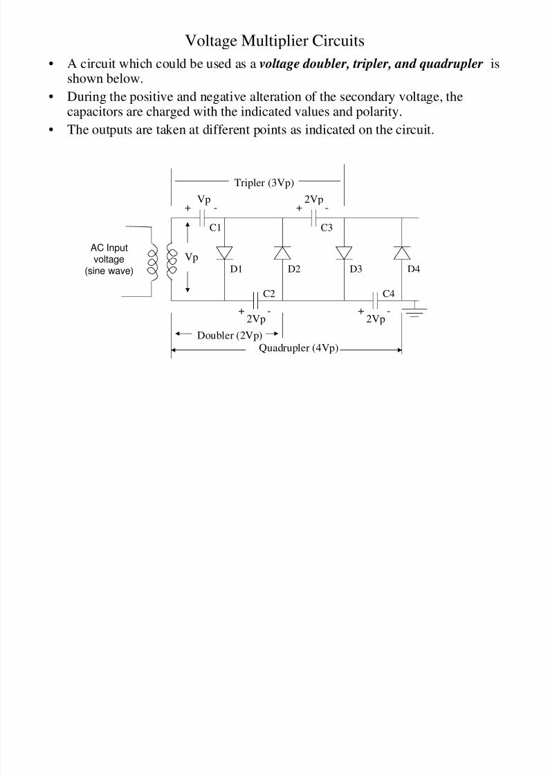
8/7/2019 Electronics 1 Presentation Part 3 (ME)
http://slidepdf.com/reader/full/electronics-1-presentation-part-3-me 98/102
g p g y g ,capacitors are charged with the indicated values and polarity.
• The outputs are taken at different points as indicated on the circuit.
AC Inputvoltage
(sine wave)
Vp
D1
+ -
C1
C2
D3D2 D4
C3
C4
2Vp+ -
2Vp+ - 2Vp+ -
Quadrupler (4Vp)Doubler (2Vp)
Tripler (3Vp)
Vp
Voltage Multiplier Circuits
For the voltage multiplier circuit in the preceding slide:
• During the first positive half of the secondary voltage, D1 is forward biased and current flows from the upper portion of the secondary to C1 to D1 and

8/7/2019 Electronics 1 Presentation Part 3 (ME)
http://slidepdf.com/reader/full/electronics-1-presentation-part-3-me 99/102
g f p f y g , fand current flows from the upper portion of the secondary to C1, to D1, andthen to the lower portion of the secondary. C1 is charged to the peak voltage of
the secondary (Vp) with the indicated polarity. D2 and D4 are reverse biased during this process and does not conduct.
• During the first negative half of the secondary voltage, the voltage across C1(Vp) adds up with the secondary voltage. D2 is forward biased and currentflows from the lower portion of the secondary, to C2, to D2, to C1, and then tothe upper portion of the secondary. C2 is charged to twice the peak voltage of the secondary (2Vp) with the indicated polarity. D1 and D3 are reverse biased
during this process.• During the second positive half of the secondary voltage, the voltage across C2
(2Vp) and the secondary voltage add up while the voltage from C1 (Vp)subtracts from the sum of the two voltages. D3 is forward biased and currentflows from the upper portion of the secondary to C1, to C3, to D3, to C2 , andthen to the lower portion of the secondary. C3 is charged to twice the peakvoltage of the secondary (Vp) with the indicated polarity. D2 and D4 are
reverse biased during this process and does not conduct.
Voltage Multiplier Circuits
For the voltage multiplier circuit in the preceding slide (continuation):
• During the second negative half of the input signal, the secondary voltageadds up with the voltage across C1 and C3 while the voltage across C2

8/7/2019 Electronics 1 Presentation Part 3 (ME)
http://slidepdf.com/reader/full/electronics-1-presentation-part-3-me 100/102
g g f p g y gadds up with the voltage across C1 and C3, while the voltage across C2subtracts from the sum of the voltages. D4 is forward biased and currentflows from the lower portion of the secondary, to C2, to C4, to D4, to C3, toC1, and then to the upper portion of the secondary. C4 is charged to twice
the peak voltage of the secondary (2Vp) with the indicated polarity. D1 andD3 are reverse biased during this process.
• During the succeeding alterations of the secondary voltage, the capacitorsare charged with the indicated voltage and polarity.
• The PIV of the diodes is 2Vp.
• Adding more diodes and capacitors will introduce more voltage multipliersin the circuit.

8/7/2019 Electronics 1 Presentation Part 3 (ME)
http://slidepdf.com/reader/full/electronics-1-presentation-part-3-me 101/102
Zener Diode Applications
Prepared by: Armando V. Barretto
Zener Diode Used For Voltage Regulation
• A circuit using a zener diode for voltage regulation is shown below.

8/7/2019 Electronics 1 Presentation Part 3 (ME)
http://slidepdf.com/reader/full/electronics-1-presentation-part-3-me 102/102
VZ = 5 volts
15 volts
Output Voltage
D1D2
D3 D4
+
-
C1
R1