Embed Size (px)
Citation preview
Electronic Supplementary Information
Flat band potential determination: avoiding the pitfalls
Anna Hankin,*a,c Franky E. Bedoya-Lora,a John C. Alexander,b± Anna Regoutz b and Geoff H. Kelsall a
Departments of Chemical Engineering a and Materialsb, Imperial College London, London, SW7 2AZ. c Institute of Molecular Science and Engineering, Imperial College London
Contents
1. Solution to the Poisson equation for an n-type semiconductor and its application to the semiconductor | electrolyte interface ........ 2
2. Derivation of the Gärtner-Butler equation.............................................................................................................................................. 3
3. Choice of equivalent electrical circuits for CSC determination................................................................................................................. 4
4. Conversion of constant phase elements to capacitance ......................................................................................................................... 7
5. Mott-Schottky analysis of interfacial capacitance, evaluated by electrochemical impedance spectroscopy ......................................... 8
6. Mott-Schottky plots .............................................................................................................................................................................. 10
7. Gärtner-Butler analysis of photocurrents ............................................................................................................................................. 12
8. Analysis of chopped photocurrent measurements ............................................................................................................................... 14
9. Open circuit potential (OCP) measurements ........................................................................................................................................ 17
10. Caution against the use of software-automated impedance analysis at single frequencies ................................................................ 18
11. α-Fe2O3 characterisation by X-ray photoelectron spectroscopy (XPS) .................................................................................................. 19
12. References ............................................................................................................................................................................................ 20
Electronic Supplementary Material (ESI) for Journal of Materials Chemistry A.This journal is © The Royal Society of Chemistry 2019

2
1. Solution to the Poisson equation for an n-type semiconductor and its application to the semiconductor | electrolyte interface
In the absence of interference of surface states, the Mott-Schottky plot will contain contributions from both the semiconductor capacitance and the Helmholtz layer capacitance. The semiconductor capacitance will vary with the degree of band bending while the capacitance of the Helmholtz layer is expected to remain constant. The semiconductor capacitance may be estimated by solving Poisson’s equation1:
𝑑2(∆𝜙SC(𝑥))
𝑑𝑥2= −
𝜌(𝑥)
𝜀0𝜀𝑟
(1)
where ΔϕSC is negative for U > UFB and positive for U < UFB, x is the distance across the depletion region (from surface to the bulk) and ρ is
the charge density, which is computed from the Boltzmann distribution:
𝜌(𝑥) = 𝑒(𝑁𝐷 − 𝑁𝐴 − 𝑛(𝑥) + 𝑝(𝑥)) (2)
where ND and NA are the concentrations of donors and acceptors, respectively, and p(x) and n(x) are the concentrations of electrons and
holes in the conduction and valence bands, respectively:
𝑛(𝑥) = 𝑛0exp 𝑒∆𝜙SC(𝑥)
𝑘B𝑇
(3)
𝑝(𝑥) = 𝑝0exp −𝑒∆𝜙SC(𝑥)
𝑘B𝑇
(4)
where n0 and p0 are the bulk concentrations of electrons and holes in the conduction and valence bands, respectively. Hence, under
depletion, ΔϕSC < 0, electrons are driven into the bulk of the semiconductor (n(x) < n0) while under accumulation, ΔϕSC > 0, electrons
migrate to the surface of the semiconductor (n(x) > n0). The converse is true for holes.
For a semiconductor doped only with donors, ND, integration of equation (1) over the space charge layer1 yields:
𝑑(∆𝜙SC)
𝑑𝑥= [
2𝑒
𝜀0𝜀𝑟
]
12
[−𝑁D ∙ ∆𝜙SC +𝑝0𝑘B𝑇
𝑒(exp −
𝑒∆𝜙SC
𝑘B𝑇 − 1) +
𝑛0𝑘B𝑇
𝑒(exp
𝑒∆𝜙SC
𝑘B𝑇 − 1)]
12
(5)
The differential capacitance of the semiconductor, CSC, is computed according to:
𝐶SC =𝑑𝑄SC
𝑑(∆𝜙SC)
(6)
where QSC may be computed using Gauss’s law:
𝑄SC = 𝜀0𝜀𝑟
𝑑∆𝜙SC
𝑑𝑥
(7)
and hence
𝐶SC = √𝑒𝜀0𝜀𝑟
2
−𝑁D − 𝑝0exp −𝑒∆𝜙SC
𝑘B𝑇 + 𝑛0exp
𝑒∆𝜙SC
𝑘B𝑇
[−𝑁D ∙ ∆𝜙SC +𝑝0𝑘B𝑇
𝑒(exp −
𝑒∆𝜙SC
𝑘B𝑇 − 1) +
𝑛0𝑘B𝑇𝑒
(exp 𝑒∆𝜙SC
𝑘B𝑇 − 1)]
12
(8)
The potential drop across the Helmholtz layer as a function of band bending in the semiconductor is computed according to:
∆𝜙H =𝑄SC
𝐶H
(9)
For understanding experimental measurements, CSC needs to be estimated as a function of Uelectrode rather than ∆𝜙SC. This can be
accomplished using equation (10), in which the potential drops are estimated through the modelling steps above.
𝑈electrode /𝑉(SHE) = 𝑈𝐹𝐵(SHE) + ∆𝜙SC + ∆𝜙H (10)

3
2. Derivation of the Gärtner-Butler equation
A model for the photocurrent flowing across a semiconductor | metal interface2 is also applicable to the semiconductor | liquid junction. The full expression for the total photocurrent, jphoto, generated by monochromatic radiation of intensity I0, accounting for drift current in the depletion layer of width dSC and diffusion current in the bulk of the semiconductor generated over diffusion length Lp is:
𝑗photo = 𝑒𝐼0 [1 − exp(−𝛼 ∙ 𝑑SC)
(1 + 𝛼𝐿p)] +
𝑒𝑝0𝐷p
𝐿p
(11)
dSC is a function of band bending in the semiconductor, ∆𝜙SC, and the depletion layer width constant, 𝑑𝑆𝐶0 (width when 𝜙SC = 1 V):
𝑑SC = 𝑑SC0 ∙ ∆𝜙SC
12
(12)
𝑑SC0 = [
2𝜀0𝜀r
𝑒𝑁D]
12
(13)
Other terms in equation (11) represent the charge of the electron e, diffusion coefficient for holes Dp and the equilibrium concentration of holes in the dark p0. For a wide gap semiconductor, the last term on the right-hand side of equation (11) is often assumed to make a negligible contribution3 as po is negligible relative to no. Therefore, the equation for jphoto simplifies to:
𝑗photo = 𝑒𝐼0 [1 − exp(−𝛼 ∙ 𝑑SC)
(1 + 𝛼𝐿p)]
(14)
A further simplifying assumption is that the diffusion length Lp is much smaller than the absorption depth α and hence αLp ≪ 1, resulting in:
𝑗photo = 𝑒𝐼0[1 − exp(−𝛼 ∙ 𝑑SC)] (15)
The final assumption is that the depletion width is much smaller than the absorption depth and hence 𝛼 ∙ 𝑑SC ≪ 1. This enables the Taylor expansion of exp(−𝛼 ∙ 𝑑SC). Therefore, the underlying assumption of the Gärtner-Butler formulation in equation (16) is that the photocurrent is generated in the depletion region alone.
𝑗photo = 𝑒𝐼0[1 − (1 − 𝛼 ∙ 𝑑SC)] = 𝑒𝛼𝐼0𝑑SC = 𝛼𝐼0 (2𝑒𝜀0𝜀r
𝑁D)
12(∆𝜙SC)
12
(16)
A plot of jph2 against ∆𝜙SC should cross the x-axis at the flat band potential. It should be noted that this relation is only appropriate for the
photocurrent alone rather than the total current. The photocurrent can be obtained by subtracting the dark current from the total current measured under illumination. Alternatively, the photocurrent may be separated from the dark current directly by using a lock-in amplifier synchronized to a chopped light source to remove the dark current. However, due to the transient current that occurs when the illumination changes from light to dark and vice versa, there is considerable error in the magnitude of the measured current.
The eError associated with the unverified assumption that 𝑈 − 𝑈FB ≈ ∆𝜙SC, when interpreting experimental data using equation (16), was discussed in the main manuscript. The determination of ∆𝜙SC as a function of 𝑈 − 𝑈FB can be accomplished using the model described in Section 1 above. Further necessary corrections required by equation (16) have also been described previously4 and include: (i) use of
the spectrally resolved ∑ (𝛼𝜆𝐼0,𝜆)𝜆 product to enable prediction of photocurrent under white light, rather monochromatic light,
illumination; (ii) account for potential-dependent effects of electron–hole recombination rates, decreasing quantum yields, Φ, and (iii) account for the limitation of the predicted current by the absorbed photon flux that would generate a maximum current density of 𝐼0𝑒. These three corrections result in equation (17).
𝑗photo =
𝛷 (2𝑒(∑ (𝛼𝜆𝐼0,𝜆)𝜆 )
2𝜀0𝜀r
𝑁D)
12
(∆𝜙SC)12
[
1 +
𝛷 (2𝑒(∑ (𝛼𝜆𝐼0,𝜆)𝜆 )
2𝜀0𝜀r
𝑁D)
12
(∆𝜙SC)12
𝐼0𝑒
]
(17)

4
3. Choice of equivalent electrical circuits for CSC determination
Circuit 1 (Randles circuit): When a single semicircle is observed on a Nyquist plot generated from EIS data, it is usually modelled using the
equivalent circuit shown in Figure S1. C1 is the interfacial capacitance and can be used with or without correction by the Helmholtz
capacitance5. The real, Z’, and imaginary, -Z’’, components of impedance generated by this circuit are shown in equations (18) and (19),
respectively.
Figure S1. Circuit 1. Randles circuit with one RC loop.
Circuit 1
𝑍′ = 𝑅Faradaic +𝑅1
(1 + 𝜔2𝑅12𝐶1
2) (18)
−𝑍′′ =𝜔𝑅1
2𝐶1
(1 + 𝜔2𝑅12𝐶1
2) (19)
Circuit 2: When two semicircles are observed on a Nyquist plot generated from EIS data, there are multiple equivalent circuit choices.
Figure S2 shows a circuit comprising Faradaic resistance and two RC loops, all in series. In previous work, C1 was assumed to be the
semiconductor capacitance and C2 the Helmholtz capacitance6. The real and imaginary components of impedance generated by this circuit
are shown in equations (20) and (21), respectively.
Figure S2. Circuit 2. Two RC loops in series
Circuit 2
𝑍′ = 𝑅Faradaic +𝑅1
(1 + 𝜔2𝑅12𝐶1
2)+
𝑅2
(1 + 𝜔2𝑅22𝐶2
2) (20)
−𝑍′′ =𝜔𝑅1
2𝐶1
(1 + 𝜔2𝑅12𝐶1
2)+
𝜔𝑅22𝐶2
(1 + 𝜔2𝑅22𝐶2
2) (21)
RFaradaic
C1
R1
C2
R2

5
Circuit 3: Figure S3 shows a different circuit that would generate two Nyquist semicircles (two time constants), which contains an RC loop
in parallel with C1; this circuit has been used to explain charge trapping by surface states7 as the second RC loop dominates the impedance
at low frequencies. The real and imaginary components of impedance generated by this circuit are shown in equations (22) and (23),
respectively.
Figure S3. Circuit 3. R2C2 loop in parallel with C1.
Circuit 3
𝒁′ = 𝑅Faradaic +[(𝑅1 + 𝑅2)(1 − 𝜔2𝑅1𝑅2𝐶1𝐶2)𝜔2(𝑅1𝐶1 + 𝑅2𝐶1 + 𝑅2𝐶2)
2 +𝑅1𝑅2𝐶2
(𝑅1𝐶1 + 𝑅2𝐶1 + 𝑅2𝐶2)]
[1 +(1 − 𝜔2𝑅1𝑅2𝐶1𝐶2)
2
𝜔2(𝑅1𝐶1 + 𝑅2𝐶1 + 𝑅2𝐶2)2]
(22)
−𝒁′′ =[𝑅1𝑅2𝐶2(1 − 𝜔2𝑅1𝑅2𝐶1𝐶2)𝜔(𝑅1𝐶1 + 𝑅2𝐶1 + 𝑅2𝐶2)
2 −𝑅1 + 𝑅2
𝜔(𝑅1𝐶1 + 𝑅2𝐶1 + 𝑅2𝐶2)]
[1 +(1 − 𝜔2𝑅1𝑅2𝐶1𝐶2)
2
𝜔2(𝑅1𝐶1 + 𝑅2𝐶1 + 𝑅2𝐶2)2]
(23)
Circuit 4: Figure S4 shows a circuit that for many decades has been proposed for describing charge trapping by surface states8-10. In this
case, the additional resistor and capacitor are in series with each other but collectively in parallel with C1. The real and imaginary
components of impedance generated by this circuit are shown in equations (24) and (25), respectively.
Figure S4. Circuit 4. A second resistor and capacitor in parallel with C1.
Circuit 4
𝑍′ = 𝑅Faradaic +𝜔2𝑅1𝑅2𝐶2(𝑅1𝐶1 + 𝑅1𝐶2 + 𝑅2𝐶2) − 𝑅1(𝜔
2𝑅1𝑅2𝐶1𝐶2 − 1)
[𝜔2(𝑅1𝐶1 + 𝑅1𝐶2 + 𝑅2𝐶2)2 + (𝜔2𝑅1𝑅2𝐶1𝐶2 − 1)2]
(24)
−𝑍′′ =[𝜔𝑅1𝑅2𝐶2(𝜔
2𝑅1𝑅2𝐶1𝐶2 − 1) + 𝜔𝑅1(𝑅1𝐶1 + 𝑅1𝐶2 + 𝑅2𝐶2)]
[𝜔2(𝑅1𝐶1 + 𝑅1𝐶2 + 𝑅2𝐶2)2 + (𝜔2𝑅1𝑅2𝐶1𝐶2 − 1)2]
(25)
RFaradaic
C1
R1
C2
R2
RFaradaicC1
R1
R2 C2

6
Circuit simulations: The Nyquist plots generated for equivalent circuits 1, 2, 3 and 4 for identical values of RFaradaic, R1, C1 and R2 but varying
values of C2, are compared in Figure S5. Only circuits 2 and 3 can describe the impedance obtained across the α-Fe2O3 | 1 M NaOH interface
(Figure 8 in the main manuscript), which at all applied potentials exhibited low impedance semicircles at high frequencies and high
impedance semicircles at low frequencies.
Circuits 2 and 3 yield identical Nyquist plots when C1 << C2. However, when C2 becomes comparable in value to C1, the extents of overlap
between the high and low frequency semicircles differ markedly for the two circuits. Hence, when data can be modelled only using one
of these circuits and not the other, the presence of an additional capacitance of similar value to CSC is essentially confirmed.
(a) RFaradaic = 40 Ω m2, R1 = 300 Ω m2, C1 = 10-6 F m-2, R2=104 Ω m2, C2 = 10-3 F m-2
(b) RFaradaic = 40 Ω m2, R1 = 300 Ω m2, C1 = 10-6 F m-2, R2=104 Ω m2, C2 = 10-4 F m-2
(c) RFaradaic = 40 Ω m2, R1 = 300 Ω m2, C1 = 10-6 F m-2, R2=104 Ω m2, C2 = 10-5 F m-2
(d) RFaradaic = 40 Ω m2, R1 = 300 Ω m2, C1 = 10-6 F m-2, R2=104 Ω m2, C2 = 10-6 F m-2
Figure S5. Nyquist plots generated for circuits 1, 2, 3 and 4 using RFaradaic = 40 Ω m2, R1 = 300 Ω m2, C1 = 10-6 F m-2, R2=104 Ω m2 and varying values of C2. For simplicity, the electrode area was set to 1 m2.
0
200
400
600
800
1,000
0 200 400 600 800 1,000
-Z'' / Ω
m2
Z' / Ω m2
[R(C[R(RC)])] Circuit model
[R(RC)(RC)] Circuit model
[R(RC)] Circuit model
[R(R(C)[C[R]])] circuit model
0
100
200
300
400
0 100 200 300 400
0
200
400
600
800
1,000
0 200 400 600 800 1,000
-Z'' / Ω
m2
Z' / Ω m2
[R(C[R(RC)])] Circuit model
[R(RC)(RC)] Circuit model
[R(RC)] Circuit model
[R(R(C)[C[R]])] circuit model
0
100
200
300
400
0 100 200 300 400
0
200
400
600
800
1,000
0 200 400 600 800 1,000
-Z''
/ Ω
m2
Z' / Ω m2
[R(C[R(RC)])] Circuit model
[R(RC)(RC)] Circuit model
[R(RC)] Circuit model
[R(R(C)[C[R]])] circuit model
0
100
200
300
400
0 100 200 300 400
0
200
400
600
800
1,000
0 200 400 600 800 1,000
-Z''
/ Ω
m2
Z' / Ω m2
[R(C[R(RC)])] Circuit model
[R(RC)(RC)] Circuit model
[R(RC)] Circuit model
[R(R(C)[C[R]])] circuit model
0
100
200
300
400
0 100 200 300 400
7
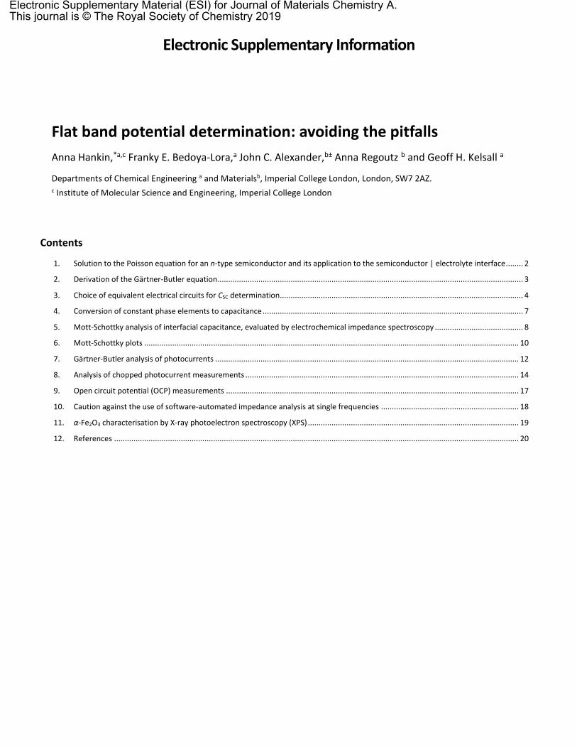
4. Conversion of constant phase elements to capacitance
Constant phase elements, CPEs, are used in place of capacitors for fitting equivalent circuits to experimentally determined impedance
data, when non-ideal capacitive behaviour is observed, manifested in ‘depressed’ semicircles in Nyquist plots. The impedance of a
constant phase element is given in equation (26). Q0 has the units of admittance; the exponent n defines the extent of capacitive
behaviour: n = 1 for a perfect capacitor and n = 0 for a perfect resistor.
There are two possible approaches for converting CPE to capacitance; both have been applied to interfacial modelling of electrochemical
systems:
(i) In the case in which the CPE is modelled to be in parallel with a resistor, the resistance corresponds to the width of the semicircle
(along the Z’ axis) and its value is used in the conversion11-13, as shown in equation (27);
(ii) Instead of resistance, the angular frequency at which the maximum in the imaginary component of the semicircle occurs, ωmax, can be
used as shown in equation (28), where ωmax may be determined from plots of complex impedances against the logarithm of the
frequency at which they are measured14.
𝑍(CPE) =1
𝑄0(𝑗𝜔)𝑛 (26)
𝐶 = 𝑄0
1𝑛𝑅
(1−𝑛)𝑛 (27)
𝐶 = 𝑄0(𝜔max′′ )𝑛−1 (28)
We modelled all our EIS data using the [RFaradaic(C1[R1(R2C2)])] circuit (circuit 3), in which both capacitors needed to be replaced with CPEs to enable a good fit. Equation (28) was not used because ωmax could not be reliably determined from plots of Z’’ against log(f), as shown in Figure S6(a) for Sample 2. We used equation (27); the quality of the circuit fit to experimental data is shown in Figure S6(b) and extent of capacitances, n, for two loops in Figure S6 (c) and (d). For most applied potentials, n1, was > 0.8.
(a) (b)
(c) (d)
Figure S6. Plot of Z’’ against log(f) using raw EIS data collected across the α-Fe2O3 (Sample 2) | 1 M NaOH interface; the quality of the [RFaradaic(CPE1[R1(R2CEP2)])] circuit fit to experimental data, χ2 (b) and numerical information extracted from the fitting: n1 (c) and n2 (d).
1
10
100
1000
10000
100000
1000000
-2 -1 0 1 2 3 4 5 6
-Z‘’
/ Ω
Frequency, f / Hz
0
0.01
0.02
0.03
0.04
0.05
0.06
0.07
0.08
0.09
0.1
-0.4 -0.3 -0.2 -0.1 0 0.1 0.2 0.3 0.4 0.5 0.6 0.7 0.8 0.9 1
χ2
Electrode potential, U (SHE) / V
Sample 1
Sample 2
Sample 3
0
0.1
0.2
0.3
0.4
0.5
0.6
0.7
0.8
0.9
1
-0.4 -0.3 -0.2 -0.1 0 0.1 0.2 0.3 0.4 0.5 0.6 0.7 0.8 0.9 1
n1
Electrode potential, U (SHE) / V
Sample 1
Sample 2
Sample 3
0
0.1
0.2
0.3
0.4
0.5
0.6
0.7
0.8
0.9
1
-0.4 -0.3 -0.2 -0.1 0 0.1 0.2 0.3 0.4 0.5 0.6 0.7 0.8 0.9 1
n2
Electrode potential, U (SHE) / V
Sample 1
Sample 2
Sample 3

8
Since n1 < 1, the use of equation (27) is not strictly accurate, as it does not take into account the additional impedance of the R2C2 loop, which is in series with R1 (see Figure S3). However, equation (27) should yield a sufficiently accurate result, provided Z’(R2C2) << R1 at ωmax. This can be proven if ωmax is known; however, as shown in Figure S6(a), this is not always straightforward. Hence, to verify the accuracy of our CPE to C conversion, we determined ωmax using the distribution of relaxation times, DRT, for EIS data collected at three applied electrode potentials on Sample 2. The DRT method15-17 is relatively novel and requires complex processing of impedance data. We employed open-access MATLAB-based DRT software ‘DRTTOOLS’15, 18 to determine ωmax, and subsequently to compute C1 using equation (28). Results are presented in Table S1 and confirm that Z’(R2C2) << R1 at ωmax. The Mott-Schottky plots generated using the two approaches are compared in Figure S7 and show that the capacitance values extracted from CPEs were reliable and cannot be expected to make a significant contribution to the error in flat band determination.
Table S1: Analysis of EIS data collected on α-Fe2O3 Sample 2 in 1 M NaOH using circuit fitting and distribution of relaxation times. (*) Capacitance determined using equation (27); (**) Capacitance determined using equation (28).
Applied potential
(SHE) / V
[RFaradaic(CPE1[R1(R2CPE2)])] circuit fitting DRT fitting Combined data from both fittings
R1 / Ω 𝑪𝐈𝐧𝐭𝐞𝐫𝐟𝐚𝐜𝐞−𝟐 (*) / Ω m2 ωmax / rad s-1 Z’(R2C2) at ωmax / Ω 𝑪𝐈𝐧𝐭𝐞𝐫𝐟𝐚𝐜𝐞
−𝟐 (**) / Ω m2
-0.253 180 507 8 577 1.00 × 10⁻² 544
-0.053 689 634 2 769 3.07 × 10⁻² 686
+0.197 2 220 947 1 100 7.08 × 10⁻¹³ 993
Figure S7. Mott-Schottky plots based on EIS data collected on α-Fe2O3 Sample 2 in 1 M NaOH and processed
using circuit fitting () and distribution of relaxation times, DRT ().
5. Mott-Schottky analysis of interfacial capacitance, evaluated by electrochemical impedance spectroscopy
EIS measurements were performed on three hematite samples in 1 M NaOH in the dark at potentials in the range -0.3 to +0.8 V (SHE).
Each applied potential was perturbed sinusoidally by ±10 mV (p-p) at 75 frequencies in the range 10-1 - 105 Hz. Prior to the fitting of the
[RFaradaic(CPE1[R1(R2CPE2)])] equivalent circuit to EIS data, the number of data points used for analysis per data set was decreased. Firstly,
data collected at applied frequencies higher than 18.6 kHz (10 data points) was removed; these data varied negligibly with applied
400
500
600
700
800
900
1,000
1,100
1,200
1,300
1,400
-0.4 -0.3 -0.2 -0.1 0 0.1 0.2 0.3 0.4 0.5 0.6
1 /
C2
[ m
4F-2
]
Electrode potential, U (SHE) / V
Circuit fitting
DRT (-0.253 V(SHE))
DRT (-0.053 V(SHE))
DRT (+0.197 V(SHE))

9
potential, as demonstrated in Figure S8, and were believed to be a contribution from the reference electrode. Additionally, data points
collected at frequencies below 1.65 Hz (15 data points) were also removed; the additional time constant observed for some potentials at
these low frequencies could not be explained and required an unjustifiably complex equivalent circuit. In the end, the
[RFaradaic(CPE1[R1(R2CPE2)])] equivalent circuit was fitted to 50 data points per data set, spanning five decades of applied frequencies, which
was considered sufficient for accurate determination of 5 circuit elements.
(a) (b)
Figure S8. Features observed in impedance data obtained at perturbation frequencies higher than ≈ 18.6 kHz across the potential range -0.3 V ≤ V (SHE) ≤ +0.9. These features were excluded from analysis by equivalent circuit fitting. The independence of these features from applied potential is demonstrated in (a) Nyquist plot and (b) Bode phase plot.
Details of the equivalent circuit fitting are shown in Figure S9 for the example of data collected on α-Fe2O3 Sample 2 at 0 V (SHE); these
data were qualitatively representative of measurements at other potentials.
(a) (b)
(c) (d)
Figure S9. Bode phase plot (a) and Nyquist plots (b – d) of raw ( ) and modelled ( ) EIS data collected on α-Fe2O3 Sample 2 at 0 V (SHE). The modelled data show the range of data used for circuit fitting.
0.00040 0.00045 0.00050
0.0000
0.0001
0.0002
0.0003
0.0004
0.0005
-Z"
/
m2
Z' / m2
-0.253
-0.203
-0.153
-0.103
-0.053
-0.003
0.047
0.097
0.147
0.197
0.247
0.297
0.347
0.397
0.447
0.497
0.547
0.597
0.647
0.697
0.747
0.797
Data excluded from fitting
18.6 kHz
0 20000 40000 60000 80000 100000
0
10
20
30
40
50
60
70
-Ph
ase
/ o
Frequency / Hz
18.6 kHz
Data excluded from fitting
0
10
20
30
40
50
60
70
80
90
0.01 0.1 1 10 100 1000 10000 100000
-Ph
ase
/ o
Frequency / Hz
Modelled data
18.6 kHz1.65 Hz
RFaradaic
CPE1
CPE2
R2
R1
Raw data
Fitted curve
0
0.5
1
1.5
2
2.5
3
3.5
0 0.1 0.2 0.3 0.4 0.5 0.6
-Z"
/ Ω
m2
Z' / Ω m2
Applied potential ≈ 0 V (SHE)
1.65 Hz
0.1 Hz
0.3 Hz
0
0.1
0.2
0.3
0.4
0.5
0.6
0 0.1 0.2 0.3 0.4 0.5 0.6
-Z"
/ Ω
m2
Z' / Ω m2
1.65 Hz
0
0.005
0.01
0.015
0.02
0 0.005 0.01 0.015 0.02
-Z"
/ Ω
m2
Z' / Ω m2
18.6 kHz
47 Hz
145 Hz
780 Hz
0
0.0005
0.001
0.0015
0.002
0 0.0005 0.001 0.0015 0.002
18.6 kHz2.39 kHz

10
6. Mott-Schottky plots
Mott-Schottky plots of 𝐶−2 vs. E are shown for three α-Fe2O3 samples in 1 M NaOH in Figure S10 and for an FTO sample in 1 M NaOH in
Figure S11. Comparison between these figures shows that FTO is unlikely to have influenced the impedance spectra recorded on hematite
and hence was not responsible for the spread in determined flat band potentials.
(a) (b)
(c) (d)
Figure S10. Mott-Schottky plots from interfacial capacitance of α-Fe2O3 in 1 M NaOH: (a) uncorrected for CH and corrected for CH = (b) 0.20 F m-2, (c) 0.15 F m-2, (d) 0.10 F m-2.
Figure S11. Mott-Schottky plot from interfacial capacitance of FTO in 1 M NaOH.
0
200
400
600
800
1,000
1,200
1,400
1,600
-0.8 -0.6 -0.4 -0.2 0 0.2 0.4 0.6 0.8 1
1 /
C2
[ m
4F-2
]
Electrode potential, U (SHE) / V
Sample 1
Sample 2
Sample 3
0
200
400
600
800
1,000
1,200
1,400
1,600
-0.8 -0.6 -0.4 -0.2 0 0.2 0.4 0.6 0.8 1
1 /
C2
[ m
4F-2
]
Electrode potential, U (SHE) / V
Sample 1
Sample 2
Sample 3
0
200
400
600
800
1,000
1,200
1,400
1,600
-0.8 -0.6 -0.4 -0.2 0 0.2 0.4 0.6 0.8 1
1 /
C2
[ m
4F-2
]
Electrode potential, U (SHE) / V
Sample 1
Sample 2
Sample 3
0
200
400
600
800
1,000
1,200
1,400
1,600
-0.8 -0.6 -0.4 -0.2 0 0.2 0.4 0.6 0.8 1
1 /
C2
[ m
4F-2
]
Electrode potential, U (SHE) / V
Sample 1
Sample 2
Sample 3
0
2
4
6
8
10
12
14
16
-1.4 -1.2 -1 -0.8 -0.6 -0.4 -0.2 0 0.2 0.4 0.6 0.8 1
1 /
C2
[ m
4F-2
]
Electrode potential, U (SHE) / V

11
Table S2 lists flat band potentials and charge carrier densities derived from data presented in Figure S10 and Figure S11. Accounting for
the range of feasible Helmholtz layer capacitances and assuming that εr = 80 for the semiconductor, the range in flat band potentials and
charge carrier densities of hematite was -0.77 to -0.32 V (SHE) and 1.47 × 1025 to 2.61 × 1025 m-3, respectively. Based on these data and
their wide dispersion, it is unreasonable to suggest a specific flat band potential value.
Table S2: Flat band potentials and charge carrier densities determined for α-Fe2O3 and FTO in 1 M NaOH using Mott-Schottky analysis (εr = 80 assumed).
Uncorrected CH = 0.20 F m-2 CH = 0.15 F m-2 CH = 0.10 F m-2
Fe2O3 (Sample 1) Flat band potential (SHE) / V -0.59 -0.44 -0.40 -0.32
Donor density / m-3 1.64 × 1025 2.01 × 1025 2.18 × 1025 2.61 × 1025
Fe2O3 (Sample 2) Flat band potential (SHE) / V -0.69 -0.56 -0.52 -0.43
Donor density / m-3 1.63 × 1025 1.96 × 1025 2.10 × 1025 2.46 × 1025
Fe2O3 (Sample 3) Flat band potential (SHE) / V -0.77 -0.65 -0.61 -0.52
Donor density / m-3 1.47 × 1025 1.80 × 1025 1.91 × 1025 2.20 × 1025
FTO Flat band potential (SHE/ V) -1.29 - - -
Application of the interfacial model to experimentally determined interfacial capacitance data
The interfacial model presented in Section 1 can be used to decrease the spread in the values presented in Table S2. Figure S12 and Table
S3 show that the interfacial model was used successfully to narrow the ranges of flat band potentials and dopant densities of our hematite
samples in 1 M NaOH to -0.77 to -0.50 V (SHE) and 1.50 × 1025 to 1.70 × 1025 m-3, respectively. Mott-Schottky plots for each sample and
different assumed values of CH (0.1 – 0.2 F m-2) can be modelled using just one charge carrier density. If a different value of εr is used in
the model, the charge carrier density changes without affecting the flat band potential. The interfacial model enabled the dispersion in
flat band potentials to be decreased from 0.45 V to 0.27 V, a significant improvement. However, further increase in confidence is required
through other flat band potential determination methods.
(a) (b)
Figure S12. Experimentally determined () and simulated Mott-Schottky plots based on semiconductor (---) and interfacial (- ⸱ - ⸱ -) capacitances for (a) hematite Sample 1 and (b) hematite Sample 2.
Table S3: Modelled flat band potentials and charge carrier densities for α-Fe2O3 samples (εr = 80 assumed).
CH = 0.20 F m-2 CH = 0.15 F m-2 CH = 0.10 F m-2
Fe2O3 (Sample 1) Flat band potential (SHE) / V -0.57 -0.56 -0.50
Donor density / m-3 1.70 × 1025 1.70 × 1025 1.70 × 1025
Fe2O3 (Sample 2) Flat band potential (SHE) / V -0.63 -0.61 -0.57
Donor density / m-3 1.55 × 1025 1.55 × 1025 1.55 × 1025
Fe2O3 (Sample 3) Flat band potential (SHE) / V -0.77 -0.74 -0.70
Donor density / m-3 1.50 × 1025 1.50 × 1025 1.50 × 1025
0
200
400
600
800
1,000
1,200
1,400
-0.8 -0.6 -0.4 -0.2 0 0.2 0.4 0.6 0.8
1 /
C2
[ m
4F-2
]
Electrode potential, U (SHE) / V
CH = infinitely high
CH = 0.20 F m-2
CH = 0.15 F m-2
CH = 0.10 F m-2
0
200
400
600
800
1,000
1,200
1,400
1,600
-0.8 -0.6 -0.4 -0.2 0 0.2 0.4 0.6 0.8 1
1 /
C2
[ m
4F-2
]
Electrode potential, U (SHE) / V
CH = infinitely high
CH = 0.20 F m-2
CH = 0.15 F m-2
CH = 0.10 F m-2

12
7. Gärtner-Butler analysis of photocurrents
In 1 M NaOH: Net photocurrents measured on hematite and FTO in 1 M NaOH at different scan rates are shown in Figure S13.
(a-1) (a-2)
(b-1) (b-2)
(c-1) (c-2)
(d-1) (d-2)
Figure S13. Effects of electrode potential and scan rate on net photocurrents and their squares for hematite Samples 1 (a-1 & a-2), Sample 2 (b-1 & b-2) and
Sample 3 (c-1 & c-2) in 1 M NaOH and FTO in 1 M NaOH (d-1 & d-2). Dashed lines indicate the extrapolation of the linear portions of 𝑗photo2 to the x-axis.
0
2
4
6
8
10
12
14
16
18
20
-0.4 -0.2 0 0.2 0.4 0.6 0.8 1
Net
ph
oto
curr
en
t d
en
sity
, j p
ho
to/
A m
-2
Electrode potential, U / V vs SHE
100 mV/s
50 mV/s
10 mV/s
1 mV/s
Direction of scan
100 mV s-1
50 mV s-1
10 mV s-1
1 mV s-1
0
1
2
3
4
5
-0.2 -0.1 0 0.1 0.2
0
50
100
150
200
250
300
350
400
0 0.1 0.2 0.3 0.4 0.5 0.6 0.7 0.8 0.9 1
Ph
oto
curr
en
t sq
uar
ed
, j p
ho
to2
/ A
2m
-4
Electrode potential, U / V vs SHE
100 mV/s
50 mV/s
10 mV/s
1 mV/s
100 mV s-1
50 mV s-1
10 mV s-1
1 mV s-1
0
2
4
6
8
10
12
14
16
18
20
-0.4 -0.2 0 0.2 0.4 0.6 0.8 1
Net
ph
oto
curr
en
t d
en
sity
, j p
ho
to/
A m
-2
Electrode potential, U / V vs SHE
100 mV/s
50 mV/s
10 mV/s
1 mV/s
100 mV s-1
50 mV s-1
10 mV s-1
1 mV s-1
0
1
2
3
4
5
-0.2 -0.1 0 0.1 0.2
0
50
100
150
200
250
300
350
400
0 0.1 0.2 0.3 0.4 0.5 0.6 0.7 0.8 0.9 1
Ph
oto
curr
en
t sq
uar
ed
, jp
ho
to2
/ A
2m
-4
Electrode potential, U / V vs SHE
100 mV/s
50 mV/s
10 mV/s
1 mV/s
100 mV s-1
50 mV s-1
10 mV s-1
1 mV s-1
-0.25
-0.20
-0.15
-0.10
-0.05
0.00
0.05
0.10
0.15
0.20
-0.4 -0.2 0 0.2 0.4 0.6 0.8 1
Net
ph
oto
curr
en
t d
en
sity
, j p
ho
to/
A m
-2
Electrode potential, U / V vs SHE
100 mV/s
50 mV/s
10 mV/s
100 mV s-1
50 mV s-1
10 mV s-1
0.000
0.005
0.010
0.015
0.020
0 0.1 0.2 0.3 0.4 0.5 0.6 0.7 0.8 0.9 1
Ph
oto
curr
en
t sq
uar
ed
, j p
ho
to2
/ A
2m
-4
Electrode potential, U / V vs SHE
100 mV/s
50 mV/s
10 mV/s
100 mV s-1
50 mV s-1
10 mV s-1
0.E+00
1.E-03
2.E-03
3.E-03
4.E-03
5.E-03
0.05 0.15 0.25

13
In 1 M NaOH + 0.5 M H2O2: Figure S14 shows net photocurrents measured on hematite in 1 M NaOH containing 0.5 M H2O2 at different
scan rates. No photocurrent could be determined of FTO in this electrolyte at any scan rate.
(a-1) (a-2)
(b-1) (b-2)
(c-1) (c-2)
Figure S14. Effects of applied potential and scan rate on net photocurrents and their squares for hematite samples 1 (a-1 & a-2), 2 (b-1 & b-2) and 3 (c-1 & c-2)
in 1 M NaOH. Dashed lines indicate the extrapolation of the linear portions of 𝑗photo2 to the potential axis.
Summary of flat band potentials determined by Gärtner-Butler analysis
Table S4: Flat band potentials determined by Gärtner-Butler analysis for α-Fe2O3 and FTO samples in 1 M NaOH in absence and presence of 0.5 M H2O2
Flat band potential (SHE) / V
1 M NaOH 1 M NaOH + 0.5 M H2O2
100 mV s-1 50 mV s-1 10 mV s-1 1 mV s-1 100 mV s-1 50 mV s-1 10 mV s-1 1 mV s-1
Fe2O3 (Sample 1) +0.24 +0.24 +0.25 +0.25 -0.36 -0.37 -0.34 -0.34
Fe2O3 (Sample 2) +0.30 +0.32 +0.33 +0.34 -0.44 -0.42 -0.41 -0.39
Fe2O3 (Sample 3) +0.26 +0.28 +0.28 +0.29 -0.45 -0.43 -0.42 -0.40
FTO +0.13 +0.11 +0.07 - - - - -
0
5
10
15
20
25
-0.4 -0.2 0 0.2 0.4 0.6 0.8 1
Net
ph
oto
curr
ent
den
sity
, j p
ho
to/
A m
-2
Electrode potential, U / V vs SHE
100 mV/s
50 mV/s
10 mV/s
1 mV/s
100 mV s-1
50 mV s-1
10 mV s-1
1 mV s-1
Direction of scan
0
50
100
150
200
250
300
350
400
450
-0.5 -0.4 -0.3 -0.2 -0.1 0 0.1 0.2 0.3 0.4 0.5 0.6 0.7 0.8 0.9 1
Ph
oto
curr
en
t sq
uar
ed
, j p
ho
to2
/ A
2m
-4
Electrode potential, U / V vs SHE
100 mV/s
50 mV/s
10 mV/s
1 mV/s
100 mV s-1
50 mV s-1
10 mV s-1
1 mV s-1
0
5
10
15
20
25
-0.4 -0.2 0 0.2 0.4 0.6 0.8 1
Net
ph
oto
curr
ent
den
sity
, j p
ho
to/
A m
-2
Electrode potential, U / V vs SHE
100 mV/s
50 mV/s
10 mV/s
1 mV/s
100 mV s-1
50 mV s-1
10 mV s-1
1 mV s-1
0
50
100
150
200
250
300
350
400
450
-0.5 -0.4 -0.3 -0.2 -0.1 0 0.1 0.2 0.3 0.4 0.5 0.6 0.7 0.8 0.9 1
Ph
oto
curr
en
t sq
uar
ed
, j p
ho
to2
/ A
2m
-4
Electrode potential, U / V vs SHE
100 mV/s
50 mV/s
10 mV/s
1 mV/s
100 mV s-1
50 mV s-1
10 mV s-1
1 mV s-1
0
5
10
15
20
25
-0.4 -0.2 0 0.2 0.4 0.6 0.8 1
Net
ph
oto
curr
ent
de
nsi
ty,
j ph
oto
/ A
m-2
Electrode potential, U / V vs SHE
100 mV/s
50 mV/s
10 mV/s
1 mV/s
100 mV s-1
50 mV s-1
10 mV s-1
1 mV s-1
0
50
100
150
200
250
300
350
400
450
-0.5 -0.4 -0.3 -0.2 -0.1 0 0.1 0.2 0.3 0.4 0.5 0.6 0.7 0.8 0.9 1
Ph
oto
curr
en
t sq
uar
ed
, j p
ho
to2
/ A
2m
-4
Electrode potential, U / V vs SHE
100 mV/s
50 mV/s
10 mV/s
1 mV/s
100 mV s-1
50 mV s-1
10 mV s-1
1 mV s-1

14
8. Analysis of chopped photocurrent measurements
Chopped photocurrents on hematite in 1 M NaOH solution
In addition to the previously observed steady state photocurrents at U > -0.1 V (SHE) in 1 M NaOH, the hematite samples exhibited
transient photocurrents in the potential region ca. -0.38 ≤ U (SHE) / V≤ -0.15.
(a) (b)
Figure S15. Effect of potential on chopped photocurrents recorded on three hematite samples in 1 M NaOH at a chopping frequency of 0.3 Hz and scan rate of 1 mV s-1. Two regions where photocurrent was observed are shown in (a) and (b).
Chopped photocurrents on hematite in 1 M NaOH + 0.5 H2O2 solution
As shown in Figure S16, the transient photocurrents observed in 1 M NaOH were not observed in the presence of the H2O2 hole scavenger.
(a) (b)
Figure S16. Effect of potential on chopped photocurrents recorded on three hematite samples in 1 M NaOH + 0.5 M H2O2 at a chopping frequency of 0.3 Hz and scan rate of 1 mV s-1.
-0.6
-0.5
-0.4
-0.3
-0.2
-0.1
0.1
0.2
0.3
-0.45 -0.4 -0.35 -0.3 -0.25 -0.2 -0.15 -0.1 -0.05 0
Cu
rren
t d
en
sity
, j
/ A
m-2
Electrode potential, U / V vs SHE
UFB
UFB
UFBDirection of scan
Sample 1
Sample 2
Sample 3
-2
0
2
4
6
8
10
12
14
-0.3 -0.2 -0.1 0 0.1 0.2 0.3 0.4 0.5 0.6 0.7 0.8 0.9
Cu
rren
t d
en
sty,
j/
A m
-2
Electrode potential, U / V vs SHE
Sample 1
Sample 2
Sample 3
-90
-80
-70
-60
-50
-40
-30
-20
-10
0
-0.5 -0.45 -0.4 -0.35 -0.3 -0.25
Cu
rren
t d
en
sity
, j
/ A
m-2
Electrode potential, U / V vs SHE
UFB
UFB
UFB
Sample 1
Sample 2
Sample 3
-120
-100
-80
-60
-40
-20
0
20
40
60
-0.5 -0.3 -0.1 0.1 0.3 0.5 0.7 0.9
Cu
rren
t d
ensi
ty,
j/
A m
-2
Electrode potential, U / V vs SHE
Sample 1
Sample 2
Sample 3

15
Chopped photocurrent on FTO in 1 M NaOH solution
(a) (b)
Figure S17. Effect of potential on chopped photocurrent recorded on FTO in 1 M NaOH at a chopping frequency of 0.3 Hz and scan rate of 1 mV s-1. The shaded region in plot (a) shows the uncertainty in the potential at which photocurrent switched from being negative relative to dark current to being positive relative to dark current.
Chopped photocurrent on FTO in 1 M NaOH + 0.5 M H2O2 solution
In these conditions, the photocurrent on FTO was barely distinguishable from dark current and the flat band potential could not be
determined.
Figure S18. Chopped photocurrent recorded on FTO in 1 M NaOH + 0.5 H2O2 at a chopping frequency of 0.3 Hz and scan rate of 1 mV s-1.
Summary of flat band potentials determined through chopped photocurrent measurements
The flat band potential values determined on hematite and FTO in the absence and presence of H2O2 are reported in Table S5.
Table S5: Flat band potentials determined from chopped photocurrent voltammetry for α-Fe2O3 and FTO samples in 1 M NaOH in absence and presence of 0.5 M H2O2
Flat band potential (SHE) / V
1 M NaOH 1 M NaOH + 0.5 M H2O2
Fe2O3 (Sample 1) -0.38 -0.40
Fe2O3 (Sample 2) -0.40 -0.39
Fe2O3 (Sample 3) -0.39 -0.47
FTO -0.33 -
-0.45
-0.40
-0.35
-0.30
-0.25
-0.20
-0.4 -0.38 -0.36 -0.34 -0.32 -0.3 -0.28
Cu
rre
nt
de
nsi
ty,
j/
A m
-2
Electrode potential, U / V vs SHE
UFB
-1.2
-1.0
-0.8
-0.6
-0.4
-0.2
0.0
0.2
-0.6 -0.5 -0.4 -0.3 -0.2 -0.1 0 0.1 0.2 0.3 0.4 0.5 0.6 0.7 0.8 0.9
Cu
rre
nt
de
nsi
ty,
j/
A m
-2
Electrode potential, U / V vs SHE
-0.10
-0.05
0.00
0.05
0.10
0.15
-0.2 -0.1 0 0.1 0.2 0.3 0.4 0.5 0.6 0.7 0.8 0.9
-40
-30
-20
-10
0
10
20
30
-0.6 -0.5 -0.4 -0.3 -0.2 -0.1 0 0.1 0.2 0.3 0.4 0.5 0.6 0.7 0.8 0.9
Cu
rre
nt
de
nsi
ty,
j/
A m
-2
Electrode potential, U / V vs SHE
0.30
0.32
0.34
0.36
0.38
0.40
0.35 0.36 0.37 0.38 0.39 0.4

16
Chopped photocurrents on hematite in 1 M NaOH solution under monochromatic illumination
Chopped photocurrent recorded under monochromatic conditions (λ = 360, 450, 570 and 620 nm) suggested an absence of any bulk inter-
band gap states that may have affected the photoelectrode performance, as well as the characteristics of its interface with the electrolyte.
Light with energy less than the energy of the band gap (EG ≈ 2.1 eV => λ ≈ 590 nm) generated negligible photocurrent.
Figure S19. Chopped photocurrent recorded on hematite in 1 M NaOH, under monochromatic light of different wavelengths; scan rate of 1 mV s-1 and chopping frequency of 0.3 Hz were used.

17
9. Open circuit potential (OCP) measurements
OCP measurements on hematite and FTO in 1 M NaOH and 1 M NaOH + 0.5 M H2O2 solutions
Figure S20 shows the effects of irradiance and electrolyte composition on the OCP recorded on hematite and FTO. Table S6 shows the
extracted flat band potentials. Deoxygenation of the electrolyte was found to affect the measured OCP in the dark and under low
irradiance, confirming that such measurements require high illumination intensity; the concentration of dissolved oxygen in the
electrolyte affects its electrode potential, which in turn affects the Fermi level of the semiconductor upon equilibration, until the
illumination is sufficiently strong to control band bending.
(a) (b)
(c) (d)
Figure S20. Effects of irradiance (0 – 2815 W m-2) and electrolyte composition on open circuit potentials of hematite: (a) Sample 1, (b) Sample 2, (c) Samples 3, and FTO: (d). The effect of electrolyte de-oxygenation is shown in (c) for Sample 3.
Summary of flat band potentials determined through OCP measurements
Table S6: Flat band potentials determined from open circuit potentials of α-Fe2O3 and FTO samples in 1 M NaOH in absence and presence of 0.5 M H2O2
Flat band potential (SHE) / V
1 M NaOH 1 M NaOH (deoxygenated) 1 M NaOH + 0.5 M H2O2
Fe2O3 (Sample 1) -0.14 -0.23
Fe2O3 (Sample 2) -0.15 -0.22
Fe2O3 (Sample 3) -0.12 -0.12 -0.27
FTO +0.06 +0.08
-0.30
-0.20
-0.10
0.00
0.10
0.20
0.30
0 500 1,000 1,500 2,000 2,500 3,000
OC
P (
vs S
HE)
/ V
Irradiance, I / W m-2
NaOH
NaOH + H2O2
-0.30
-0.20
-0.10
0.00
0.10
0.20
0.30
0 500 1,000 1,500 2,000 2,500 3,000
OC
P (
vs S
HE)
/ V
Irradiance, I / W m-2
NaOH
NaOH + H2O2
-0.30
-0.20
-0.10
0.00
0.10
0.20
0.30
0 500 1,000 1,500 2,000 2,500 3,000
OC
P (
vs S
HE)
/ V
Irradiance, I / W m-2
NaOH
NaOH + H2O2
De-oxygenated
-0.30
-0.20
-0.10
0.00
0.10
0.20
0.30
0 500 1,000 1,500 2,000 2,500 3,000
OC
P (
vs S
HE)
/ V
Irradiance, I / W m-2
NaOH
NaOH + H2O2
18
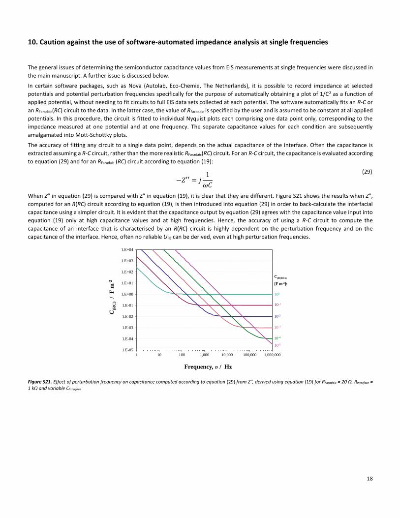
10. Caution against the use of software-automated impedance analysis at single frequencies
The general issues of determining the semiconductor capacitance values from EIS measurements at single frequencies were discussed in
the main manuscript. A further issue is discussed below.
In certain software packages, such as Nova (Autolab, Eco-Chemie, The Netherlands), it is possible to record impedance at selected
potentials and potential perturbation frequencies specifically for the purpose of automatically obtaining a plot of 1/C2 as a function of
applied potential, without needing to fit circuits to full EIS data sets collected at each potential. The software automatically fits an R-C or
an RFaradaic(RC) circuit to the data. In the latter case, the value of RFaradaic is specified by the user and is assumed to be constant at all applied
potentials. In this procedure, the circuit is fitted to individual Nyquist plots each comprising one data point only, corresponding to the
impedance measured at one potential and at one frequency. The separate capacitance values for each condition are subsequently
amalgamated into Mott-Schottky plots.
The accuracy of fitting any circuit to a single data point, depends on the actual capacitance of the interface. Often the capacitance is
extracted assuming a R-C circuit, rather than the more realistic RFaradaic(RC) circuit. For an R-C circuit, the capacitance is evaluated according
to equation (29) and for an RFaradaic (RC) circuit according to equation (19):
−𝑍′′ = 𝑗1
𝜔𝐶
(29)
When Z″ in equation (29) is compared with Z″ in equation (19), it is clear that they are different. Figure S21 shows the results when Z″,
computed for an R(RC) circuit according to equation (19), is then introduced into equation (29) in order to back-calculate the interfacial
capacitance using a simpler circuit. It is evident that the capacitance output by equation (29) agrees with the capacitance value input into
equation (19) only at high capacitance values and at high frequencies. Hence, the accuracy of using a R-C circuit to compute the
capacitance of an interface that is characterised by an R(RC) circuit is highly dependent on the perturbation frequency and on the
capacitance of the interface. Hence, often no reliable UFB can be derived, even at high perturbation frequencies.
Figure S21. Effect of perturbation frequency on capacitance computed according to equation (29) from Z″, derived using equation (19) for RFaradaic = 20 Ω, RInterface = 1 kΩ and variable CInterface
1.E-05
1.E-04
1.E-03
1.E-02
1.E-01
1.E+00
1.E+01
1.E+02
1.E+03
1.E+04
1 10 100 1,000 10,000 100,000 1,000,000
C(R
C)
/ F
m-2
Frequency, υ / Hz
C(R(RC))
[F m-2]:
10-5
10-4
10-3
10-2
10-1
100

19
11. α-Fe2O3 characterisation by X-ray photoelectron spectroscopy (XPS)
The surface of the Fe2O3 film was characterised using XPS (Thermo Scientific K-Alpha+ X-ray Photoelectron Spectrometer) operating at 2 ×
10−9 mbar base pressure. This system incorporated a monochromated, microfocused Al Kα X-ray source (hν = 1486.6 eV) and a 180° double
focusing hemispherical analyser with a 2D detector. The X-ray source was operated at a 6 mA emission current and 12 kV anode bias. Data
were collected at 200 eV pass energy for survey and 20 eV pass energy for core level spectra with a 400 μm2 X-ray beam. A flood gun was
used to minimize sample charging. All data were analysed using the Avantage software package. Core levels, shown in Figure S22 (a), were
confirmed to be characteristic of Fe2O3 and were in excellent agreement with measurements on undoped Fe2O3 that was produced by
magnetron sputtering specifically for XPS studies.19 A very small shoulder between ca. 806 and 809 eV, marked with an asterisk, is indicative
of a degree of Fe2+ polaron presence.19 The valence band maximum was determined to be 1.54 eV below the Fermi level, from fit to cut-off
of valence band feature in XPS, as shown in Figure S22 (b).
The purpose of this measurement was to determine the energy separation between the conduction band and Fermi level of our n-type Fe2O3,
which was calculated to be 0.56 eV if the electronic band gap is assumed to be the same as the optical band gap of 2.1 eV. This implies that
the conduction band potential of our samples lay 0.56 V negative of the determined flat band potentials. If that were so, hematite would
spontaneously evolve hydrogen. Furthermore, if the density of states in the conduction band, NC, is assumed to be in the range 4.6 × 1025 –
1.2 × 1026 m-3, as computed previously20, the separation of 0.56 eV would correspond to a bulk electron density, no, in the range 1.6 × 10¹⁶ –
4.2 × 10¹⁶ m-3. Such low electron densities are inconsistent with the measurements presented in this study.
(a) b)
(c)
Figure S22. (a) Fe 2p spectra and (b) valence band maximum energy of α-Fe2O3 film on FTO, measured using XPS; (c) the resultant position of the Fermi level relative to band edges and polaron level, arising from Fe2+ ions (polaron level was plotted using data from reference 19).
Fe3+ + e- ⟶ Fe2+
E–
E VB
M/
eV
Valence band
Conduction band
EF
[Ref 19]
[This work]
2.4
2.2
2.0
1.8
1.6
1.4
1.6
1.0
0.8
0.6
0.4
0.2
0
≈ 0.21 eV
EF
–E V
BM
= 1.
54 e
V
E vs Evac-4.2
-4.4
-4.6
-4.8
-5.0
-5.2
-5.4
-5.6
-5.8
-6.0
-6.2
-6.4
-6.6
EF ≈ -5.1 eV
EVBM ≈ -6.6 eV [Ref 19]
ECBM ≈ -4.4 eV [Ref 19]
20
However, if the reported electronic band gap of 1.75 eV19 is assumed, the energy separation between the conduction band and Fermi
level may be calculated as 0.21 eV, which is in much better, though not complete, agreement with our experimental observations. It is not
conclusive whether the small amount of Fe2+ polarons can be responsible for Fermi level pinning and the decrease in the electronic band gap
in hematite relative to the optical band gap. The presence of additional capacitance, observed at low frequencies in our EIS spectra, and the
Fermi level pinning observed in our OCP measurements, support the hypothesis of the influence of the Fe2+ polaron. The MS, GB and CI
methods of flat band potential determination support the new electron affinity, shown in Figure S22 (c) as it helps to explain why the flat
band potentials we determined were more negative than expected. It is currently unclear how the Fe2+ polaron formed on our samples and
how the conduction band and the polaron level can affect the various measurements differently. The solution is beyond the scope of this
study; hence, more detailed XPS investigations, accompanied by assessment of how electrochemical measurements may impact defect
formation, are required in the future to elucidate this.
12. References
1. Pleskov, Y. V.; Ya. Gurevich, Y., Semiconductor Photoelectrochemistry. Consultants Bureau: New York, 1986. 2. Gärtner, W. W., Depletion-Layer Photoeffects in Semiconductors. Physical Review 1959, 116 (1), 84-87. 3. Butler, M. A., Photoelectrolysis and physical properties of the semiconducting electrode WO2 Journal of Applied Physics 1977, 48 (5), 1914-1920. 4. Hankin, A.; Bedoya-Lora, F. E.; Ong, C. K.; Alexander, J. C.; Petter, F.; Kelsall, G. H., From millimetres to metres: the critical role of current density distributions in photo-electrochemical
reactor design. Energy & Environmental Science 2017, 10 (1), 346-360. 5. Cesar, I.; Sivula, K.; Kay, A.; Zboril, R.; Grätzel, M., Influence of Feature Size, Film Thickness, and Silicon Doping on the Performance of Nanostructured Hematite Photoanodes for Solar
Water Splitting. The Journal of Physical Chemistry C 2009, 113 (2), 772-782. 6. Le Formal, F.; Tétreault, N.; Cornuz, M.; Moehl, T.; Grätzel, M.; Sivula, K., Passivating surface states on water splitting hematite photoanodes with alumina overlayers. Chemical Science
2011, 2 (4), 737-743. 7. Klahr, B.; Gimenez, S.; Fabregat-Santiago, F.; Hamann, T.; Bisquert, J., Water Oxidation at Hematite Photoelectrodes: The Role of Surface States. Journal of the American Chemical
Society 2012, 134 (9), 4294-4302. 8. Dare-Edwards, M. P.; Goodenough, J. B.; Hamnett, A.; Trevellick, P. R., Electrochemistry and photoelectrochemistry of iron(III) oxide. Journal of the Chemical Society, Faraday
Transactions 1: Physical Chemistry in Condensed Phases 1983, 79 (9), 2027-2041. 9. Finklea, H. O., Semiconductor electrodes. Amsterdam, New York, Elsevier, 1988. 10. Schefold, J., Impedance and intensity modulated photocurrent spectroscopy as complementary differential methods in photoelectrochemistry. Journal of Electroanalytical Chemistry
1992, 341 (1), 111-136. 11. Harrington, S. P.; Devine, T. M., Analysis of Electrodes Displaying Frequency Dispersion in Mott-Schottky Tests. Journal of The Electrochemical Society 2008, 155 (8), C381-C386. 12. Bedoya, F. E.; Gallego, L. M.; Bermúdez, A.; Castaño, J. G.; Echeverría, F.; Calderón, J. A.; Maya, J. G., New strategy to assess the performance of organic coatings during ultraviolet–
condensation weathering tests. Electrochimica Acta 2014, 124, 119-127. 13. CALDERÓN-GUTIERREZ, J. A.; BEDOYA-LORA, F. E., BARRIER PROPERTY DETERMINATION AND LIFETIME PREDICTION BY ELECTROCHEMICAL IMPEDANCE SPECTROSCOPY OF A HIGH
PERFORMANCE ORGANIC COATING. DYNA 2014, 81, 97-106. 14. Hsu, C. H.; Mansfeld, F., Technical Note: Concerning the Conversion of the Constant Phase Element Parameter Y0 into a Capacitance. NACE-01090747 2001, 57 (09), 2. 15. Wan, T. H.; Saccoccio, M.; Chen, C.; Ciucci, F., Influence of the Discretization Methods on the Distribution of Relaxation Times Deconvolution: Implementing Radial Basis Functions with
DRTtools. Electrochimica Acta 2015, 184, 483-499. 16. Ciucci, F.; Chen, C., Analysis of Electrochemical Impedance Spectroscopy Data Using the Distribution of Relaxation Times: A Bayesian and Hierarchical Bayesian Approach.
Electrochimica Acta 2015, 167, 439-454. 17. Klotz, D.; Schmidt, J. P.; Kromp, A.; Weber, A.; Ivers-Tiffée, E., The Distribution of Relaxation Times as Beneficial Tool for Equivalent Circuit Modeling of Fuel Cells and Batteries. ECS
Transactions 2012, 41 (28), 25-33. 18. DRTTOOLS. https://sites.google.com/site/drttools/ (accessed 04/02/2019). 19. Lohaus, C.; Klein, A.; Jaegermann, W., Limitation of Fermi level shifts by polaron defect states in hematite photoelectrodes. Nature Communications 2018, 9 (1), 4309. 20. Hankin, A.; Alexander, J. C.; Kelsall, G. H., Constraints to the flat band potential of hematite photo-electrodes. Physical Chemistry Chemical Physics 2014, 16 (30), 16176-16186.