Embed Size (px)
Citation preview
Electronic devices and circuits
UNIT – I
PN- DIODE
04/18/23 www.noteshit.com 1
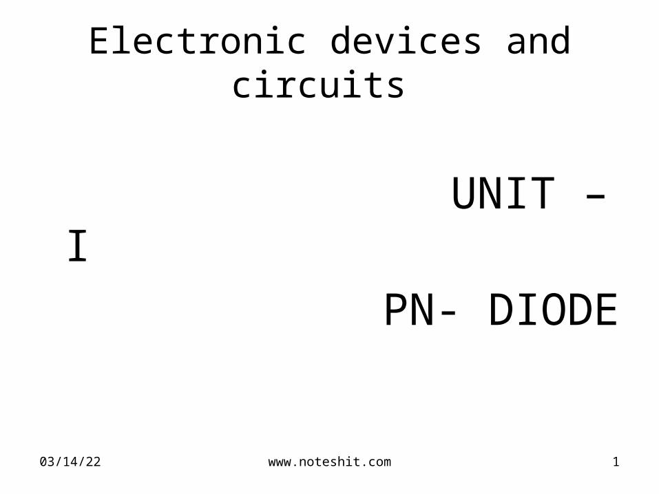
SEMICONDUCTOR DIODE
• Theory of p-n junction • p-n junction as diode • p-n diode currents • Volt-amp characteristics • Diode resistance • Temperature effect of p-n junction • Transition and diffusion capacitance of p-n
diode • Diode switching times
04/18/23 www.noteshit.com 2
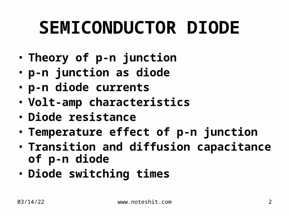
Theory of p-n junction
• When a p-type semiconductor material is suitably joined to n-type semiconductor the contact surface is called a p-n junction.
• P N+ +
Depletion region
04/18/23 www.noteshit.com 3
p-n junction as diode
• The p-n junction is also called as semiconductor diode .
• The left side material is a p-type semiconductor having –ve acceptor ions and +vely charged holes. The right side material is n-type semiconductor having +ve donor ions and free electrons
04/18/23 www.noteshit.com 4
p-n junction as diode
• Suppose the two pieces are suitably treated to form pn junction, then there is a tendency for the free electrons from n-type to diffuse over to the p-side and holes from p-type to the n-side . This process is called diffusion
The left side material is a p-type semiconductor having –ve acceptor ions and +vely charged holes. The right side material is n-type semiconductor having +ve donor ions and free electrons.
04/18/23 www.noteshit.com 5
p-n junction as diode
As the free electrons move across the junction from n-type to p-type, +ve donor ions are uncovered. Hence a +ve charge is built on the n-side of the junction. At the same time, the free electrons cross the junction and uncover the –ve acceptor ions by filling in the holes. Therefore a net –ve charge is established on p-side of the junction.
04/18/23 www.noteshit.com 6
p-n junction as diode
• When a sufficient number of donor and acceptor ions is uncovered further diffusion is prevented.
• Thus a barrier is set up against further movement of charge carriers. This is called potential barrier or junction barrier Vo. The potential barrier is of the order of 0.1 to 0.3V.
• Note: outside this barrier on each side of the junction, the material is still neutral. Only inside the barrier, there is a +ve charge on n-side and –ve charge on p-side. This region is called depletion layer.
04/18/23 www.noteshit.com 7
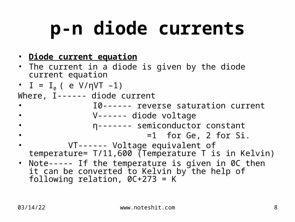
p-n diode currents• Diode current equation• The current in a diode is given by the diode current equation• I = I0 ( e V/ηVT –1)Where, I------ diode current• I0------ reverse saturation current• V------ diode voltage• η------- semiconductor constant• =1 for Ge, 2 for Si.• VT------ Voltage equivalent of temperature= T/11,600
(Temperature T is in Kelvin)• Note----- If the temperature is given in 0C then it can be converted
to Kelvin by the help of following relation, 0C+273 = K
04/18/23 www.noteshit.com 8
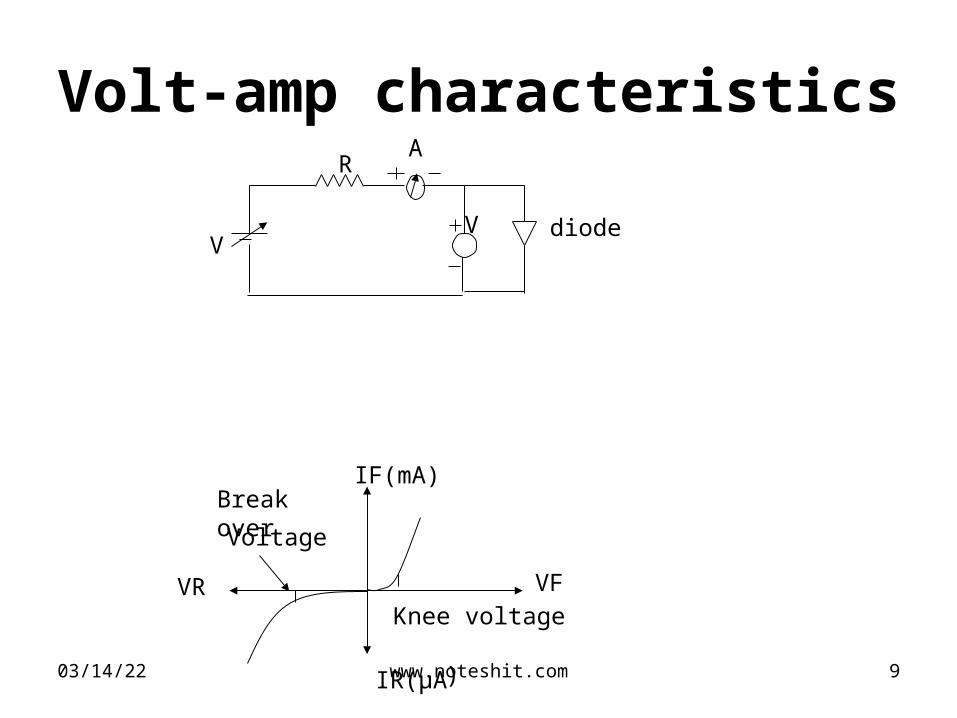
Volt-amp characteristics
R
A
V diode
VF
Knee voltageVR
IR(μA )
IF(mA)Break over
Voltage
V
04/18/23 www.noteshit.com 9
Volt-amp characteristics
• The supply voltage V is a regulated power supply, the diode is forward biased in the circuit shown. The resistor R is a current limiting resistor. The voltage across the diode is measured with the help of voltmeter and the current is recorded using an ammeter.
• By varying the supply voltage different sets of voltage and currents are obtained. By plotting these values on a graph, the forward characteristics can be obtained. It can be noted from the graph the current remains zero till the diode voltage attains the barrier potential.
• For silicon diode, the barrier potential is 0.7 V and for Germanium diode, it is 0.3 V. The barrier potential is also called as knee voltage or cur-in voltage.
04/18/23 www.noteshit.com 10
Diode equivalent circuit
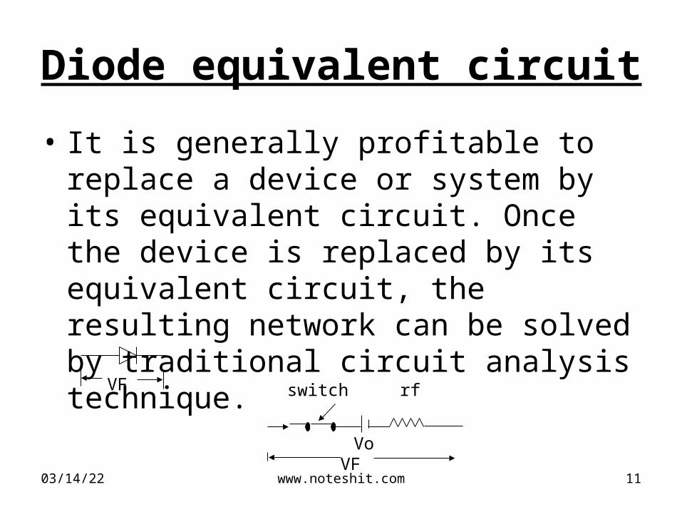
• It is generally profitable to replace a device or system by its equivalent circuit. Once the device is replaced by its equivalent circuit, the resulting network can be solved by traditional circuit analysis technique.
VF rf
Vo
switch
VF 04/18/23 www.noteshit.com 11
Diode resistance
• Static Resistance– Forward Resistance Rf
– Reverse Resistance Rr
• Dynamic Resistance– Forward Resistance rf
– Reverse Resistance rr
04/18/23 www.noteshit.com 12
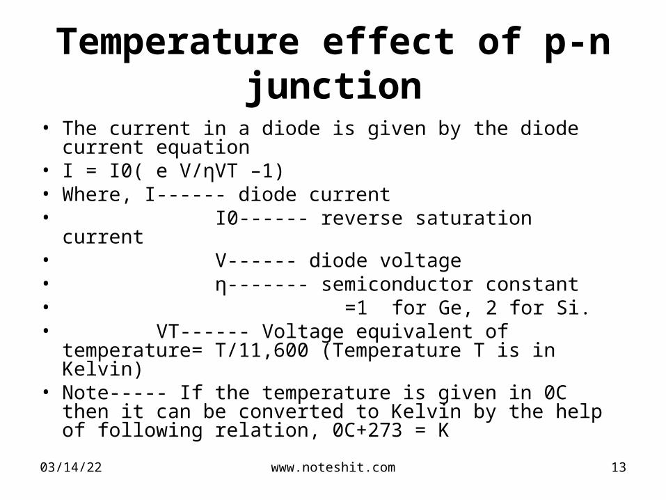
Temperature effect of p-n junction
• The current in a diode is given by the diode current equation
• I = I0( e V/ηVT –1)• Where, I------ diode current• I0------ reverse saturation current• V------ diode voltage• η------- semiconductor constant• =1 for Ge, 2 for Si.• VT------ Voltage equivalent of temperature=
T/11,600 (Temperature T is in Kelvin)• Note----- If the temperature is given in 0C then it can be
converted to Kelvin by the help of following relation, 0C+273 = K
04/18/23 www.noteshit.com 13
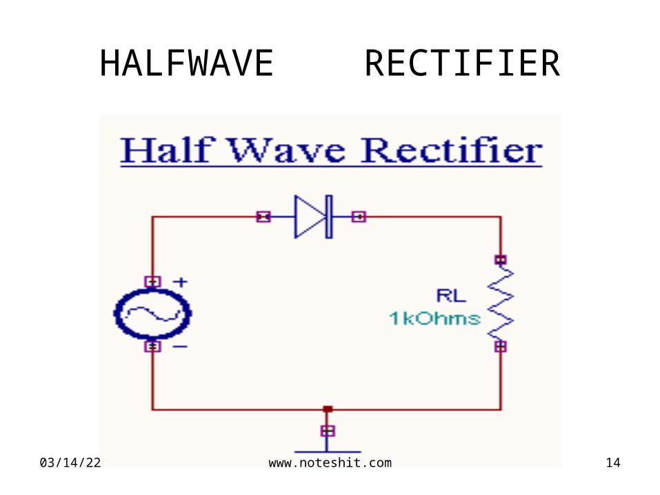
HALFWAVE RECTIFIER
04/18/23 www.noteshit.com 14
HALFWAVE RECTIFIER
• The primary of the transformer is connected to ac supply. This induces an ac voltage across the secondary of the transformer.
• During the positive half cycle of the input voltage the polarity of the voltage across the secondary forward biases the diode. As a result a current IL flows through the load resistor, RL. The forward biased diode offers a very low resistance and hence the voltage
04/18/23 www.noteshit.com 15
HALFWAVE RECTIFIER
• Drop across it is very small. Thus the voltage appearing across the load is practically the same as the input voltage at every instant.
• During the negative half cycle of the input voltage the polarity of the secondary voltage gets reversed. As a result, the diode is reverse biased.
• Practically no current flows through the circuit and almost no voltage is developed across the resistor. All input voltage appears across the diode itself.
04/18/23 www.noteshit.com 16
HALFWAVE RECTIFIER
• Hence we conclude that when the input voltage is going through its positive half cycle, output voltage is almost the same as the input voltage and during the negative half cycle no voltage is available across the load.
• This explains the unidirectional pulsating dc waveform obtained as output. The process of removing one half the input signal to establish a dc level is aptly called half wave rectification.
04/18/23 www.noteshit.com 17
HALFWAVE RECTIFIER
Peak Inverse Voltage
• When the input voltage reaches its maximum value Vm during the negative half cycle the voltage across the diode is also maximum. This maximum voltage is known as the peak inverse voltage.
Thus for a half wave rectifier Let Vi be the voltage to the primary of the
transformer. Vi is given by where Vr is the cut-in voltage of the diode.
04/18/23 www.noteshit.com 18
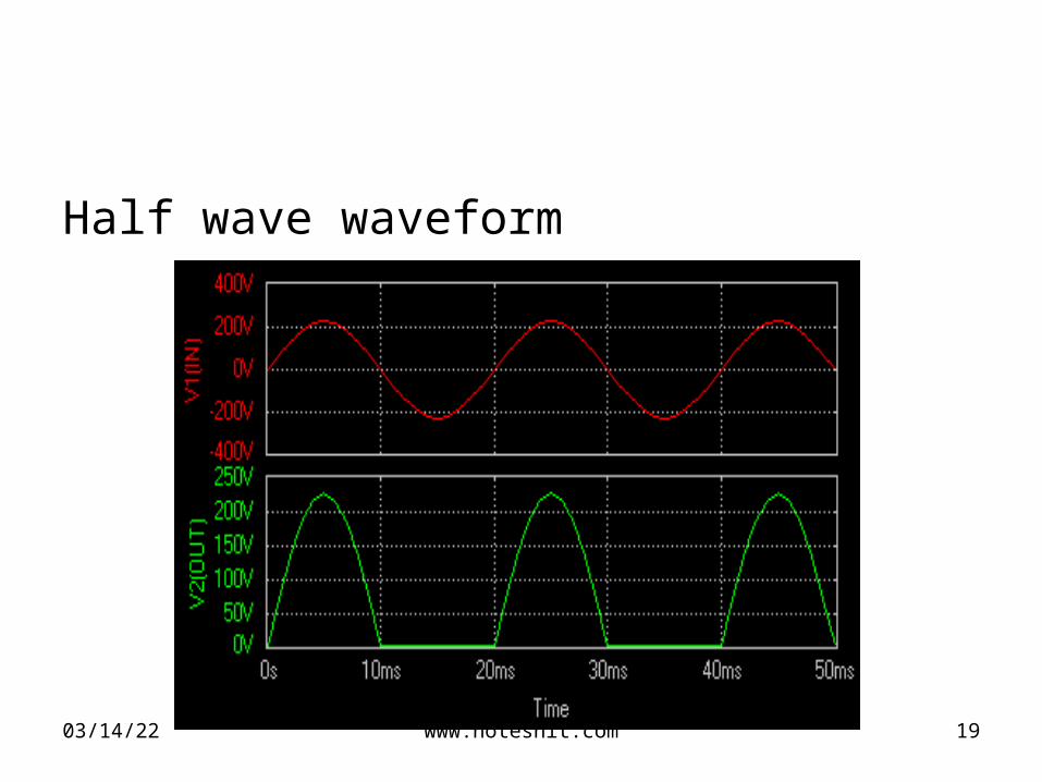
Half wave waveform
04/18/23 www.noteshit.com 19
HALFWAVE RECTIFIER
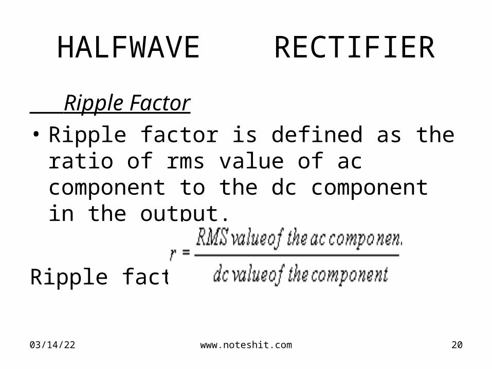
Ripple Factor
• Ripple factor is defined as the ratio of rms value of ac component to the dc component in the output.
Ripple factor
04/18/23 www.noteshit.com 20
HALFWAVE RECTIFIER
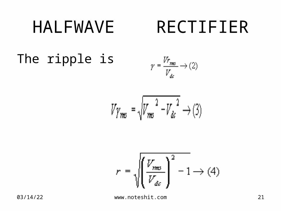
The ripple is
04/18/23 www.noteshit.com 21
HALFWAVE RECTIFIER
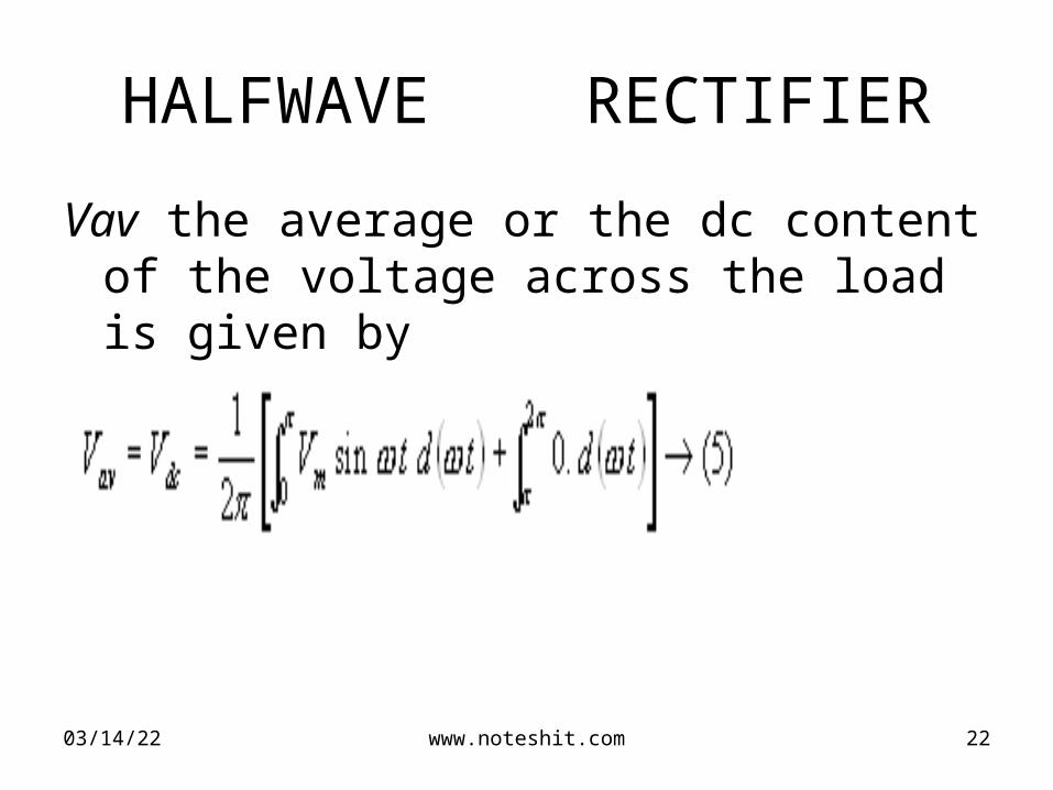
Vav the average or the dc content of the voltage across the load is given by
04/18/23 www.noteshit.com 22
HALFWAVE RECTIFIER
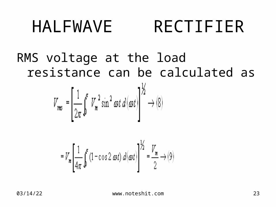
RMS voltage at the load resistance can be calculated as
04/18/23 www.noteshit.com 23
HALFWAVE RECTIFIER
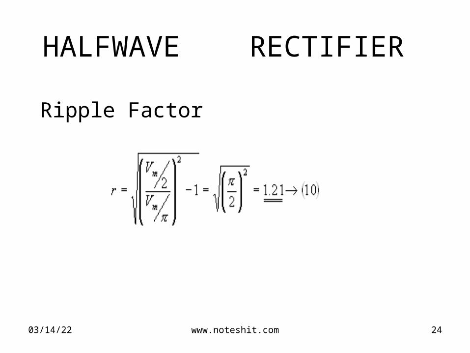
Ripple Factor
04/18/23 www.noteshit.com 24
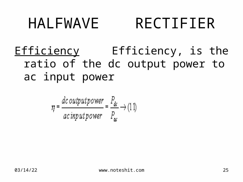
HALFWAVE RECTIFIER
Efficiency Efficiency, is the ratio of the dc output power to ac input power
04/18/23 www.noteshit.com 25
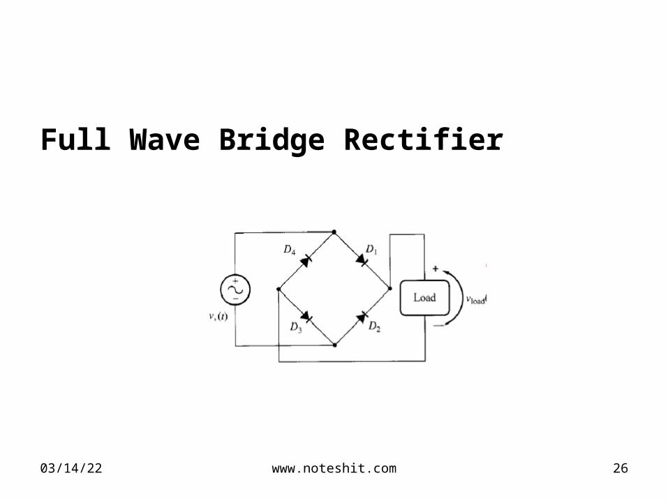
Full Wave Bridge Rectifier
04/18/23 www.noteshit.com 26
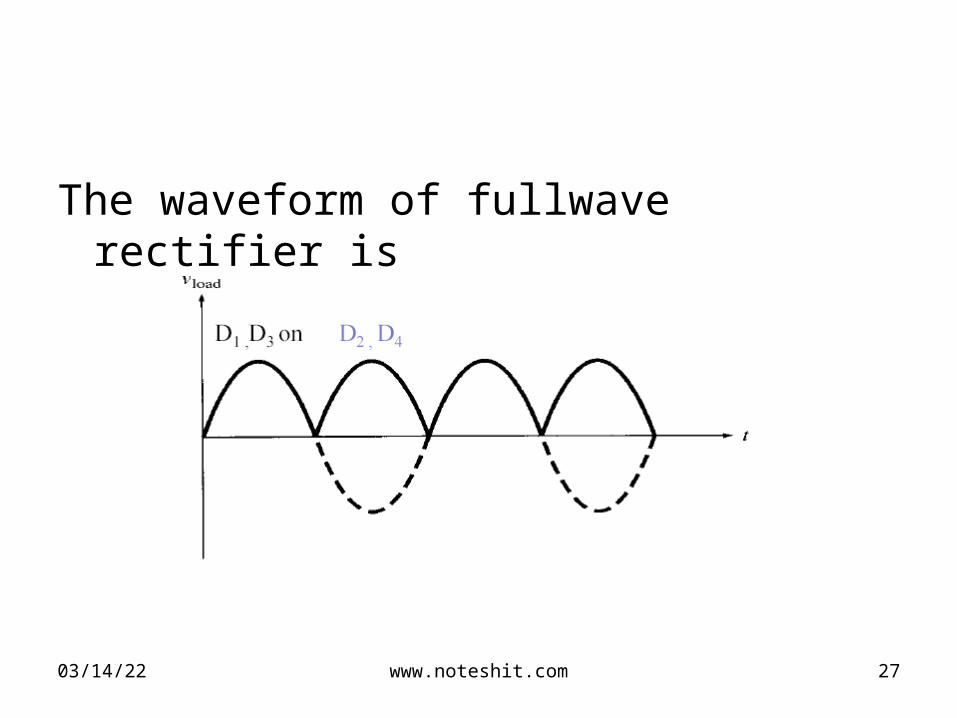
The waveform of fullwave rectifier is
04/18/23 www.noteshit.com 27
Zener Diode
• Zener Diode : Works in the break down region when subjected to reverse bias.
• Large variation in current. Voltage almost constant.
• Used for voltage regulation. Upper limit of current depends on the power dissipation rating of the device.
04/18/23 www.noteshit.com 28
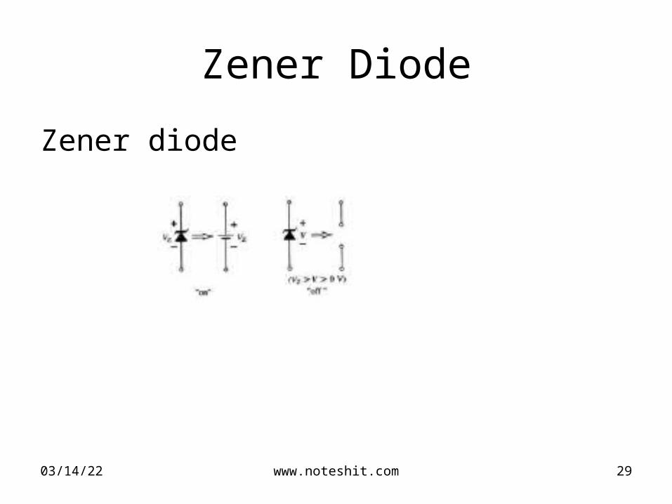
Zener Diode
Zener diode
04/18/23 www.noteshit.com 29
Light Emitting Diode
Light emitting diodes (LEDs)
• The Light Emitting Diode (LED) is a common light source used in electronic circuits.
• LED is a semiconductor diode that emits light when current passes through it.
04/18/23 www.noteshit.com 30
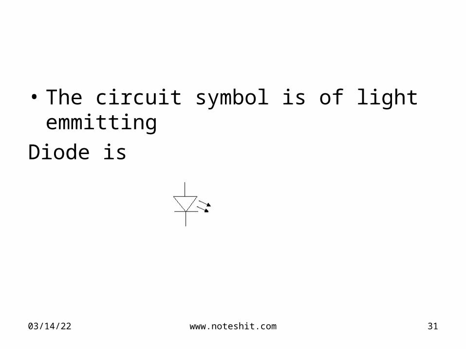
• The circuit symbol is of light emmitting
Diode is
04/18/23 www.noteshit.com 31
• The characteristics of the LED are similar to other semiconductor diodes except the operating
• voltage is higher.
• A typical LED has an operating voltage of 2.0V and a maximum current of 30mA.
04/18/23 www.noteshit.com 32
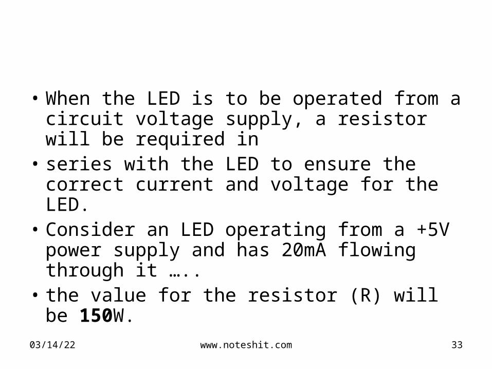
• When the LED is to be operated from a circuit voltage supply, a resistor will be required in
• series with the LED to ensure the correct current and voltage for the LED.
• Consider an LED operating from a +5V power supply and has 20mA flowing through it …..
• the value for the resistor (R) will be 150W.
04/18/23 www.noteshit.com 33
LIQUID CRYSTAL DISPLAY
LIQUID CRYSTAL DISPLAY - They are used for display of numeric and alphanumeric character in dot matrix and segmental display.
04/18/23 www.noteshit.com 34
• What is a Liquid Crystal?Liquid Crystal – a stable phase of matter
characterized by anisotropic properties without the existence of a 3-dimensional crystal lattice – generally lying between the solid and isotropic (“liquid”) phase.
04/18/23 www.noteshit.com 35
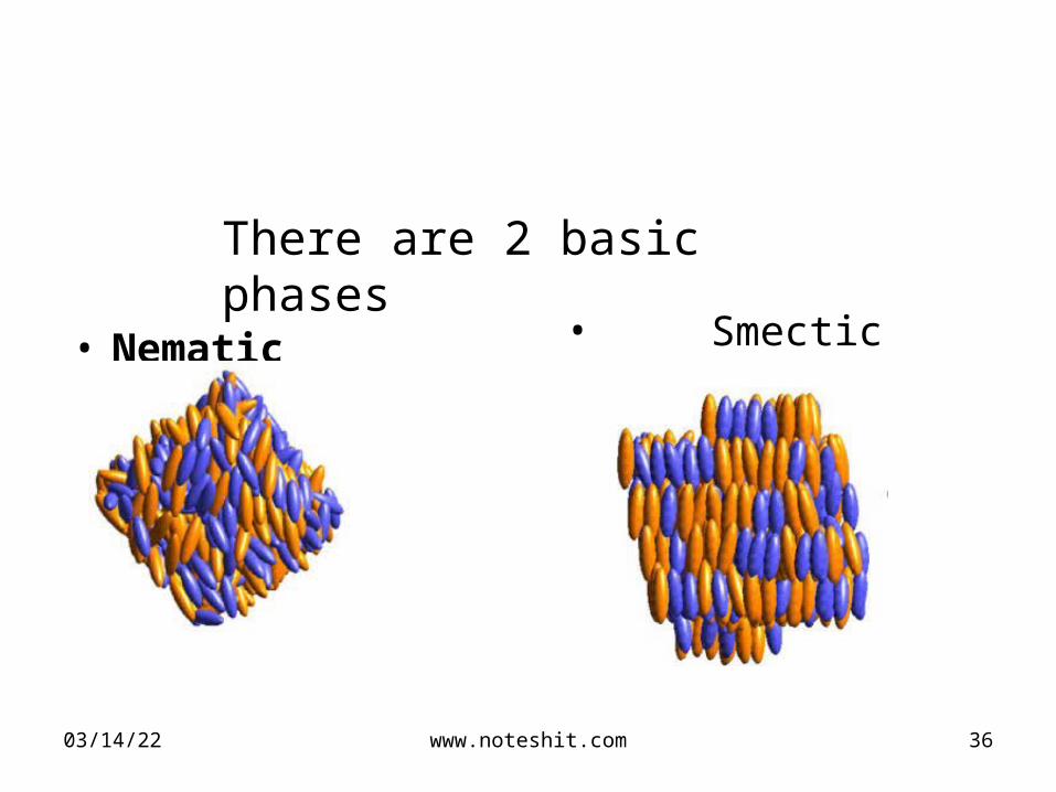
• Nematic
• Smectic
There are 2 basic phases
04/18/23 www.noteshit.com 36
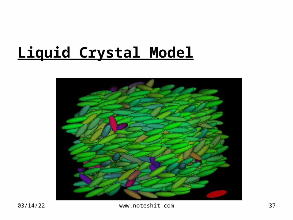
Liquid Crystal Model
04/18/23 www.noteshit.com 37
Series voltage regulator
In a voltage regulator circuit , if the control elements are connected in series with load it is called series voltage regulator .
04/18/23 www.noteshit.com 38
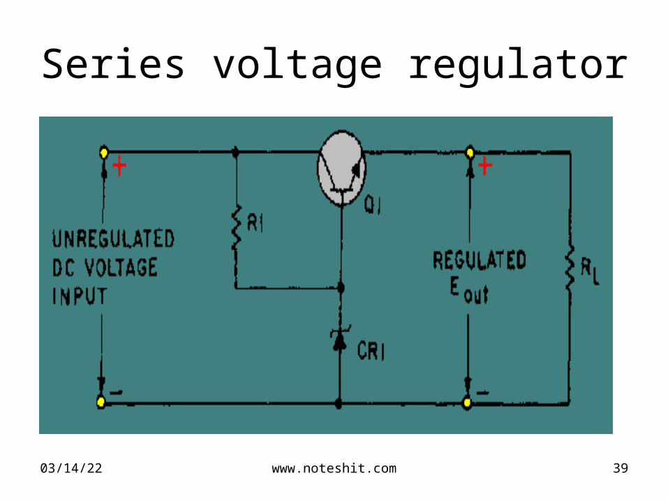
Series voltage regulator
04/18/23 www.noteshit.com 39
• Zener diode is a diode that block current until a specified voltage is applied. Remember also that the applied voltage is called the breakdown, or Zener voltage. Zener diodes are available with different Zener voltages. When the Zener voltage is reached, the Zener diode conducts from its anode to its cathode (with the direction of the arrow).
• In this voltage regulator, Q1 has a constant voltage applied to its base.
04/18/23 www.noteshit.com 40
This voltage is often called the reference voltage. As changes in the circuit output voltage occur, they are sensed at the emitter of Q1 producing a corresponding change in the forward bias of the transistor.
In other words, Q1 compensates by increasing or decreasing its resistance in order to change the circuit voltage division.
04/18/23 www.noteshit.com 41
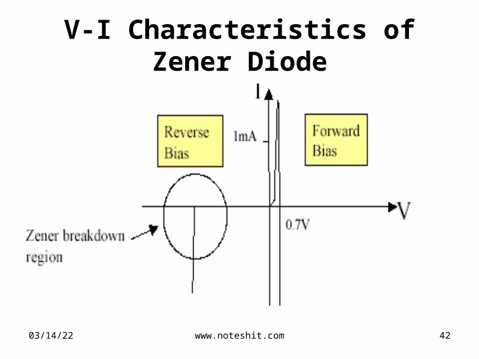
V-I Characteristics of Zener Diode
04/18/23 www.noteshit.com 42
V-I Characteristics of Zener Diode
• Zener diodes are manufactured to have a very low reverse bias breakdown voltage
• Since the breakdown at the zener voltage is so sharp, these devices are often used in voltage regulators to provide precise
voltage references. The actual zener voltage is device dependent. For example, you can buy a 6V zener diode.
04/18/23 www.noteshit.com 43
THANK U
04/18/23 www.noteshit.com 44

![Chapter 1: Diode circuits vtusolutionvtusolution.in/uploads/9/9/9/3/99939970/analog_electronic[15ec32].pdf · Chapter 1: Diode circuits ... • Diode testing • Zener diode • Diode](https://img.pdfslide.us/doc/110x75/5aedefea7f8b9a9031905d54/chapter-1-diode-circuits-vt-15ec32pdfchapter-1-diode-circuits-diode.jpg)

![$$ 5 - . 1 ) $ · ... PN junction, Junction Theory, VI characteristics of PN junction diode, Ideal diode, Static and Dynamic Resistance [1][2], Diode current equation[2],Diode notations](https://img.pdfslide.us/doc/110x75/5ae6f8997f8b9a29048e3147/-5-1-pn-junction-junction-theory-vi-characteristics-of-pn-junction.jpg)