Embed Size (px)
Citation preview

1
Electron spin
• Was first introduced in 1925 by Uhlenbeck and Goudsmit to explain the hyperfine structure of the atomic spectrum.
• A theoretical foundation has been provided in 1928 by Dirac by making a relativistic correction to the wave equation.
Spintronics
1. Explain what electron spin is. Introduce magnetoresistance. Give example of magnetoresistance in a material or system. What
is role of electron spin in magnetoresistance of materials? What is spintronics?

2
Discovery of electron spinThe discovery note in Naturwissenschaften is dated Saturday 17 October 1925. One day earlier Ehrenfest had written to Lorentz to make an appointment for the coming Monday to discuss a "very witty idea" of two of his graduate students. When Lorentz pointed out that the idea of a spinning electron would be incompatible with classical electrodynamics, Uhlenbeck asked Ehrenfest not to submit the paper. Ehrenfestreplied that he had already sent off their note, and he added: "You are both young enough to be able to afford a stupidity!"
Ehrenfest's encouraging response to his students ideas contrasted sharply with that of Wolfgang Pauli. As it turned out, Ralph Kronig, a young Columbia University PhD who had spent two years studying in Europe, had come up with the idea of electron spin several months before Uhlenbeck and Goudsmit. He had put it before Pauli for his reactions, who had ridiculed it, saying that "it is indeed very clever but of course has nothing to do with reality". Kronig did not publish his ideas on spin. No wonder that Uhlenbeck would later refer to the "luck and privilege to be students of Paul Ehrenfest".
Spintronics
(left) and (right) proposed the idea that each electron spins with an angular momentum of one half Planck constant and carries a magnetic moment of one Bohr magneton (1925).

Spintronics
•Spintronics investigates control and manipulation of the electron spin in metals and semiconductors.
•Anisotropic magnetoresistance effect (AMR) was used in the magnetic read heads of earlier generations.
•In nanostructures spin polarization of the current adds a dramatic new functionality establishing polarization-based electronic circuits in addition to charge-based circuits.
•Current and future applications range from spin-based field effect transistors (FETs), through permanent magnetic storage devices without moving parts like read/write heads, to quantum computers.
•Due to much larger scattering length, spin is superior to charge in terms of coherent effects and for quantum computation applications.
SpintronicsConferences
People
2. Give examples of spintronics applications. What is spintronics advantage comparable with conventional (charge) electronics?
Why could spin be more effective than charge?

4
Taking magnetism for a
spin: Exploring the
mysteries of skyrmions23 January 2019, by Laura Millsaps
2019 highlights
Skyrmions are nanoscale whirls or
vortices of magnetic poles that form
lattices within a magnetic material, a
type of quasiparticle that can zip across
the material, pushed by electrical
current. Credit: Ames Laboratory, US
Department of Energy
Retrieved 11 March 2019 from https://phys.org/news/2019-01-magnetism-exploring-mysteriesskyrmions.html

5
Relaxation Dynamics of Zero-Field Skyrmions over a
Wide Temperature Range
Nano Lett. 2018, 18, 7777−7783
The promise of magnetic skyrmions in future spintronic devices
hinges on their topologically enhanced stability and the ability to be
manipulated by external fields. The technological advantages of
nonvolatile zero-field skyrmion lattice (SkL) are significant if their
stability and reliability can be demonstrated over a broad temperature
range. Here, we study the relaxation dynamics including the evolution
and lifetime of zero-field skyrmions generated from field cooling (FC) in
an FeGe single-crystal plate via in situ Lorentz transmission electron
microscopy (L-TEM). Three types of dynamic switching between zero-
field skyrmions and stripes are identified and distinguished.

6
New quantum system could help design better spintronics
2019 highlights
Purdue University researchers used lasers to trap and cool
atoms down to nearly absolute zero, at which point they
become a quantum fluid known as Bose-Einstein
condensate, and collided condensates with opposite spins.
Credit: Purdue Quantum Center
Retrieved 11 March 2019 from https://phys.org/news/2019-01-quantum-spintronics.html
Laser cooling technologies won
the Nobel Prize in physics in 1997.
Inside the mini quantum fluid
collider, Chen's team sent two
BECs with opposite spins
smashing into one another.
Like two clouds of gas would,
they partially penetrate each
other, delivering a spin current.
Using this system, researchers
can literally turn spin-orbit
coupling on and off, which
allows them to isolate its effect
on spin current decay. This
can't be done with electrons in
solid-state materials, which is
part of what makes this system
so powerful.
29 January 2019

7
Electronics of the future: A new energy efficient
mechanism using the Rashba effect
~2019 highlight
A new mechanism to generate a spin current without energy loss from a series of simulations for
new bismuth-adsorbed indium based quasi-1-D materials that exhibit a giant Rashba effect is
proposed. The mechanism is suitable for spintronic applications, having the advantage that it does
not require an external magnetic field to generate nondissipative spin current.
Retrieved 11 March 2019 from https://phys.org/news/2018-12-electronics-future-energyefficient-mechanism-rashba.html
28 December 2018

8
Toward ultrafast spintronics
2019 highlights
An ultrashort pulse of spin current, lasting less than a picosecond (one trillionth of a second), can be
injected from a metal to a semiconductor with amazing efficiency, breaking the previous spin injection
record by over 10000 times. Ultrashort spin current pulses are produced by shining a laser pulse on cobalt,
a magnetic metal. This generates a swarm of excited electrons with spin polarisation, meaning that the
spins mostly point in the same direction. The spin carrying electrons then travel outward, diffusing into
other adjacent materials.
Retrieved 11 March 2019 from https://phys.org/news/2019-01-ultrafast-spintronics.html
Schematic
of the spin-
injection
experiment.
Credit: J. C.
W. Song
and Y. D.
Chong
21 January 2019

9
Laser pulses light the way to tuning topological
materials for spintronics and quantum computing
2019 highlights
Three-dimensional topological
insulators are emerging materials
that hold great promise due to their
unique electron conducting states
on their surfaces, immune to
backscattering, versus the bulk
interior, which behaves as a normal
insulator.
By employing ultra-short mid-
infrared and terahertz pulses of
less than one trillionth of a second,
researchers at Ames Laboratory
were able to successfully isolate
and control the surface properties
of a bismuth-selenium (Bi2Se3) 3-D
topological insulator.
Retrieved 11 March 2019 from https://phys.org/news/2019-02-quantum-computinghow-electrons.html
Credit: Ames Laboratory
15 February 2019

10
Engineers develop room temperature, two dimensional
platform for quantum technology
2019 highlights
Researchers at the University of Pennsylvania's School of Engineering and
Applied Science have now demonstrated a new hardware platform based
on isolated electron spins in a two-dimensional material. The electrons are
trapped by defects in sheets of hexagonal boron nitride, a one-atom-thick
semiconductor material, and the researchers were able to optically detect
the system's quantum states. Credit: Ann Sizemore Blevins
Retrieved 11 March 2019 from https://phys.org/news/2019-02-room-temperature-twodimensional-platform-quantum.html
11 February 2019

11
Spontaneous spin polarization demonstrated in a two-
dimensional material
2019 highlights
In a two-dimensional layer of molybdenum disulfide, the electron-electron
interaction (blue threads) force the spins of the electrons (violet spheres) to
align. Credit: Department of Physics, University of Basel
Retrieved 11 March 2019 from https://phys.org/news/2019-03-spontaneous-polarization-twodimensional-material.html
11 March 2019

12
Magnonic devices can replace electronics
without much noise
2019 highlights
Chip that generates a magnonic current, or spin wave, between transmitting
and receiving antennae. Credit: Balandin Lab at UC Riverside
Retrieved 11 March 2019 from https://phys.org/news/2019-03-magnonic-devices-electronics-noise.html
4 March 2019,
by Holly Ober

13
Magnetoresistance (MR) is the change of resistance of a conductor in an external magnetic field.
In typical metal, at room temperature, orbital MR effects are very small, at most of the order of a few per cent.
Comment: For a spherically-symmetric energy spectrum
Therefore, the xx-component is field-independent. However, energy spectrum of realistic metals is anisotropic.
Magnetoresistance
Spintronics
3. Is orbital magnetoresistance large in typical metals at room temperature? How does xx component of longitudinal resistance
depend on field in two-dimensional electron gas? Can you derive its value from the conductance matrix?

Update of solid state physics 14
Diffusive transport
Between scattering events electrons move like free particles with a given effective mass.
In 1D case the relation between the final velocity and the
effective free path, l, is then
Assuming where is the drift velocitywhile is the typical velocity and introducing the collision time as we obtain in the linear approximation:
Mobility

Update of solid state physics 15
In magnetic field
“friction” Lorentz force
Diffusion motion of electron in magnetic field
ωcτ ≤ 1

Update of solid state physics 16
Conductivity tensor
Magnetic field is applied in the z-direction, B = (0, 0, B)
Here vi are the components of the drift velocity vector. Solving this systemof equations for j gives j = σE with
Important quantity is the product of the cyclotron frequency, by the relaxation time,
Resistivity (inverse to conductivity) tensor:
^ conductivity as a tensor,
S is a geometry factor

Giant magnetoresistance 17
Magnetic field on nanoscale
It is not difficult to get large fields going to nanometer scale.

Giant magnetoresistance 18
The MR effect has been of substantial importance technologically, especially in connection with read-out heads for magnetic disks and as sensors of magnetic fields. The most useful material has been an alloy between iron and nickel, Fe20Ni80 (permalloy).
The general consensus in the 1980s was that it was not possible to
significantly improve performance of magnetic sensors based on MR.
Closed orbits: B-independent
resistance
Open orbits: MR ~ B2
Magnetoresistance in bulk

Giant magnetoresistance 19
Tunneling magnetoresistance
4. Introduce effect of tunnelling magnetoresistance (TMR). What are the materials suitable for tunnelling magnetoresistance devices?
Explain how TMR works and how to make tunnel magnetoresistance junctions. What are current and expected applications of TMR?
By Fred the OysteriThe source code of this SVG is valid.This vector graphics image was created with Adobe Illustrator., GFDL, https://commons.wikimedia.org/w/index.php?curid=36210012
‘Tunnel magnetoresistance (TMR) is a magnetoresistive effect that occurs in a magnetic
tunnel junction (MTJ), which is a component consisting of two ferromagnets separated
by a thin insulator.’
https://en.wikipedia.org/wiki/Tunnel_magnetoresistance
‘The effect was originally discovered in 1975 by M.
Jullière (University of Rennes, France) in Fe/Ge-O/Co-
junctions at 4.2 K. The relative change of resistance
was around 14%, and did not attract much attention. In
1991 Terunobu Miyazaki (Tohoku University, Japan)
found an effect of 2.7% at room temperature. Later, in
1994, Miyazaki found 18% in junctions of iron separated
by an amorphous aluminum oxide insulator and
Jagadeesh Moodera found 11.8% in junctions with
electrodes of CoFe and Co. The highest effects
observed to date with aluminum oxide insulators are
around 70% at room temperature.’

Giant magnetoresistance 20
Here the insulator should be only a few atomic layers thick so that there is a significant probability that electrons can quantum mechanically tunnel through the
insulating barrier
Fe/amorphous Ge/Co, Ni/NiO/(Fe,Co,Ni),
CoFe / Al2O3 /Co, Fe /Al2O3/ Fe,
Fe/MgO/Fe – TMR can exceed 200%
Due to the better performance of the magnetic tunnel junctions they are expected to become the material of choice for technical applications.
Their use for non-volatile magnetic random access memories (MRAM) is of particular interest - MRAM systems based on TMR are already on the market.
One expects that TMR based technologies will become dominant over the GMR sensors.
Tunneling magnetoresistance
4. Introduce effect of tunnelling magnetoresistance (TMR). What are the materials suitable for tunnelling magnetoresistance devices?
Explain how TMR works and how to make tunnel magnetoresistance junctions. What are current and expected applications of TMR?

21
Spin interacts only weakly with its environment. The majority of the electron scattering events are spin-conserving, and it can therefore be expected that spin is conserved over distances that are much larger than the elastic mean free path. Key parameter in spintronics is spin polarization which could be defined as:
↑ and ↓ denote the majority and the minority spin, respectively. For q↓ = 0, polarization Pq = 1; while for q↓ = q↑, Pq = 0.
TMR refers to the resistance of a ferromagnet–insulator–ferromagnet (FIF) tunnel junction in which coercive magnetic fields differ by a significant amount, which allows the relative orientation of the magnetizations to be changed by sweeping a magnetic field aligned parallel to the layers. It was found that, for the magnetizations of the two layers aligned parallel to each other, the tunnel resistance is lower than for antiparallel alignment.
Spin polarization
Spintronics
5. What is spin polarization? Write its expression. What is effect of spin polarization on tunnelling magnetoresistance? Is tunnel
resistance lower for antiparallel alignment of spins?

22
Magneto-resistance of a TMRstructure formed by a CoFe–Al2O3–Co sandwich, with themagnetization directions of thetwo films as indicated in theschemes (bottom) Also shown inthe top two traces are the muchweaker anisotropic magneto-resistances of the correspondingindividual films.
The tunnel resistance is lower for parallel alignment.
Effect of spin polarization
Spintronics
‘The upper two curves show the small
magnetoresistance changes in the two
films (not the junction) which mark the
coercive fields (Hc) by the position of
their extrema. (The presence of a
maximum or minimum is determined
by the field and current directions.)’

23
We define conductances Gp and Gap for the parallel and antiparallelconfigurations. The densities of states for the source and drainferromagnetic electrodes are labeled D↑(↓)S and D↑(↓)D.
Conductance and polarization
Since, in a ferromagnet, D↑ > D↓, we have Gp > Gap.
The tunneling magnetoresistance (TMR) is usually defined as:Here Rap,p denotes the resistance of the correspondingconfigurations.Inserting the conductances gives:Here P denotes the polarizationof the density of states. In cobalt, for example, PCo = 0.34,which gives a TMR of 0.26 in an ideal system.
Spintronics
6. Link conductance and polarization. How is tunnelling magnetoresistance (define it) expressed through the polarization of source
and drain? Give an example of ideal TMR value for a metal, for instance, cobalt.
24
In a magnetic random access memory (MRAM) chip, each bit is stored in a sequenceof TMR layers. The lower ferromagnetic layer is hard, i.e. not reversible by themagnetic fields acting on the layers. The spin state of upper layer can be changed bycurrent.
TMR in memory chips
The memory can be read out without a magnetic read head. Two states of the bitcorrespond to the two values of the measured current through tunnel junction. Nomoving parts are required. The stored data does not get lost when the power isturned off.
The square arrays of TMR columns arecontacted by one-dimensional arrays ofwires on the top and on the bottom, whichare rotated by 90◦ with respect to eachother. In this way, each element of thearray can be addressed individually. Thewriting, which means defining theorientation of the top magnetic layer, canbe done by current pulses.
Spintronics
7. Explain how tunnelling magnetoresistance can be used in memory chips? Is hard ferromagnetic layer necessary
in their construction? Is yes, why? How to assemble a sequence of TMR elements and how to write and read
information? Are movable parts necessary? Are stored data lost when the power is turned off?

25
TMR based memory chips
Spintronics
Dynamic random-access memory
Static random-access memory

Giant magnetoresistance 26
In GMR, as in TMR resistance depends on the relative orientation of the magnetizations of the ferromagnetic layers. Replace the insulator in a TMR layer sequence by a normal metal, and you have a GMR structure. It has been established that resistance dependence originates mostly from spin-dependent transmission of the conduction electrons across the ferromagnet–normal metal interfaces.
Giant magnetoresistance
8. Introduce phenomenon of giant magnetoresistance (GMR). In what systems does it take place? What are materials suitable for
GMR devices and how are they used? What is the difference between GMR and TMR?
Giant magnetoresistance 27
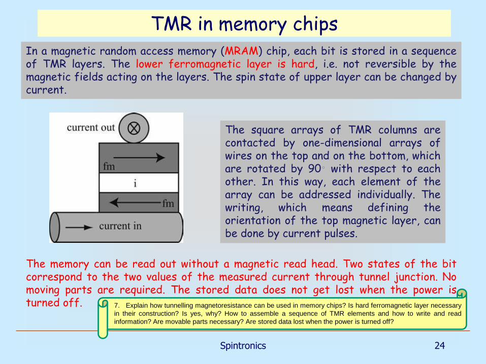
Fe/Cr/Fe trilayer, P. Grünberg, room temperature
(FeCr)n, n=60. A. Fert,
Liquid He temperature
Giant magnetoresistance structures

Giant magnetoresistance 28
Giant magnetoresistance: two-current model
The GMR effect asobserved on a Fe–Cr–Fesandwich structure. Theanisotropic magneto-resistance of aferromagnetic thin film isshown in comparison.
Mott’s two-current model
In the parallel configuration,the highly transmissive spinchannel dominates theresistance; whereas, in theantiparallel configuration,both spin channelscontribute equally to theresistance. This results in alower overall resistance forthe parallel configuration.
8. Introduce phenomenon of giant magnetoresistance (GMR). In what systems
does it take place? What are materials suitable for GMR devices and how are
they used? What is the difference between GMR and TMR?

Giant magnetoresistance 29
Non-magnetic state:
numbers of spin-up and spin-down electrons are
equal
Ferromagnetic state:
numbers of spin-up and spin-down electrons are
different
Density of states (DOS) profile

Giant magnetoresistance 30
Antiferromagnettrilayer system, H=0
Shown are DOS for up-and down- spins
Equivalent circuit diagram
Magnetic field aligns the magnetic moments of the layers
Physics of GMR
12. Explain physics of GMR introducing equivalent circuit diagrams. What is the difference in resistance between parallel and
antiparallel orientations? Is any way to enhance GMR using half-metals?

Giant magnetoresistance31
Ferromagnet trilayersystem, H≠0
Shown are DOS for up-and down- spins
Difference
Spin aligned layers

Giant magnetoresistance 32
A way to enhance GMR: Half-metals
We are interested in the largest possible difference in the Fermi-level DOS for spin up and spin down.
In half-metals the spin down band is metallic while the spin up band is
an insulator (example – CrO2).
Magnetic stateNon-magnetic state

Giant magnetoresistance 33
No electric current (spin blockade)
Only spin down current
Half-metals GMR

Giant magnetoresistance 34
3d transition metals - Fe, Co, Ni; lantanides (4f) - Gd
The origin of magnetism - behavior of the 3d/4f electrons, respectively. We will focus on 3d elements.
In the free atoms, the 3d and 4s levels of the 3d transition elements are hosts for the valence electrons.
In the metallic state these 3d and 4s levels are broadened into energy bands.
4s orbitals are rather extended overlap between 4s orbitals of neighboring atoms 4s band is spread out over a wide energy
range (15–20 eV).
3d orbitals are much less extended in space associated 3d
energy band is comparatively narrow (4–7 eV).
4s electrons are much more mobile than 3d ones.
Ferromagnetic metals
11. How do different spin states influence resistance of a material? How do 4d-electron states contribute to the resistance? What are requirements
for building magnetic superlattices for GMR devices? How to engineer magnetic materials using principle of Friedel oscillations? How do electrons
in non-magnetic layers provide coupling between magnetic layers?

Giant magnetoresistance 35
Energy of the state depends on the interplay between the (exchange) interaction between electrons and their kinetic energy.
The Exchange Interaction:arises from Coulomb electrostatic interaction andthe Pauli exclusion principle
Higher repulsion energy Lower repulsion energy
Lowering energy of the state

Giant magnetoresistance 36
Exchange interaction requires overlap of wave functions.
Exchange interaction
Giant magnetoresistance 37
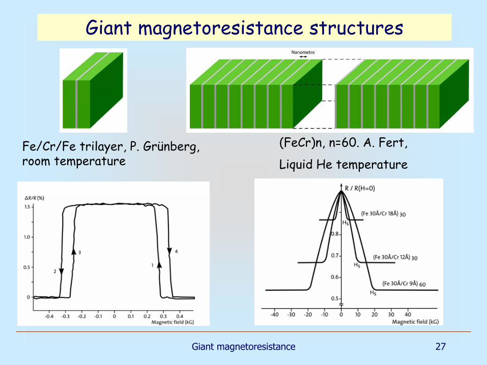
Imperfections (defects and impurities) in metals become screened by the surrounding conduction electrons.
The imperfection gives rise to decaying (Friedel) oscillations of the
electron density as a function of the distance from the disruption.
Similarly, a magnetic impurity atom in a metal gives rise to an induced spin polarization of the electron density.
With increasing distance from the magnetic impurity there will be an oscillation in the sign of the polarization and the disturbance will also decay in magnitude with distance.
As a consequence, the magnetic moment of a second impurity will become aligned parallel or antiparallel to the magnetic moment of the first moment depending on the sign of the induced polarization at that
particular distance.
Magnetic impurities
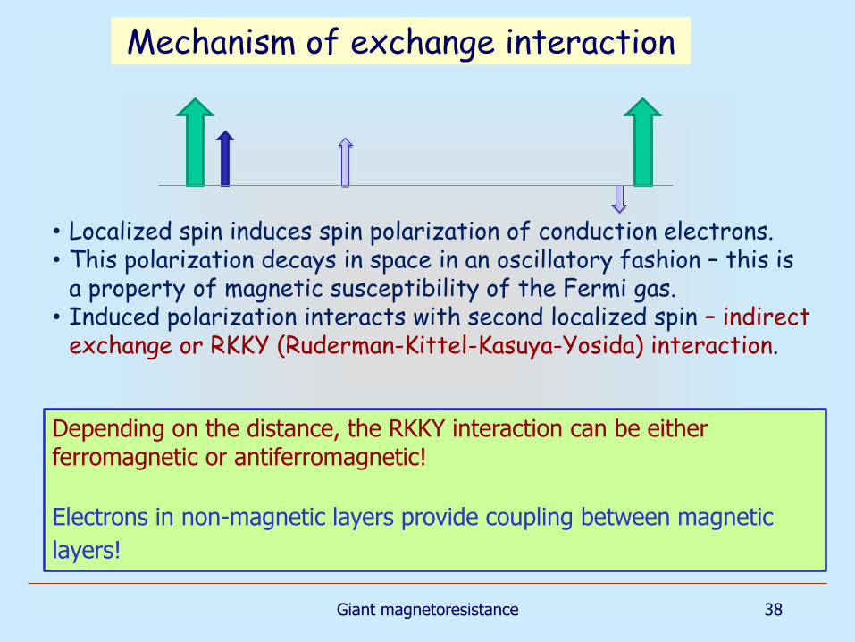
Giant magnetoresistance 38
• Localized spin induces spin polarization of conduction electrons.• This polarization decays in space in an oscillatory fashion – this is
a property of magnetic susceptibility of the Fermi gas.• Induced polarization interacts with second localized spin – indirect
exchange or RKKY (Ruderman-Kittel-Kasuya-Yosida) interaction.
Depending on the distance, the RKKY interaction can be either ferromagnetic or antiferromagnetic!
Electrons in non-magnetic layers provide coupling between magnetic
layers!
Mechanism of exchange interaction

Giant magnetoresistance 39
How much does it cost to create a FM state?
A transfer of spin down electrons from the spin down band into the spin up band leads to lowering of the total energy (a gain).
On the other hand, such a process requires a transfer of electrons from spin down levels below the initial Fermi energy, into spin up levels situated just above the initial Fermi energy. That will increase the total energy (a loss).
Thus there is a competition between two opposite effects. This can be formulated as the so called Stoner criterion for ferromagnetism,
Here J is called the Stoner exchange parameter and N(EF) is the density of states at the Fermi energy.
J N (EF ) ¸ 1
Itinerant magnetism
10. Explain the concept of itinerant magnetism. Does itinerant magnetism important for giant magnetoresistance? In what materials
does it takes place and what orbitals are most important for this effect? What role does exchange interaction play in itinerant
magnetism? What is the Stoner criterion for ferromagnetism? Do you know a metal, which is on the verge of ferromagnetism?

Giant magnetoresistance 40
Resistivity for different spin states
Conductivity of d transition elements is mainly determined by the 4s electrons (easily mobile due to the wide 4s energy bands).
However s electrons can scatter into the many d states which are available at the Fermi level considerable resistance.
In a ferromagnet like Fe there are 2 types of carriers, one made up from spin up electrons and one from spin down electrons.
Since the density of states at the Fermi surface is quite different for the two spin states it follows that there is a significant difference in resistance for the spin up electrons and the spin down electrons.
For Cu (following Ni in the Periodic Table) all the 3d states are situated below the Fermi level and therefore not available for scattering processes. This explains the particularly high conductivity of Cu.
Sir Nevil Mott, 1936

Giant magnetoresistance 41
It is important that the lattice parameters for the different layers match each other; it is also an advantage if the two metals forming the superlattice have the same crystal structure.
This is the case for Cr and Fe, where both metals adapt the bcc crystal structure and have very similar
lattice spacing.
It was also extremely important that the spatial separation between the magnetic layers is of the order of nanometers.
In order to exhibit the GMR effect the mean free path for the conduction electrons has to greatly exceed the interlayer separationsso that the electrons can travel through magnetic layers and pick up
the GMR effect.
Magnetic superlattices

Giant magnetoresistance 42
MBE
Growth of metallic
multilayers
Key ingredients
Novel characterization
methods
At present time, GMR structures can be also obtained by magnetron sputtering
Preparation of superlattices

Giant magnetoresistance 43
A prerequisite for the discovery of the GMR-effect was provided by the new possibilities of producing fine layers of metals on the nanometer scale.
Originally, epitaxy was used. At present time, after Stuart Parkin, more simple and cheap method – sputtering – is more practical.
GMR effect and applications
GMR effect can also be observed when the current flows parallel to the layers. One speaks of the current perpendicular to plane (CPP) and the current in plane (CIP) configurations. In spite being much weaker, CIP isan important configuration, since CPP has very small overall resistance.
13. Can GMR effect be observed when the current flows parallel to the layers? Explain physics of it. What are current-
perpendicular-to-plane (CPP) and the current-in-plane (CIP) configurations? Why is CIP important?

Giant magnetoresistance 44
The current density across the interface between a ferromagnet (F)and a normal conductor (N), is composed of two spin components, j = j↑+ j↓. The spin current density is given by js = j↑ − j↓. Here, we denoteby ↑ the majority spin in the ferromagnet. In a normal conductor,there is no spin current associated with a charge current.
Spin injection
βN is the fraction of the current density carried by the spin-up channelin the normal metal.
In the centre of normal conductor:
Close to interface:
14. Outline principles of spin injection. Describe spin transport in ferromagnet and spin accumulation close to interface with normal
metal. Introduce spin-flip scattering time and spin relaxation length. Describe these processes in specific materials.

Giant magnetoresistance 45
Spin injection: spin transport in ferromagnet
Here βF is the fraction of the current density carried by the spin-up channel in the ferromagnet.
Here denote the spin-resolved densities of states at the Fermi energy and the diffusion constants, respectively, while αF
represents the fraction of the total ferromagnet conductance that is contributed by the spin up channel.
The current in ferromagnet is split among the spin channels:
In the ferromagnet, the two spin directions experience different conductivities:
Because in the normal metal, spin channels have equal conductances and in ferromagnet not, the spin accumulates close to the interface, and a spin density gradient builds up in both materials. This means that, in the interface region, the two spin directions have different electrochemicalPotentials with and .

Giant magnetoresistance 46
Spin injection: diffusion equation
Here λF(N) is the spin relaxation length in the corresponding material.
Here nF↑(↓) denotes the spin-resolved electron densities, T↑↓ (T↓↑) are the spin-flip scattering times from ↑ into ↓ (respectively, from ↓ into ↑) and T1F
is the spin relaxation time
By introducing spin-flip scattering times:
the diffusion equation can be obtained
Diffusion equation:
Diffusion equation solution:

Giant magnetoresistance 47
Spin injection: properties of interface
For a ferromagnet with PjF = 1, the spins are perfectly injected into the normal metal! To aim for a large spin polarization in the normal conductor, (λN/σN)/(λF/σF) should be as small as possible.
Spin accumulation at theferromagnet–normal metalinterface, expressed interms of the spin-resolvedelectrochemical potentials.The step of the averagedelectrochemical potentialsacross the interface isdenoted by Δμ.
By solving current equations on both sides of interface and equalling currents, one can obtain:
15. How are chemical potentials of differently polarized electrons linked in the interface? Write expression for the current
polarization at an ferromagnet-normal metal interface. What is the condition of perfect injection of spins?

48
Spin injection: experiments
A spin-polarized current is injected from permalloy (Ni80Fe20)into copper, and a value of Pj,Cu = 0.02 was extracted. A spin-flip time T1,Cu of 42 ps was found at 4.2K, which corresponds toλCu ≈ 1 μm. Since the Drude scattering time in copper is 30 fsat 4.2K, these results show that the electrons experience1000 elastic scattering events on average before theyexperience a spin flip. Even at room temperature, a relativelylarge value of λCu ≈ 350 nm remains.
Spintronics

‘Colossal magnetoresistance (CMR) is a property of some materials, mostly
manganese-based perovskite oxides, that enables them to dramatically
change their electrical resistance in the presence of a magnetic field. The
magnetoresistance of conventional materials enables changes in resistance of
up to 5%, but materials featuring CMR may demonstrate resistance changes
by orders of magnitude. This technology may find uses in disk read-and-write
heads, allowing for increases in hard disk drive data density.’
Colossal magnetoresistance
La0.67Ca0.33MnO3 La0.67Sr0.33MnO3
TCurie = 250 K TCurie = 350 K
CMR materials are perovskites
with crystal lattice that is very
close to crystal lattice of high-
temperature superconductors,
for example, YBa2Cu3Ox.
Y Tokura, Critical features of colossal magnetoresistive manganites, Reports on
Progress in Physics, Volume 69, Number 3 , p. 797–851 (2006).

I
CMR
HTS
1
4
3
5
2
H
1 - STO substrate (5 mm 5 mm);
2 - YBCO; 3 - STO barrier; 4 -
CMR; 5 - gold contact pads. The
arrow shows the direction of the
applied field.
EF
Spin injection into YBa2Cu3Ox

Current dependence of the effect of spin
injection
0 2 4 64
5
6
7
8
I = 0 - 61.6 mA
m (
10
-8 A
m2)
t (min.)
10
20
30
40
50
60
1
3
4
5
5
6
7
8
9
m (
10
-8
Am
2
)
0I (mA)t (
min
.)
p=1 s

0 50 100 150 200 250 3000.0
0.2
0.4
0.6
0.8
1.0
1.2
1.4
1.6
1.8
2.0 350, 3 h 350, 3 h 350 C, 10 h 350-270 C, 24 h 350-270 C, 24 h 350-270 C, 48 h 350-270 C, 96 h
R /
R2
90
K
T (K)
-600 -400 -200 0 200 400 600 800 1000
0.9985
0.9990
0.9995
1.0000
1.0005 18.8 K 68.9 K 73.5 K 78.3 K 87.4 K 89.2 K135.0 K 144.6 K
C8_9
R/R
0
H (Oe)
0 50 100 150 200 250 3002
4
6
8
10
12
14
16
0 50 100 150 200 250 300
0.0
0.5
1.0
1.5
2.0
R (
Oh
m)
T (K)
YBCO
Au
YBCO
YBCO/LCMO&Au interfaceAu
V1
I1
V2
I2
Interaction with antiferromagnetic spin
fluctuations: annealing experiments
The annealing experiments, which change T* and the upper boundary of AFM spin
fluctuations, display the removal of increase in resistance and coercive field effect. 0 50 100 150 200 250 300
0.0
0.5
1.0
1.5
2.0
2.5
YBCO/LCMO
Am
plitu
de
(1
0-2 a
.u.)
T (K)
As prepared
Exposed,7 months
TCurie
Annealed

Spin injection into ultrathing films
I1 V1 V2 I2
I1 I2 V1 V2 Au
YBa2Cu3Ox
La0.7Ca0.3MnO3
SrTiO3 substrate -15 -10 -5 0 5 10 15
-2.0
-1.5
-1.0
-0.5
0.0
0.5
1.0
1.5
2.0
72.2 K
I (m
A)
V (mV)
59.8 K
The bilayer is set in the
resistive state
Quasiparticle exchange has a considerable ab-plane component
YBCO film:
12-25 nm
I1 V1 V2 I2

10 20 30 40 50 60 70 80-1
0
1
2
3
4
5
6
7
8
Data: EffectPercent_B
Model: Gauss
Equation: y=y0 + (A/(w*sqrt(PI/2)))*exp(-2*((x-xc)/w)^2)
Weighting:
y No weighting
Chi^2/DoF = 0.46578
R^2 = 0.91036
y0 0 ±0
xc1 -126.12913 ±447.91613
w1 131.93271 ±190.65388
A1 8578.91865 ±80400.10215
xc2 73.95354 ±1.19084
w2 3.43068 ±3.21179
A2 4.08436 ±4.01884
V
(%
)
T (K)
Spin injection into ultrathing films
-500 -400 -300 -200 -100 0 100 200 300 400
5.00
5.05
5.10
5.15
5.20
5.25
5.30
5.35
72.7 K
V (
10
-4 V
)
H (a.u.)
74.7 K
78.4 K
40 50 60 70 80 90 100 110 120 130 140
0
2
4
6
8
10
12
14
R (
Ohm
)
T (K)
YBCO
d = 25 nm
Minimums dissapear here Both low-temperature and close-to-Tc effects of spin
injection are observed in ultrathing films
-400 -200 0 200 400 600
-0.0016
-0.0008
0.0000
0.0008
0.0016
m (
A m
2)
H (Oe)

4-corners transport measurements
0 50 100 150 200 250 300
5
10
15
20
25
Temperature (K)
Re
sis
tan
ce
(
)
Re
sis
tan
ce
(
)
Temperature (K)
0.1 V 1.8 V
0.3 V 5.0 V
50 60 70 80 90
5
10
15
20
25
I
VV
I
Montgomery technique

Superconductivity: seeing is believing
Faraday effect and magneto-optical imaging
The Faraday effect is a rotation of
the polarization of light in
presence of magnetic field. The
effect was discovered by Michael
Faraday in 1845.
Michael Faraday, 1842, by Thomas Phillips
https://en.wikipedia.org/wiki/Michael_Faraday

Magneto-optical study
A differential MOI image showing the in- plane magnetization of the LCMO thin film surface. The
sample is covered with an MO-indicator film and the red line indicates where the sample ends. The
contrast in the image represents areas of strong and weak magnetic fields periodically alternating in
the plane of the film and seen as bright and dark areas, respectively.

Anisotropy transport measurements
, 10 - 15 September 2017, Zatoka, Ukraine
I
VV
I
20 40 60 80 100 120
0
500
1000
1500
2000
2500 parallel
perpendicular
Re
sis
tan
ce
(
Temperature (K)
40 50 60 70 800
20
40
60
Re
sis
tan
ce
(
Temperature (K)

Scanning electron microscopy and EDX
, 10 - 15 September 2017, Zatoka, Ukraine
Mn-KA 500 nm
500 nm
La0.67Ca0.33MnO
3
YBa2Cu3O7-d
500 nm
Scanning electron microscopy and EDX confirm presence of both layers with reasonably well
defined interface.

X-ray diffraction study
, 10 - 15 September 2017, Zatoka, Ukraine
The main peak in x-ray diffraction scan is from the SrTiO3-substrate. LCMO and YBCO are also
identified in the scan. In addition, there are some unknown peaks that indicate significant inter-
diffusion between the LCMO and YBCO forming interface layer with different properties than those
of the pure compounds.
20 40 60 80 100 120 140
10
100
1000
10000
100000
Unknown
phase
LCMO/
YBCO
log
10(i
nte
nsity [a
.u.]
)
Angle [degrees]
SrTiO3
Thickness fringe
110 112 114 116 118

0 50 100 150 200 250 300-9
-8
-7
-6
-5
-4
-3
-2
ZFCW 1 T
FCW 1 T
FCC 1 T
m (
10
-4 e
mu)
T(K)
Magnetization measurements

Interface magnetism
J. Chakhalian et al., Magnetism at the interface between ferromagnetic and
superconducting oxides, Nature Physics 2, 244 (2006).
‘Here we examine superlattices composed of the halfmetallic ferromagnet La2/3Ca1/3MnO3 and the high-
temperature superconductor YBa2Cu3O7 by absorption spectroscopy with circularly polarized X-rays and
by off-specular neutron reflectometry. The resulting data yield microscopic insight into the interplay of spin
and orbital degrees of freedom at the interface. The experiments also reveal an extensive rearrangement
of the magnetic domain structure at the superconducting transition temperature.’
‘Carefully controlled interfaces between two materials
can give rise to novel physical phenomena and
functionalities not exhibited by either of the constituent
materials alone.’

An ex-situ YBCO/LCMO bilayer was investigated by a range of
techniques.
A strong anisotropy in resistance and a resistance peak is
observed below critical temperature of superconductor.
The resistance peak corresponds to stripy magnetic structure
seen by magneto-optical imaging and registered by vibrating
sample magnetometry.
It is suggested that magnetic structure is associated with
YBCO/LCMO interface.
, 10 - 15 September 2017, Zatoka, Ukraine
Giant magnetoresistance 64
65 70 75 80 85 90 95 100
0,0
0,2
0,4
0,6
0,8
1,0
65 70 75 80 85 90 95 100
0,0
0,2
0,4
0,6
0,8
1,0
65 70 75 80 85 90 95 100
0,0
0,2
0,4
0,6
0,8
1,0
65 70 75 80 85 90 95 100
0,0
0,2
0,4
0,6
0,8
1,0
Spin Injection
No Spin Injection
Difference
R[O
hm
]
T[K]
1 V 3 V
Spin Injection
No Spin Injection
Difference
R[O
hm
]
T[K]
9 V
Spin Injection
No Spin Injection
Difference
R[O
hm
]
T[K]
15 V
Spin Injection
No Spin Injection
Difference
R[O
hm
]
T[K]
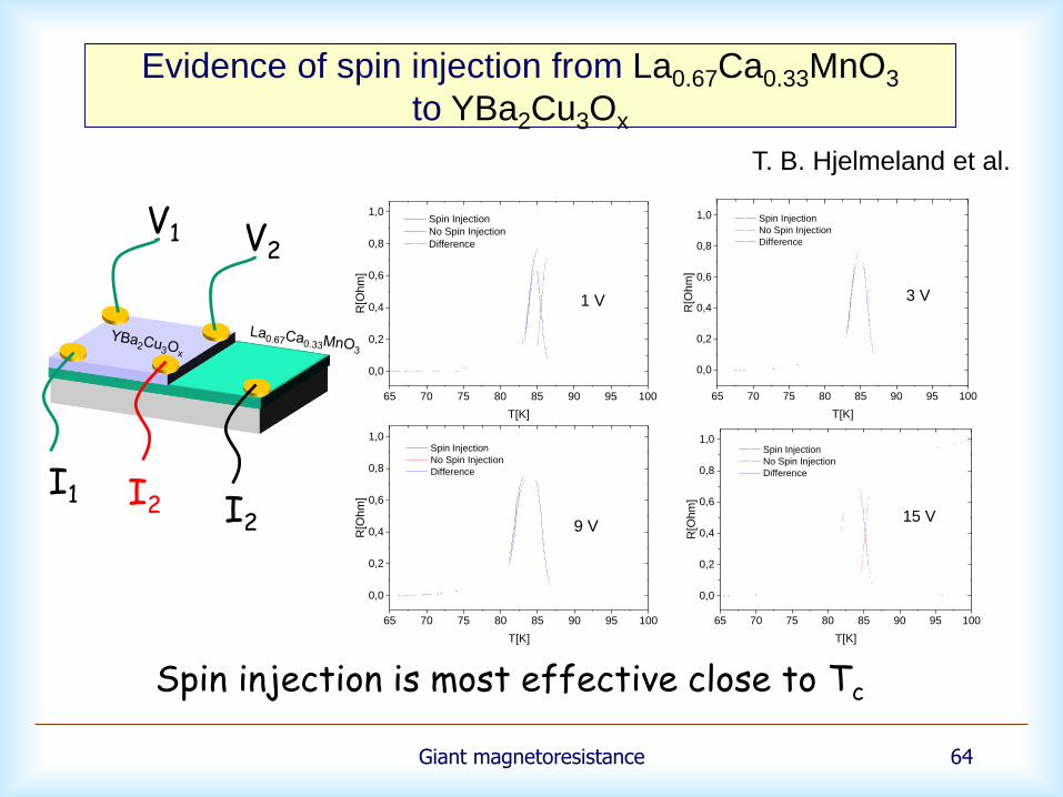
T. B. Hjelmeland et al.
Evidence of spin injection from La0.67Ca0.33MnO3
to YBa2Cu3Ox
Spin injection is most effective close to Tc
V1
I2 I2
V2
I1

0 50 100 150 200 250 300
0
500
1000
1500
2000
0 50 100 150 200 250 3000,000
0,002
0,004
0,006
0,008
0,010
0,012
0,014
0,016
R (
Oh
m)
T (K)
1 V
3 V
6 V
9 V
12 V
15 VI
[A]
T [K]
Giant magnetoresistance 65
T. B. Hjelmeland et al.
Evidence of spin injection from La0.67Ca0.33MnO3
to YBa2Cu3Ox
V1
I2
V2
I1
50 100 150 200 250 300-2
0
2
4
6
8
10
12
14
R (
Ohm
)
T (K)
1 V
3 V
6 V
9 V
12 V
15 V
Spin injection in normal state of YBa2Cu3Ox is revealed.
V2
V2
V2

Giant magnetoresistance 66
T. B. Hjelmeland et al.
Evidence of spin injection from La0.67Ca0.33MnO3
to YBa2Cu3Ox
Spin injection in normal state of YBa2Cu3Ox is revealed.
V1
I2 I2
V2
I1
50 100 150 200 250 300-2
0
2
4
6
8
10
12
14
R (
Ohm
)
T (K)
1 V
3 V
6 V
9 V
12 V
15 V
100 150 200 250 300
-0,2
0,0
0,2
0,4
0,6
R(O
hm
)
T(K)
1 V
1 V
3 V
3 V
9 V
9 V
15 V
15 V
YBCO LCMO
YBCO
Straight line is subtracted, two measurement configurations

Spintronics 67
Datta–Das spin transistor
Spin-polarized electrons are injected in the semiconductor
Gate is used to rotate the polarization plane (Rashba effect)
Ferromagnetic drain contact is used as analyzer
Idea by Datta & DasNot realized experimentally
No need to add/remove electrons – less energy
consumption!
S. Datta and B. Das, Appl. Phys. Lett. 56, 665 (1990)
Spin FET is a modification of a GMR structure.
16. Introduce concept of Datta–Das spin transistor. Is it implemented? Does it use semiconductor? What are difficulties in
injecting spins into semiconductor and what are possible solutions to overcome these difficulties? How can additional interface
resistance in a tunnel barrier structure increase injected spin polarization?

Giant magnetoresistance 68
Spin injection into semiconductors
Additional interface resistance Ri↑(↓) depends on spin and makes the spin-resolved electrochemical potentials discontinuous at the interface.
Two possible solutions: a) a ferromagnet with a spin polarization of PjF = 1,b) inserting tunnel barriers at the ferromagnet–semiconductor interfaceto use spin-selective interface resistance.
It is difficult task becauseconductivity is lower than thatof the ferromagnet and thespin-flip length is longer.
Interface tunnel barriers
Giant magnetoresistance 69
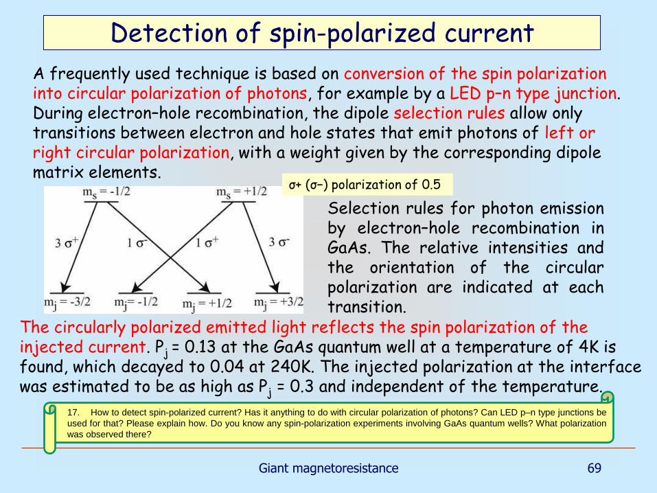
Detection of spin-polarized current
The circularly polarized emitted light reflects the spin polarization of the injected current. Pj = 0.13 at the GaAs quantum well at a temperature of 4K is found, which decayed to 0.04 at 240K. The injected polarization at the interface was estimated to be as high as Pj = 0.3 and independent of the temperature.
A frequently used technique is based on conversion of the spin polarization into circular polarization of photons, for example by a LED p–n type junction. During electron–hole recombination, the dipole selection rules allow only transitions between electron and hole states that emit photons of left or right circular polarization, with a weight given by the corresponding dipole matrix elements.
Selection rules for photon emissionby electron–hole recombination inGaAs. The relative intensities andthe orientation of the circularpolarization are indicated at eachtransition.
σ+ (σ−) polarization of 0.5
17. How to detect spin-polarized current? Has it anything to do with circular polarization of photons? Can LED p–n type junctions be
used for that? Please explain how. Do you know any spin-polarization experiments involving GaAs quantum wells? What polarization
was observed there?

Giant magnetoresistance 70
Ferromagnetic semiconductors
A spin polarization of the current injected from Ga1−xMnxAs into GaAs of Pj = 0.82 at liquid helium temperatures has been found. The impedance mismatch problem has been solved, at least conceptually.
The Fermi energy in semiconductors is small compared to that in metals, and can become smaller than the spin splitting of the conduction band. This results in a spin polarization of 1. Consequently, the impedance mismatch problem would not occur.
Magnetization hysteresis curves of Ga1−xMnxAs.
The remanenceand the coercivemagnetic fieldcould be tuned bya gate voltage.
Spin injectionfrom aferromagneticsemiconductorinto a GaAsquantum well.
A significant circularpolarization of theemitted light isdetected.
18. What are ferromagnetic semiconductors? Do they help to solve the impedance mismatch problem? Can they have spin
polarization equal to 1? How it can be achieved? Can Ga1−xMnxAs be used as a ferromagnetic semiconductor? What are the results
of experiments with this compound?

71
Due to the band offsets at the interface of two different materials the electrons are confined in a quantum well. A two-dimensional electron gas (2DEG) is formed. If the potential well is asymmetric, the electrons are moving in an effective electric field E. In the reference system of the electron this electrical field transforms into a magnetic field B. Depending of the spin orientation and the corresponding magnetic moment an energy lowering or an energy increase occurs, respectively. For applications it is essential, that the strength of the Rashba effect and thus the spin splitting can be controlled by means of a gate electrode.
Rashba effect
Spintronics
The Rashba effect denotes the spin–orbit coupling experienced by moving electrons in electric fields. It can be induced by macroscopic electric field in a semiconductor quantum well.
19. What is Rashba effect? Can you explain its origin? Do you know any experimental observations of the Rashba effect? How could
this effect be used in spin based field-effect transistor? What are the conditions for constructing Datta–Das transistor?

72
The Rashba effect is a direct result of inversion symmetry breaking in the direction perpendicular to the two-dimensional plane. Therefore, let us add to the Hamiltonian a term that breaks this symmetry in the form of an electric field
Due to relativistic corrections an electron moving with velocity v in the electric field will experience an effective magnetic field B
This magnetic field couples to the electron spin
where is the magnetic moment of the electron.
Within this toy model, the Rashba Hamiltonian is given by:
Derivation of Rashba effect
Spintronics
The energy dispersion of afree 2DEG in an In0.53Ga0.47As–In0.52Al0.48As quantum well withη = 10−11 eV m and m∗ ≈ 0.05me,with the Rashba effect takeninto account. The arrows depictthe corresponding spindirections.The eigenvalues are:

73
This is a rotation along a circle formed by the intersection of the Bloch sphere with the planegiven by φ. In real space, the spinor rotates around the direction of the magnetic field seenby the electron, i.e. around the axis in the (x, y) plane that is perpendicular to k. For theabove values, we find from ΔkFL = 2 a rotation about over a distance L.
Observation of Rashba effect
Spintronics
For a Fermi energy of EF = 10 meV and aspin–orbit coupling constant η = 10−11 eV m,we find ΔkF = 1.7×10⁷m−1 ≈ 0.13kF. Itcorresponds to a modulation of certainwavelength.
Modulation of Shubnikov–de Haasoscillations due to the Rashba effect.
The Datta–Das transistor only works when the spin directions are well defined,which means that the channel should be quasi-one-dimensional. Second, thechannel should be ballistic. Even though elastic scattering does not flip thespin, it changes the continuous spin rotation abruptly.

74
Spin relaxation and spin dephasing
Spintronics
One has to distinguish between two different time scales. First time scale T1 comesfrom spin-up state experiencing a spin-flip scattering event and ending up in a spin-downstate (or vice versa). Second time scale T2 refers to the loss of the correlation of thespin precession around the quantization axis when it moves with the Larmor frequencyωL = eB/2m∗ around the effective magnetic field axis. It is also the time over which thesuperposition of two states, a situation encountered frequently in quantumcomputational schemes, decays into a pure state.In Elliot–Yafet (EY) spin–orbit coupling mechanism, even spin-independentinteractions can induce transitions between these eigenstates and generate spindephasing. This type of spin relaxation increases both with the spin–orbit couplingand electron scattering rate. In GaAs, Elliot–Yafet spin relaxation is very strong forholes due to large spin–orbit coupling.
The Dyakonov–Perel (DP) mechanism emerges from the fact thatthe spin degeneracy is lifted in crystals without inversion symmetry. In contrast to theElliot–Yafet mechanism, the dephasing occurs not during the scattering but during theelectron motion in between these events. Because of this, the spin relaxation time isinversely proportional to the Drude scattering time.
E is the energy ofthe electron andΔSO is the spin–orbit splitting.
By studying the spin relaxation time as a function of the mobility, one can easily distinguish between Elliot–Yafet and Dyakonov–Perel mechanisms.
20. Introduce spin relaxation and spin dephasing times. What mechanisms of spin relaxation do you know?
What is their dependence on Drude scattering time?

75
Hyperfine interaction
Spintronics
It is an important source of spin relaxation, in which the spin-polarizedelectron gas interacts with the nuclear spins via H ∝ IS polarizing thenuclei while experiencing spin relaxation itself. It has been calculatedthat . This means that hyperfine interactions are particularlyimportant at low carrier densities.
In a confined system like a ballistic quantum dot, the first twomechanisms, which rely on extended motion of the electrons, should beof minor importance, while the hyperfine interaction remains relevant.This is an important factor and the reason why extremely long spinrelaxation times can be observed in such systems.
21. Explain hyperfine interaction. Where does it take place and what is its importance in spin systems? In
what devices could it be most efficient? What are possible applications of hyperfine interaction?

76
Recent developments•Magnetic semiconductors (quick performance)
•Spin injection
•from a metallic ferromagnet into a semiconductor
•from a magnetic semiconductor to a non-magnetic semiconductor
•Magnetic switching induced by spin currents
The discovery of GMR opened the door to a new field of science, magnetoelectronics (or spintronics), where two fundamental properties of the electron, namely its charge and its spin, are manipulated simultaneously.
Emerging nanotechnology was an original prerequisite for the discovery of GMR, now magnetoelectronics is in its turn a driving
force for new applications of nanotechnology.
Spintronics
22. Name few modern spintronics trends and explain their importance. Do you aware of spintronics aspects in graphene and
topological insulators (TIs)? Is single molecule GMR possible?

77
Recent STM developments
Atom-by-atom engineering and magnetometry of tailored nanomagnets
Spintronics
Experiments were performed in an ultra-high vacuum scanning tunnellingmicroscope at a temperature of T 0.3 Kwith a magnetic field B up to 12 T appliedperpendicular to the sample surface.Spin-polarized Fe atoms on Cu.
Roland Wiesendanger et al., Institute of Applied Physics, Hamburg University, Jungiusstrasse 11, D-20355 Hamburg, Germany

78
Spintronics (abbreviation for “Spin Transport Electronics") is an emerging technology exploiting both the intrinsic spin of the electron and its associated magnetic moment, in addition to its fundamental electronic charge, in solid-state devices.
New ingredients
1. current-induced torque (CIT), also known as the spin-transfer torque. The manipulation of magnetization by CITs has its origin in angular momentum conservation, which twists the layer receiving the angular momentum carried by the spin current.
Spin is a key element for the next-generation magnetic random access memories, logic-in-memory architectures, and high-density memory devices.
Spin-torque-based nano-oscillators can be exploited as tunable microwave generators in wireless device technology, as well as a means of low-power spin-wave interconnects in logic devices.
Spintronics trends
Spintronics
79
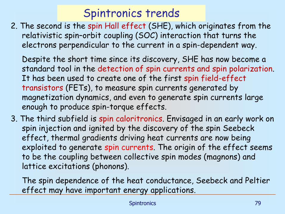
2. The second is the spin Hall effect (SHE), which originates from the relativistic spin–orbit coupling (SOC) interaction that turns the electrons perpendicular to the current in a spin-dependent way.
Despite the short time since its discovery, SHE has now become a standard tool in the detection of spin currents and spin polarization. It has been used to create one of the first spin field-effect transistors (FETs), to measure spin currents generated by magnetization dynamics, and even to generate spin currents large enough to produce spin-torque effects.
3. The third subfield is spin caloritronics. Envisaged in an early work on spin injection and ignited by the discovery of the spin Seebeckeffect, thermal gradients driving heat currents are now being exploited to generate spin currents. The origin of the effect seems to be the coupling between collective spin modes (magnons) and lattice excitations (phonons).
The spin dependence of the heat conductance, Seebeck and Peltiereffect may have important energy applications.
Spintronics trends
Spintronics

80
4. The fourth is silicon spintronics. Silicon is not only abundant (its oxide is sand) and the central material for electronics, but it also has very desirable long spin-relaxation times.
It was a late bloomer in spintronics, mostly because its indirect band gap and weak SOC have, for decades, precluded spin injection and detection.
Recent experimental breakthroughs have, however, demonstrated that the electron spin in silicon can be reliably injected and detected as well as transferred over relatively large distances, allowing a seamless integration with electronic circuits, such as connecting close-by processor cores.
5. Finally, the fifth entails the spintronic aspects of graphene and topological insulators (TIs), which originate from the band-structure properties and create an effective topological knot. This property protects the states of graphene or the surface states of a TI from non-magnetic disorder effects.
Spintronics trends
Spintronics

81
A ferromagnetic emitter to inject spin-polarized electrons via a tunnel barrier into a silicon base
These spin-polarized minority carriers traverse the base diffusively and are harvested by the ferromagnetic collectorvia another tunnel barrier
The spin selectivity derives from the back-biased collector presenting a different density of final spin states to the spin-polarized minority carriers in the base.
Silicon based spin transistor
Spintronics

Giant magnetoresistance 82
GMR through a single molecule
H2Pc (hydrogen phthalocyanine) molecules adsorbed onto two Co islands on the Cu(111) surface.
Schmaus et al., cond-mat 2011
Magnetoresistance 51%

83
Quantum devices (qubits and gates)
A SEM image of a double quantum dot
A SEM image of a two qubit device
Having nanosecond resolution one have to use a lot of high frequency components, which must all work at 40 millikelvin.
Here is a picture of a board with a sample on it. There is a microwave stripline for four coaxial cables to bring high frequency signals to the sample
Spintronics
23. In what quantum devices could spin be used? Can it be relevant to quantum computing? What are other emerging
applications of spintronics? What problems need to be solved in this area?

84
Electronics applications
Spintronics

85
• Spin injection in semiconductor – optimizing interfaces and materials are needed.
- one of ways – using magnetic semiconductors as FM decreases impedance mismatch
• Gate-induced spin rotation (Rashba effect)• Spin relaxation and decoherence
Spintronics is a new emerging field providing promising solutions for signal processing and realization of computer algorithms.
Spin depolarization is still large – many things have to be done to make coherent spintronics practical.
Current induced magnetisation switch
Problems
Spintronics