Embed Size (px)
Citation preview
Electrochimica Acta 156 (2015) 283–288
Contents lists available at ScienceDirect
Electrochimica Acta
journa l homepage: www.e lsev ier .com/ locate /e lec tac ta
Electrochemical Synthesis of PbO2, Pb3O4 and PbO Films on aTransparent Conducting Substrate
Christopher G. Poll, David J. Payne ∗
Department of Materials, Imperial College London, South Kensington, London, SW7 2AZ, United Kingdom
a r t i c l e i n f o
Article history:Received 14 November 2014Received in revised form 4 January 2015Accepted 5 January 2015Available online 7 January 2015
Keywords:PbO2
Pb3O4
PbOThin Film
a b s t r a c t
Through electroplating and thermal decomposition by annealing at various temperatures in an oxygenenvironment, films of PbO2, Pb3O4 and PbO have been synthesised on transparent conducting substratesof indium tin oxide coated glass. Of these films, Pb3O4, ˛-PbO and ˇ-PbO have a phase pure crystalstructure. These films are formed as either nano-scale particles or complete films depending on theelectroplating conditions. The complete films demonstrate excellent surface coverage with a thickness ofthe order of a few microns. The films have been characterised through a combination of x-ray diffraction,scanning electron microscopy and surface profilometry.
© 2015 Elsevier Ltd. All rights reserved.
1. Introduction
Lead oxide exists in two oxidation states, Pb4+ (PbO2) and Pb2+
(PbO), and also with multiple mixed valence states in between(Pb12O19, Pb12O17, Pb3O4) [1]. In both the 4+ and 2+ oxidation stateslead oxide takes two crystalline polymorphs, tetragonal (ˇ-PbO2,˛-PbO) and orthorhombic (˛-PbO2, ˇ-PbO) [2–5].
PbO2 has, since 1860, found wide-spread use as an electrodematerial in the lead acid battery [6], which is utilised world-widein the ignition process of the internal combustion engine in motorvehicles. PbO2 is a well studied material from an electrochemicalpoint-of-view with the various phases and surface morphologiescomprehensively reviewed [7]. Recent work, undertaken througha combination of photoemission, neutron diffraction and densityfunctional theory has identified the metallic nature of PbO2 to bedue to partial filling of conduction band states due to oxygen vacan-cies [8–11].
PbO has been demonstrated as a photoactive layer in Schottky-type photovoltaic devices [12,13] and as a surface modificationlayer in inverted polymer solar cells [14]. ˛-PbO is a material thathas potential in photovoltaic application due to its band gap of1.9 eV [15,16] whilst ˇ-PbO has suitability as a surface modificationlayer for lowering work functions [14]. The main issue associatedwith the incorporation of lead oxide in photovoltaic devices isthe fabrication of the lead oxide layer. In the work to date the
∗ Corresponding author. Tel.: +44 (0)20 759 42585.E-mail address: [email protected] (D.J. Payne).
PbO has been evaporated onto substrates, this however is not afavourable technique due to the health concerns when volatilis-ing lead. Evaporating lead and lead oxide results in contaminationof the evaporation system, and hence lead contaminants beingpresent in subsequently synthesised materials. To circumvent thisissue it is necessary to have an evaporation system solely for thepurpose of lead-based material synthesis, this approach howeveris certainly not a cost-effective one. Whilst the electrochemicalpreparation of PbO2 has been thoroughly studied [7], very littlework has been undertaken on the electrochemical synthesis of PbOfilms [17,18]. In this report we present a novel, low-cost methodfor the synthesis of PbO and Pb3O4 films on transparent conduct-ing substrates by electroplating films of PbO2 and then annealingin an air. We have produced films of various oxidation states andpolymorphs of lead oxide. Through careful control of the initialelectroplating conditions, and the annealing temperatures, we havesuccessfully synthesised films of PbO2, Pb3O4 and PbO on indiumtin oxide (ITO) coated glass, of these films Pb3O4, ˛-PbO and ˇ-PbOdemonstrate phase purity.
2. Experimental
PbO2 films have been electroplated onto ITO (8-12 �/square,Sigma-Aldrich) from a solution of 375 mM Pb(NO3)2 + 6.25 mMHNO3, which has previously been shown to be suitable for theelectrodeposition of PbO2 [8,9,19,20], maintained at 60 ◦C using awater bath. The Pb(NO3)2 (≥99.0% purity) and HNO3 were usedas supplied from Sigma-Aldrich and diluted with ultra-pure Milli-Q water. The ITO electrode, assigned as the anode, was prepared
http://dx.doi.org/10.1016/j.electacta.2015.01.0190013-4686/© 2015 Elsevier Ltd. All rights reserved.
284 C.G. Poll, D.J. Payne / Electrochimica Acta 156 (2015) 283–288
through ultrasonic cleaning in acetone, isopropanol and ultra-pureMilli-Q water and dried with N2 gas, a Pt electrode was used asthe cathode. A current density of 10 mAcm−2 was applied for var-ious plating times using a Keithley 2200-30-5 DC power supply.This current density was chosen as it provided films with optimalsurface coverage. Following the electroplating the PbO2 films wererinsed of any residual solution using Milli-Q water and dried withN2 gas. The films were then thermally decomposed using a tubefurnace at various temperatures in air for 6 hours.
The crystal structure and oxidation state of the films was stud-ied using x-ray diffraction (XRD) with a Panalytical X’Pert ProX-Ray Diffractometer. The assignment of diffraction peaks has beenundertaken using the Inorganic Crystal Structure Database (ICSD)(icsd.cds.rsc.org). Scanning electron microscopy (SEM) images havebeen recorded with a JEOL JSM5610LV electron microscope andhigh-resolution scanning electron microscopy (HR-SEM) imageswith a LEO Gemini 1525 electron microscope. Film thicknesses havebeen measured using a Dektak profilometer.
3. Results and Analysis
PbO2 films were electroplated for incremental time periods of 1second, 2 seconds, 5 seconds and 5 minutes. The films were visu-ally smooth and demonstrated excellent surface coverage. The filmcolour ranged from a translucent very light brown colour follow-ing 1 second of growth through to a dark brown colour followingextended growth time. Films grown for 5 minutes were a dark grey/ black colour and opaque in appearance. The XRD patterns of thesefilms are presented in Fig. 1.
It can be seen that following 1 second of growth only mini-mal PbO2 is present, which appears in the ˇ-phase, however asthe growth time continues through 2 and 5 seconds these ˇ-PbO2peaks become more intense. The observed In2O3 peaks are presentdue to the ITO substrate. Following 5 seconds of growth, as well asthere being ˇ-PbO2 present, there is additionally ˛-PbO2 beginningto appear. After 5 minutes of growth the film has a mixed phase ofboth ˛- and ˇ-PbO2, with the ˇ-PbO2 dominating the diffractionpattern, at this point there are additionally no diffraction peaksfrom the In2O3, suggesting a thick and complete surface coverage.
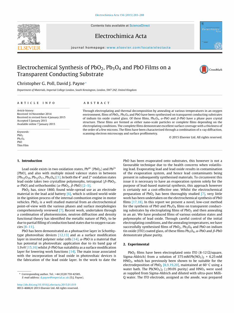
The film thicknesses, measured by profilometry, were deter-mined to be 99 ± 10 nm, 134 ± 6 nm, 200 ± 14 nm and 3.2 ± 0.2 �mfor the films grown for 1 second, 2 seconds, 5 seconds and 5 minutesrespectively. The thicknesses were measured at multiple points oneach film with the average then calculated. The uncertainty repre-sents the standard error in the mean. SEM and HR-SEM images ofthe films are presented in Fig. 2, it can be seen that for the shorterplating times (1, 2, 5 seconds) the films are structured as a series ofPbO2 particles on the ITO substrate, however following the longer5 minute electroplating a complete film of micro-scale crystalliteshas formed.
The particles appearing in the HR-SEM images can be attributedto PbO2, as when recording a control image of bare ITO these werenot present. The PbO2 particles can be seen to grow with increasedelectroplating time. This result suggests that it is more energeti-cally favourable for the PbO2 to deposit on PbO2 nucleation sitesrather than directly onto the ITO. The presence of In2O3 in the XRDpatterns in Fig. 1 for the films electroplated for 1 second, 2 secondsand 5 seconds is clearly due to incomplete surface coverage andlarge areas of ITO still being exposed. By 5 minutes however thereis complete coverage and the films are considerably thicker. TheXRD patterns of the PbO2 distinctly demonstrate polycrystallinefilms, the SEM images reflect this with the large volume of crystalgrains observed with lots of variation in their orientations.
It is well known that ˇ-PbO2 reduces to ˛-PbO at 572 ◦C for pow-dered samples [9,22,23]. It is also reported that PbO2 can be reduced
10 15 20 25 30 35 40 45 50 55 60 65 70
(a)1 second
(b)2 seconds
(c)5 seconds
(d)5 minutes
β-PbO2
α-PbO2
In2O3
2θ (°)
Fig. 1. XRD patterns of PbO2 films electroplated from 375 mM Pb(NO3)2 +6.25 mM HNO3 with a current density of 10 mAcm−2 on ITO for (a) 1 second, (b)2 seconds, (c) 5 seconds and (d) 5 minutes. The XRD peak assignment has beenundertaken using the ICSD with reference patterns of ˛-PbO2 [2], ˇ-PbO2 [3] andIn2O3 [21].
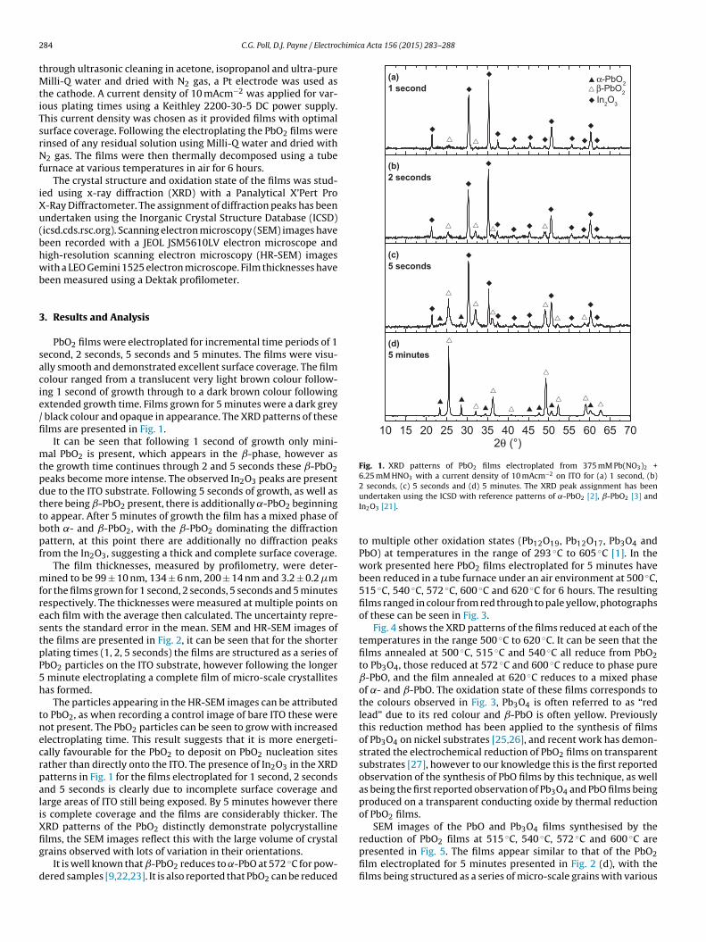
to multiple other oxidation states (Pb12O19, Pb12O17, Pb3O4 andPbO) at temperatures in the range of 293 ◦C to 605 ◦C [1]. In thework presented here PbO2 films electroplated for 5 minutes havebeen reduced in a tube furnace under an air environment at 500 ◦C,515 ◦C, 540 ◦C, 572 ◦C, 600 ◦C and 620 ◦C for 6 hours. The resultingfilms ranged in colour from red through to pale yellow, photographsof these can be seen in Fig. 3.
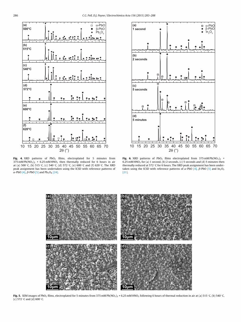
Fig. 4 shows the XRD patterns of the films reduced at each of thetemperatures in the range 500 ◦C to 620 ◦C. It can be seen that thefilms annealed at 500 ◦C, 515 ◦C and 540 ◦C all reduce from PbO2to Pb3O4, those reduced at 572 ◦C and 600 ◦C reduce to phase pureˇ-PbO, and the film annealed at 620 ◦C reduces to a mixed phaseof ˛- and ˇ-PbO. The oxidation state of these films corresponds tothe colours observed in Fig. 3, Pb3O4 is often referred to as “redlead” due to its red colour and ˇ-PbO is often yellow. Previouslythis reduction method has been applied to the synthesis of filmsof Pb3O4 on nickel substrates [25,26], and recent work has demon-strated the electrochemical reduction of PbO2 films on transparentsubstrates [27], however to our knowledge this is the first reportedobservation of the synthesis of PbO films by this technique, as wellas being the first reported observation of Pb3O4 and PbO films beingproduced on a transparent conducting oxide by thermal reductionof PbO2 films.
SEM images of the PbO and Pb3O4 films synthesised by thereduction of PbO2 films at 515 ◦C, 540 ◦C, 572 ◦C and 600 ◦C arepresented in Fig. 5. The films appear similar to that of the PbO2film electroplated for 5 minutes presented in Fig. 2 (d), with thefilms being structured as a series of micro-scale grains with various
C.G. Poll, D.J. Payne / Electrochimica Acta 156 (2015) 283–288 285
Fig. 2. SEM images of PbO2 electroplated on ITO from 375 mM Pb(NO3)2 + 6.25 mM HNO3 at 10 mAcm−2 for (a) 1 second (b) 2 seconds, (c) 5 seconds recorded with HR-SEM,and with standard SEM for (d) 5 minutes of electroplating.
orientations. Much like for the PbO2 film, this explains the multiplediffraction peaks for each material. On closer inspection it can beseen that the grains in the Pb3O4 and PbO films are not as sharplydefined as those in the PbO2 films, the edges of the grains appearsmoother. This is likely due to the elevated temperature relaxingthe shape of the grains. The grains of the film annealed at 600 ◦Cappear to be smoothed more than those of the film annealed at515 ◦C, suggesting that as the temperature increases further so doesthe relaxation of the grain structure. On the micro-scale, as wellas the macro-scale (demonstrated by the photographs and SEMimages respectively) the films can be observed to have excellentcoverage with minimal fracturing and degradation.
Films of PbO2 electroplated from 375 mM Pb(NO3)2 +6.25 mM HNO3 for 1 second, 2 seconds, 5 seconds and 5 min-utes have been thermally reduced at 572 ◦C for 6 hours to studythe effect of electroplating time on the reduced films. XRD patternsof these films are presented in Fig. 6. Annealing a PbO2 film at572 ◦C which has been electroplated for 5 minutes leads to aphase pure ˇ-PbO film, however PbO2 films which have beenelectroplated for 2 seconds and 5 seconds form ˛-PbO when
annealed at this temperature. The PbO2 film that had been elec-troplated for 1 second showed no evidence of any phase of PbOfollowing reduction at 572 ◦C, the only peaks visible were thoseof In2O3 from the ITO substrate, suggesting the lead oxide hasbeen lost during the annealing process. The difference in phase of˛-PbO and ˇ-PbO between the reduced films electroplated for 2seconds and 5 seconds, and those electroplated for 5 minutes canbe understood when considering the XRD patterns of the PbO2films electroplated for these times, pre-annealing, in Fig. 1 (b),(c) and (d). It can be seen that the PbO2 films electroplated for 2seconds and 5 seconds are predominantly of the tetragonal ˇ-PbO2phase, with only a negligible orthorhombic ˛-PbO2 contributionin the film electroplated for 5 seconds. However, the PbO2 filmelectroplated for 5 minutes contains significant quantities of both˛- and ˇ-PbO2. The difference in phase of the reduced films withrespect to the deposition time could be explained by it beingan energetically favourable process for the tetragonal ˇ-PbO2 toreduce to the tetragonal ˛-PbO, whereas in the film electroplatedfor 5 minutes the significant orthorhombic ˛-PbO2 could be actingas “seeding” sites for the formation of orthorhombic ˇ-PbO. The
Fig. 3. Photographs of PbO2 films (electroplated for 5 minutes) reduced for 6 hours in air at (a) 500 ◦C, (b) 515 ◦C, (c) 540 ◦C, (d) 572 ◦C, (e) 600 ◦C and (f) 620 ◦C.
286 C.G. Poll, D.J. Payne / Electrochimica Acta 156 (2015) 283–288
10 15 20 25 30 35 40 45 50 55 60 65 70
(a)500°C
α-PbOβ-PbOPb3O4
(b)515°C
(c)540°C
(d)572°C
(e)600°C
(f)620°C
2θ (°)
Fig. 4. XRD patterns of PbO2 films, electroplated for 5 minutes from375 mM Pb(NO3)2 + 6.25 mM HNO3 then thermally reduced for 6 hours in airat (a) 500 ◦C, (b) 515 ◦C, (c) 540 ◦C, (d) 572 ◦C, (e) 600 ◦C and (f) 620 ◦C. The XRDpeak assignment has been undertaken using the ICSD with reference patterns of˛-PbO [4], ˇ-PbO [5] and Pb3O4 [24].
10 15 20 25 30 35 40 45 50 55 60 65 70
(a)1 second
α-PbOβ-PbOIn2O3
(b)2 seconds
(c)5 seconds
(d)5 minutes
2θ (°)
Fig. 6. XRD patterns of PbO2 films electroplated from 375 mM Pb(NO3)2 +6.25 mM HNO3 for (a) 1 second, (b) 2 seconds, (c) 5 seconds and (d) 5 minutes thenthermally reduced at 572 ◦C for 6 hours. The XRD peak assignment has been under-taken using the ICSD with reference patterns of ˛-PbO [4], ˇ-PbO [5] and In2O3
[21].
Fig. 5. SEM images of PbO2 films, electroplated for 5 minutes from 375 mM Pb(NO3)2 + 6.25 mM HNO3 following 6 hours of thermal reduction in air at (a) 515 ◦C, (b) 540 ◦C,(c) 572 ◦C and (d) 600 ◦C.
C.G. Poll, D.J. Payne / Electrochimica Acta 156 (2015) 283–288 287
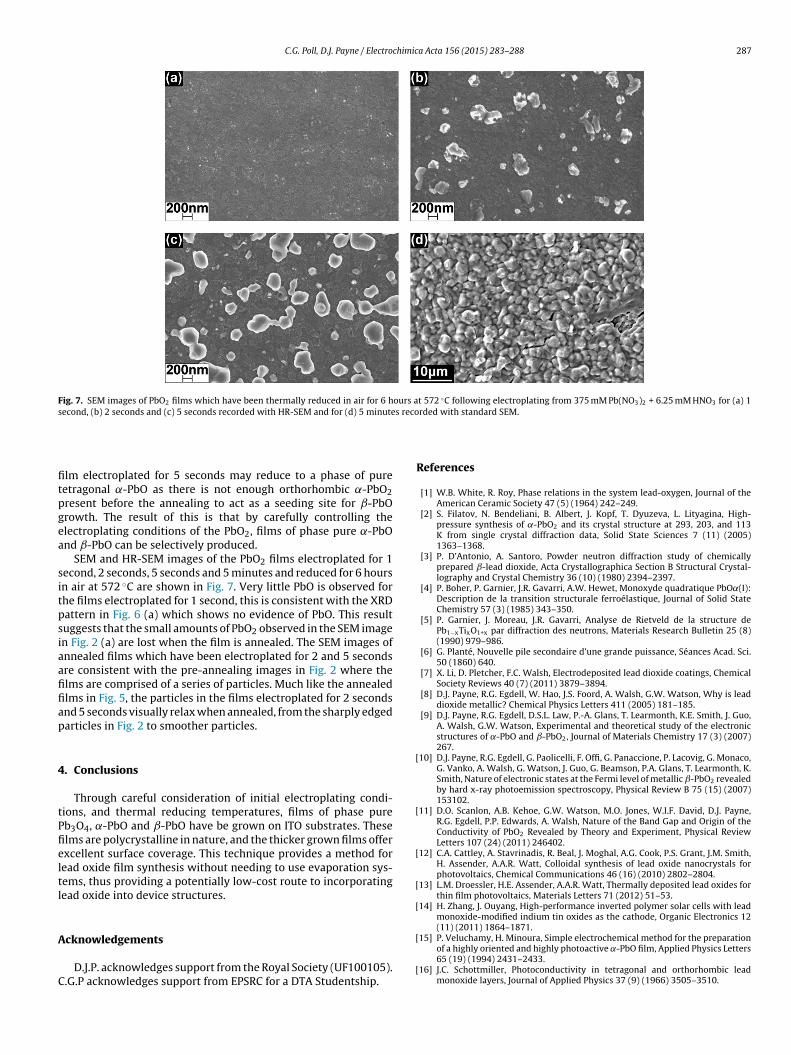
Fig. 7. SEM images of PbO2 films which have been thermally reduced in air for 6 hours at 572 ◦C following electroplating from 375 mM Pb(NO3)2 + 6.25 mM HNO3 for (a) 1second, (b) 2 seconds and (c) 5 seconds recorded with HR-SEM and for (d) 5 minutes recorded with standard SEM.
film electroplated for 5 seconds may reduce to a phase of puretetragonal ˛-PbO as there is not enough orthorhombic ˛-PbO2present before the annealing to act as a seeding site for ˇ-PbOgrowth. The result of this is that by carefully controlling theelectroplating conditions of the PbO2, films of phase pure ˛-PbOand ˇ-PbO can be selectively produced.
SEM and HR-SEM images of the PbO2 films electroplated for 1second, 2 seconds, 5 seconds and 5 minutes and reduced for 6 hoursin air at 572 ◦C are shown in Fig. 7. Very little PbO is observed forthe films electroplated for 1 second, this is consistent with the XRDpattern in Fig. 6 (a) which shows no evidence of PbO. This resultsuggests that the small amounts of PbO2 observed in the SEM imagein Fig. 2 (a) are lost when the film is annealed. The SEM images ofannealed films which have been electroplated for 2 and 5 secondsare consistent with the pre-annealing images in Fig. 2 where thefilms are comprised of a series of particles. Much like the annealedfilms in Fig. 5, the particles in the films electroplated for 2 secondsand 5 seconds visually relax when annealed, from the sharply edgedparticles in Fig. 2 to smoother particles.
4. Conclusions
Through careful consideration of initial electroplating condi-tions, and thermal reducing temperatures, films of phase purePb3O4, ˛-PbO and ˇ-PbO have be grown on ITO substrates. Thesefilms are polycrystalline in nature, and the thicker grown films offerexcellent surface coverage. This technique provides a method forlead oxide film synthesis without needing to use evaporation sys-tems, thus providing a potentially low-cost route to incorporatinglead oxide into device structures.
Acknowledgements
D.J.P. acknowledges support from the Royal Society (UF100105).C.G.P acknowledges support from EPSRC for a DTA Studentship.
References
[1] W.B. White, R. Roy, Phase relations in the system lead-oxygen, Journal of theAmerican Ceramic Society 47 (5) (1964) 242–249.
[2] S. Filatov, N. Bendeliani, B. Albert, J. Kopf, T. Dyuzeva, L. Lityagina, High-pressure synthesis of ˛-PbO2 and its crystal structure at 293, 203, and 113K from single crystal diffraction data, Solid State Sciences 7 (11) (2005)1363–1368.
[3] P. D’Antonio, A. Santoro, Powder neutron diffraction study of chemicallyprepared ˇ-lead dioxide, Acta Crystallographica Section B Structural Crystal-lography and Crystal Chemistry 36 (10) (1980) 2394–2397.
[4] P. Boher, P. Garnier, J.R. Gavarri, A.W. Hewet, Monoxyde quadratique PbO˛(I):Description de la transition structurale ferroélastique, Journal of Solid StateChemistry 57 (3) (1985) 343–350.
[5] P. Garnier, J. Moreau, J.R. Gavarri, Analyse de Rietveld de la structure dePb1−xTixO1+x par diffraction des neutrons, Materials Research Bulletin 25 (8)(1990) 979–986.
[6] G. Planté, Nouvelle pile secondaire d’une grande puissance, Séances Acad. Sci.50 (1860) 640.
[7] X. Li, D. Pletcher, F.C. Walsh, Electrodeposited lead dioxide coatings, ChemicalSociety Reviews 40 (7) (2011) 3879–3894.
[8] D.J. Payne, R.G. Egdell, W. Hao, J.S. Foord, A. Walsh, G.W. Watson, Why is leaddioxide metallic? Chemical Physics Letters 411 (2005) 181–185.
[9] D.J. Payne, R.G. Egdell, D.S.L. Law, P.-A. Glans, T. Learmonth, K.E. Smith, J. Guo,A. Walsh, G.W. Watson, Experimental and theoretical study of the electronicstructures of ˛-PbO and ˇ-PbO2, Journal of Materials Chemistry 17 (3) (2007)267.
[10] D.J. Payne, R.G. Egdell, G. Paolicelli, F. Offi, G. Panaccione, P. Lacovig, G. Monaco,G. Vanko, A. Walsh, G. Watson, J. Guo, G. Beamson, P.A. Glans, T. Learmonth, K.Smith, Nature of electronic states at the Fermi level of metallic ˇ-PbO2 revealedby hard x-ray photoemission spectroscopy, Physical Review B 75 (15) (2007)153102.
[11] D.O. Scanlon, A.B. Kehoe, G.W. Watson, M.O. Jones, W.I.F. David, D.J. Payne,R.G. Egdell, P.P. Edwards, A. Walsh, Nature of the Band Gap and Origin of theConductivity of PbO2 Revealed by Theory and Experiment, Physical ReviewLetters 107 (24) (2011) 246402.
[12] C.A. Cattley, A. Stavrinadis, R. Beal, J. Moghal, A.G. Cook, P.S. Grant, J.M. Smith,H. Assender, A.A.R. Watt, Colloidal synthesis of lead oxide nanocrystals forphotovoltaics, Chemical Communications 46 (16) (2010) 2802–2804.
[13] L.M. Droessler, H.E. Assender, A.A.R. Watt, Thermally deposited lead oxides forthin film photovoltaics, Materials Letters 71 (2012) 51–53.
[14] H. Zhang, J. Ouyang, High-performance inverted polymer solar cells with leadmonoxide-modified indium tin oxides as the cathode, Organic Electronics 12(11) (2011) 1864–1871.
[15] P. Veluchamy, H. Minoura, Simple electrochemical method for the preparationof a highly oriented and highly photoactive ˛-PbO film, Applied Physics Letters65 (19) (1994) 2431–2433.
[16] J.C. Schottmiller, Photoconductivity in tetragonal and orthorhombic leadmonoxide layers, Journal of Applied Physics 37 (9) (1966) 3505–3510.

288 C.G. Poll, D.J. Payne / Electrochimica Acta 156 (2015) 283–288
[17] S. Sawatani, S. Ogawa, T. Yoshida, H. Minoura, Formation of highly crystallizedˇ-PbO thin films by cathodic electrodeposition of Pb and its rapid oxidation inair, Advanced Functional Materials 15 (2) (2005) 297–301.
[18] I. Zhitomirsky, L. Gal-Or, A. Kohn, H.W. Hennicke, Electrochemical preparationof PbO films, Journal of Materials Science Letters 14 (11) (1995) 807–810.
[19] D.J. Payne, G. Paolicelli, F. Offi, G. Panaccione, P. Lacovig, G. Beamson, A. Fon-dacaro, G. Monaco, G. Vanko, R.G. Egdell, A study of core and valence levelsin ˇ-PbO2 by hard x-ray photoemission, Journal of Electron Spectroscopy andRelated Phenomena 169 (1) (2009) 26–34.
[20] A.B. Velichenko, R. Amadelli, A. Benedetti, D.V. Girenko, S.V. Kovalyov, F.I.Danilov, Electrosynthesis and physicochemical properties of PbO2 Films, Jour-nal of The Electrochemical Society 149 (9) (2002) C445–C449.
[21] M. Marezio, Refinement of the crystal structure of In2O3 at two wavelengths,Acta Crystallographica 20 (6) (1966) 723–728.
[22] D.J. Payne, R.G. Egdell, A. Walsh, G.W. Watson, J. Guo, P.-A. Glans, T. Learmonth,K.E. Smith, Electronic origins of structural distortions in post-transition metal
oxides: experimental and theoretical evidence for a revision of the lone pairmodel, Physical Review Letters 96 (15) (2006) 1–4.
[23] D. Le Bellac, J. Kiat, P. Garnier, H. Moudden, P. Sciau, P. Buffat, G. André, Mecha-nism of the incommensurate phase in lead oxide ˛-PbO, Physical Review B 52(18) (1995) 13184–13194.
[24] J.-R. Gavarri, D. Weigel, Oxydes de plomb. I. Structure cristalline du miniumPb3O4, à température ambiante (293 K), Journal of Solid State Chemistry 13 (3)(1975) 252–257.
[25] M. Sharon, S. Kumar, S.R. Jawalekar, Characterization of Pb3O4 films by electro-chemical techniques, Bulletin of Materials Science 8 (3) (1986) 415–418.
[26] S. Kumar, M. Sharon, S.R. Jawalekar, Preparation of a thin film of Pb3O4
by thermal treatment of PbO2 film, Thin Solid Films 195 (1-2) (1991)273–278.
[27] D.V. Girenko, A.B. Velichenko, E. Mahé, D. Devilliers, Electrodeposition of thinelectrocatalytic PbO2 layer on fluorine-doped tin oxide substrates, Journal ofElectroanalytical Chemistry 712 (2014) 194–201.