Embed Size (px)
Citation preview
Journal of The Electrochemical Society, 151 ~3! A470-A483 ~2004!0013-4651/2004/151~3!/A470/14/$7.00 © The Electrochemical Society, Inc.
A470
Electrochemical and In Situ XRD Studies of the Li Reactionwith Combinatorially Sputtered Mo 1ÀxSnx „0 Ï x Ï 0.50…Thin FilmsA. Bonakdarpour,a K. C. Hewitt, a R. L. Turner, b,* and J. R. Dahna,* ,z
aDepartment of Physics, Dalhousie University, Halifax, Nova Scotia, B3H 3J5, Canadab3M Company, 3M Center, St. Paul, Minnesota, 55144, USA
Detailed electrochemical studies of the reaction of Li with combinatorially sputter-deposited BCC (x < 0.4) and nanocrystalline(x > 0.4) Mo12xSnx thin films are reported for 0.05< x < 0.5. In situ X-ray diffraction ~XRD! performed forx 5 0.22, 0.36,0.44, show no evidence for formation of new phases during the reaction with Li. During charge/discharge cycling, a definite andperiodic variation of the BCC Mo12xSnx ~110! Bragg angle forx < 0.40 is strong evidence for a topotactic Li insertion mecha-nism. Sensitive differential capacity (dq/dV vs. V) measurements on Li/Mo12xSnx cells withx < 0.36 show no new peaks for asmany 75 cycles, supporting a topotactic insertion reaction. However, in the higher Sn content films (x > 0.4), the appearance andgrowth of newdq/dV peaks after the first cycle is consistent with the aggregation of Sn clusters and the formation of Li-Snphases. Inclusion of about 20% oxygen in nanostructured films seems to prevent Sn aggregation and improve the cyclingperformance markedly. The best materials give specific capacities near 350 mAh/g, have densities near 9 g/cc and cycle well. Thiscould be the first report of true topotactic Li insertion into a metal host.© 2004 The Electrochemical Society.@DOI: 10.1149/1.1646138# All rights reserved.
Manuscript submitted November 14, 2002; revised manuscript received August 20, 2003. Available electronically February 11,2004.
rialsanodve elnd
onlyllineintingvol-
elec-erm
hice asof
ix ofe th
acityl,Lithoured
nndg-sho
ionst thele.bynl
d cy-
fion
on of-Thei re-
s-
allyand
nd the
-d in
-,
/gudys
een-n thew-sP. G.tech--ctro-
lystss oftalytici-ionring-
sitiono totteredin then of
st toterizeearchom-
e-cal
The need for higher energy Li-ion battery electrode matewith higher energy has driven research on both cathode andmaterials. For anode materials, research has centered on actiments like Sn or Si, which alloy with Li and have gravimetric avolumetric capacities up to ten times that of graphite commused in today’s commercial Li-ion batteries. However, crystabinary Li alloys LixM (M 5 Si,Sn,Al), suffer from severe grafragmentation during lithiation/delithiation because coexisphases with different Li concentrations lead to inhomogeneousume expansions. Cracking of the alloy grains results in loss oftrical contact or poor conductivity and this hinders the long tcycling performance.1
For instance, LixSn goes through five different crystallograpphases for (0, x , 4.2) and the volume changes are as larg300%. As a remedy, Besenhardet al. suggested the incorporationnanosized active alloying species like Sn in an inactive matrSnSb, in order to suppress Li-Sn phase transitions and improvcycling behavior.2 Nanosized active Sn2Fe mixed with inactiveSnFe3C has also shown improved performance.3
One very appealing idea would be to synthesize a high caplow-voltage, Sn-based~or other active element! insertion materiawhich is truly topotactici.e., the host retains its structure duringinsertion/removal and hundreds of cycles can be obtained wiany significant loss of capacity. The Li insertion reaction in layestructures like LixCoO2 and LixC6 is topotactic. The reaction of Li iternary systems like LiMM8, where M is an alloying element aM8 is an inactive element like Cu6Sn5 and InSb, have been sugested to be insertion/displacement reactions that subsequentlyreactions with small volume expansions upon reaction with Li.4,5 Infact, both Cu6Sn5 and InSb were first reported to show some regof topotactic Li insertion; however further research showed thareaction of Li with these intermetallic compounds is more subt
For Cu6Sn5 , carefulin situ X-ray and Mossbauer experimentsLarcheret al.6 and Franssonet al.7 showed that upon full lithiatioCu is extruded from Li2Cu6Sn5 yielding Li4.4Sn and Cu as finaproducts. The charge reaction is not completely reversible ancling performance improves somewhat only when Li/Cu6Sn5 cellsare discharged only to 0.2 V~or to a limiting composition oLi2Cu6Sn5), preventing Cu extrusion. For InSb, the full react
* Electrochemical Society Active Member.z E-mail: [email protected]
ee-
e
,
t
w
with Li causes the destruction of the compound and the formatiLi 3Sb, LiIn, and Li3In2 phases.8 Neither Cu6Sn5 or InSb is a topotactic Li insertion compound over the entire voltage range.Mo12xSnx phases reported here, however, may indeed insert Lversibly during charge/discharge forx , 0.36, even when dicharged to 0 V.
In an earlier paper9 we reported the properties of sequentisputtered Mo-Sn films, where a variety of crystal structuresnanostructures were obtained depending on the composition asputtering conditions. We prepared crystalline BCC Mo12xSnx (x, 0.42), nanocrystalline BCC Mo12xSnx coexisting with nanocrystalline Sn (x . 0.45), and nanoscopic regions of Sn embeddelamina of composition modulated Mo12xSnx (x . 0.4).9 The electrochemical behavior of the films forx , 0.5 were very promisingfor example nanostructured Mo0.5Sn0.5 delivered about 250 mAhfor about 200 cycles.10 We therefore decided to prepare and stthe composition range 0, x , 0.5 in Mo12xSnx using the methodof combinatorial materials science~CMS!.
Combinatorial chemistry, or parallel fabrication and rapid scring of new materials, has been a well-established method idiscovery of new pharmaceutical drugs.11 In the past decade, hoever, based on the pioneering work of J. J. Hanak12 and coworkerin the 1970s, Berkeley researchers including X. D. Xiang andSchultz13 developed and applied sophisticated combinatorialniques to synthesize and study solid materials like HTc superconductors, dielectrics, and fuel cell catalysts. Combinatorial elechemistry was perhaps first introduced by Reddingtonet al. whodescribed a method of producing libraries of metal alloy catafor methanol oxidation, whereby a few hundred combinationmetals were printed on Toray paper and screened for their caactivity.14 In the search for anode and cathode materials for Lbatteries, we recently developed a simple but powerful sputtebased methodology, which can continuously map the compospaces of materials in 1 and 2 dimensional thin film libraries. Twfour targets, which can be elements or compounds, are spusimultaneously and the sputtered beams are masked to obtadesired composition variation in the films. A detailed descriptioour approach is reported elsewhere.15
The broad objective of this study has been really twofold: Firestablish a CMS technique to synthesize and characcomposition-graded films and second to use these films in the sfor new anode materials for Li-ion batteries. The deposition, cposition and structure of the Mo12xSnx films studied here are rported in a related paper.16 Here, we will present the electrochemi
ic Lihe
ande ofhencticeLi to
rom
thine--leetronoutSn
icalac-
g run.nedt Molefront
n andue ofutmix-
n is aadius
wer,
7
se
Journal of The Electrochemical Society, 151 ~3! A470-A483 ~2004! A471
properties of these films and provide evidence for a topotactinsertion mechanism in Mo12xSnx (x , 0.36). We also discuss trole of long range ordering~i.e., crystallinevs.nanocrystalline! andoxygen in the host on the voltage profile, specific capacity,cycling performance. In this paper, we refer to the dischargLi/Mo12xSnx cells as the direction of current flow that occurs wthe cells are connected to a resistive load, as is common praThis means that discharge of the cells corresponds to addingMo12xSnx and charge of the cells corresponds to removing Li fMo12xSnx .
Experimental
A detailed description of our combinatorial approach andfilm deposition procedures for Mo12xSnx are reported in a complmentary paper, but will be briefly recapitulated here.15 The composition range 0, x , xmax in Mo12xSnx was produced in a singsputter deposition by a Corona Vacuum Coaters V3T magnsputtering system which reaches a base pressure of ab3 1028 Torr. Two-inch diameter targets of 99.9% pure Mo and
Table I. Summary of Mo-Sn sputtering experiments used for electr
GrowthID
Ar Flowrate
~sccm!
Argonpressure~mTorr!
~P~W
Run129a 15 2 125SPD74 2.5 3.2 50SPD99 8.5 10 25SPD103 1.0 1.8 25SPE5 0.6 1.5 28SPE21 0.6 1.4 28SPF6c 0.90 1.0 25SPF66 1.0 1.0 3SPG30 3.5Ar/0.5O2 3.5 49/
a Run129 was deposited at a larger target-substrate distance thus ab P 5 power, V5 voltage, and I5 current.c For SPF6 no masks were used, the growth was aimed at a fixed c
Table II. Summary of the structure and composition of the Mo-Sn
ID x in Mo12xSnx y in @MoSn#12yOy
T
SPD74 0.04-0.47 0.44 to 0.22 0.6
SPD99 0.02-0.36 ;0.4 0.0SPD103 0.05-0.92 ;0.1
SPE5 0.02-0.50 None for 0.3, x , 0.5;0.10 forx , 0.3
0.7
SPE21 0.03-0.5 None forx . 0.25;0.06 forx . 0.25
0.7
SPF6 0.30 ;0.05SPF66 0.05-0.5 0 for x , 0.2
0.05 forx . 0.2
SPG30 0.02-0.44 0.2 , y0.5for 0.02, x , 0.5
0.
.
7
~Kurt J. Lesker! were sputtered by dc power supplies~AdvancedEnergy MDX-1K! onto 1.3 cm diam Cu disks for electrochemcells, onto 3.03 1.0 in. glass microscope slides for X-ray diffrtion ~XRD! and microprobe analysis, and onto Be disks forin situXRD studies. All substrates were coated in the same sputterin
To map out the stoichiometry of the film, a mask was desigand placed in front of the Mo target. This mask causes constandeposition~mass per unit area! vs. position on the substrate tabthat rotates during the deposition. A different shaped mask inof Sn target causes a linearly varying Sn depositionvs.radius on thesubstrate. By first measuring the deposition rates of Mo and Sthen adjusting the sputtering powers one can control the valxmax in Mo12xSnx (0 , x , xmax).
15 The table was rotated at abo30 rpm during the sputtering runs and this lead to an intimateture of the sputtered Mo and Sn atoms. The sputtered regiodonut-shaped ring with an inner radius of 9.5 cm and an outer rof 17 cm. At the inner radius, the composition isx 5 xmax inMo12xSnx and at the outer radius the composition isx 5 0 inMo12xSnx . The sputtering parameters, including pressure, po
mical studies.
b
!
Mo~P/V/I!
~W/V/A !
Sputteringtime
~hours!
Rotationspeed~rpm!
0.33 300/332/0.90 10 25/0.15 149/362/0.41 6 30/0.09 75/255/0.30 5.8 23/0.23 75/323/0.23 6.0 23/0.08 75/315/0.231 9.0 170.085 75/295/0.247 9.0 10.06 117/494/0.233 1.5 17/0.1 100/337/0.29 2.5 17.163 150/290/0.515 2.5 30
r time.
sition ofx 5 0.30.
red films.
esst! Structure and phases
, 1.2 Nanosized BCC forx . 0.12Single phase rock salt forx , 0.12, possibly a Mo-O pha
, 0.85 Broad BCC peaks ‘‘powder-like’’ patternCrystalline Sn forx ; 0.91
Nanosized BCC (Mo0.63Sn0.37) and Sn for 0.37, x , 0.9Nanosized and crystalline BCC forx . 0.34
BCC and Mo3Sn-type for0.1 , x , 0.33
BCC phase belowx 5 0.1, 1.64 Nanosized BCC forx . 0.36,
Crystalline BCC forx , 0.36BCC and Mo3Sn mixture for 0.11, x , 0.31
, 1.9 Nanosized BCC for X. 0.40,
Crystalline BCC for X, 0.40BCC and Mo3Sn for 0.10, x , 0.33
BCC for x , 0.101 BCC phase
BCC for 0.05, x , 0.38
Nanocrystalline forx . 0.38, 1.3 Nanocrystalline
oche
Sn/V/I!/V/A
/376//346/274/378/339/313//358/5/339283/0
longe
ompo
sputte
hickn~mm
5, t
4, t
, t
5, t
;
5 , t
ed in
XA-
an-lyze
de-tectoKd x-yina-
en is
ithsed.
5°thirdnereum-each
s be-lancessximate
ofofmg
sing
d by
lesar
Journal of The Electrochemical Society, 151 ~3! A470-A483 ~2004!A472
voltage, and current for the different sample films are summarizTable I.
Composition analysis of the films was made using a JEOL J8200 Superprobe equipped with one energy dispersive~EDS! spec-trometer, five wavelength dispersive~WDS! spectrometers, andautomated motion stage. The metal content~Mo, Sn, and Cu/Si substrate!, was measured by EDS and the oxygen content was anaby WDS.
For rapid structural analysis of the entire composition rangeposited on a glass slide, an Inel curved position sensitive de~CPS 120! and a PW-1720 Phillips X-ray generator using Cuaradiation was used. The system is equipped with an automatemotion stage, which makes it an ideal tool for analyzing comb
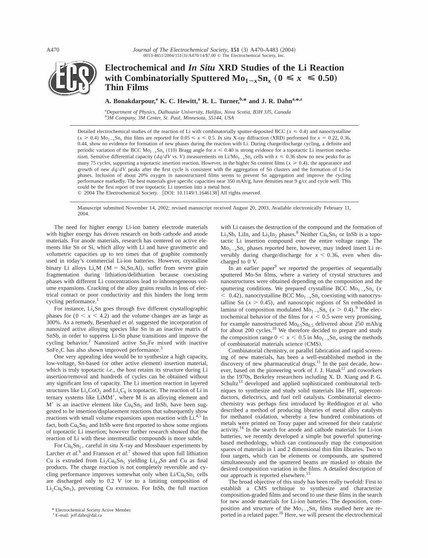
Figure 1. x in Mo12xSnx , as measured by electron microprobe,vs.positionfor a film ~SPD103! sputter deposited on a glass microscope slide ucombinatorial methods.
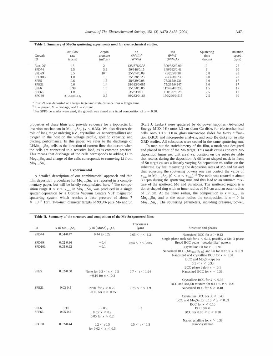
Figure 2. XRD patterns taken at different positions on the slide describeFig. 1. The structure changes from crystalline tetragonal Sn~near x5 0.91) to BCC Mo0.9Sn0.1. Open circles, solid squares, and solid circdenote Mo3Sn-type, BCC Mo12xSnx , and crystalline Sn, respectively. Ne2u 5 40°, peaks of the BCC Mo12xSnx phase and the Mo3Sn phaseoverlap.16 The uncertainty in the values ofx is about60.02.
d
r
torial samples. The size of the X-ray beam spot on the specimabout 1 by 1 mm.
For in situ XRD, a Siemens D5000 diffractometer equipped wCu Ka radiation and a diffracted beam monochromator was uEach in situ X-ray scan took about 3 h and was collected in 0.0increments between scattering angles of 20 and 50°. Everyscan was made between 20°, 2u , 80°. For the experiment onanostructured Mo12xSnx with x 5 0.44, three adjacent scans wbinned together to improve the signal to noise ratio. Table II smarizes the crystal structure and composition of regions infilm.
The deposited mass was obtained by weighing the Cu diskfore and after the deposition using a precision Cahn 29 microbawith a 1 3 1027 g resolution. An approximation of film thicknewas made using the deposited mass and assuming an approdensity r 5 (1 2 x) rMo 1 xrSn with the nominal densitiesrMo 5 10.2 andrSn 5 7.3 g/cm3. The active mass and thicknessthe 1.3 cm diam electrodes varied from approximately 0.5 to 2and from 0.5 to 1mm from x 5 0.05 to x 5 0.5 in Mo12xSnx ,respectively.
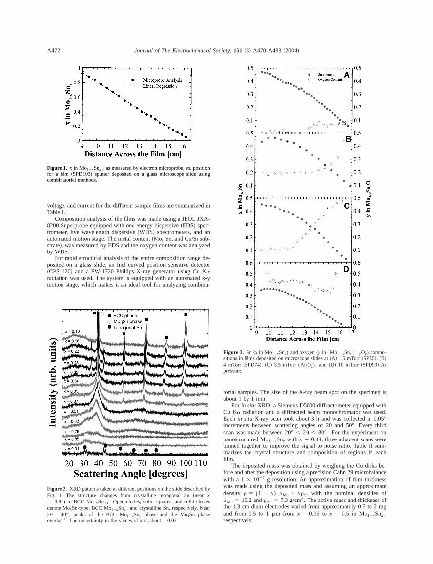
Figure 3. Sn ~x in Mo12xSnx) and oxygen~y in @Mo12xSnx#12yOy) compo-sitions in films deposited on microscope slides at~A! 1.5 mTorr~SPE5!, ~B!4 mTorr ~SPD74!, ~C! 3.5 mTorr (Ar/O2), and ~D! 10 mTorr ~SPD99! Arpressure.
itionpo-trodeaperd in
es toever,ts that
sition
as
lledmem-di-s
0 anded at
f 4.4is
-d Sn.
no.2325h there 22,40,
for.
using
cellswereircuitsial wasare
0.
ge
e
ed
ed
rge
ec-
Journal of The Electrochemical Society, 151 ~3! A470-A483 ~2004! A473
The width of the deposited region is 7.5 cm and the composvaried linearly across the width of the film. Therefore, the comsition of the material sputtered on a single 1.3 cm diameter elecvaried somewhat with position. Error bars in the figures of this pindicate this variation, whenever the composition is mentione
Table III. Summary of coin cell studies.
SampleAveragex inMo12xSnx
Wt~mg!
Current~mA!
VoltageRange
~V! Experiment
SPD74 0.47 1.389 38 0-2.0 Discharge/char0.45 1.216 29 ‘‘ ‘‘0.39 1.050 20 ‘‘ ‘‘0.31 0.927 13 ‘‘ ‘‘0.20 0.854 9 ‘‘ ‘‘0.08 0.836 4 ‘‘ ‘‘
SPD99 0.36 0.990 24 ‘‘ ‘‘0.33 1.036 23 ‘‘ ‘‘0.27 0.945 18 ‘‘ ‘‘0.19 0.847 13 ‘‘ ‘‘0.09 0.745 8 ‘‘ ‘‘
SPE5 0.42 1.878 45 0-2.0 ‘‘0.36 1.682 38 ‘‘ ‘‘0.29 1.472 29 ‘‘ ‘‘0.19 1.300 20 ‘‘ ‘‘0.08 1.132 12 ‘‘ ‘‘0.04 0.982 4 ‘‘ ‘‘
SPE21 0.49 2.206 53 0-1.2 ‘‘0.43 1.967 44 ‘‘ ‘‘0.38 1.733 34 ‘‘ ‘‘0.31 1.544 24 ‘‘ ‘‘0.22 1.328 14 ‘‘ ‘‘0.11 1.115 5 ‘‘ ‘‘
SPF6 0.30 0.931 15 0-1.5 ‘‘0.30 0.908 10 ‘‘ ‘‘0.30 0.834 15 ‘‘ ‘‘0.30 0.889 10 ‘‘ ‘‘0.30 0.921 25 ‘‘ ‘‘0.30 0.838 25 ‘‘ ‘‘0.30 0.710 5 ‘‘ ‘‘
SPF66Aa 0.46 2.313 23.4 0-1.2 ‘‘0.43 1.952 18.6 ‘‘ ‘‘0.38 1.677 14.2 ‘‘ ‘‘0.30 1.471 10 ‘‘ ‘‘0.18 1.339 5.6 ‘‘ ‘‘0.06 1.196 2 ‘‘ ‘‘
SPF66C 0.46 2.335 25 ‘‘ GITT0.43 1.956 17.5 ‘‘ ‘‘0.38 1.677 15 ‘‘ ‘‘0.18 1.379 15 ‘‘ ‘‘0.06 1.290 7.5 ‘‘ ‘‘0.46 2.305 22.5 ‘‘ ‘‘
SPF66Da 0.46 0.3876 21 ‘‘ Discharge/charg0.45 0.3612 19 ‘‘ ‘‘0.44 0.3411 ‘‘ Shorted0.43 0.3188 15 ‘‘ ‘‘0.42 0.2946 14 ‘‘ ‘‘0.40 0.2754 12 ‘‘ ‘‘0.38 0.2558 11 ‘‘ Discharged/charg0.35 0.2507 ‘‘ Shorted0.32 0.236 9 ‘‘ Discharged/charg0.28 0.2444 8 ‘‘ ‘‘0.24 0.2362 6 ‘‘ ‘‘0.19 0.2252 5 ‘‘ ‘‘0.14 0.2262 5 ‘‘ ‘‘
129A 0.44 2.00 22 0-2 In situ XRD129B 0.36 1.67 13 ‘‘ ‘‘129C 0.22 1.34 6 ‘‘ ‘‘SPG30 0.44 1.3 13 0-1.5 Discharged-cha
0.40 1.2 10 ‘‘ ‘‘
a SPF66A and SPF66D are 1.3 and 0.5 cm diam electrodes, resptively.
the data. Some cells were made with 0.5 cm diam electrodreduce the compositional variation within the electrodes. Howthose electrodes had a very small mass so that small currenreach the accuracy and precision limits of our chargers~62 mA!were required. At least two coin cells for each average compoof each sputtering run were made.
The Mo12xSnx films deposited on the Cu foils were usedpositive electrodesvs. Li metal in 2325-type coin cells~23 mmdiam, 2.5 mm thick!. The cells were assembled in an argon-figlove box. The electrodes were separated by Celgard 2502branes soaked with 1 M LiPF6 in 33% ethylene carbonate/67%ethylcarbonate~v/v! ~Mitsubushi Chemical! electrolyte. The cellwere tested using constant charge/discharge currents between1.5 V or between 0 and 2.0 V. The cells were discharged/chargC/40 and C/20 rates, corresponding to a full theoretical limit oLi per x in Mo12xSnx . A summary of all the cells studied in thwork is given in Table III.
For in situ X-ray cells, Be discs~2.1 cm diam, 0.25 mm thickness! were used as substrates during the sputtering of Mo anThe electrodes used had compositions ofx 5 0.446 0.02, 0.366 0.03, and 0.226 0.05 and were prepared in sputtering run129. Thein situ cell hardware was the same as the standardhardware except that a hole in the cell can was made into whiccoated Be disc was bonded. The discharge/charge currents we13, and 6mA and the first discharge of three cells took and 61,and 30 h, respectively. Thein situ measurements were madethree discharge/charge cycles and took about two weeks each
Quasi-equilibrium voltage measurements were performedthe galvanostatic intermittant titration technique~GITT! using aMacpile II system for several compositions. Standard coin-typewere constructed using 1.3 cm diam electrodes. The cellsdischarged/charged for 0.5 h at a C/40 rate, then left on open cfor 10 h or until DV/Dt , 1 mV/h, whichever condition wareached first. Then the sequence was repeated. The cell potentrecorded whenever it changed by 5 mV. All the coin cell detailsgiven in Table III.
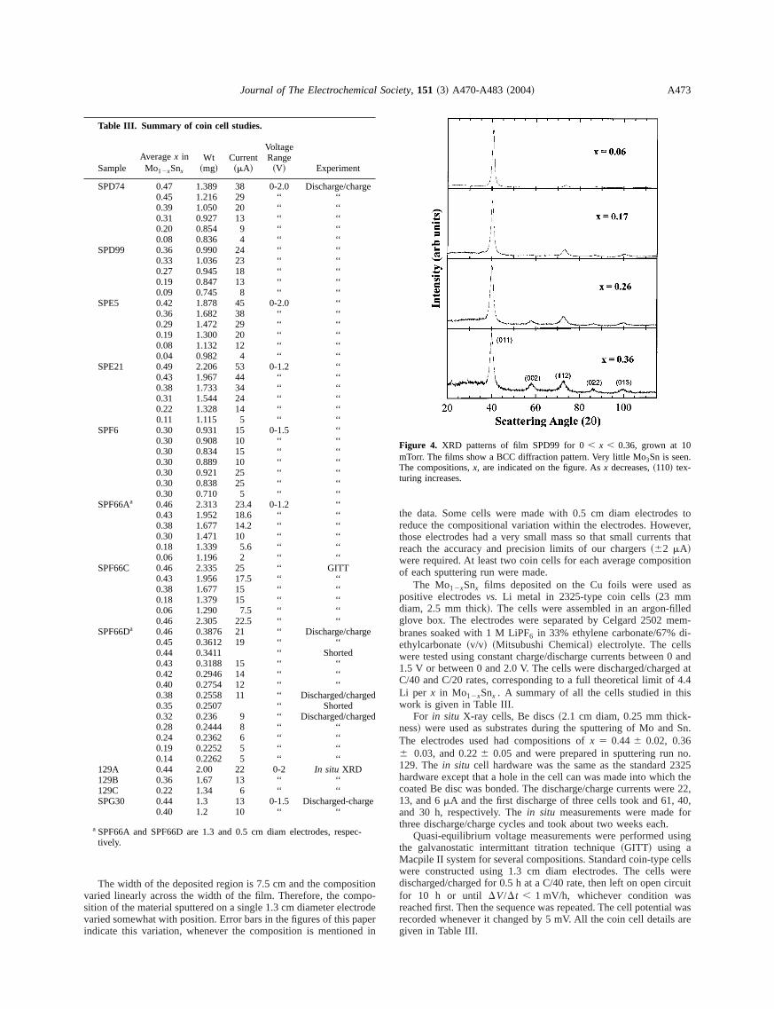
Figure 4. XRD patterns of film SPD99 for 0, x , 0.36, grown at 1mTorr. The films show a BCC diffraction pattern. Very little Mo3Sn is seenThe compositions,x, are indicated on the figure. Asx decreases,~110! tex-turing increases.
t in atwo
ternsre-
d in
for-
x-edstabl
eapid
thed toost-
mi-n issuchsureimilars suther-
Cbe-
wder.gly
theasr Mo
of
n ofringhut the
dif-
ed inV andharge
e,V
ntentide,
-lmse tostant
arge
harge
ities of
ide.of the
Journal of The Electrochemical Society, 151 ~3! A470-A483 ~2004!A474
Results and Discussion
Figure 1 shows the combinatorial mapping of Mo12xSnx for 0, x , 1 from the sputtering run SPD103~Tables I and II!. Theentire compositional range of the binary system is mapped ousingle sputtering experiment. This experiment was made usingopposing linear deposition masks. Figure 2 shows XRD patcollected at various points on the film. Various crystallographicgions of the film are clearly observed in Fig. 2 and describeTable II.
Previously we described the effect of growth conditions onmation of nanocrystalline BCC Mo12xSnx , crystalline BCCMo12xSnx and Mo31ySn phases.16 The BCC metals, generally ehibit a ~110! orientation, because~110! planes are densely packand this would lower the surface energy. We showed that metasubstitutional solid solutions of both BCC Mo12xSnx andb-tungstenstructured Mo31ySn are obtained by sputtering.16 Mo and Sn havno equilibrium solubility, however energetic sputtering and the rquench rates lead to these solid solutions.
The impact of Ar sputtering pressure on oxygen content inresulting films is shown in Fig. 3. High-pressure depositions tengrow more porous films, which are more susceptible to pdeposition oxidation.16 It is our opinion, based on the electrochecal results to be shown later, that the majority of this oxygebonded to molybdenum. It is essential to analyze for oxygen infilms because it has a large impact, as we will show. The meaments, when repeated on copper foil substrate, reveal samounts of oxygen as the measurements performed on glasstrate showing that the detected oxygen is from the film. Furmore, no evidence of Si is seen in either analysis.
Oxygen-Containing Films
Figure 4 shows XRD results for sample SPD99, Mo12xSnxO0.4
(0.02, x , 0.36). For largex, the samples show broad BCpeaks and the grains within the film exhibit random orientation
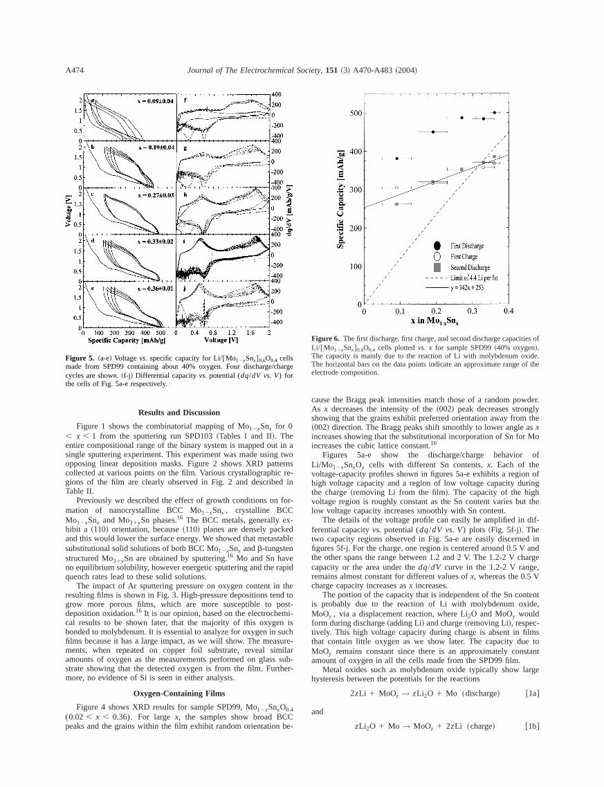
Figure 5. ~a-e! Voltagevs. specific capacity for Li/@Mo12xSnx#0.6O0.4 cellsmade from SPD99 containing about 40% oxygen. Four discharge/ccycles are shown.~f-j ! Differential capacityvs. potential (dq/dV vs. V) forthe cells of Fig. 5a-e respectively.
e
-
b-
cause the Bragg peak intensities match those of a random poAs x decreases the intensity of the~002! peak decreases stronshowing that the grains exhibit preferred orientation away from~002! direction. The Bragg peaks shift smoothly to lower anglexincreases showing that the substitutional incorporation of Sn foincreases the cubic lattice constant.16
Figures 5a-e show the discharge/charge behaviorLi/Mo12xSnxOy cells with different Sn contents,x. Each of thevoltage-capacity profiles shown in figures 5a-e exhibits a regiohigh voltage capacity and a region of low voltage capacity duthe charge~removing Li from the film!. The capacity of the higvoltage region is roughly constant as the Sn content varies blow voltage capacity increases smoothly with Sn content.
The details of the voltage profile can easily be amplified inferential capacityvs. potential (dq/dV vs. V) plots ~Fig. 5f-j!. Thetwo capacity regions observed in Fig. 5a-e are easily discernfigures 5f-j. For the charge, one region is centered around 0.5the other spans the range between 1.2 and 2 V. The 1.2-2 V ccapacity or the area under thedq/dV curve in the 1.2-2 V rangremains almost constant for different values ofx, whereas the 0.5charge capacity increases asx increases.
The portion of the capacity that is independent of the Sn cois probably due to the reaction of Li with molybdenum oxMoOy , via a displacement reaction, where Li2O and MoOy wouldform during discharge~adding Li! and charge~removing Li!, respectively. This high voltage capacity during charge is absent in fithat contain little oxygen as we show later. The capacity duMoOy remains constant since there is an approximately conamount of oxygen in all the cells made from the SPD99 film.
Metal oxides such as molybdenum oxide typically show lhysteresis between the potentials for the reactions
2zLi 1 MoOz → zLi2O 1 Mo ~discharge! @1a#
and
zLi O 1 Mo → MoO 1 2zLi ~charge! @1b#
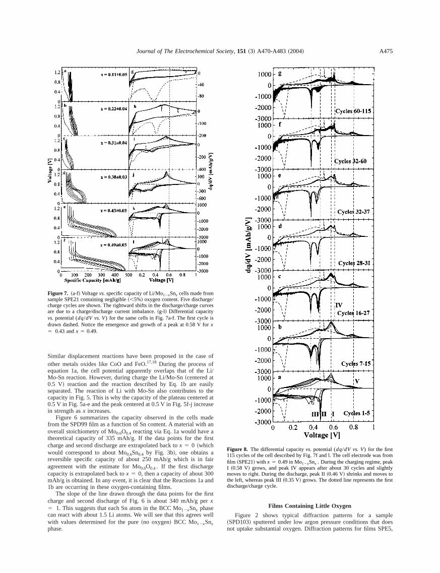
Figure 6. The first discharge, first charge, and second discharge capacLi/ @Mo12xSnx#0.6O0.4 cells plottedvs. x for sample SPD99~40% oxygen!.The capacity is mainly due to the reaction of Li with molybdenum oxThe horizontal bars on the data points indicate an approximate rangeelectrode composition.
2 z
se of
e Li/tasilythe
ed atease
madeana
first
afaire00
and
firstper
well pledoes
PE5,
e/curve
isfor
fromakghtlytofirst
Journal of The Electrochemical Society, 151 ~3! A470-A483 ~2004! A475
Similar displacement reactions have been proposed in the caother metals oxides like CoO and FeO.17,18 During the process oequation 1a, the cell potential apparently overlaps that of thMo-Sn reaction. However, during charge the Li/Mo-Sn~centered a0.5 V! reaction and the reaction described by Eq. 1b are eseparated. The reaction of Li with Mo-Sn also contributes tocapacity in Fig. 5. This is why the capacity of the plateau center0.5 V in Fig. 5a-e and the peak centered at 0.5 V in Fig. 5f-j incrin strength asx increases.
Figure 6 summarizes the capacity observed in the cellsfrom the SPD99 film as a function of Sn content. A material withoverall stoichiometry of Mo0.6O0.4 reacting via Eq. 1a would havetheoretical capacity of 335 mAh/g. If the data points for thecharge and second discharge are extrapolated back tox 5 0 ~whichwould correspond to about Mo0.6Sn0.4 by Fig. 3b!, one obtainsreversible specific capacity of about 250 mAh/g which is inagreement with the estimate for Mo0.6O0.4. If the first dischargcapacity is extrapolated back tox 5 0, then a capacity of about 3mAh/g is obtained. In any event, it is clear that the Reactions 1a1b are occurring in these oxygen-containing films.
The slope of the line drawn through the data points for thecharge and second discharge of Fig. 6 is about 340 mAh/gx5 1. This suggests that each Sn atom in the BCC Mo12xSnx phasecan react with about 1.5 Li atoms. We will see that this agreeswith values determined for the pure~no oxygen! BCC Mo12xSnxphase.
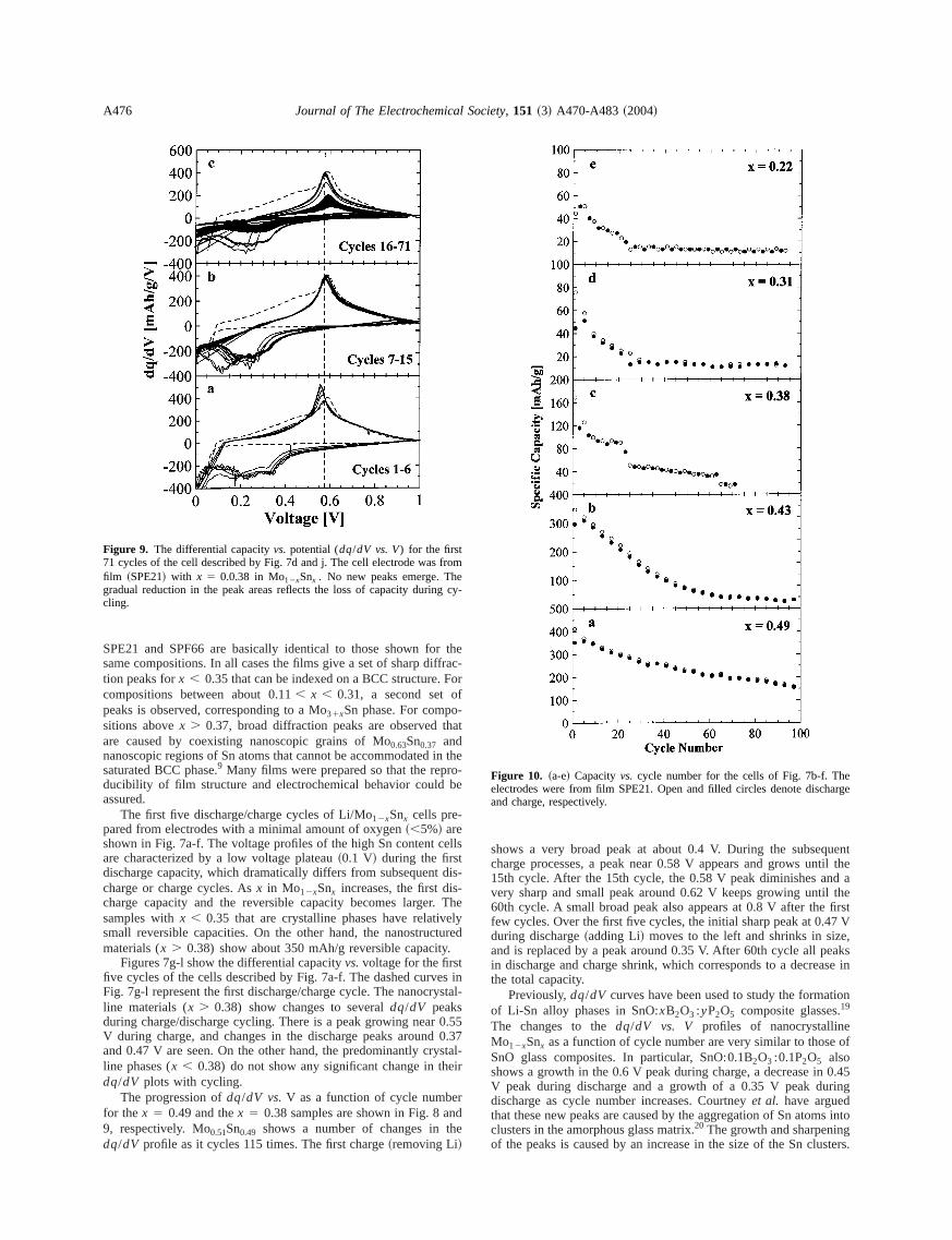
Figure 7. ~a-f! Voltagevs.specific capacity of Li/Mo12xSnx cells made fromsample SPE21 containing negligible~,5%! oxygen content. Five dischargcharge cycles are shown. The rightward shifts in the discharge/chargeare due to a charge/discharge current imbalance.~g-l! Differential capacityvs.potential (dq/dV vs. V) for the same cells in Fig. 7a-f. The first cycledrawn dashed. Notice the emergence and growth of a peak at 0.58 Vx5 0.43 andx 5 0.49.
f
Films Containing Little Oxygen
Figure 2 shows typical diffraction patterns for a sam~SPD103! sputtered under low argon pressure conditions thatnot uptake substantial oxygen. Diffraction patterns for films S
s
Figure 8. The differential capacityvs. potential (dq/dV vs. V) for the first115 cycles of the cell described by Fig. 7f and l. The cell electrode wasfilm ~SPE21! with x 5 0.49 in Mo12xSnx . During the charging regime, peI ~0.58 V! grows, and peak IV appears after about 30 cycles and slimoves to right. During the discharge, peak II~0.46 V! shrinks and movesthe left, whereas peak III~0.35 V! grows. The dotted line represents thedischarge/charge cycle.
r theffrac-For
ofo-that
in thro-be
cellstt dis-s-r. Thvelyture
y.tes inystal
0.550.3
ystaleir
ernd
the
quentntil thend ail the
first47 Ve,eaksase in
tion.ee of
0.45ring
ds into
ngsters.
fromheg cy
heharge
Journal of The Electrochemical Society, 151 ~3! A470-A483 ~2004!A476
SPE21 and SPF66 are basically identical to those shown fosame compositions. In all cases the films give a set of sharp dition peaks forx , 0.35 that can be indexed on a BCC structure.compositions between about 0.11, x , 0.31, a second setpeaks is observed, corresponding to a Mo31xSn phase. For compsitions abovex . 0.37, broad diffraction peaks are observedare caused by coexisting nanoscopic grains of Mo0.63Sn0.37 andnanoscopic regions of Sn atoms that cannot be accommodatedsaturated BCC phase.9 Many films were prepared so that the repducibility of film structure and electrochemical behavior couldassured.
The first five discharge/charge cycles of Li/Mo12xSnx cells pre-pared from electrodes with a minimal amount of oxygen~,5%! areshown in Fig. 7a-f. The voltage profiles of the high Sn contentare characterized by a low voltage plateau~0.1 V! during the firsdischarge capacity, which dramatically differs from subsequencharge or charge cycles. Asx in Mo12xSnx increases, the first dicharge capacity and the reversible capacity becomes largesamples withx , 0.35 that are crystalline phases have relatismall reversible capacities. On the other hand, the nanostrucmaterials (x . 0.38) show about 350 mAh/g reversible capacit
Figures 7g-l show the differential capacityvs.voltage for the firsfive cycles of the cells described by Fig. 7a-f. The dashed curvFig. 7g-l represent the first discharge/charge cycle. The nanocrline materials (x . 0.38) show changes to severaldq/dV peaksduring charge/discharge cycling. There is a peak growing nearV during charge, and changes in the discharge peaks aroundand 0.47 V are seen. On the other hand, the predominantly crline phases (x , 0.38) do not show any significant change in thdq/dV plots with cycling.
The progression ofdq/dV vs.V as a function of cycle numbfor thex 5 0.49 and thex 5 0.38 samples are shown in Fig. 8 a9, respectively. Mo0.51Sn0.49 shows a number of changes indq/dV profile as it cycles 115 times. The first charge~removing Li!
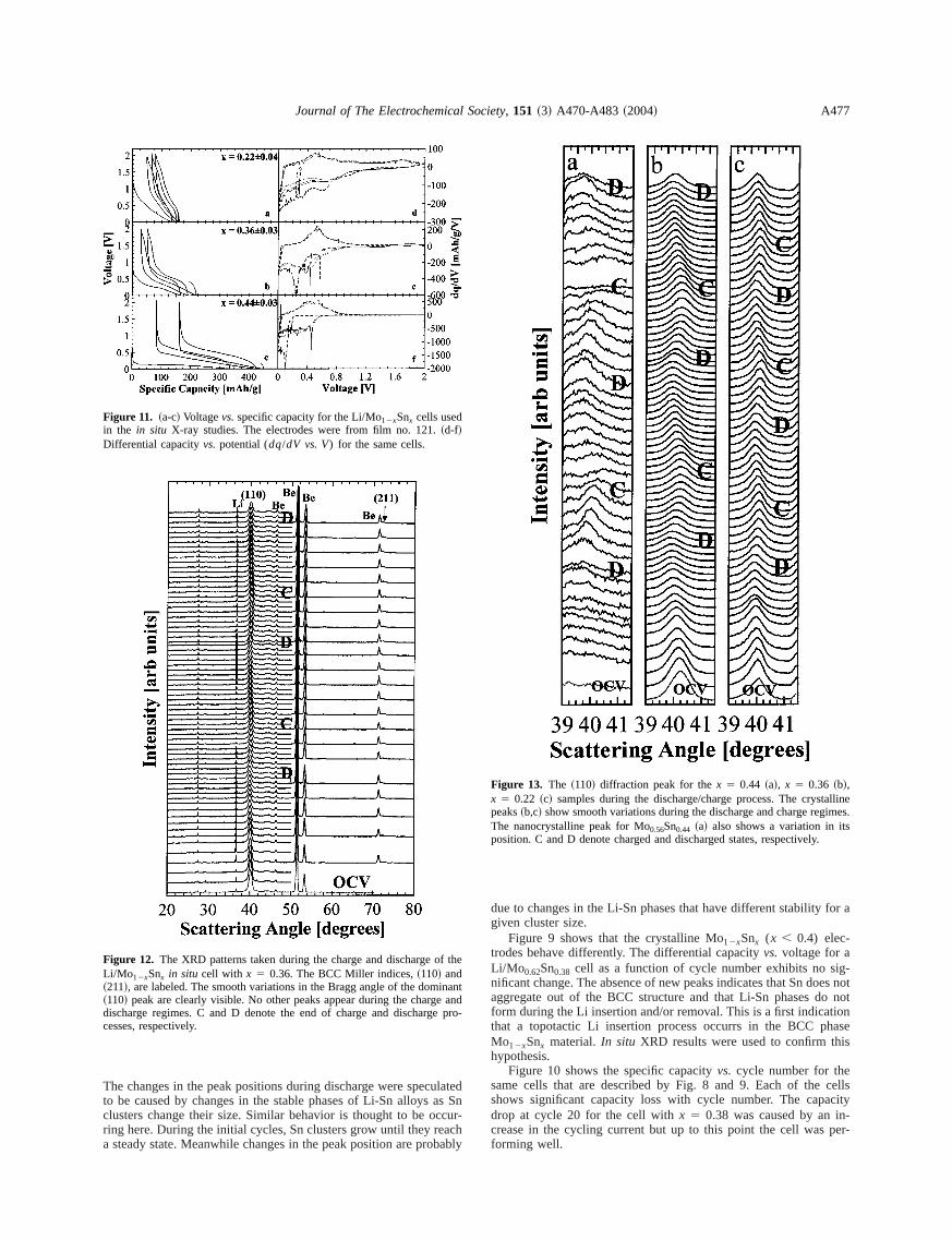
Figure 9. The differential capacityvs. potential (dq/dV vs. V) for the first71 cycles of the cell described by Fig. 7d and j. The cell electrode wasfilm ~SPE21! with x 5 0.0.38 in Mo12xSnx . No new peaks emerge. Tgradual reduction in the peak areas reflects the loss of capacity durincling.
e
e
d
-
7-
shows a very broad peak at about 0.4 V. During the subsecharge processes, a peak near 0.58 V appears and grows u15th cycle. After the 15th cycle, the 0.58 V peak diminishes avery sharp and small peak around 0.62 V keeps growing unt60th cycle. A small broad peak also appears at 0.8 V after thefew cycles. Over the first five cycles, the initial sharp peak at 0.during discharge~adding Li! moves to the left and shrinks in sizand is replaced by a peak around 0.35 V. After 60th cycle all pin discharge and charge shrink, which corresponds to a decrethe total capacity.
Previously,dq/dV curves have been used to study the formaof Li-Sn alloy phases in SnO:xB2O3 :yP2O5 composite glasses19
The changes to thedq/dV vs. V profiles of nanocrystallinMo12xSnx as a function of cycle number are very similar to thosSnO glass composites. In particular, SnO:0.1B2O3 :0.1P2O5 alsoshows a growth in the 0.6 V peak during charge, a decrease inV peak during discharge and a growth of a 0.35 V peak dudischarge as cycle number increases. Courtneyet al. have arguethat these new peaks are caused by the aggregation of Sn atomclusters in the amorphous glass matrix.20 The growth and sharpeniof the peaks is caused by an increase in the size of the Sn clu
-
Figure 10. ~a-e! Capacityvs. cycle number for the cells of Fig. 7b-f. Telectrodes were from film SPE21. Open and filled circles denote discand charge, respectively.
ulateas Sccur-achbabl
for a
-
ig-es noto nottionhaseis
ecells
acityin-per-
f the
inante ande pro
tallineimes.ts.
Journal of The Electrochemical Society, 151 ~3! A470-A483 ~2004! A477
The changes in the peak positions during discharge were specto be caused by changes in the stable phases of Li-Sn alloysclusters change their size. Similar behavior is thought to be oring here. During the initial cycles, Sn clusters grow until they rea steady state. Meanwhile changes in the peak position are pro
Figure 11. ~a-c! Voltagevs.specific capacity for the Li/Mo12xSnx cells usedin the in situ X-ray studies. The electrodes were from film no. 121.~d-f!Differential capacityvs.potential (dq/dV vs. V) for the same cells.
Figure 12. The XRD patterns taken during the charge and discharge oLi/Mo12xSnx in situ cell with x 5 0.36. The BCC Miller indices,~110! and~211!, are labeled. The smooth variations in the Bragg angle of the dom~110! peak are clearly visible. No other peaks appear during the chargdischarge regimes. C and D denote the end of charge and dischargcesses, respectively.
dn
y
due to changes in the Li-Sn phases that have different stabilitygiven cluster size.
Figure 9 shows that the crystalline Mo12xSnx (x , 0.4) electrodes behave differently. The differential capacityvs.voltage for aLi/Mo0.62Sn0.38 cell as a function of cycle number exhibits no snificant change. The absence of new peaks indicates that Sn doaggregate out of the BCC structure and that Li-Sn phases dform during the Li insertion and/or removal. This is a first indicathat a topotactic Li insertion process occurrs in the BCC pMo12xSnx material.In situ XRD results were used to confirm thhypothesis.
Figure 10 shows the specific capacityvs. cycle number for thsame cells that are described by Fig. 8 and 9. Each of theshows significant capacity loss with cycle number. The capdrop at cycle 20 for the cell withx 5 0.38 was caused by ancrease in the cycling current but up to this point the cell wasforming well.
-
Figure 13. The ~110! diffraction peak for thex 5 0.44 ~a!, x 5 0.36 ~b!,x 5 0.22 ~c! samples during the discharge/charge process. The cryspeaks~b,c! show smooth variations during the discharge and charge regThe nanocrystalline peak for Mo0.56Sn0.44 ~a! also shows a variation in iposition. C and D denote charged and discharged states, respectively
film
d
cellssrgedataFig.
eter..
-xpan-isndingg itsthe
s are
ptLihe3 andevers-
w peshar
e anddischarge processes, respectively.
r-
e pro
f thed
chargerespec-
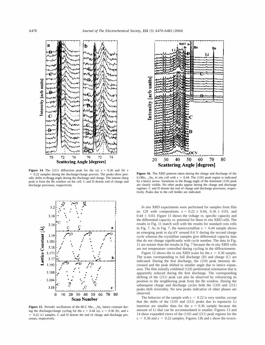
Journal of The Electrochemical Society, 151 ~3! A470-A483 ~2004!A478
In situ XRD experiments were performed for samples fromno 129 with compositions x5 0.226 0.04, 0.366 0.03, and0.446 0.03. Figure 11 shows the voltagevs. specific capacity anthe differential capacityvs.potential for thesein situ XRD cells. Theresults in Fig. 11 match well with the results for standard coinin Fig. 7. As in Fig. 7, the nanocrystallinex 5 0.44 sample showan emerging peak indq/dV around 0.6 V during the second chacycle whereas the crystalline samples give differential capacitythat do not change significantly with cycle number. The data in11 are noisier than the results in Fig. 7 because thein situ XRD cellsare not temperature controlled during cycling in the diffractom
Figure 12 shows thein situ XRD scans for thex 5 0.36 sampleThe scans corresponding to full discharge~D! and charge~C! areindicated. During the first discharge, the~110! peak intensity decreased and the peak shifted to smaller angle due to lattice esion. The film initially exhibited~110! preferential orientation thatapparently reduced during the first discharge. The corresposhifting of the ~211! peak can also be observed by referencinposition to the neighboring peak from the Be window. Duringsubsequent charge and discharge cycles both the~110! and ~211!peaks shift reversibly. No new peaks indicative of other phaseobserved.
The behavior of the sample withx 5 0.22 is very similar, excethat the shifts of the~110! and ~211! peaks due to topotacticinsertion are smaller than for thex 5 0.36 sample because tamount of Li that can be accommodated is smaller. Figures 114 show expanded views of the~110! and~211! peak regions for thx 5 0.36 andx 5 0.22 samples. Figures 13b and c show the re
ri-p
-
Figure 16. The XRD patterns taken during the charge and discharge oLi/Mo12xSnx in situ cell with x 5 0.44. The~110! peak region is indicateby a heavy arrow. Variations in the Bragg angle of the dominant~110! peakare clearly visible. No other peaks appear during the charge and disregimes. C and D denote the end of charge and discharge processes,tively. Peaks due to the cell holder are indicated.
Figure 14. The ~211! diffraction peak for the~a! x 5 0.36 and ~b! x5 0.22 samples during the discharge/charge process. The peaks sho
odic shifts in Bragg angle during the discharge and charge. The intensepeak is from the Be window on the cell. C and D denote end of charg
Figure 15. Periodic oscillations of the BCC Mo12xSnx lattice constant duing the discharge/charge cycling for thex 5 0.44 ~a!, x 5 0.36 ~b!, andx5 0.22 ~c! samples. C and D denote the end of charge and dischargcesses, respectively.
iftingc-
con-ggFig.
nsttice
finiteof
lec-of thn conofate.
nd
patdpeaky the
fromareiffrace po15a
theal site
oms-n-
tered cubic phase, presumably a molybdenum suboxide is observed.
h
Journal of The Electrochemical Society, 151 ~3! A470-A483 ~2004! A479
ible shifting of the ~110! peak for thex 5 0.36 andx 5 0.22samples respectively. Figures 14a and b show the reversible shof the ~211! peak for thex 5 0.36 andx 5 0.22 samples, respetively.
The lattice constants of the BCC phase as a function of Litent were obtained from the~110! scattering angle using the Bralaw and are shown as a function of the X-ray scan number in15b and c for thex 5 0.36 andx 5 0.22 samples. The oscillatioin the lattice parameter are periodic and show that the BCC laexpands/shrinks during Li insertion/removal. We take this as deevidence for the topotactic insertion of Li into interstitial sitesBCC Mo12xSnx . There is some off-axis displacement of the etrode with respect to the goniometer center so the exact valueslattice parameters may be systematically off, because higher Stent samples have larger lattice constant.15 However, the changesthe lattice constants with state-of-charge are considered accur
In situ XRD studies were also made on thex 5 0.44 samplefrom film no. 129. This material is initially nanocrystalline ashows a diffraction pattern much like that in Fig. 2 for thex5 0.51 sample. Figure 16 shows the changes to the diffractiontern that occur as the Li/Mo0.56Sn0.44 cell is sequentially dischargeand charged. Since the electrode is nanocrystalline the Braggfrom the electrode material are broad and we had to magnifintensity scale to observe them. This means that weak peakscell parts below 30° that were difficult to observe in Fig. 12,more easily observed here. Furthermore the changes to the dtion pattern are much harder to interpret. Figure 13a shows thsition ~110! peak region as a function of state of charge. Figure
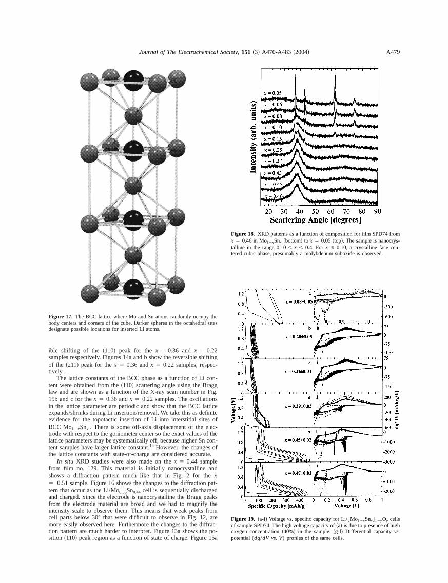
Figure 17. The BCC lattice where Mo and Sn atoms randomly occupybody centers and corners of the cube. Darker spheres in the octahedrdesignate possible locations for inserted Li atoms.
Figure 18. XRD patterns as a function of composition for film SPD74 frx 5 0.46 in Mo12xSnx ~bottom! to x 5 0.05 ~top!. The sample is nanocrytalline in the range 0.10, x , 0.4. Forx < 0.10, a crystalline face ce
e-
-
s
--
s
Figure 19. ~a-f! Voltagevs.specific capacity for Li/@Mo12xSnx#12yOy cellsof sample SPD74. The high voltage capacity of~a! is due to presence of higoxygen concentration~40%! in the sample.~g-l! Differential capacityvs.potential (dq/dV vs. V) profiles of the same cells.
-andto th
e tharinghatof ther-ter-ro-
o in-, the
with
ies ofrstand
udiedernsosi-
neange-face
m
oxy-orpo-tion.bde-t-
19.
roms-
Journal of The Electrochemical Society, 151 ~3! A470-A483 ~2004!A480
shows the lattice constant derived from the~110! peak position plotted vs. X-ray scan number with the positions of full dischargecharge indicated. Again, there appear to be reversible changeslattice.
Based on the results in Fig. 13, 14, 15, and 16, we assumreversible topotactic insertion of Li into interstitial sites is occurin these BCC Mo12xSnx samples. What are the interstitial sites tmight be involved? The octahedral sites located at the centerfaces of the conventional BCC unit cell~Fig. 17! are possible intestitial sites for Li atoms. Hydrogen has shown to insert in the institial sites of BCC metals like Nb. Alpha-NbH contains two hydgen atoms per BCC subcell tetrahedrally bonded to Nb.20
The nanocrystalline materials are certainly more complex tterpret than the crystalline BCC phases. As shown before
Figure 20. Capacityvs. cycle number for the cells described by Fig.Open and filled circles denote discharge and charge, respectively.
e
t
dq/dV patterns show aggregation of Sn into larger clusterscycle number, howeverin situ XRD patterns for thex 5 0.44sample show no new peaks in the first three cycles. X-ray studelectrodes cycled for tens of cycles are needed to help undethe changes to the electrode structure with cycling.
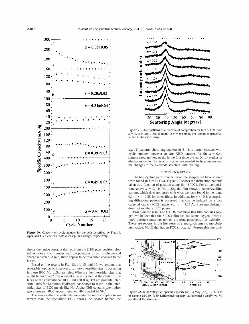
Film SPD74, SPG30
The best cycling performance for all the samples we have stwere found in film SPD74. Figure 18 shows the diffraction patttaken as a function of position along film SPD74. For all comptions abovex 5 0.1 in Mo12xSnx the film shows a nanocrystallipattern, which does not agree with what we have found in the r0.1 , x , 0.38 for other films. In addition, forx , 0.1, a surprising diffraction pattern is observed that can be indexed on acentered cubic~FCC! lattice with a5 4.15 Å. Pure molybdenudoes not exhibit a FCC phase.
Based on the results of Fig. 3b that show this film containsgen, we believe that the SPD74 film has had some oxygen incrated during sputtering, not only during postdeposition oxidaThere are reports in the literature of a substoichiometric molynum oxide, Mo3O that has an FCC structure.21 Presumably the spu
Figure 21. XRD patterns as a function of composition for film SPG30 fx 5 0.42 in Mo12xSnx ~bottom! to x 5 0.1 ~top!. The sample is nanocrytalline in the entire range.
Figure 22. ~a-b! Voltagevs.specific capacity for Li/@Mo12xSnx#12yOy cellsof sample SPG30.~c-d! Differential capacityvs. potential (dq/dV vs. V)profiles of the same cells.
r ofntly,turbs-. 184.nnotll the.tainins
ngitysultsowand
hasregaouldof
glaselpsacityatri
osi-n
cubicenygen-rich
hout
n of
files
er Spaci-lline
clus-withnoharge
les isngck-ess ofs in
a
on ofn ofhad
PG30into
rther
dtxida-s thehad
icate
.
thoundre-rface.
Journal of The Electrochemical Society, 151 ~3! A470-A483 ~2004! A481
tering was made under conditions involving a small leak of air otarget cooling water and this has led to this material. Appareaccording to this hypothesis, the incorporated oxygen also disthe formation of the crystalline BCC phase forx . 0.1, and nanocrystalline materials are formed. A close examination of Figshows the growth of a shoulder near 31° asx increases above 0.This shoulder is due to diffraction from nanoscopic Sn that cabe incorporated in the solid-solution phase. We believe that acompositions in film SPD74 contain some incorporated oxygen
Figure 19 shows the charge/discharge behavior of cells coning the SPD74 films. All these cells with nanocrystalline grashow smoothdq/dV vs.V curves with no emerging peaks durithe entire 20 cycles, even forx . 0.4. Figure 20 shows the capacvs.cycle number for the same cells. Most interesting are the refor x 5 0.45 andx 5 0.47. The cells with these electrodes shsmall irreversible capacity, little capacity loss over 20 cyclesspecific capacities near 350 mAh/g.
We believe that presence of 20% oxygen in the SPD74 filmhelped to stabilize the nanocrystalline structure against Sn aggtion and the subsequent formation of LiSn phases, which wnormally limit the cycling capability of the material. In the caseSnO glass composites, it has been shown that more(B2O3 :P2O5) in the composite retards the clustering of Sn and hto improve the cycling life. It has also been suggested that capfade can be avoided if Sn particles are imbedded in a reduced mMoOx , wherex , 1.22
To investigate the effect of oxygen during the growth, a deption experiment~SPG30! with similar sputtering conditions to ruSPD74 was performed. In this run, gas flows of 3.5 standardcentimeters per minute~sccm! of argon, and 0.5 sccm of oxygwere used. The total pressure was about 3.5 mTorr. The oxconcentration in the film increases from about 10% at the Snend of the film to about 50% in the Mo end~Fig. 3c!. The X-raypatterns of the film indicate the nanocrystalline structure througthe composition range of 0.02, x , 0.44 ~Fig. 21!. Thus we wereable to approximately reproduce the structure and compositiothe Mo-Sn films made in run SPD74.
The voltage-capacity and differential capacity-potential proof the ~SPG30! films are shown in Fig. 22 forx 5 0.40 andx5 0.44. These are the interesting compositions because lowcontent films have lower capacities, and higher irreversible caties. As was the case in the oxygen-containing nanocrystaSPD74 cells, the SPG30 cells show almost no formation of Snters. The differential capacity profiles of the SPG30 samplesx 5 0.40 andx 5 0.44 are very similar to those of SPD74:significant 0.6 and 0.35 V peaks appear during charge and disc
Figure 23. Capacityvs.cycle number for the cells described by Fig. 22
-
-
s
x
n
,
respectively. However, the capacity retention for these samprelativley poor~Fig. 23!. The initial increase in the capacity durithe first few cycles is attributed cracking of the film. During craing, new surfaces are presumably exposed, allowing better accthe Li ions to the electrode. After about 15 cycles a rapid loscapacity is observed. A closer look at the differential capacityvs.potential for thex 5 0.40 andx 5 0.44 samples reveals onlyslight growth of a 0.6 V peak during the charge~Fig. 24!. We believethat for these cells, the loss in capacity is due to the delaminatithe film from the substrate during repeated cycling. An inspectiothe cells after 50 cycles showed that almost all of the filmdelaminated from the copper substrate.
It is clear that the presence of oxygen in the SPD74 and Sfilms has a dramatic effect on the rate of aggregation of Snlarger clusters. It is our opinion that this effect deserves fustudy.
Summary of Specific Capacityvs. x in Mo12xSnx for All FilmsExcept SPD99
Figure 25 shows the specific capacity plottedvs. x in Mo12xSnxfor the first discharge~Fig. 25a!, first charge~Fig. 25b! and secondischarge~Fig. 25c! of Li/Mo12xSnx cells. All of the films excepSPD99, that had large oxygen content due to postdeposition otion, have been included. The dashed line in each panel showspecific capacity that would have been attained if each Sn atomreacted with 4.2 Li atoms. The bold arrows in the figures ind
Figure 24. ~a,c! Differential capacityvs. potential (dq/dV vs. V) of theSPG30 cells withx 5 0.44 andx 5 0.40 for the first 15 cycles. The growof the 0.6 V peak during charge is significantly retarded. No peak ar0.35 V appears during discharge.~b,d! Further cycles show a dramaticduction in the capacity due to poor adhesion at the film/substrate inte
tedtheesitione
c-asesset
nowions.re-
t the
t theal-les.sured-10 hrentby thereactwithma-efor-It isquitehee aiffer-
rizontal barsto the ey
ner re-
Journal of The Electrochemical Society, 151 ~3! A470-A483 ~2004!A482
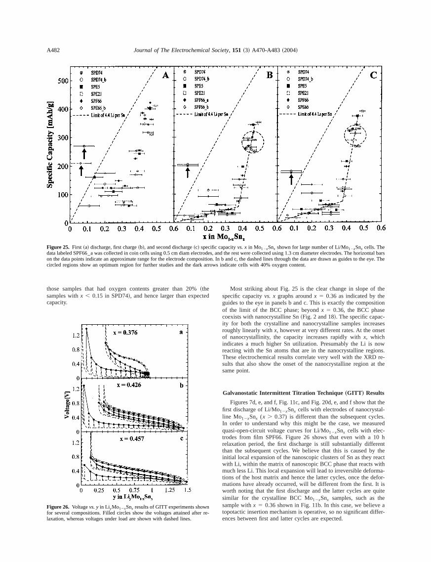
those samples that had oxygen contents greater than 20%~thesamples withx , 0.15 in SPD74!, and hence larger than expeccapacity.
Figure 25. First ~a! discharge, first charge~b!, and second discharge~c! specdata labeled SPF66–a was collected in coin cells using 0.5 cm diam electon the data points indicate an approximate range for the electrode comcircled regions show an optimum region for further studies and the da
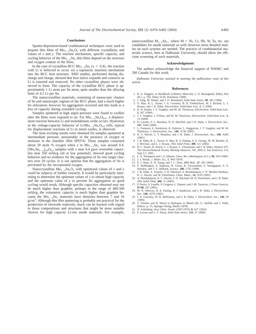
Figure 26. Voltagevs. yin Li yMo12xSnx results of GITT experiments showfor several compositions. Filled circles show the voltages attained aftlaxation, whereas voltages under load are shown with dashed lines.
Most striking about Fig. 25 is the clear change in slope ofspecific capacityvs. xgraphs aroundx 5 0.36 as indicated by thguides to the eye in panels b and c. This is exactly the compoof the limit of the BCC phase; beyondx 5 0.36, the BCC phascoexists with nanocrystalline Sn~Fig. 2 and 18!. The specific capaity for both the crystalline and nanocrystalline samples increroughly linearly withx, however at very different rates. At the onof nanocrystallinity, the capacity increases rapidly withx, whichindicates a much higher Sn utilization. Presumably the Li isreacting with the Sn atoms that are in the nanocrystalline regThese electrochemical results correlate very well with the XRDsults that also show the onset of the nanocrystalline region asame point.
Galvanostatic Intermittent Titration Technique „GITT … Results
Figures 7d, e, and f, Fig. 11c, and Fig. 20d, e, and f show thafirst discharge of Li/Mo12xSnx cells with electrodes of nanocrystline Mo12xSnx (x . 0.37) is different than the subsequent cycIn order to understand why this might be the case, we meaquasi-open-circuit voltage curves for Li/Mo12xSnx cells with electrodes from film SPF66. Figure 26 shows that even with arelaxation period, the first discharge is still substantially diffethan the subsequent cycles. We believe that this is causedinitial local expansion of the nanoscopic clusters of Sn as theywith Li, within the matrix of nanoscopic BCC phase that reactsmuch less Li. This local expansion will lead to irreversible defortions of the host matrix and hence the latter cycles, once the dmations have already occurred, will be different from the first.worth noting that the first discharge and the latter cycles aresimilar for the crystalline BCC Mo12xSnx samples, such as tsample withx 5 0.36 shown in Fig. 11b. In this case, we believtopotactic insertion mechanism is operative, so no significant dences between first and latter cycles are expected.
apacityvs. xin Mo12xSnx shown for large number of Li/Mo12xSnx cells. The, and the rest were collected using 1.3 cm diameter electrodes. The hoon. In b and c, the dashed lines through the data are drawn as guidese. Theows indicate cells with 40% oxygen content.
ific crodespositirk arr
ed t
andre
nismdis-acts
ob-ap-
ying
stersigheto a
xidize-resis
l
ed aen oed.ci-gclus-n is
nter-yodnot-500be-10
thegard
itable
estud-
al ma-effi-
and
f this
art
. J.
tt.,
.,
M. M.
t, D.
t 257,, CA,
, E. S.
haus,
ahn,
s,
.
,
Journal of The Electrochemical Society, 151 ~3! A470-A483 ~2004! A483
Conclusions
Sputter-deposition-based combinatorial techniques were usprepare thin films of Mo12xSnxOy with different crystallinity andvalues ofx and y. The reaction mechanism, specific capacity,cycling behavior of the Mo12xSnx thin films depend on the structuand oxygen content of the films.
In the case of crystalline BCC Mo12xSnx (x , 0.4), the reactiowith Li is believed to occur via a topotactic insertion mechaninto the BCC host structure. XRD studies, performed duringcharge and charge, showed that host lattice expands and contrLi is inserted and removed. No other crystalline phases wereserved to form. The capacity of the crystalline BCC phase isproximately 1 Li atom per Sn atom, quite smaller than the allolimit of 4.2 Li per Sn.
The nanocrystalline materials, consisting of nanoscopic cluof Sn and nanoscopic regions of the BCC phase, had a much hSn utilization; however Sn aggregation occurred and this leadsloss of capacity during extended cycling.
Samples sputtered at high argon pressure were found to oafter the films were exposed to air. For Mo12xSnxO0.4, a displacement reaction between Li and molybdenum oxide occurs. Hystein the voltage-capacity behavior of Li/Mo12xSnxO0.4 cells, typicafor displacement reactions of Li in metal oxides, is observed.
The most exciting results were obtained for samples sputterintermediate pressure, presumably in the presence of oxygmoisture in the chamber~film SPD74!. These samples containabout 20 atom % oxygen whenx in Mo12xSnx was around 0.4@MoxSn12x#0.8O0.2 samples withx near 0.4 gave reversible capaties near 350 mAh/g~all at low potential!, showed good cyclinbehavior and no evidence for the aggregation of Sn into largerters over 20 cycles. It is our opinion that the aggregation of Sprevented by the incorporated oxygen.
Nanocrystalline Mo12xSnxOy with optimized values ofx and ycould be subjects of further research. It would be particularly iesting to determine the optimum values ofx to obtain high capacitand the optimum value ofy to prevent Sn aggregation so gocycling would result. Although specific capacities obtained maybe much higher than graphite, perhaps in the range of 400mAh/g, the volumetric capacity is much higher than graphitecause the Mo12xSnx materials have densities between 7 andg/cm3. Although thin film sputtering is probably not practical forproduction of electrode materials, much can be learned with reto those compositions and structures that might be more su
choices for high capacity Li-ion anode materials. For example,o
as
r
tr
nanocrystalline M12xSnx , where M5 Ni, Cr, Nb, W, Ta, etc. arcandidates for anode materials as well; however more detailedies on such systems are needed. The practice of combinatoriterials science, here at Dalhousie University, should allow thecient screening of such materials.
Acknowledgments
The authors acknowledge the financial support of NSERC3M Canada for this work.
Dalhousie University assisted in meeting the publication costs oarticle.
References
1. R. A. Huggins, inHandbook of Battery Materials, J. O. Besenghard, Editor, PIII.1, p. 359, Wiley-VCH, Wienheim~1999!.
2. J. Yang, M. Winter, and J. O. Besenhard,Solid State Ionics,90, 281 ~1996!.3. O. Mao, R. L. Turner, I. A. Courtney, B. D. Fredericksen, M. I. Buckett, L
Krause, and J. R. Dahn,Electrochem. Solid-State Lett.,2, 3 ~1999!.4. K. D. Kepler, J. T. Vaughey, and M. M. Thackeray,Electrochem. Solid-State Le
2, 307 ~1999!.5. J. T. Vaughey, J. O’Hara, and M. M. Thackeray,Electrochem. Solid-State Lett.,3,
13 ~2000!.6. D. Larcher, Y. L. Beaulieu, D. D. MacNeil, and J. R. Dahn,J. Electrochem. Soc
147, 1658~2000!.7. L. Fransson, E. Nordstrom, K. Edstrom, L. Haggstrom, J. T. Vaughey, and
Thackeray,J. Electrochem. Soc.,149, A736 ~2002!.8. K. C. Hewitt, L. Y. Beaulieu, and J. R. Dahn,J. Electrochem. Soc.,148, A402
~2001!.9. J. R. Dahn, R. L. Turner, O. Mao, R. A. Dunlap, A. E. George, M. M. Bucket
J. McClure, and L. J. Krause,Thin Solid Films,408, 111 ~2002!.10. R. L. Turner, B. Amick, L. J. Krause, L. Christensen, and J. R. Dahn, Abstrac
The Electrochemical Society Meeting Abstracts, Vol. 2001-2, San FranciscoSept 2-7, 2001.
11. L. A. Thompson and J. A. Ellman,Chem. Rev. (Washington, D.C.),96, 550~1996!.12. J. J. Hanak,J. Mater. Sci.,5, 964 ~1970!.13. E. J. Amis, X. D. Xiang, and J. C. Zhao,MRS Bull.,27, 295 ~2002!.14. E. Reddington, A. Sapienza, B. Gurau, R. Viswanathan, S. Sarangapani
Smotkin, and T. E. Mallouk,Science,280, 1735~1998!.15. J. R. Dahn, S. Trussler, T. D. Hatchard, A. Bonakdarpour, J. N. Meuller-Neu
K. C. Hewitt, and M. Fleischauer,Chem. Mater.,14, 3519~2002!.16. A. Bonakdarpour, K. C. Hewitt, T. D. Hatchard, M. D. Fleischauer, and J. R. D
Thin Solid Films,440, 11 ~2003!.17. P. Poizot, S. Lauelle, S. Grugeon, L. Dupont, and J.-M. Tarascon,J. Power Source
97-98, 235 ~2001!.18. M. N. Obrovac, R. A. Dunlap, R. J. Sanderson, and J. R. Dahn,J. Electrochem
Soc.,148, A576 ~2001!.19. I. A. Courtney, W. R. McKinnon, and J. R. Dahn,J. Electrochem. Soc.,146, 59
~1999!.20. T. Schober and H. Wenzl inHydrogen in Metals (II), G. Alefeld, and J. Volkl
Editors, p. 15, Springer-Verlag, Berlin~1978!.21. N. Scho¨nberg,Acta Chem. Scand. (1947-1973),8, 617 ~1954!.
22. F. Leroux and L. F. Nazar,Solid State Ionics,133, 37 ~2000!.