Embed Size (px)
Citation preview
Electrochemical and surface characterization of platinum silicideelectrodes and their use as stable platforms for electrogenerated
chemiluminescence assays
Eve F. Fabrizio, Todd M. McEvoy, Priya Jassel, Jose Lozano, Keith J. Stevenson,Allen J. Bard *
Department of Chemistry and Biochemistry, University of Texas at Austin, Austin, TX 78712, USA
Received 21 October 2002; received in revised form 10 January 2003; accepted 20 January 2003
Journal of Electroanalytical Chemistry 554�/555 (2003) 99�/111
www.elsevier.com/locate/jelechem
Abstract
Electrochemical methods, including cyclic voltammetry and scanning electrochemical microscopy, as well as surface techniques,
including conductive atomic force microscopy (AFM) and X-ray photoelectron spectroscopy, were utilized to evaluate and
characterize the extent of an oxide layer on platinum silicide (PtSi) surfaces that were pretreated by a variety of approaches; piranha
solution (1:4 H2O2�/H2SO4), hydrofluoric acid (HF), chemical reduction in NaBH4 and after mechanically polishing the surface.
Electrochemical methods showed that in the presence of an oxide layer, the rate of electron transfer depended upon the charge of the
redox couple: the more negative the charge, the slower is the rate of electron transfer. Additionally, the current levels observed in the
presence of an extensive oxide layer were considerably lower than those observed after the oxide layer was removed either with HF
acid or by mechanically polishing. Surface analysis and depth profiles obtained using Auger electron spectroscopy demonstrated
that PtSi surfaces pretreated with piranha contained the largest amounts of surface oxides. AFM topographic scans along with
localized surface conductivity showed that in the presence of this oxide layer, electron transfer occurred at nanoscale domains
located between the PtSi grains with the rest of the surface, which most likely contains an oxide layer, being non-conductive. The
surface oxide layer was used to attach the electrogenerated chemiluminescent (ECL) label, Ru(bpy)32� covalently, either directly or
via single-stranded DNA. Emission during oxidation in the presence of the co-reactant tri-n -propylamine was observed, illustrating
the possible use of PtSi as a platform for ECL-based bioassays.
# 2003 Elsevier Science B.V. All rights reserved.
Keywords: Platinum silicide; Disk electrodes; Charge transfer kinetics; Electroluminescence
1. Introduction
Silicides are of great interest as low-cost stable
materials for solid-state microelectronics and as radia-
tion detectors [1�/6]. In particular, by incorporating
noble metals such as platinum into silicon, the poly-
silicon interconnect resistance can be reduced, therefore,
providing low-resistance ohmic contacts for transistors.
As device dimensions reach the sub-micron range, one
must determine whether electrical and mechanical
integrity of the silicide is maintained. As a result,
numerous studies have characterized the kinetics of
phase formation, final composition, microstructure
and electron structure of sub-half micron thin platinum
silicide (PtSi) films. Additionally, PtSi has been studied
as an alternative electrode for hydrogen evolution and
water electrolysis [7�/9]. Even though previous studies by
these groups have centered on obtaining enhanced rates
of electrolysis, they also evaluated structural stability
with extreme potential biasing. PtSi has also been used
to protect Si electrodes in photoelectrochemical cells,
even allowing the photogeneration of chlorine [10,11].
Overall, PtSi has been shown to possess electrical and
chemical properties that are similar to those of pure
platinum: low resistivity and nominal corrosion during
electrolysis. It is these physical properties, along with the
* Corresponding author. Tel.: �/1-512-471-3761; fax: �/1-512-471-
0088.
E-mail address: [email protected] (A.J. Bard).
0022-0728/03/$ - see front matter # 2003 Elsevier Science B.V. All rights reserved.
doi:10.1016/S0022-0728(03)00112-8
possibility of having a surface oxide layer, which make
PtSi a workable material for use as array electrodes in
electrophoretic microdevices and electrochemical bio-
sensors.While a small number of studies has evaluated the
current vs. voltage curves of PtSi in aqueous electrolytes,
none of these studies has closely evaluated the electro-
chemical properties of this alloy, specifically, the hetero-
geneous electron transfer observed at the surface of
these films [12�/14]. Previous surface analysis and depth
profiling obtained using a variety of X-ray photoelec-
tron spectroscopy (XPS) methods have determined thatPtSi annealed in a conventional furnace contains a
three-layer structure, a top monolayer of atomic Pt and
SiO2, an underlying monolayer of PtxSiy (where x �/y),
and a bulk layer of PtSi [15�/26]. All three layers vary in
structure and thickness based on the annealing condi-
tions; atmosphere, temperature, and time [15]. The goal
of this work was to investigate the electrochemical
properties of PtSi after a number of standard pretreat-ments to determine the viability of PtSi films for future
use in electrochemical microdevices and sensors. In
particular, we were interested in using surface-sensitive
electrochemical methods, such as cyclic voltammetry
(CV) and scanning electrochemical microscopy
(SECM), in addition to surface techniques, such as
Auger electron spectroscopy (AES) and conductive
atomic force microscopy (AFM), to characterize thechemical and electrochemical surface properties of these
films.
2. Experimental
2.1. Chemicals and materials
Platinum silicide (PtSi) wafers were obtained fromNanogen, Inc. (San Diego, CA). The wafers were
prepared by sputtering 500 A of Si and 500 A of Pt at
1000 W under an inert atmosphere onto a plasma-
cleaned oxidized silicon wafer using a Perkin�/Elmer
4480 Production Sputtering System (Perkin�/Elmer,
Ultek Division, Palo Alto, CA). The platinum layer
was then annealed into the silicon layer by heating the
wafers at 420 8C for 30 min in an oxygen-free environ-ment. Piranha solution was prepared by mixing one part
hydrogen peroxide (Mallinckrodt, Paris, KY) to four
parts concentrated sulfuric acid (Mallinckroft, Phillips-
burgh, NJ). (Caution: piranha solution is a very strong
oxidizing agent and very dangerous to handle in the
laboratory. Protective equipment including gloves, gog-
gles, and face shields should be used at all times.)
Hydrofluoric (HF) acid solutions (1%) used for etchingSiO2 were prepared by adding 10 ml of concentrated HF
(48%; EM Sciences, Gibbstown, NJ) to 1 ml of Milli-Q
water (Millipore Corp., Bedford, MA) (extreme care
should be taken when working with HF solutions).
Small volumes (B/1 ml) were prepared to minimize
potential exposure and waste disposal. Sodium tetrahy-
dridoborate (or sodium borohydride (NaBH4); Aldrich,Milwaukee, WI) solutions at a concentration of 1 M
were prepared by dissolving the appropriate weight into
a given volume of Milli-Q water.
2.2. Electrochemical analysis on PtSi surfaces
PtSi wafers were diced or cut into 1 cm�/1 cm size
chips with a diamond scribe. After the PtSi chips werefirst treated with piranha solution, electrical contact was
made to one corner of the PtSi side of the chip using
insulated nichrome-coated copper wire and silver epoxy
(H2OE from EPO-TEK, Billerica, MA). The contact
point was covered with 5 Minute Epoxy (ITW Devon
Corp., Danvers, MA) to ensure that the silver epoxy was
never in contact with the electrolyte during measure-
ments. To verify good electrical contact, the resistancebetween the PtSi surface and the wire was tested with an
ohmmeter. Some of the PtSi surfaces were then addi-
tionally treated by either etching off the SiO layer using
1% HF, reducing the surface with NaBH4 or by
mechanically polishing with 0.05 mm alumina and a
microcloth (Buehler, Lake Bluff, IL). For the HF and
NaBH4 solutions, a small drop was placed onto the
center of the surface of the PtSi surface and left there fora given amount of time: 30 s for 1% HF and 1 min for 1
M NaBH4. All chips were thoroughly rinsed with Milli-
Q water and dried using a high-pressure nitrogen line
prior to any experimental measurement.
To facilitate electrochemical measurement, all PtSi
chips were mounted onto a special glass cell holder that
contained a 3 mm diameter hole (area equal to 0.071
cm2). A front and side image of the cell is provided inFig. 1. Each chip was placed in contact with the
electrolyte solution by positioning it over the hole and
by clamping it into place with a Plexiglas plate that was
held in place by two Teflon screws. A Neoprene o-ring
was positioned between the glass cell and the PtSi
surface to eliminate electrolyte leakage. The rest of the
electrochemical cell consisted of a platinum mesh
counterelectrode and silver j silver chloride referenceelectrode (Ag j AgCl j KCl (sat.)). Prior to obtaining
voltammograms, the PtSi surface was cycled approxi-
mately 40 times in 0.2 M H2SO4 between 0.9 and �/0.3 V
versus Ag j AgCl j KCl (sat.). Voltammetric scans invol-
ving the hydrogen evolution reaction (her) were per-
formed in 1.0 M H2SO4 while the underpotential
deposition (upd) of copper was performed in 0.2 M
H2SO4. All additional voltammetry using a polycrystal-line platinum surface was performed with a 1.5-mm
diameter Pt disk electrode (BioAnalytical Systems,
Indianapolis, IN) that was mechanically polished with
E.F. Fabrizio et al. / Journal of Electroanalytical Chemistry 554�/555 (2003) 99�/111100
0.05 mm alumina and a microcloth (Buehler, Lake Bluff,
IL).
2.3. SECM instrumentation and procedure
The basic experimental set-up used for the SECM
measurements consisted of a CH Instruments 900
SECM (CH Instruments, Austin, TX). After the PtSi
substrates were cleaned and pretreated using the sameprocedures discussed in the above section, they were
mounted into a homemade Teflon SECM cell that
exposed a circular area approximately 2 mm diameter
(area�/0.031 cm2) to facilitate tip access. The probe tip
consisted of a 25-mm diameter Pt disk ultramicroelec-
trode embedded in glass with a total radius of 40 mm.
This corresponds to an RG value (RG�/total radius/
radius of Pt disk) of �/3.5. The reference electrode wasan Ag j AgCl j KCl (sat.) electrode and the counter-
electrode was a Pt wire. Prior to the SECM measure-
ments, the PtSi surface was cycled approximately 40
times in 0.2 M H2SO4 between 0.9 and �/0.3 V versus
Ag j AgCl j KCl (sat.) to be consistent with our voltam-
metric measurements. Using the SECM bipotentiostat,
the electrochemical behavior of both the tip andsubstrates was evaluated by obtaining voltammograms
of the solution redox couple prior to acquiring series of
approach curves. Each approach curve was obtained by
setting the tip to a potential at which a steady-state
response is observed while the potential applied to the
PtSi substrate was varied from approximately 1000 to 0
mV past the E8 depending on the redox couple being
measured. The tip, which was driven by an inchworm,approached the substrate at a rate of 3 mm s�1. During
each approach, the tip current as a function of distance
was recorded. All electrochemical solutions were used
without degassing and all measurements were obtained
at room temperature.
2.4. Conductive probe AFM
Conductive probe AFM was carried out using aDigital Instruments Dimension 3100 in combination
with a Nanoscope IV Controller (Veeco Metrology,
Santa Barbara, CA). All measurements were obtained in
contact mode using Pt/Ir-coated Si SPM probes (canti-
lever length*/450 mm and force constant*/0.2 N m�1,
model SCM-PIC, Veeco Metrology). Electrical contact
to the sample was made with conductive Ag epoxy
applied between the sample and the conductive chuck ofthe AFM stage. The scan head was fitted with a current
sensing application module (TUNA-Tunneling AFM)
manufactured by Digital Instruments to perform elec-
trical characterization. The current sensitivity of the
preamp employed was 10 pA V�1. Topography and
conductivity images were acquired simultaneously while
scanning at 0.5 Hz with an applied dc sample bias of �/
12 V. For better image clarity, a first-order flattenfunction was performed on the topographic image.
Surface roughness of the topography image was esti-
mated after applying a zero-order flattened function to
the image to remove the influence of sample drift.
2.5. XPS analysis of PtSi surfaces
Prior to surface analysis, the PtSi wafer sample waspretreated by soaking the substrate in a piranha solution
for 15 min, rinsing with de-ionized water and then
drying with high-pressure nitrogen gas. An average
depth profile was obtained using a PHI 5700 X-ray
photoelectron spectrometer (Phymetrics, Eden Prairie,
MN) with an Al monochromatic X-ray source at 1486.6
eV and a spectrometer pass energy set at 11.75 eV. The
surface was sputtered using a PHI 04-303A Ar ion gun(Phymetrics, Eden Prairie, MN) with a beam energy of 3
kV and a sample current of 1 mA. The UHV chamber
had a base pressure of 1�/10�10 Torr. To determine the
Fig. 1. Front (a) and side (b) images of the electrochemical cell used to
obtain voltammetry and ECL at the PtSi surfaces.
E.F. Fabrizio et al. / Journal of Electroanalytical Chemistry 554�/555 (2003) 99�/111 101

thickness of the sample, a 2�/2 mm spot was sputtered
until the underlying SiO2 substrate was reached. With a
sputtering rate of 0.03 A s�1, the thickness of the PtSi
layer was determined to be �/300 A. A depth profilewas then obtained by taking XPS data at 20 A intervals
on a new spot. The raster size was also 2�/2 mm.
Atomic concentrations on the PtSi surfaces were mea-
sured with the same X-ray source and resolution. The
following energy ranges were analyzed: Pt 4f, 68�/88 eV;
Si 2p, 145�/165 eV; O 1s, 525�/545 eV. Scans were taken
0.1 eV per step and the time for each step was 1 s.
2.6. Electrogenerated chemiluminescence at oxidized
PtSi surfaces
All electrogenerated chemiluminescence (ECL) mea-
surements were obtained with a home-built system
[27,28]. The system consisted of a photomultiplier tube
(PMT, Hamamatsu R928) connected to a home-built
current to voltage amplifier that was also used to
measure the current being generated at the PtSi sub-strate during voltammetric scans. The potential of the
substrate was controlled using an EG&G PAR 175
waveform generator. A data acquisition board and
program from Labview (National Instruments, Austin,
TX) was used to acquire the PMT current, electrode
current, and potential during each scan. The same
electrochemical cell as shown in Fig. 1 was used to
acquire ECL. To facilitate the measurement of light, thePMT was positioned up against the glass cell and
directly opposite the solution opening for the PtSi
substrate.
To evaluate ECL from surface-attached Ru(bpy)32�,
the PtSi surface was first silanized with either (3-
aminopropyl)-trimethoxysilane or (4-aminobutyl)-di-
methylmethoxysilane (Fluka, Milwaukee, WI). The
silanization solution was prepared by mixing 500 ml ofthe above silanizing agents with 500 ml of Milli-Q water
and 9.5 ml of ethanol (200 proof, Aaper Alcohol and
Chem. Co., Shelbyville, KY). After the solution was
mixed for 10 min, a drop of the silane solution was
placed directly onto the PtSi surface and left in contact
with the surface for 20 min. The surface was then rinsed
with ethanol and dried with high-pressure nitrogen. The
silanized PtSi surface was then placed in a 100 8C ovenfor 30 min to complete the dehydration reaction.
The ECL label, Ru(bpy-Me2)2(bpy-(COOH)2)(PF6)2,
was prepared by following a procedure provided in the
literature [29]. The final compound was characterized
using UV�/vis spectroscopy, electrochemistry and ele-
mental analysis. The UV�/vis spectrum was similar to
Ru(bpy)3Cl2 with a lmax of 461 nm confirming the
presence of three bipyridine ligands on the ruthenium.Voltammetry, however, exhibited two reversible oxida-
tion waves at 1.1 and 1.4 V versus Ag j AgCl j KCl
(sat.). The peak current of the first wave was twice that
of the second wave suggesting two products. The first
wave at less positive potentials agrees with the oxidation
of ruthenium with ligands containing methyl groups
while the second wave at higher potential agrees with the
oxidation of ruthenium with the ligands containing
carboxylates [29�/32]. Analysis calculated for RuC36H32-
N6O4P2F12: C, 43.1; H, 3.2; N, 8.4. Found: C, 43.4; H,
4.2; N, 8.7%. TLC performed with a number of solvents
(H2O, acetonitrile, and ethanol) showed only one
product. Since only the ligands containing carboxylate
groups can undergo further chemistry with surface
amines, no further purification was attempted.
The carboxylate groups of the ruthenium complex
were covalently attached to the aminosilane on the PtSi
surface using the 1-ethyl-3-(3-dimethylaminopropyl)car-
bodiimide (EDC; Pierce, Rockford, IL). After mixing 10
mg of EDC into 10 ml of Milli-Q water and 2 mg of
Ru(bpy-Me2)2(bpy-(COOH)2)2� into 1 ml of 0.1 M
MES (2-[N -morpholino]ethane sulfonic acid), pH 4.5,
500 ml of the Ru(bpy-Me2)2(bpy-(COOH)2)2� solution
was added to the EDC solution and then placed
dropwise onto the silanized PtSi surface for 2 h. After-
wards, the chip was soaked in phosphate buffer for 24 h
and then rinsed with Milli-Q water and dried with high-
pressure nitrogen. As a control, unmodified PtSi also
underwent the same treatment. For ECL detection of
single-strand DNA labeled with Ru(bpy)32�, a 10 bp
sequence containing a 3?-ribo-U, 3?-ribo-U-TTTCAGG-
CAT-Ru(bpy)32�, was synthesized using an automated
DNA synthesizer (Applied Biosystems, Foster City,
CA). The phosphoramidite containing Ru(bpy)32� was
provided by IGEN, Inc. (Gaithersburg, MD). To allow
covalent attachment to the aminosilane on the PtSi
surface, the 3?-ribo-U was oxidized to the dialdehyde by
placing 50 ml of approximately 400 mM solution of DNA
in water with 100 ml or 0.2 M sodium acetate (pH 5.2;
EM Sciences) and 50 ml or 0.1 M sodium metaperiodate
(NaIO4; Pierce) in Milli-Q water. The mixture was
incubated at RT for 40 min and then desalted by
passing through a G25 Sephadex (Sigma, St. Louis,
MO) column and dried by evaporation. The resulting 3?-dialdehyde was then covalently attached to the surface
amines using a Schiff’s base reaction and following
reduction of the resulting imine by sodium cyanobor-
ohydride. This was accomplished by dissolving the
DNA into 0.3 M sodium borate buffer (pH 9.0)
containing 0.2 M sodium cyanoborohydride
(NaCNBH4; Aldrich) at a final concentration of 500
nM. The mixture was placed onto the silanized PtSi
surface and allowed to incubate at room temperature for
1 h. The surface was then rinsed with phosphate buffer
and Milli-Q water and then dried with high-pressure
nitrogen. The PtSi chip was then mounted into the same
cell used in the above electrochemical measurements.
ECL and voltammetry were then obtained using 0.1 M
E.F. Fabrizio et al. / Journal of Electroanalytical Chemistry 554�/555 (2003) 99�/111102

phosphate buffer (pH 7.5) containing 0.1 M tri-n -
propylamine (TPrA; Aldrich).
3. Results and discussion
3.1. Underpotential deposition of hydrogen and copper on
PtSi surfaces
One way of determining the stability of the PtSi
surface after a variety of chemical pretreatments as well
as upon extensive potential cycling in aqueous solution
is to evaluate the electrochemistry of a redox couple that
depends highly on the structure and composition of the
electrode surface. For this purpose, we chose the upd ofprotons in the her and the upd of copper(II) ions. In the
her, the overall mechanism on polycrystalline platinum
is believed to involve three steps [33�/36]. The first step,
which is most critical in our evaluation of the PtSi
surface, is called the initial discharge step [33,34]. This
step occurs at potentials slightly more positive than the
bulk reduction of hydrogen and involves the simulta-
neous reduction and adsorption of hydrogen onto theplatinum surface,
H��e� 0 Hads (1)
This initial step is followed by either a chemical
recombination step where two adsorbed hydrogen
radicals combine to form dihydrogen [33�/36],
Hads�Hads 0 H2 (2)
or an electrochemical desorption step, which involves
the reduction of a second proton, and then desorption of
dihydrogen [33�/36].
Hads�H��e� 0 H2 (3)
As one would expect, the reduction and adsorption ofprotons onto platinum in the initial discharge step is
highly dependent upon the crystal structure and cleanli-
ness of the platinum surface; therefore, the upd of
hydrogen in the her is a good diagnostic for detection of
the presence of polycrystalline platinum domains on the
surface of PtSi.
Fig. 2 shows cyclic voltammograms obtained in 1.0 M
H2SO4 at a number of pretreated PtSi surfaces and at amechanically polished platinum disk electrode. The
voltammogram shown in Fig. 2e exhibits the electro-
chemical behavior expected for a clean polycrystalline
platinum surface in the absence of oxygen [33�/36]. The
reduction of protons (H�) and corresponding oxidation
of hydrogen (H2), which is evident by the small peak
observed upon switching the potential positive, is
observed at potentials more negative than �/0.2 Vversus Ag j AgCl j KCl (sat.). Additionally, three upd
waves are observed between 0.1 and �/0.2 V versus
Ag j AgCl j KCl (sat.); at potentials somewhat more
positive than the reduction of protons in solution to
H2. Upon comparison to the voltammograms obtained
at each of the PtSi surfaces, only the HF-etched surface
(voltammogram in Fig. 2b) exhibited similar behavior,
substantiating the presence of bulk polycrystalline
platinum domains on this surface. One other observa-
tion to note is the presence of hydrogen oxidation on a
mechanically polished PtSi surface (Fig. 2d). Previous
studies performed on Pt have suggested that the
occurrence of this reaction also require polycrystalline
platinum domains. However, if these domains were
present on this particular PtSi surface, then upd of
hydrogen should also have been observed, but this is not
the case [33�/36]. As shown in Fig. 2d, no surface
oxidation or reduction waves between 0.1 and �/0.2 V
versus Ag j AgCl j KCl (sat.) were observed. This sug-
gests that there may be another mechanism for the
oxidation of hydrogen that does not require the
adsorption onto adjacent platinum atoms on the sur-
face. A future investigation into the mechanism for her
will be performed using SECM.
As with proton reduction, studies performed on the
upd of copper(II) ions (Cu2�) on a multitude of
Fig. 2. Cyclic voltammograms involving the her in 1.0 M H2SO4 and
at a scan rate of 0.1 V s�1 at PtSi surfaces (area�/0.071 cm2)
pretreated by (a) exposure to piranha, (b) exposure to 1% HF, (c)
exposure to 1 M NaBH4, before (dotted line) and after (solid line)
numerous cycles, and (d) mechanically polished.
E.F. Fabrizio et al. / Journal of Electroanalytical Chemistry 554�/555 (2003) 99�/111 103
crystalline Pt surfaces have shown that copper upd
requires f.c.c. and h.c.p. threefold hollow sites, so, as
with proton adsorption, polycrystalline platinum do-
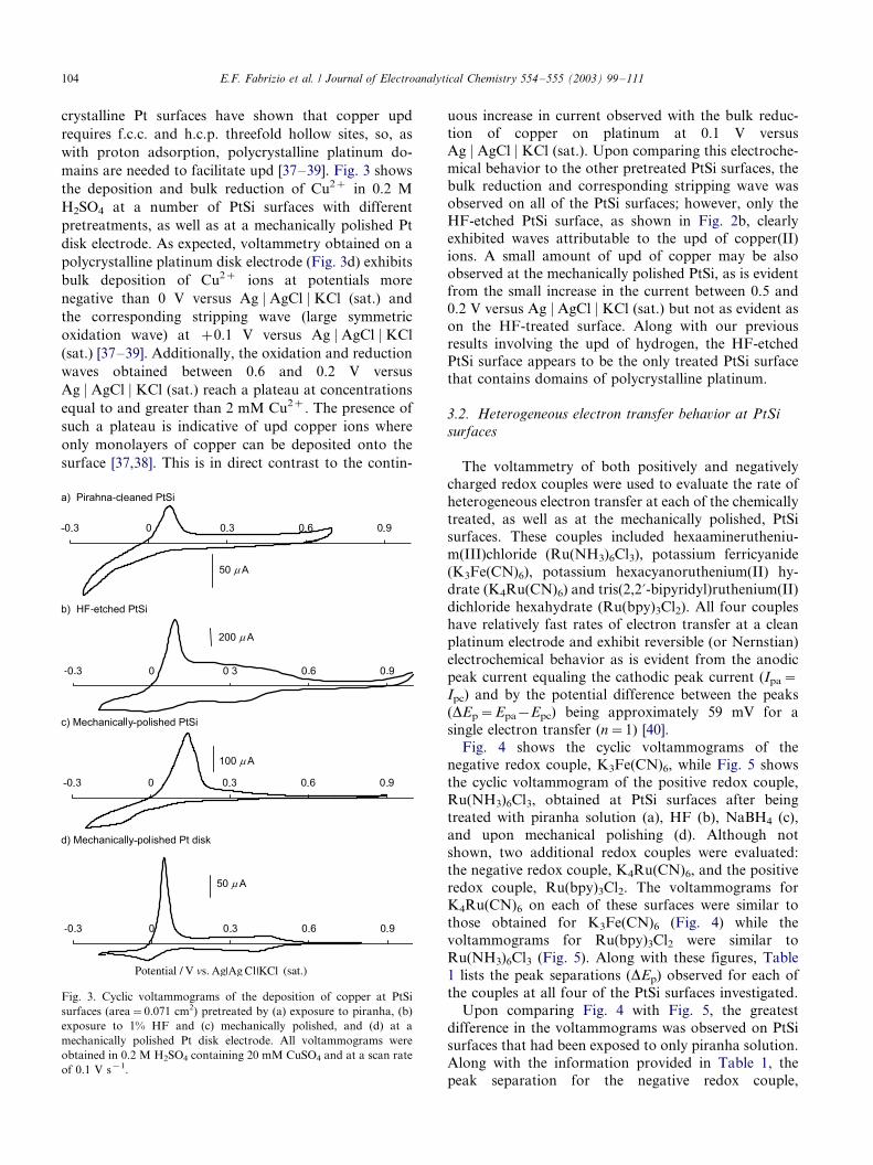
mains are needed to facilitate upd [37�/39]. Fig. 3 shows
the deposition and bulk reduction of Cu2� in 0.2 M
H2SO4 at a number of PtSi surfaces with different
pretreatments, as well as at a mechanically polished Pt
disk electrode. As expected, voltammetry obtained on a
polycrystalline platinum disk electrode (Fig. 3d) exhibits
bulk deposition of Cu2� ions at potentials more
negative than 0 V versus Ag j AgCl j KCl (sat.) and
the corresponding stripping wave (large symmetric
oxidation wave) at �/0.1 V versus Ag j AgCl j KCl
(sat.) [37�/39]. Additionally, the oxidation and reduction
waves obtained between 0.6 and 0.2 V versus
Ag j AgCl j KCl (sat.) reach a plateau at concentrations
equal to and greater than 2 mM Cu2�. The presence of
such a plateau is indicative of upd copper ions where
only monolayers of copper can be deposited onto the
surface [37,38]. This is in direct contrast to the contin-
uous increase in current observed with the bulk reduc-
tion of copper on platinum at 0.1 V versus
Ag j AgCl j KCl (sat.). Upon comparing this electroche-
mical behavior to the other pretreated PtSi surfaces, thebulk reduction and corresponding stripping wave was
observed on all of the PtSi surfaces; however, only the
HF-etched PtSi surface, as shown in Fig. 2b, clearly
exhibited waves attributable to the upd of copper(II)
ions. A small amount of upd of copper may be also
observed at the mechanically polished PtSi, as is evident
from the small increase in the current between 0.5 and
0.2 V versus Ag j AgCl j KCl (sat.) but not as evident ason the HF-treated surface. Along with our previous
results involving the upd of hydrogen, the HF-etched
PtSi surface appears to be the only treated PtSi surface
that contains domains of polycrystalline platinum.
3.2. Heterogeneous electron transfer behavior at PtSi
surfaces
The voltammetry of both positively and negativelycharged redox couples were used to evaluate the rate of
heterogeneous electron transfer at each of the chemically
treated, as well as at the mechanically polished, PtSi
surfaces. These couples included hexaaminerutheniu-
m(III)chloride (Ru(NH3)6Cl3), potassium ferricyanide
(K3Fe(CN)6), potassium hexacyanoruthenium(II) hy-
drate (K4Ru(CN)6) and tris(2,2?-bipyridyl)ruthenium(II)
dichloride hexahydrate (Ru(bpy)3Cl2). All four coupleshave relatively fast rates of electron transfer at a clean
platinum electrode and exhibit reversible (or Nernstian)
electrochemical behavior as is evident from the anodic
peak current equaling the cathodic peak current (Ipa�/
Ipc) and by the potential difference between the peaks
(DEp�/Epa�/Epc) being approximately 59 mV for a
single electron transfer (n�/1) [40].
Fig. 4 shows the cyclic voltammograms of thenegative redox couple, K3Fe(CN)6, while Fig. 5 shows
the cyclic voltammogram of the positive redox couple,
Ru(NH3)6Cl3, obtained at PtSi surfaces after being
treated with piranha solution (a), HF (b), NaBH4 (c),
and upon mechanical polishing (d). Although not
shown, two additional redox couples were evaluated:
the negative redox couple, K4Ru(CN)6, and the positive
redox couple, Ru(bpy)3Cl2. The voltammograms forK4Ru(CN)6 on each of these surfaces were similar to
those obtained for K3Fe(CN)6 (Fig. 4) while the
voltammograms for Ru(bpy)3Cl2 were similar to
Ru(NH3)6Cl3 (Fig. 5). Along with these figures, Table
1 lists the peak separations (DEp) observed for each of
the couples at all four of the PtSi surfaces investigated.
Upon comparing Fig. 4 with Fig. 5, the greatest
difference in the voltammograms was observed on PtSisurfaces that had been exposed to only piranha solution.
Along with the information provided in Table 1, the
peak separation for the negative redox couple,
Fig. 3. Cyclic voltammograms of the deposition of copper at PtSi
surfaces (area�/0.071 cm2) pretreated by (a) exposure to piranha, (b)
exposure to 1% HF and (c) mechanically polished, and (d) at a
mechanically polished Pt disk electrode. All voltammograms were
obtained in 0.2 M H2SO4 containing 20 mM CuSO4 and at a scan rate
of 0.1 V s�1.
E.F. Fabrizio et al. / Journal of Electroanalytical Chemistry 554�/555 (2003) 99�/111104

K3Fe(CN)6, is considerably larger than the peak separa-
tion observed for the positive redox couple,
Ru(NH3)6Cl3. Additionally, while the anodic peak
current was equal to the cathodic peak currents for
positive redox couples, this was not the case for the
negative redox couples. The large peak separation forthe negative redox couples suggests a considerably
slower rate of heterogeneous electron for these couples
when compared with the positive redox couples. In
direct contrast, the only PtSi surface that came close to
exhibiting Nernstian behavior with peak separations
approaching 59 mV was the mechanically polished
surface, which had peak separations ranging from
approximately 70 to 110 mV. Finally, as shown inFigs. 2�/5, the voltammetric peak currents increased
upon the removal of the oxide layer either by exposure
of the PtSi surface to the etchant, HF or by mechani-
cally polishing the surface. Such an increase in current
suggests an increase in the electrochemically active
surface area upon removal of this oxide layer.
Based on the above voltammetric results, the sluggish
electron transfer of the negative redox couples appearsto be directly associated with the amount of the oxide
layer on the PtSi surface, with the surface exposed to
piranha solution, a strong oxidant, having the slowest
rate. One possible explanation for this behavior is that a
Frumkin or potential field effect exists due to the
presence of the negative oxide layer at the electrode
surface. This layer can potentially interfere with the
ability of the negative redox couple to approach thesurface requiring a greater driving voltage to facilitate
electron transfer [40]. Similar behavior has been ob-
served at glassy carbon electrodes modified with 4-
aminobenzoic acid where the presence of surface car-
boxylates significantly decreased the rate of electron
transfer of K3Fe(CN)6 [41]. High concentrations of ions
in the electrolyte solution, however, should minimize
this effect. Another plausible reason for this effect is thatthe electrode surface is being blocked by a species that
forms an insoluble film during oxidation and reduction.
Previous studies involving the electrochemistry and
spectroscopy of Fe(CN)63�/4� have confirmed precipita-
tion of an insoluble material onto the electrode surface
upon the oxidation of Fe(CN)64� [42�/45]. This precipi-
tate, which is dependent upon the cation present in the
electrolyte as well as the electrode size, has been shownto slowdown the rate of electron transfer. One contra-
diction to this explanation, however, is that similar
behavior was also observed for Ru(CN)63�/4� which, so
far, has not been shown to form an insoluble film upon
reduction.
In an attempt to clarify the reason for the sluggish
electron transfer of negative redox couples at the
piranha-exposed PtSi, the oxidation of ferrocene dicar-boxylate, where the charge on the redox couple goes
from �/2 to �/1, and the reduction of potassium
hexachloroiridiate (K2IrCl6), where the redox couple
charge goes from a �/2 to a �/3, was also investigated at
Fig. 4. Cyclic voltammograms of 10 mM K3Fe(CN)6 in 0.1 M KCl at
PtSi surfaces (area�/0.071 cm2) pretreated by (a) exposure to piranha,
(b) exposure to 1% HF, and (c) exposure to 1.0 M NaBH4. Cyclic
voltammogram of 4.4 mM K3Fe(CN)6 at (d) a mechanically polished
PtSi surface (area�/0.031 cm2) at a scan rate of 0.1 V s�1.
Fig. 5. Cyclic voltammograms of 10 mM Ru (NH3)6Cl3 in 0.1 M KCl
at PtSi surfaces (area�/0.071 cm2) pretreated by (a) exposure to
piranha, (b) exposure to 1% HF, and (c) exposure to 1.0 M NaBH4.
Cyclic voltammogram of 3.3 mM Ru(NH3)6Cl3 obtained at (d) a
mechanically polished PtSi surface (area�/0.031 cm2) and at a scan
rate of 0.1 V s�1.
E.F. Fabrizio et al. / Journal of Electroanalytical Chemistry 554�/555 (2003) 99�/111 105
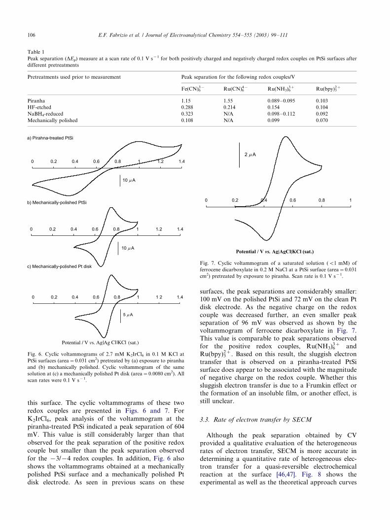
this surface. The cyclic voltammograms of these two
redox couples are presented in Figs. 6 and 7. For
K2IrCl6, peak analysis of the voltammogram at the
piranha-treated PtSi indicated a peak separation of 604
mV. This value is still considerably larger than that
observed for the peak separation of the positive redox
couple but smaller than the peak separation observed
for the �/3/�/4 redox couples. In addition, Fig. 6 also
shows the voltammograms obtained at a mechanically
polished PtSi surface and a mechanically polished Pt
disk electrode. As seen in previous scans on these
surfaces, the peak separations are considerably smaller:
100 mV on the polished PtSi and 72 mV on the clean Pt
disk electrode. As the negative charge on the redox
couple was decreased further, an even smaller peak
separation of 96 mV was observed as shown by the
voltammogram of ferrocene dicarboxylate in Fig. 7.This value is comparable to peak separations observed
for the positive redox couples, Ru(NH3)63� and
Ru(bpy)32�. Based on this result, the sluggish electron
transfer that is observed on a piranha-treated PtSi
surface does appear to be associated with the magnitude
of negative charge on the redox couple. Whether this
sluggish electron transfer is due to a Frumkin effect or
the formation of an insoluble film, or another effect, isstill unclear.
3.3. Rate of electron transfer by SECM
Although the peak separation obtained by CV
provided a qualitative evaluation of the heterogeneous
rates of electron transfer, SECM is more accurate in
determining a quantitative rate of heterogeneous elec-tron transfer for a quasi-reversible electrochemical
reaction at the surface [46,47]. Fig. 8 shows the
experimental as well as the theoretical approach curves
Table 1
Peak separation (DEp) measure at a scan rate of 0.1 V s�1 for both positively charged and negatively charged redox couples on PtSi surfaces after
different pretreatments
Pretreatments used prior to measurement Peak separation for the following redox couples/V
Fe(CN)63� Ru(CN)6
4� Ru(NH3)63� Ru(bpy)3
2�
Piranha 1.15 1.55 0.089�/0.095 0.103
HF-etched 0.288 0.214 0.154 0.104
NaBH4-reduced 0.323 N/A 0.098�/0.112 0.092
Mechanically polished 0.108 N/A 0.099 0.070
Fig. 6. Cyclic voltammograms of 2.7 mM K2IrCl6 in 0.1 M KCl at
PtSi surfaces (area�/0.031 cm2) pretreated by (a) exposure to piranha
and (b) mechanically polished. Cyclic voltammogram of the same
solution at (c) a mechanically polished Pt disk (area�/0.0080 cm2). All
scan rates were 0.1 V s�1.
Fig. 7. Cyclic voltammogram of a saturated solution (B/l mM) of
ferrocene dicarboxylate in 0.2 M NaCl at a PtSi surface (area�/0.031
cm2) pretreated by exposure to piranha. Scan rate is 0.1 V s�1.
E.F. Fabrizio et al. / Journal of Electroanalytical Chemistry 554�/555 (2003) 99�/111106
for Ru(NH3)63� at a PtSi surface that was exposed to
piranha solution prior to the SECM measurement. In
this case, the tip potential was held at �/0.28 V versus
Ag j AgCl j KCl (sat.) while the substrate was biased at
a potential of 0.1 V versus Ag j AgCl j KCl (sat.)
corresponding to an overpotential of 0.260 V. As Fig.
8 shows, the experimental curves agree well with the
diffusion-controlled theoretical fit indicating a fast rate
of electron transfer for Ru(NH3)63� at this surface. Even
as the potential approached E8 (�/0.16 V versus
Ag j AgCl j KCl (sat.)), diffusion-controlled positive
feedback was still observed. This was not the case for
Fe(CN)63�. Fig. 9a shows the experimental as well as the
theoretical approach curves for this redox couple at the
same PtSi surface. The most noticeable difference is that
negative feedback is now observed at a potential of 0.8 V
versus Ag j AgCl j KCl (sat.), which corresponds to an
overpotential of 0.58 V. Even at a potential of 1.1 V
versus Ag j AgCl j KCl (sat.) where positive feedback is
observed, the normalized current is considerably lower
than that observed for Ru(NH3)63�. This behavior
confirms a kinetic-controlled mechanism instead of a
diffusion-controlled mechanism. From the theoretical
fits given in Fig. 9a, the potential-dependent rate
constant, kf, was determined for each substrate potential
and the natural log of this rate constant plotted as afunction of the substrate potential. This plot is given in
Fig. 9b. A linear response was observed with a slope of
10.97 V�1 and an intercept of �/14.7 at the E8 of 0.180
V versus Ag j AgCl j KCl (sat.). From the Butler�/
Volmer relation, a transfer coefficient (a ) of 0.28 and
a standard rate constant (k8) of 2.9�/10�6 cm s�1 were
determined. This is considerably slower than the stan-
dard rate constant of 0.1 cm s�1 reported at cleanplatinum electrodes [42]. Overall, the quantitative rate of
electron transfer as determined by SECM agrees well
with that estimated from the peak separation observed
in the CV. Based on these results, the electron transfer
rate of the positive redox couples appears to be
considerably faster than the more negatively charged
redox couples on this surface.
3.4. Surface analysis of piranha-treated PtSi surfaces
As the above results indicate, the sluggish rate of
electron transfer of the negative redox couples appears
to be associated with an oxide layer on the PtSi. To
Fig. 8. SECM approach curve for 1 mM Ru(NH3)6Cl3 in 0.2 M NaCl
with the tip potential biased on �/0.28 V vs. Ag j AgCl j KCl (sat.) and
the substrate potential biased at 0.1 V vs. Ag j AgCl. Approach rate
was 3 mm s�1.Fig. 9. (a) SECM approach curves for 1 mM K3Fe(CN)6 in 0.1 M
NACl with the tip potential set at 0 V vs. Ag j AgCl j KCl (sat.) and
the substrate set at 1.1 V (a), 1.0 V (b), 0.95 V (c), 0.9 V (d), 0.85 V (e),
and 0.8 V (f) vs. Ag j AgCl j KCl (sat.). Approach rate was 3 mm s�1.
(b) Plot of the natural log of the potential-dependent rate constant (kf)
as a function of substrate potential.
E.F. Fabrizio et al. / Journal of Electroanalytical Chemistry 554�/555 (2003) 99�/111 107

confirm the presence of silicon oxide, which could be
used for covalent attachment of ECL labels to the
surface, a depth profile of the PtSi layer as well as the
atomic concentrations of the surface elements were
obtained using high-resolution XPS. Fig. 10 shows the
concentrations of platinum, silicon, and oxygen in atom
percentages as a function of the distance (A) probed into
a PtSi sample that was pretreated with piranha. While
the first layers contain PtSi2O4, the underlying PtSi
layers appear to show a Pt:Si 1:1 ratio down to 146 A.
These results, which show a higher percentage of silicon
on the surface and a 1:1 Pt to Si ratio below the surface,
agree with previously reported surface analyses
[16,48,49]. In addition to the depth profiling, a high-
resolution surface scan was performed after different
pretreatments to evaluate the atomic concentrations of
Pt, Si and O on each of these PtSi surfaces. These
concentrations were determined by integrating the peak
area for Pt 4f at a binding energy of 68�/88 eV, Si 2p at a
binding energy of 145�/165 eV and O 1s at a binding
energy of 525�/545 eV and are given in Table 2. The HF-
etched surface, which showed a mole ratio for the three
components of Pt4SiO2, had the highest amount of Pt on
the surface, while the mechanically polished surface,
which showed a mole ratio of PtSiO2, was the only
surface that exhibited a 1:1 Pt to Si ratio. The piranha-
and borohydride-treated surfaces showed almost the
same composition and agree with the atomic concentra-
tions measured on the surface of different samples
analyzed during the depth profiling. Based on the
electrochemical results, one would expect the NaBH4-treated surface to have less oxygen than the piranha-
treated surface. However, these samples were exposed to
air prior to the XPS measurement and so the NaBH4-
treated surface may have undergone further oxidization
before analysis. This may also be the case for the
mechanically polished PtSi, which also contained an
unexpectedly high amount of surface oxide.
3.5. Topography and localized conductivity by AFM
As the above studies show, the presence of an oxide
layer on the PtSi surface still allows the transfer
electrons although at a higher overpotential. One
question that remains is whether electron transfer occurs
across the whole surface through tunneling or only atlocalized domains. Although SECM can be used to map
areas of electron transfer at interfaces, the resolution
with the tip used to obtain the approach curves was not
high enough to determine whether there were localized
regions of electron transfer on this surface. An alter-
native was to use AFM modified with a conductive tip
to measure the variation in film conductivity over sub-
micron length scales by monitoring the current flowfrom the conductive tip to the PtSi film during an
applied d.c. bias. Fig. 11 shows the surface topography
(a) and conductivity (b) images obtained for a PtSi film
exposed to piranha. In agreement with previous studies,
the AFM topography (Fig. 11a) shows that the PtSi
coating is fairly smooth (�/1.3 nm root mean-square
(RMS) surface roughness) but non-uniformly distribu-
ted. The presence of small pinhole-like topographicdefects, approximately 20 nm in diameter, are observed
between the larger PtSi grains. Comparison of the
simultaneously acquired topography (Fig. 11a) and
Fig. 10. Depth profile showing the atomic concentrations of Pt, Si and
O as a function of depth probed (A) on PtSi after exposure to piranha.
Table 2
Atomic concentrations on the surface of different pretreated PtSi by
high-resolution XPS
Chemical pretreat-
ments
Atomic concentration/%
Pt1 (68�/
88 eV)
Si2 (145�/
165 eV)
O1 (525�/
545 eV)
Piranha 15 27 58
NaBH4 16 25 59
HF-etched 54 14 32
Mechanically po-
lished
29 25 46
Binding energies (eV) used for the analysis are provided in
parentheses after the atom.
E.F. Fabrizio et al. / Journal of Electroanalytical Chemistry 554�/555 (2003) 99�/111108
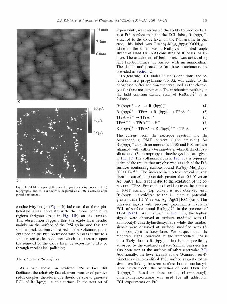
conductivity image (Fig. 11b) indicates that these pin-hole-like areas correlate with the more conductive
regions (brighter areas in Fig. 11b) on the surface.
This observation suggests that the oxide layer resides
mainly on the surface of the PtSi grains and that the
smaller peak currents observed in the voltammograms
obtained on the PtSi pretreated with piranha is due to a
smaller active electrode area which can increase upon
the removal of the oxide layer by exposure to HF orthrough mechanical polishing.
3.6. ECL on PtSi surfaces
As shown above, an oxidized PtSi surface stillfacilitates the relatively fast electron transfer of positive
redox couples; therefore, one should be able to generate
ECL of Ru(bpy)32� at this surface. In the next set of
experiments, we investigated the ability to produce ECL
at a PtSi surface that has the ECL label, Ru(bpy)32�,
attached to the oxide layer on the PtSi grains. In one
case, this label was Ru(bpy-Me2)2(bpy-(COOH)2)2�
while in the other was a Ru(bpy)32� labeled single
strand of DNA (ssDNA) consisting of 10 bases (or 10-
mer). The attachment of both species was achieved by
first functionalizing the surface with an aminosilane.
The details and procedure for these attachments are
provided in Section 2.
To generate ECL under aqueous conditions, the co-
reactant, tri-n -propylamine (TPrA), was added to thephosphate buffer solution that was used as the electro-
lyte for these measurements. The mechanism resulting in
the light emitting excited state of Ru(bpy)32� is as
follows:
Ru(bpy)2�3 �e� 0 Ru(bpy)3�
3 (4)
Ru(bpy)3�3 �TPrA 0 Ru(bpy)2�
3 �TPrA�+ (5)
TPrA�e� 0 TPrA�+ (6)
TPrA�+ 0 TPrA�+�H� (7)
Ru(bpy)3�3 �TPrA+ 0 Ru(bpy)2�
3 ��TPrA (8)
The current from the electrode reaction and the
corresponding PMT current (light emission) for
Ru(bpy)32� at both an unmodified PtSi and PtSi surfaces
silanized with either (4-aminobutyl)-dimethylmethoxy-
silane and (3-aminopropyl)-trimethoxysilane are given
in Fig. 12. The voltammogram in Fig. 12a is represen-tative of the results that are observed at each of the PtSi
surfaces containing surface bound Ru(bpy-Me2)2(bpy-
(COOH)2)2�. The increase in electrochemical current
(bottom curve) at potentials greater than 0.8 V versus
Ag j AgCl j KCl (sat.) is due to the oxidation of the co-
reactant, TPrA. Emission, as is evident from the increase
in PMT current (top curve), is not observed until
Ru(bpy)32� is oxidized to the 3�/ state at potentials
greater than 1.2 V versus Ag j AgCl j KCl (sat.). This
behavior agrees with previous experiments involving
ECL of surface bound Ru(bpy)32� in the presence of
TPrA [50,51]. As is shown in Fig. 12b, the highest
signals were observed at surfaces modified with (4-
aminobutyl)-dimethylmethoxysilane while the smallest
signals were observed at surfaces modified with (3-
aminopropyl)-trimethoxysilane. We suspect that themoderate signal observed at the unmodified PtSi is
most likely due to Ru(bpy)32� that is non-specifically
adsorbed to the oxidized surface. Similar behavior has
also been seen at the surfaces of other electrodes [50].
Additionally, the lower signals at the (3-aminopropyl)-
trimethoxysilane-modified PtSi surface suggests exten-
sive cross-linking between surface bound methoxysi-
lanes which blocks the oxidation of both TPrA andRu(bpy)3
2�. Based on these results, (4-aminobutyl)-
dimethylmethoxysilane was used for all additional
ECL experiments on PtSi.
Fig. 11. AFM images (1.0 mm�/1.0 mm) showing measured (a)
topography and (b) conductivity acquired at a PtSi electrode after
piranha treatment.
E.F. Fabrizio et al. / Journal of Electroanalytical Chemistry 554�/555 (2003) 99�/111 109
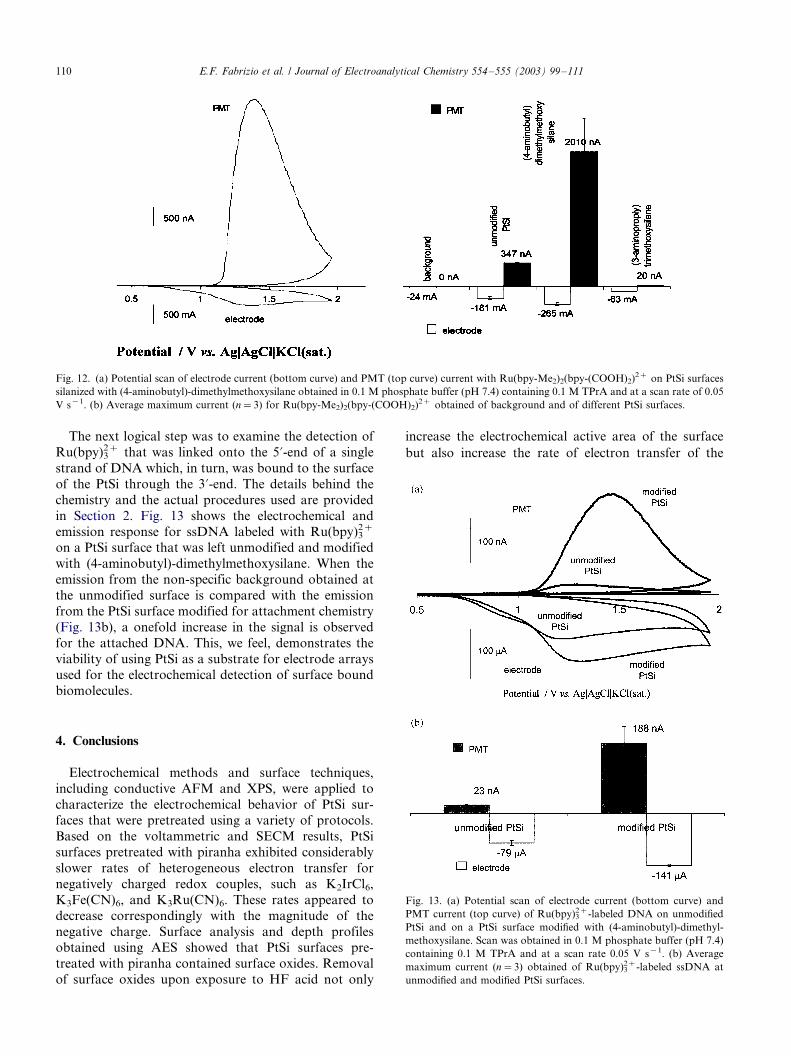
The next logical step was to examine the detection of
Ru(bpy)32� that was linked onto the 5?-end of a single
strand of DNA which, in turn, was bound to the surface
of the PtSi through the 3?-end. The details behind the
chemistry and the actual procedures used are provided
in Section 2. Fig. 13 shows the electrochemical and
emission response for ssDNA labeled with Ru(bpy)32�
on a PtSi surface that was left unmodified and modified
with (4-aminobutyl)-dimethylmethoxysilane. When the
emission from the non-specific background obtained at
the unmodified surface is compared with the emission
from the PtSi surface modified for attachment chemistry
(Fig. 13b), a onefold increase in the signal is observed
for the attached DNA. This, we feel, demonstrates the
viability of using PtSi as a substrate for electrode arraysused for the electrochemical detection of surface bound
biomolecules.
4. Conclusions
Electrochemical methods and surface techniques,
including conductive AFM and XPS, were applied to
characterize the electrochemical behavior of PtSi sur-faces that were pretreated using a variety of protocols.
Based on the voltammetric and SECM results, PtSi
surfaces pretreated with piranha exhibited considerably
slower rates of heterogeneous electron transfer for
negatively charged redox couples, such as K2IrCl6,
K3Fe(CN)6, and K3Ru(CN)6. These rates appeared to
decrease correspondingly with the magnitude of the
negative charge. Surface analysis and depth profilesobtained using AES showed that PtSi surfaces pre-
treated with piranha contained surface oxides. Removal
of surface oxides upon exposure to HF acid not only
increase the electrochemical active area of the surface
but also increase the rate of electron transfer of the
Fig. 12. (a) Potential scan of electrode current (bottom curve) and PMT (top curve) current with Ru(bpy-Me2)2(bpy-(COOH)2)2� on PtSi surfaces
silanized with (4-aminobutyl)-dimethylmethoxysilane obtained in 0.1 M phosphate buffer (pH 7.4) containing 0.1 M TPrA and at a scan rate of 0.05
V s�1. (b) Average maximum current (n�/3) for Ru(bpy-Me2)2(bpy-(COOH)2)2� obtained of background and of different PtSi surfaces.
Fig. 13. (a) Potential scan of electrode current (bottom curve) and
PMT current (top curve) of Ru(bpy)32�-labeled DNA on unmodified
PtSi and on a PtSi surface modified with (4-aminobutyl)-dimethyl-
methoxysilane. Scan was obtained in 0.1 M phosphate buffer (pH 7.4)
containing 0.1 M TPrA and at a scan rate 0.05 V s�1. (b) Average
maximum current (n�/3) obtained of Ru(bpy)32�-labeled ssDNA at
unmodified and modified PtSi surfaces.
E.F. Fabrizio et al. / Journal of Electroanalytical Chemistry 554�/555 (2003) 99�/111110
negative redox couples. Furthermore, the upd of both
protons and copper(II) ions also confirmed the presence
of polycrystalline platinum domains on the surface of
the PtSi after exposure to HF. AFM with a conductivetip to study the topography along with the localized
surface conductivity showed that, in the presence of this
oxide layer, electron transfer occurs at nanoscale
domains located between PtSi grains. As a result of
these properties, we were able to generated ECL from
Ru(bpy)32� bound to the oxidized PtSi surface demon-
strating the feasibility of using this surface as a platform
for chemical and biological assays that use electroche-mical detection.
Acknowledgements
Support from the National Science Foundation
(CHE9876855) is greatly appreciated.
References
[1] M.P. Lepselter, S.M. Sze, Bell Syst. Tech. J. 47 (1968) 195.
[2] M.P. Lepselter, J.M. Andrews, in: B. Schwartz (Ed.), The
Electrochemical Society Softbound Symposium Series, New
York, 1969, p. 159.
[3] A.H. Huchberg, Transactions: Electronic Materials Processing
Conference, Materials Research Corp, Orangeburg, NY, 1973, p.
81.
[4] S.P. Murarka, J. Vac. Sci. Technol. 17 (1980) 775.
[5] E.H. Roderick, R.H. Williams, Metal Semiconductor Contacts,
Clarendon Press, Oxford, 1988, p. 201.
[6] A. Czernik, H. Palm, W. Cabanski, M. Shultz, V. Suckow, Appl.
Phys. A 55 (1992) 180.
[7] A.K. Vijh, G. Belanger, R. Jacques, Int. J. Hydrogen Energy 15
(1990) 789.
[8] A.K. Vijh, G. Belanger, R. Jacques, Int. J. Hydrogen Energy 17
(1992) 479.
[9] A.K. Vijh, G. Berlanger, R. Jacques, J. Mater. Sci. Lett. 12 (1993)
113.
[10] F.-R.F. Fan, G.A. Hope, A.J. Bard, J. Electrochem. Soc. 129
(1982) 1647.
[11] F.-R.F. Fan, R.G. Keil, A.J. Bard, J. Am. Chem. Soc. 105 (1983)
220.
[12] H. Morisaki, H. Ono, K. Yazawa, J. Electrochem. Soc. 135 (1998)
381.
[13] H. Morisaki, H. Ono, K. Yazawa, Proc. Electrochem. Soc.
(Photoelectrochem. Electrosynthesis Semiconductor Mater.) 88
(1988) 436.
[14] H. Morisaki, H. Ono, K. Yazawa, J. Electrochem. Soc. 136 (1989)
1710.
[15] C.-A. Chang, J. Appl. Phys. 59 (1986) 3116.
[16] C.A. Dimitriadis, E.K. Polychroniadis, E.K. Evangelou, G.E.
Giakoumakis, J. Appl. Phys. 70 (1991) 3019.
[17] S.R. Das, D.-X. Xu, J. Phillips, J. McCaffrey, L. LeBrun, A.
Naem, in: S.P. Murarka, K. Rose, T. Ohmi, T. Seidel (Eds.),
Mater. Res. Soc. Symp. Proc., Vol. 318, Materials Research
Society, Pittsburgh, PA, 1994, p. 129.
[18] K. Maex, M. Van Rossum, A. Reader, in: K. Maex, M. Van
Rossum (Eds.), EMIS Trans Data Review Series, 1995, p. 14.
[19] U. Diebold, L. Zhang, J.F. Anderson, P. Mrozek, J. Vac. Sci.
Technol. A 14 (1996) 1679.
[20] E.P. Domashevskaya, Y.A. Yurakov, V.M. Kashkarov, Thin
Solid Films 298 (1997) 135.
[21] S.J. Naftel, I. Coulthard, T.K. Sham, D.-X. Xu, L. Erickson, S.R.
Das, Thin Solid Films 58 (1997) 308.
[22] A. Rahman, C.W. Bates, Jr., A.F. Marshall, S.B. Qadri, T. Bari,
Mater. Lett. 39 (1999) 343.
[23] D.M. Solina, R.W. Cheary, P.D. Swift, S. Dligatch, G.M.
McCredie, B. Gong, P. Lynch, Thin Solid Films 372 (2000) 94.
[24] C. Detavernier, R. De Gryse, R.L. Van Meirhaeghe, F. Cardon,
G.-P. Ru, X.-P. Qu, B.-Z. Li, R.A. Donaton, K. Maex, J. Vac.
Sci. Technol. A 18 (2000) 470.
[25] J. Shi, D. Kojima, M. Hashimoto, J. Appl. Phys. 88 (2000) 1679.
[26] G.A. Hope, F.-R.F. Fan, A.J. Bard, J. Electrochem. Soc. 130
(1983) 1488.
[27] F.F. Fan, D. Cliffel, A.J. Bard, Anal. Chem. 70 (1998) 2941.
[28] Y. Zu, Z. Ding, J. Zhou, Y. Lee, A.J. Bard, Anal. Chem. 73 (2001)
2153.
[29] G. Sprintschnik, H. Sprintschnik, P.P. Kirsch, D.G. Whitten, J.
Am. Chem. Soc. 99 (1977) 4947.
[30] A. Juris, V. Balzani, F. Barigelletti, S. Campagna, P. Belser, A.
Von Zelewsky, Coord. Chem. Rev. 84 (1988) 85.
[31] F. Pichet, J.H. Beck, C.M. Elliot, J. Phys. Chem. A 103 (1999)
6263.
[32] C.M. Elliot, E.S. Hershenhart, J. Am. Chem. Soc. 104 (1982)
7519.
[33] J.O’M. Bockris, A.K.N. Reddy, Modern Electrochemistry, Vol. 2,
Plenum Press, New York, 1970, pp. 1153�/1156, 1223�/1251.
[34] B.E. Conway, L. Bai, J. Electroanal. Chem. 198 (1986) 149.
[35] E.J. Yeager, J. Electrochem. Soc. 128 (1981) 160C.
[36] B.E. Conway, in: A. Wieckowski (Ed.), Interfacial Electrochem-
istry: Theory, Experimental and Applications, Marcel Dekker,
New York, 1999, pp. 135�/148.
[37] R. Gomez, H.S. Yee, G.M. Bommarito, J.M. Feliu, H.D.
Abruna, Surf. Sci. 335 (1995) 101.
[38] C.A. Lucas, N.M. Markovic, P.N. Ross, Phys. Rev. B 56 (1997)
3651.
[39] E. Herrero, S. Glazier, L.J. Buller, H.D. Abruna, J. Electroanal.
Chem. 461 (1999) 121.
[40] A.J. Bard, L.R. Faulkner, Electrochemical Methods: Fundamen-
tals and Applications, 2nd ed., Wiley, New York, 2000, pp. 239�/
241.
[41] J. Ye, J. Liu, Z. Zhang, J. Hu, S. Dong, Y. Shoa, J. Electroanal.
Chem. 508 (2001) 123.
[42] C. Beriet, D. Pletcher, Electroanal. Chem. 361 (1993) 93.
[43] K. Winkler, J. Electroanal. Chem. 388 (1995) 151.
[44] C.M. Pharr, P.R. Griffiths, Anal. Chem. 69 (1997) 4665.
[45] C.M. Pharr, P.R. Griffiths, Anal. Chem. 69 (1997) 4673.
[46] D.O. Wipf, A.J. Bard, J. Electrochem. Soc. 138 (1991) 469.
[47] A.J. Bard, M.V. Mirkin, P.R. Unwin, D.O. Wipf, J. Phys. Chem.
96 (1992) 1861.
[48] T.J. Kingzett, C.A. Ladas, J. Electrochem. Soc. 122 (1975) 1729.
[49] R.J. Blattner, C.A. Evans, Jr., S.S. Lau, J.W. Mayer, B.M.
Ullrich, J. Electrochem. Soc. 122 (1975) 1732.
[50] X.-H. Xu, A.J. Bard, Langmuir 10 (1994) 2409.
[51] X.-H. Xu, A.J. Bard, J. Am. Chem. Soc. 117 (1995) 2627.
E.F. Fabrizio et al. / Journal of Electroanalytical Chemistry 554�/555 (2003) 99�/111 111