Embed Size (px)
Citation preview
'AD-ft@3 233 ELECTRO-OPTICAL CHRACTERIZATION OF THE TEKTRONIX 1/1TK5I2N-SiI CCO (CHRGE-..(U) AIRIZONA UNIY TUCSON DEPTOF CHEMISTRY P M EPPERSON ET AL. 67 JUL 87 TR-51
UMhSIFED hhEE-K-31hh 91hImhhmmhhmhmus*:uuuuuuuuuol
AL
11111L-5 1.0 -L4 11 6
MICRCOP RESOUTO TES22ARNAIOA BUEUO TNDRS16-
1111 ~, m~M12.1H11 II
S1#CURITY CLASIFICATION OF THIS PAGE OWhen Dee eneed)
REORTI DOCUMEt4TATIOtI PAGE READ INUCTION0S'~'~"'BEFORE COMPLETING FoRd
1.REOR NM6ER GOVT ACCESSION NO. 3. R9CIPIENV:S CATALOG NUMBER
4. TITLE (and Subtite) S. TYPE OF REPORT & PIEF00 COVERED
Electro-Optical Characterization of the Tektronix InterimTK512M-O11 CCD _______________
6. PERFORMING ORG. REPORT NUMBER
I. AAJTNORE') . CONT-RACT OR GRANT MUM11ERIs)
Patrick M. Epperson, Jonathan V . Swee'ilerM. Bonner Denton, Gary R. Sims, Thomas W. N00014-83-K-0268McCurnin and Richard 5. Aikens _____________
S. PERFORMING ORGANIZATION NAME AND ADDRESS 10. PROGRAM ELEMENT. PROJECT. TASKC
Department of Chemistry NR 051-5~49U UBR
University of ArizonaTucson. AZ 85721
11. CONTROLLING OFFICE NAME AND ADDRESS 12. REPORT OATE
Office of Naval Research July 9,.1987Arlington, Virginia 22217 13. NUMBER OF PAGES
____ ___ ___ ___ ___ ___ ____ ___ ___ ___ ___ ___ ___48
14. MONITORING AGENCY NAME & ADORESS(If different Ina Contro*Iind Office) 15. SECURITY CLASS. (of this report)
Unclassified1s. DICLASSIFICATION/OWNGRADINGN SCHEDULE
III.* DISTRIBUTION STATEMENT (of this Report)
This document has been approved for public release and sale; itsdistribution is unlimited.
17. DISTRIBUTION STATEMENT (of the abstract entered In Block 20, it different traim RA) D T ICAUG 14 1987
Submitted to Optical Engineering for publication. Omsk
IS. Key WORDSI (CnSnu. en reoe eide of necessar and IdenifU. y wek innber)
Charge-C3UPled device, Charge transfer device
7-10 4--1Cs is described. This device, the TK512M-O11, is a frontside-illuminated CCD with a 512 by 512 format and 27 by 27 micron pixels. Electro-optical characteristics measured in this study include linearity, blooming,dark count rate, charge transfer efficiency (CTE), and quantum efficiency.The results of a detailed study of the noise characteristics of the COD out- Jput, ET are reported. The TK512M-O11 has excellent photometric linearity,high well capacity, and a low dark count rate..4Continued on other side)
DD I JA"7 1473 EDITION oF I Nov Ila Is OBSOLETE ('
SIN 0102.LP.014440tSECURITY CLASSIFICATION OF THSIS PAGE (Ohem Daea rnteed!
Very good low light level CTE is observed in the parallel shift direction'k.however CTE problems are observed in the serial direction. The quantumefficiency of the frontside-illuminated CCD over the wavelength range of 400to 1000 nm is reported and is lower than expected based on experience withother similar devices. The noise of the output FET of the CCD is equivalentto 5 to 12 electrons depending upon the FET operating conditions and systembandwidth. A very small latent image effect is noted. The conclusign ofthis evaluation is that despite the problems observed, the frontsidetilluminated
<ekti o, CCD is an excellent sensor for scientific imaging applications.
711i
p
li O "" '"
N ' ' '-f*4
OFFICE OF NAVAL RESEARCH
Contract N00014-86-K-0316
Task No. 051-549
TECHNICAL REPORT NO. 51
Electro-Optical Characterization of the Tektronix TK512M-011 CCD
by
Patrick M. Epperson, Jonathan V. Sweedler, M. Bonner Denton,Gary R. Sims, Thomas W. McCurnln and Richard S. Aikens
Prepared for publication in
Optical Engineering AcceiS orA
OliC 1A9
Department of Chemistry By.....University of Arizona Di:;t.i'b ----Tucson, Arizona 85721
July 7, 1987 L
o 'C
Reproduction in whole or in part is permitted forany purpose of the United States Government.
This document has been approved for public release
and sale; its distribution is unlimited.
'L_*L
/
ABSTRACT
The electro-optical characterization of the first in a new series
of Tektronix CCDs is described. This device, the TK512M-011, is a
frontside-illuminated CCD with a 512 by 512 format and 27 by 27 micron.
pixels. Electro-optical characteristics measured in this study
include linearity, blooming, dark count rate, charge transfer
efficiency (CTE), and quantum efficiency. The results of a detailed
study of the noise characteristics of the CCD output FET are reported.
The TK512M-011 has excellent photometric linearity, high well
capacity, and a low dark count rate. Very good low light level CTE is
observed in the parallel shift direction, however CTE problems are
observed in the serial direction. The quantum efficiency of the
frohtsidw-illuminated CCD over the wavelength range of 400 to 1000 nm
is reported and is lower than expected based on experience with other
similar devices. The noise of the output FET of the CCD is equivalent
to 5 to 12 electrons depending upon the FET operating conditions and
system bandwidth. A very small latent image effect is noted. The
conclusion of this evaluation is that despite the problems observed,
the frontside-illuminated Tektronix CCD is an excellent sensor for
scientific imaging applications.
1. INTRODUCT ION
For low light level scientific applications the charge-coupled
device (CCD) is the premier electronic detector for the visible,
ultraviolet, vacuum ultraviolet, and soft x-ray regions of the
electromagnetic spectrum (1,2,3,4). CCD performance in terms of
sensitivity, signal to noise ratio, and photometric accuracy is
capable of greatly exceeding that of all other imaging detectors.
Since their invention by Boyle and Smith of Bell Laboratories in 1970
(5,6), several organizations have been involved in improving the
performance of CCDs in the areas of spectral coverage, readout noise,
dark current, spatial resolution and charge transfer efficiency.
These efforts have resulted in a class of devices termed scientific
CCDs which are specifically designed to meet the needs of low light
level, wide dynamic range, scientific imaging applications. Some
specific areas in which needs for high resolution CCD imaging have
been expressed are optical and electron microscopy, streak tube
readout, high resolution multichannel optical spectroscopy,
astronomical observations, surveillance, and medical and industrial
radiology.
The ultimate goal of any detector for scientific imaging is to
efficiently convert the incoming photon flux into a two-dimensional
array of charge packets, hold the charge for the length of the
observation, and then accurately measure the amount of charge present
in each packet. Determining whether or not a new CCD is suitable for
use as a scientific imager is done by quantifying the important
physi'cal characteristics of a CCD which determine its ability to
2
tran duce an optical image Into an electronic one with high signal to
noise. Once the detector characteristics are known, the expected S/N
can be estimated given the photon flux, the wavelength region, the
integration time, and the noise which is present in the basic photon
signal.
This paper discusses the electro-optical evaluation of the first
in a family of CCDs manufactured by Tektronix which were designed for
use in scientific applications (7). The detector, TK512M-011, is a
512 by 512 frontside-illuminated 3 phase CCD with 27 by 27 micron
pixels. This CCD is the first in a family of devices which include
both front and backside-illuminated devices in 512 2, 10242 , and
20482 two-dimensional formats. This now family of CCDs represents not
only a sizeable improvement in spatial resolution available from a CCD
imager, but is also predicted to provide now performance levels in
terms of noise, sensitivity and dynamic range in a commercially
available detector. The evaluation of the TK512M-011 centers on
measuring the electro-optical properties of importance for scientific
i magi ng.
In the evaluation of the 512 by 512 CCD, the noise performance of
the on-chip amplifier is reported at several temperatures under a
variety of operating conditions. The dark count rate at several
temperatures, the quantum efficiency from 400 - 1000 nm, and the CTE
for both the serial and parallel registers are reported. Also
measured in this evaluation are linearity of response and blooming
characteristics.
Law%
' 3
2. EXPERIMENTAL APPARATUS EMPLOYED FOR CCD EVALUATION
2.1 Slow-scan CCD camera system
The camera system employed for these investigations consists of a
Photometrics CC180A high speed camera controller coupled to a CI181A
camera head interface and a modified CH181A cryogenic camera head.
The camera controller generates timing signals for the camera head
interface to facilitate charge propagation, pixel readout, and other
utility functions. This unit is programmed through manual input or
from a host computer. A flexible command set supports operations such
as subarray readout, charge binning, variable exposure time, charge
clearing, and system gain control. The controller also supervises the
transmission of digital intensity data to the host computer system.
The camera head interface contains the circuitry to generate CCD
clock waveforms, control CCD temperature, operate an electronic
shutter, perform a double correlated sample for pixel readout, and
digitize pixel intensity data. To control kTC noise, a dual-slope
integrator with variable integration times is used for subtraction of
correlated samples before and after charge transfer to the output
node. The integrator also provides electronic bandwidth control for
white and 1/f noise reduction. Intensity data is digitized to 14 bits
precision at 50 kHz rate.
The camera head consists of a liquid nitrogen cryostat containing
the CCD, preamplifier, voltage dividers, and clock signal
conditioners. The CCD temperature is adjustable over the range of -50
to -120C. The temperature is regulated to +/- .5 degrees C by a servo
controlled resistive heater system. Minor modifications were made to
4
the camera head to facilitate external control of the CCD output FET
drain voltage and current for these experiments.
2.2 Digital image acquisition, display, and processing system.
The system employed to acquire and analyze image data from the
camera system is a Photometrics DIPS 2000 unit. This is a highly
specialized computer hardware/software system designed to be used in
conjunction with Photometrics slow-scan CCD cameras. The DIPS system
is interfaced to the CC1BOA controller over a high speed DMA channel.
The computer hardware of the DIPS system consists of a MC68010
processor with 1 MBYTE program RAM and 4 MByte image buffer RAM. A 65
MByte winchester disk unit with a 67 MByte formatted cartridge tape
unit were used for program and image data storage. An
alphanumeric/graphics console terminal was used for control and
graphical data display functions. A video display memory unit was
used to display images on a RS170 monitor. Hard copies of displayed
images were obtained with a video hard copy unit.
Extensive image processing, analysis, and display software are
supported by the DIPS system. Typical functions include linear image
arithmetic functions, statistical analysis, and image display with
variable contrast and spatial format.
3. CCD OUTPUT FET AMPLIFIER CHARACTERIZATION AND OPTIMIZATION
A CCD can be used to detect extremely faint images of less than
100 photogenerated electrons per pixel and thus must have very low
noise readout amplification and digitization electronics. It is the
5
extremely low noise levels obtainable from CCDs which distinguish them
from other solid-state and vacuum tube imagers. The low readout noise
obtainable from a CCD is derived from its ability to transfer
photogenerated charge to a specialized low capacitance floating
diffusion which serves as the gate of the MOSFET amplifier. Readout
noise levels of less than 50 electrons are quite common in CCDs, while
especially superior imagers have noise levels of less than 10
electrons. The* TK512M-011 was designed to have a readout noise of 2
electrons (7). Because the same amplifier is present on every device
in the Tektronix CCD family, a great deal of effort was expended in
carefully measuring and optimizing the performance of the on-chip
preamplifier and the associated signal processing electronics.
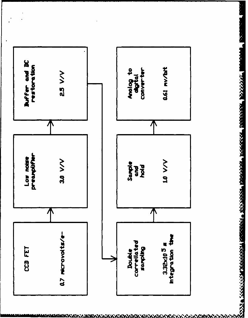
A block diagram of the signal processing scheme used to evaluate
the TK512M-011 on-chip amplifier noise characteristics is given in
Fig. 1. The potential of the output node of the CCD is amplified by
the on-chip FET amplifier. The signal from this FET amplifier is
further processed by additional gain, dc restoration circuitry and a
double correlated sampling process. Conversion to a digital format is
accomplished by a sample-hold and an analog-to-digital converter. The
optimum operating point and the noise performance of the CCD output
FET were investigated in detail.
Optimization of the CCD output FET signal-to-noise ratio required
(a) determining the voltage gain and output impedance of the device,
(b) determining the output noise from the device and then combining
(a) and (b) into an overall figure-of-merit. Given the FET output
'--
6
noise, and an output signal (assumed noiseless) the output signal-to-
noise ratio is given by:
S/N = (output signal power)/(output noise power). (1)
The following development assumes that the output noise can be
adequately represented by a flat spectral density modified by a filter
function. This assumption is justified by the low corner frequency of
the observed 1/f noise from the device, the double-correlated sample
procedure, and the high pass filtering used in the preamplifier.
Since both signal and noise appear across the same output impedance,
the output signal-to'noise ratio is
S/N - (ES *433)MEE n3*BW), (2)
where Sn is the input signal expressed in volts rms, G is the device
voltage gain from input to output, En is the device noise spectral
density expressed in volts rms across the device output impedance and
BW is the noise bandwidth of the fixed filter function in Hz.
The following decibel measure based on one volt across the output
impedance (dbv) is a monotonic function for positive arguments and is
used as a basis for a figure-of-merit:
S/Ndbv 2 0log(S n ) + 20log(G) - 20log(E n) -10log(BW).
The input signal level is arbitrary and can be kept constant for
figure of merit determination. The output filter noise bandwidth is a V
constant for a given setup of the double correlated sampling.
Therefore, the figure-of-merit (FOM) used in these studies is
FOMdbv =201og(G) - 20log(E n). (4)
7
Maximizing the above function is equivalent to maximizing the output
signal-to-noise ratio from the device for a fixed sense node
capacitance.
The output FET was characterized using a curve tracer (Fig. 2) to
determine incremental forward transconductance, gfs, using the
relationship:
s 4 1 Ids)/( AVgs (5)
Given the incremental transconductance, a source resistor Rs, and a
simple FET follower model, the gain and output impedance, Rout, of a
source follower circuit are
Gain = (gf s*Rs) /(1 + [gfs*Rs3), (6)
Rou t = R s/(1 + Cgfs*Rs]). (7)
Output noise from the *CCD output FET was measured using a
carefully calibrated spectrum analyzer. The results showed a
relatively flat spectral density plus a low-frequency 1/f region. At
good operating points the corner frequency of the 1/f region was well
below 10 kHz. The 1/f region did extend far enough to affect the
estimated noise output from the double correlated sampling at several
operating points of the FET; however, these points occurred at
relatively high overall noise values and did not represent optimum
device operating conditions.
Noise data were taken and the forward transconductance determined
at a number of operating points at +21, -80, -100, -120, and -130
degrees C. The output FET drain voltage (V ) was varied from 8 to 22
11 1 d11 1
a UWMI(
48
volts. FET source current was varied from 0.3 milliamperes to
approximately 0.8 milliamperes. The reset FET drain voltage (V ) wasg
varied from 2 to 15 volts. The FET noise was measured for over 100
different combinations of operating conditions.
The data were interpreted as follows. Using the measured FET
incremental forward transconductance values, the source follower gain
and output resistance Were computed for each operating point. Optimum
operating points as functions of temperature were then determined
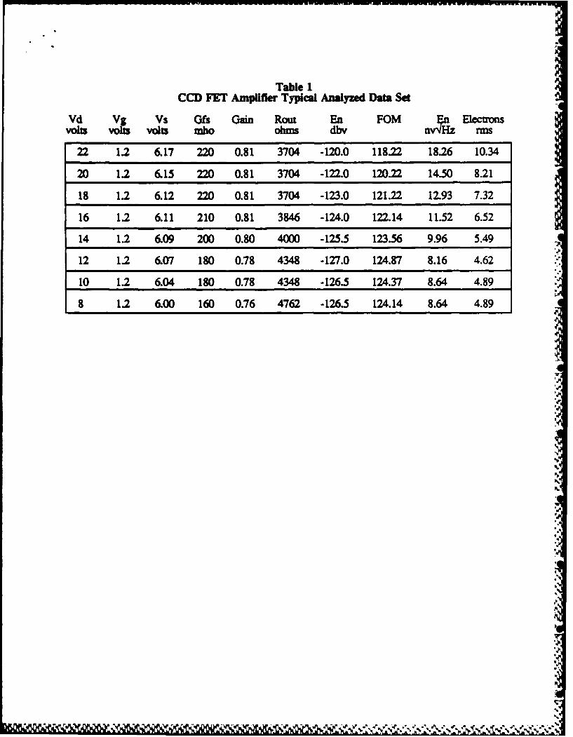
using Eq. (3). A typical analyzed data set is summarized in Table 1.
The equivalent noise in nv/j"Hz at the output FET as measured on a
spectrum analyzer in the flat portion of the spectrum is included in
Table 1. The noise was converted to equivalent electrons assuming a
CCD gain of 0.7 microvolts/electron and the full bandwidth of the
double correllated sampler.
The CCD output FET as tested supports operation at device noise
levels of approximately five electrons rms using sampling integration
times as short as 4.2 microseconds. Lower equivalent noise levels
could be realized with longer sampling integration times. We have
designed an off-chip pre-amplifier whose noise is compatible with the
noise characteristics of the device using readily available
components.
A number of good CCD FET operating points were found at all of
the cooled temperatures. In some cases at room temperature excess low
frequency noise was observed that increased with drain to source
voltage. This condition was observed at the onset of surface channel
I
9
operation of the FET at device currents exceeding 0.5 milliamperes,
and for drain to source voltages exceeding approximately 5 volts.
The total noise observed at the preamplifier output is dominated
by Johnson noise associated *with the output impedance of the CCD
output FET follower. This noise source can only be improved by
increasing the transconductance of the output FET. Finally, it must
be noted that all results reported are from measurements on a single
CCD.
4. DEVICE RESPONSE LINEARITY MEASUREMENTS
The linearity of the TK512M-011 CCD and associated analog to
digital electronics was measured. The apparatus employed for
linearity measurements consists of a ring of red light emitting diodes
(LEDs) and several light diffuser screens used to allow the LEDs to
evenly illuminate a large portion of the CCD. The flash duration of
the LEDs is computer controlled to millisecond intervals with a
reproducibility of 10 nanoseconds. In order to avoid the effects of
junction heating on the light output of the LEDs, the LEDs were
flashed for one millisecond followed by a cool down time of 20
milliseconds. The measurements were started by flashing the LEDs many
times to allow them to reach a steady temperature. The amount of
light reaching the detector was accurately and reproducibly controlled
by flashing the LEDs the desired number of times.
The linearity measurement involves using a series of uniformly
increasing exposures and plotting the observed mean signal measured in
If~ - 1 -1 ;_
10
a subarray of the CCD as a function of illumination level6. The
results are shown in Fig. 3 for exposures of zero to over 3x10⁵ e-;
this is the range of the 14 bit analog-to-digital converter with the
gain set so that the system noise is roughly equivalent to the least
significant bit. A close examination of this figure will reveal a
slight deviation from a linear response. The largest deviation from a
linear least squares line fit to the data in Fig. 3 was approximately
100 e-. These deviations divided by the response at highest5L
illumination level measured (3x10⁵ e-/detector element), give a
relative maximum deviation from a linear response of 0.03%.
5. THERMAL CHARGE GENERATION MEASUREMENTS
While the decrease in the CTE performance of the CCD at low
temperatures defines the lower temperature limit of operation, the
upper temperature limit is set by the rate of thermal generation of
charge and the longest integration time which will be used. One of
the major uses of the TK512 series of CCDs is astronomical imaging
involving long exposures; therefore, a detailed knowledge of the rate
of thermal charge generation is important. If the thermal charge
generation rate cannot be sufficiently reduced by cooling, then the
shot noise present on the thermally generated charge +or long
exposures limits the minimum detectable signal. The thermal
generation of charge, often called dark current, is due to electron-
hole pair generation by midgap defects in the bulk semiconductor and
at the Si-SiO2 interface (8). The most significant source of dark
current is from surface state defects at the Si-SiO 2 interface (9).
The thermal generation of charge was determined by taking long
integration time dark exposures and finding the mean value of a
subarray. With integration times of many minutes, cosmic ray events
and background radiation become significant and can limit the longest
integration times possible with this detector. The dark current at
142 K with a 2000 second integration time for the TK512M-011 was
measured to be 56 electrons (0.03 electrons/second), and thus
introduces less than eight electrons of noise. Fig. 4 shows the dark
counts per detector element per second observed at several
temperatures between 298 K and 140 K. Using this figure, the dark
count rate can be estimated for any desired temperature in this range.
Although the thermal charge generation rate for this CCD is low enough
for most applications, the thermal generation rate is about an order
of magnitude higher than reported for other CCD detectors (1,10).
It may be possible to reduce the dark count rate of this device
further by adjusting the parallel clock potentials. For a similar
CCD, lowering the lower parallel clock voltage during integration to
form an inversion layer under the parallel gate electrodes decreased
the dark count rate more than an order of magnitude by suppressing
thermal generation of charge from surface interface states (9). To
minimize the dark count rate as well as reduce the residual image, all
three phases should be biased to form an inversion layer, with
potential barriers between individual detector sites maintained by
irregularities in the potential wells. While reducing the dark
12
current, this also reduces the full well capacity of the individual
detector. sites and so a compromise must be made depending on the
particular application. Currently, this technique of dark count
reduction is being evaluated for the TK512M CCD.
6. SPECTRAL RESPONSE MEASUREMENTS
The sensitivity of a CCD sensor at any given wavelength is one of
the most important parameters when a particular device is being
considered for a specific scientific imaging application. For this
reason a large effort was expended to accurately measure the quantum
efficiency (charge carriers collected and measured per incident
photon) of the TK512M-011 CCD as a function of wavelength over the
near IR to ultraviolet range. These measurements were accomplished by
determining the quantity of charge generated in a subarray of the
detector during a known integration period due to photons from a
monochromatic source of known flux and wavelength.
The sensitivity of a CCD at any wavelength is strongly affected
by the optical properties of the silicon epitaxy, the overlaying gate
electrodes and the silicon dioxide layers. The sensitivity of all
CCDs decreases in the near IR due to a number of factors including the
decreasing absorption coefficient of silicon at longer wavelengths.
As the absorption coefficient decreases, photons are either absorbed
deep in the epitaxy or pass entirely through the epitaxy and are
absorbed in the bulk silicon. For devices with to micron epitaxy
layers, 90% of 1000 nm radiation passes through the epitaxy (i1).
Silicon CCDs do not respond to photons corresponding to energies less
than the band gap of silicon (approximately 1.1 &V at 300 K).
Frontside illuminated polyphase charge coupled devices constructed
with processes and structures similar to the TK512I-011 typically
exhibit very low quantum efficiencies in the blue-visible and
ultraviolet wavelengths. This is primarily due to photon absorption
and reflection from the multiple polysilicon electrodes (1,12).
The quantum efficiency measurements on the TK512M CCD are
reported for the wavelength range of 400-1000 nm. A 0.35 meter f/.8
Czerny-Turner monochromator with a 1080 line/mm grating blazed at 250
nm was used for wavelength dispersion. In order to have sufficient
throughput for flux determinations, it was necessary to open the
entrance and exit slits of the monchromator to 2.0 mm so that the
spectral bandpass was 4.0 nm. The output of the monochromator was
directed into the input port of a four inch integrating sphere which
created uniform illumination of the detector. Band pass and long
pass filters were used as necessary to prevent stray light and second
order radiation from reaching the detector. A computer controlled
electronic shutter was used to precisely control the exposure times
for the CCD. An EG&G photodiode with a calibration traceable to the
National Bureau of Standards was employed with a calibrated
picoammeter to measure the photon flux exiting the integrating
sphere/cm 2 as a function of wavelength at a precisely known distance
from the exit port. An anti-re-flection coated fused silica window
similar to the one used in the CCD camera cryostat was placed in the
U * -.,~.. * ~ ~ ;~.~.\*A- ** **** i
14
optical path between the integrating sphere and the photodiode to
compensate for reflection of this element.
To complete the quantum efficiency measurements, the photodiode
was removed from the apparatus and the CCD sensor head attached so
that the surface of the detector was at the same distance from the
exit port of the integrating sphere. The quantity of charge generated
in a subarray of the CCD during a known integration period was
determined at the same wavelengths that flux measurements were made.
The mean signal was computed and multiplied by the system gain to
determine the number of photoelectrons collected. By normalizing the
photoactive areas of both detectors and correcting for the quantum
efficiency of the photodiode, the quantum efficiency of the CCD as a
function of wavelength was calculated. The quantum efficiency
measurements on the frontside CCDs were repeated three times using one
device to test precision. A second device was tested to verify
uniformity between devices. The accuracy of the QE apparatus was
further confirmed by measuring the quantum efficiency of CCDs from RCA
and Texas Instruments and comparing the results with literature
values.
The results of the quantum efficiency measurements for the
TK512M-011 CCD are shown in Fig. 5. The quantum efficiency of the
frontside Tektronix CCD is fairly low when compared to other
multiphase frontside-illuminated CCDs such as the Thomson TH7861 (13).
The peak quantum efficiency for the devices tested occurs at 35% at
750 nm. The value drops to 3% at 400 nm and 1% at 1000 nm. The sharp
variations in sensitivity are typical of the interference effects of
L M M , 114,11 1 ' III111 11- 4 '
the gate electrodes seen in frontaide-illuminated CCDs when
illuminated with narrow band light.
While the measured quantum efficiency of the frontside imager is
lower than the literature suggests (7), the device %till has a
significant response in the 450 to 900 flu spectral range. It should
be noted that in the quantum efficiency measurements described for the
frontuide imager, the CCU was maintained at low temperature%. The
quantum efficiency of the CCD in the near IR can be increased by
operating the device athigher temperatures. .While the increase is
expected to be only a few percent at 8O0ne, it is likely the quantum'
efficiency at 1000 no can be increased several fold (14).
7. CHARGE TRANSFER EFFICIENCY MEASUREPIENTI
Charge transfer efficiency CCTE) of the CCD was measured at low
charge levels by the method of illuminating the CCD with low energy x-
rays from an Fe 55radioactive source developed by Janesick at al (1). .
CTE is generally dependent upon parallel and serial clock Levels, the
temperature of the CCD, and the amount of charge being transferred.
The most serious limitation to achieving high CTE in low light imagos
is the loss of charge to what is termed the "spurious potential
pocket" (15,1). The amount of charge trapped is a small fraction of
full well, therefore smearing is apparent only at very low light
levels.I
Because of the large number of transfers in a 5121 by 512, 7-phase W
CCD, CTE values near unity are necessary to avoid any significant
7*1W
16
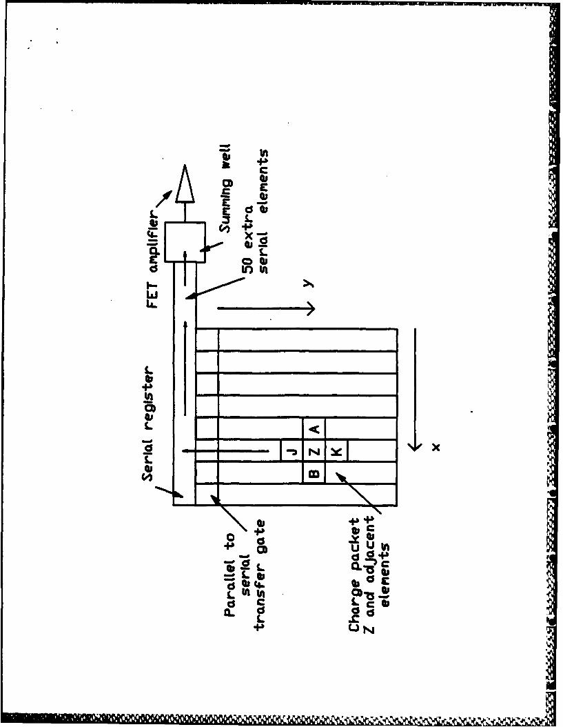
smearing of the image. Fig. 6 illustrates the path that a particular
charge packet takes during charge readout. The transfer process is
divided into those which move charge in the parallel shift direction
and those which move charge in the serial shift direction. The
overall parallel transfer of charge is further divided into the CTE
associated with transfer of charge in the imaging region and the CTE
associated with the transfer of charge from underneath the last
parallel gate to the serial register. This distinction is necessary
because of the different gate structure present in the Tektronix CCI)
used to transfer charge from the last parallel gate to the serial
register. The number of parallel transfers each charge packet may
take is dependent upon its distance from the serial register.
Referring to Fig. 6, for a charge packet located at element Z with
coordinates x and y, the overall parallel CTE is;
CTEparallel - CTE._>s * CTEp 3y 8)
where C7Ep__> s is the CTE associated with the parallel to serial
transfer step, and CTEp is the CTE of the parallel region. The factor
of 3 is for the 3 transfers of charge in a 3 phase device when moving
charge from one pixel to the next. The equation describing the
overall serial CTE is;
CTE ia = CTE_ * CTE3 (x + 50) (9)seil s-->sw 0
where CTE > is the CTE associated with the transfer between the
last serial gate and the output summing well, CTE is the average CTE
of charge transfer in the serial register. The 50 accounts +or the
17
extra 50 elements added to the serial register to separate the output
amplifier from the gates of the image area. Both Eqs. (8) and (9)
include a position dependent and position independent component which
can be distinquished qualitatively from each other by visual
inspection of an image. For example, in an image with poor parallel
CTE, trailing of charge which increases as a function of distance from
the serial register is indicative of a problem with the CTE of the
parallel region. Hoover, for images where the trailing of charge in
the parallel direction is constant across the CCD, the cause of poorS
CTE is the single charge transfer step from the parallel to serial
region.
Ideally, if the e'ectron cloud from the absorption of an x-ray is
always collected in one detector element with no lateral diffusion and
readout with unity charge transfer efficiency, the image would be a
single point with no charge in adjacent elements. However, because
the electron cloud is not always collected in a single potential well,
the charge will be distributed among adjacent elements. On the
average, the amount of charge should initially be equal in the
elements which preceed and trail the x-ray peak. During readout, some
charge in the x-ray peak is left behind and accumulates in the
trailing elements, thus the trailing pixel has slightly more charge
than the pixel preceeding the x-ray peak. The amount of asymmetry in
the imagb of the x-ray absorption is an indication of the charge
transfer efficiency from preceeding to following elements. By
measuring the amount of trailing from x-rays in both directions from
• 11different areas of the CCD, values of CTE for the various transfer
steps in the CCD are extracted.
CTE was measured at the moderately low charge level of 1620 e-
55using an Fe radioactive source which emits 5.9 Key Mn K-alpha
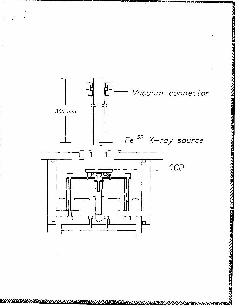
x-rays. The source is mounted in a steel cylinder and rod assembly as
shown in Fig. 7, which allows positioning the source 1 to 250 mm from
the CCD surface. By changing the x-ray source to CCD distance the x-
ray flux can be conveniently adjusted. CTE was determined by
measuring the trailing of charge from detector elements which had
absorbed an x-ray. For each 2 second exposure to the Fe 5 5 source, x-
ray events were identified and their location, intensity, and the
intensity of detector elements adjacent to it in both the serial and 4 .
parallel transfer direction were recorded. A total of 64 exposures
wore taken in order to acquire enough events to calculate CTE. The
identification of x-ray events was accomplished by searching for
pixels whoe intensity ranged between 50 to 100 % of the maximum
charge possible from the complete absorption of a 5.9 Kev x-ray.
Detector elements adjacent to pixels which satisfied the above
condition were limited to values between -5 to 25 % of the total
charge possible from one x-ray. Limiting the x-ray events to those
which satisified the above two conditions was designed to restrict the
data to x-ray events where most of the electron cloud was collected by
a single detector element. This screening helped to simplify the CTE
analysis and improve the overall accuracy of the CTE measurement.
Only small subarravs of the CCD were read to keep the readout time
short compared to the integration time. The location of the subarray
19
was moved to each corner of the CCD in order to realize both the
maximum and minimum number of transfers in both the serial and
parallel shift directions.
CTE values which describe the average parallel and serial
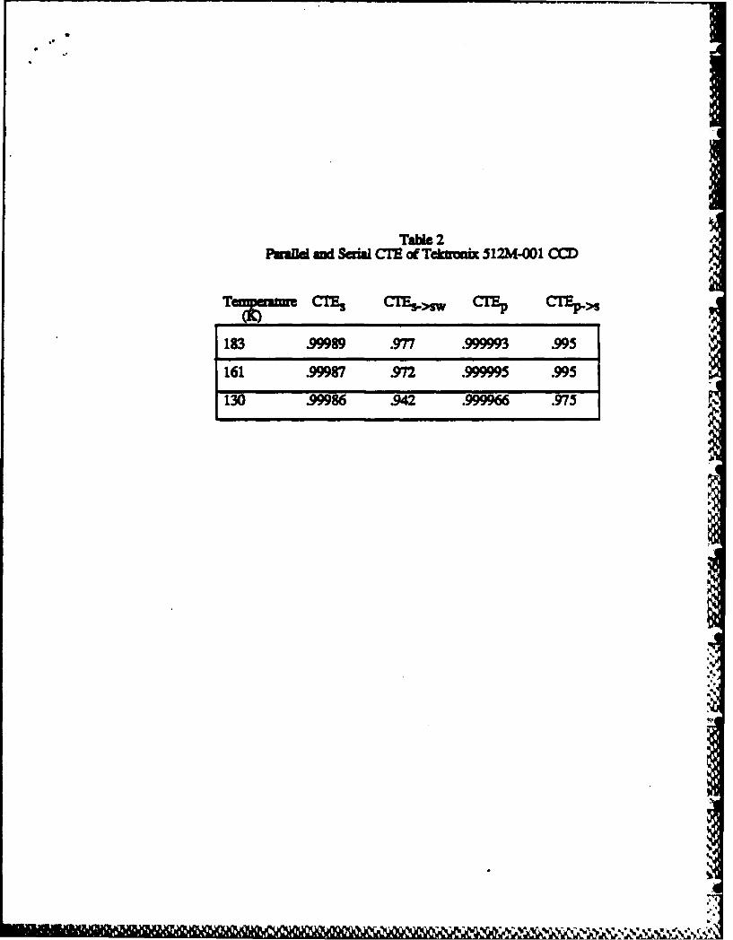
transfer of charge are shown in Table 2 as a function of temperature.
CTE in both the serial and parallel directions tends to degrade as the
temperature is lowered. The parallel CTE is excellent and results in
images which have no discernible streaking of charge in the parallel
shift direction. The serial CTE is quite poor and causes streaking in
the serial direction even from the corner of the CCD nearest the
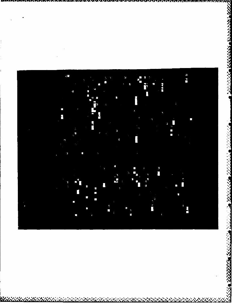
output amplifier as seen in Fig. 8. This behaviour indicates that
there is poor charge transfer between the last serial element and the
summing well of the ouput amplifier.
8. BLOOM ING MEASUREMENTS
Onset of blooming in a CCD occurs when the maximum number of
photogenerated charge carriers which can be collected in one detector
element and transferred to the floating diffusion of the output
amplifier is exceeded. Because of the unique readout mode of a
two-dimensional CCD, charge initially generated in the image region is
transferred through several different regions before being sensed at
the output node, and thus blooming can occur in several different
areas.
Blooming measurements are important in determing the device
performance at high illumination levels. For example, when using a
20
CCD as a detector at the focal plane of a spectrograph, blooming is a
serious and sometimes limiting factor in measuring spectra with both
intense and weak spectral lines (12). Blooming effects can be
mfnimized by orienting the spectral lines in the parallel shift
direction, such that if blooming occurs it will happen along the
direction of the slit and not in the direction of wavelength
dispersion. The above technique is effective only if the charge
capacity of the serial register is equal to or larger than the
parallel register, as is usually the case for most CCDs.
To measure the blooming in the three regions of the CCD, a point
source of visible light was imaged onto a detector element and its
response and the response of adjacent detector elements as a function
of illumination level were monitored. Blooming was determined by
noting the illumination level at which any detector element showed a
sudden increase in signal caused by charge spilling into it from an
adjacent oversaturated detector element. Monitoring the response of
the adjacent elements in addition to the central element is important
for two reasons. First, it provides a more accurate estimate of
blooming onset than simply measuring the saturation point of the
brightest element. When the majority of light is focused onto a
single central element, the rate of increase of an adjacent pixel is
much sharper than the rolloff of the central element's response at the
onset of saturation. Second, by monitoring the response of adjacent
elements in both the serial and parallel shift direction, the
direction of charge blooming is determined.
21
The light source was a 25 micron pinhole illuminated with 600 nm
light focused onto the CCD with a 50 mm f/2 lens and a *3 extension
tube. The gain of the analog to digital electronics was decreased for
blooming measurements to 64 electrons /ADU while measuring blooming in
the serial and parallel registers, and 640 electrons/ADU while
measuring the summing well capacity. In order to measure the serial
register and the summing well blooming, charge binning was used to
transfer a sufficient amount of charge into each well without being
limited by the well capacity of a previous region of the CCD. For
example, in order to measure the blooming caused by exceeding the
charge capacity of the summing well, a larger defocussed pinhole image
was binned 32 fold in both the serial and parallel shift directions.
Therefore each element of this binned image was composed of the charge
from 1024 pixels. The ability to combine charge at the summing well
made it possible to isolate and measure the much larger summing well
capacity. In a similar fashion, charge from several pinhole images
was binned into the serial register in order to isolate and quantitate
blooming in the serial register.
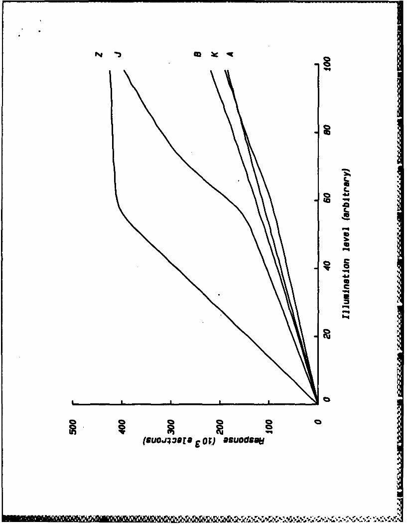
The response from -a typical blooming measurement is plotted in
Fig. 9 and describes the response of the central and four adjacent
detector elements as a function of illumination level of the central
element. Note the response of the central pixel Z saturated at the
same illumination level as the the response of a pixel adjacent to Z
showed a sudden increase in slope (in this case indicating blooming in
the parallel register). Results of the blooming measurements of the
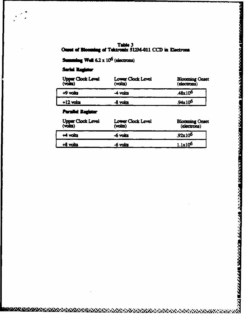
Tektronix 512M-011 are listed in Table 3. As expected, the onset of
22
blooming depends strongly upon gate potentials, increasing as the
upper gate potentials are raised. The summing well saturates at6[
6.2x10⁶ electrons, beyond which charge can no longer be binned into
the summing well and spills back into the serial register. A charge
storage capacity of this magnitude along with a read noise of 6
electrons yields a dynamic range of greater than 106 when using this
CCD in a highly binned readout mode.
Blooming usually occured in the serial register before the
parallel register for most of the gate voltages investigated. The
maximum amount of charge which could be contained in the serial
register before blooming occured was 940,000 electrons, and occured
at the maximum serial clock voltage swing of -8 to +12 volts.
Blooming in the parallel register was difficult to measure at most
clock levels investigated for two reasons. The first is that charge
first bloomed in the serial direction, rather than the parallel
direction for most clock voltages for this particular CCD. Blooming
in the parallel register was determined by going past the point at
which the central element bloomed in the serial direction until the
device bloomed into pixels adjacent to the central element in the
parallel direction. The second problem with measuring parallel
register blooming was that when the high parallel clock level exceeded
+5 volts, and the charge in any pixel reached 400,000 electrons,
streaking occurred in the serial direction. The streaks began
immediately after the bright pixel with the intensity showing an
exponential decay in the serial direction. The smearing of bright
detector elements disappeared when the high parallel clock was reduced
23
to below +5 volts and was insensitive to the serial clock voltage
levels. It is believed that this effect is due to a small pocket of
charge trapped in the parallel to serial transfer region which bleeds
into trailing pixels when charge in the serial register is clocked
out.
The optimum gate voltages for this particular Tektronix CCD based
only on these blooming measurements were arrived at by maximizing the
serial and parallel full wells without exceeding the clock voltages
that caused the parallel to serial transfer gate smearing of charge.
At these clock levels blooming in the serial and parallel directions
occurs at approximately the same charge levels and no smearing of
bright pixels in the serial shift direction is observed. It should be
noted that these measurements were made on a single CCD. According to
Tektronix, the gate area devoted to the serial register was designed
to give the serial register twice the full well of the parallel
register. The fact that blooming in the serial register occurs at
charge levels equal or less than the level which causes blooming in
'he parallel registers and that the serial CTE is poor indicate that
ther charge is not being properly contained in the serial register
potential wells or that charge is not being efficiently transferred
from the serial register into the output summing well.
9. LATENT IMAGE OBSERVATIONS
During initial investigations into the imaging properties of the
TK512-011 frontside-illuminated CCD, an effect was observed in which a
I- .'**:°
24
previously recorded image would reappear to a small degree in a later
readout. Several qualitative experiments were conducted to attempt to
understand the mechanism of this effect. In a typical experiment, the
CCD was operated in the slow-scan camera cooled to -100C. A test
pattern illuminated with 800 nm radiation was imaged on the CCD until
the highlight areas were at approximately 1/4 full well. The shutter
was closed and the CCD was read out, then immediately read out again.
In the second read, there was no evidence of a latent image. Next,
the CCD was allowed to integrate charge in the dark for 60 seconds,
then read out a third time. In this read, a latent image identical to
the test pattern with approximately 7 electrons RMS in the highlight
areas was observed.
Latent image effects have been observed to varying degrees of
severity in all Tektronix frontside illuminated CCDs characterized in
these laboratories. This effect has also been observed by other
investigators.** This phenomenon can arise from two possible
mechanisms: charge arising from interface states at the Si-SiO 2
interface, and charge arising from defects in the epitaxy-substrate
junction. Charge trapped in either of these interfaces will slowly
be released back into the conduction band. Any released charge which
is subsequently accumulated in the potential wells of the imaging
array contribute to a latent image.
These mechanisms account for the observation that latent images
do not appear immediately after a high level image is read, but "grow"
slowly as the- CCD integrates charge. The rate of release from the
trap zone is very slow at -100C as latent image generation has been
. . , . . . .. . . . + .. .. . . . + 5 . . .. + . .... .. .
25
observed to persist for many minutes after initiation. The second
mechanism accounts for the observation that long wavelength photons
are neccesary to initiate a latent image. Only longer wavelengths can
pentrate deep enough to generate charge near the epitaxy-substrate
junction.
* Footnote 1. J.R. Janesick, JPL and Harry Marsh, Tektronix, personal
communications.
10. CONCLUSIONS
The evaluation of the TEK512M-O11 frontside-illuminated 512 by
512 element CCD shows it to be a promising detector for scientific
applications. Table 4 is a summary of these evaluation results. The
output FET exhibits a noise floor equivalent to 5 to 12 electrons
depending on the integration time of the dual slope analog processor.
Additionally, the optimal FET operating conditions are not critical
functions of temperature,* drain to source voltage or drain current.
The electro-optical characterization reveals extraordinary performance
in many respects, as well as several problems in the device which need
improvement. Very good low light level CTE is observed in the
parallel shift register. However, poor serial CTE is observed in the
serial direction partially due to difficulties in transferring charge
to the output amplifier. The quantum efficiency observed for this
device is lower than expected. Finally, a extremely slight latent
image effect is observed under certain conditions. Some of the
1111,1 11 IN ,L lil~li 1111111111111 11 111 1
26
encouraging characteristics of the device tested are excellent
linearity, very high dynamic range, and low dark current. In general,
the TK512M-011 has the potential to be an excellent scientific image
sensor.
It is important to realize that these results are from the
characterization of a limited number of preliminary CCDs. It is
expected that in the near future, devices will be available with
significantly improved electro-optical characteristics. The
evaluation of the frontside illuminated TK512M-011 CCD has importance
to the larger CCD arrays being introduced by Tektronix. These devices
have the same FET preamplifers and same geometry detector elements,25
thus many of the results of the evaluation of the 5122 CCD will apply
to the 10242 and 20482 format CCDs. Initial work in these
2laboratories with a 2048 device indicates great similarities in
operating conditions and imaging performance between the two
detectors.
The introduction by Tektronix of an entire line of CCDs designed
exclusively for scientific applications has great importance for the
scientific CCD imaging community. The demand for CCD imaging systems
for scientific use is increasing rapidly, while the number of
manufacturers of commercial scientific grade CCDs is decreasing. The
continued availability of commercial CCDs rests with the introduction
of CCD sensors by such companies as Tektronix, Reticon, Thomson-CSF,
and Kodak.
VN

t. ACKNOWLEDGMENTS
The research reparted in this paper was partially funded by the
National Aeronautics and Space Administration (Contract No. NAS 5-29284)
and the Office of Naval Research. We wish to thank Jack Orach and Keith
Copeland for assistance in the design and construction of the CCD test
fixtures.
b
- C ~ '~
12. REFERENCES 1 to 15
1) J. Janesick, T. Elliott, S. Collins, H. Marsh, M. Blouke, and J.
Freeman, "The future scientific CCD," in State-of-the-Art Imaging
Arrays and Their Applications, K. Prettyjohns, ad., Proc. SPIE 501, 2-
31 (1994).
2) J. B. Oka, "Low and moderate resolution spectroscopy with an RCA
charge-coupled device (CCD)," in Solid State Imaaers for Astronomy, J.
Geary and D. Latham, ads., Proc. SPIE 290, 45-50 (1981).
3) J. Janesick, D. Campbell, T. Elliott, T. Daud, P. Ottley, "Flash
technology for CCD imaging in the UV," in IN Technology, R. Huffman,
ed., Proc. SPIE 687, 36-55 (1996).
4. A. Fowler, P. Waddel, L. Mortara, "Evaluation of the RCA 512X320
charge-coupled device (CCD) imagers for astronomical use," in Solid
State Imaoers for Astronomy, J. Geary and D. Latham, eds., Proc. SPIE
290, 34-44 (1991).
5) W. S. Boyle, G. E. Smith, "Charge Coupled Semiconductor Devices,"
Bell System Tech Journal 49, 587-593 (1970).
6. G. F. Amelio, M. F. Tompsett, G. E. Smith, "Experimental
Verification of the Charge Coupled Device Concept," Bell System
Technical Journal 49, 593-600 (1970).
7) 11. Mt. Blouke, D. L. Heidtmann, B. Corrie, M. L. Lust, J. R.
Janesick, "Large area ccd image sensors for scientific applications",
in 31alid State Imaging Arrays, K. Prettyjohns, E. Dereniak, eds.,
Proc. SPIE 570, 82-89 (1995).
9) N. S. Saks, "Interface state trapping and dark current generation
in buried channel charge-coupled devices", 3. Appi. Phys. 53(3), 1745-
1753, (1992).
9) N.S. Sake, "A Technique for suppressing dark current generated by
Interface states in buried channel CCD imagers", IEEE Electron Device
Letters, EDL-1(7), 131-133, (1980).
10) ?I. Blouke, 3. Janeslck, J. Hall, and M. Cowens, nTexas Instruments
(TI) 900X800 charge-coupled device (CCD) image sensor", in Ug0 t~
IMAoers for Astronomy, J. Seary and D. Latham, ads., Proc. SPIE 290,
6-15 (1991).
11) EEV Technical Note 1(1), "Basic Operation of a CCD Frame Transfer
Array",(1982), Essex, England.
12) M. B. Denton, H. A. Lewis, and G. R. Sims, "Charge-injection and
charge-coupled devices in practical chemical analysis," in
Mltichannel Imagm Detectors, afi Symposium Series, Y. Talmi Ed., 2,-
13Z-154 (1983).
13) TH7841 Data Shoot, Thowsan-CSF, Codex, Francs, (1983).
14) S. Vogt, R. Tull, P. Kelton, "Solf-scanned photodiode arrays high
performance operation in high dispersion astronomical
spectrophotometry," Imlid Oticm 17, 574-592 (1978).
15) J. Janesick, T. Elliott, S. Collins, T. Daud, D. Cambell, A
Dingizian, 9. Garmire, "CCD advances for X-ray scientific measurements
in 1985," in X-ray Instrumentation for AMtronomy, J. Culhane, ed.,
Proc. SPIE 597, 364-380 (1995).
0
S_
'S
Sq ~ ~ ~ 5 *~% '~ *0 -. 'S 9 V I'
~ ~.- =
>L
Iis
IIn
S -U
UCU-*xl Sao c
4,b a
C -spmw>
FLI
cm)k
C.S
C.S
SS
4..SCU
'.4
p p p p p p p
* III(UUO.J~3W[9 E0~ *suods.ef
Lw,
I0
cu c
(286-&) zoi unO3vill 60-
CCC
Ca
IA
NS
S
S
CCI0
I
CC
C C
WnwwrIo z
- - ,
-I;LC
LaiIL
+1
0 ~4 C -
L 41(
5 - L -.
C-
+1 UN
P Vacuum connector
300 MM
Fe 55 X-ray source
Ll.
CCD ~ C~
at
Jb
S.
a.
U
p
Lb
4
#'
-T'p
Pb
P.p.
Pt.x
V
r44
U 1'-A
b-igg, ..- ~ t * -r -.~ w *~*~ *.~ xq ~ ~N9 &: ~ ~&:~- ~Z Z~Z&Z:4~2? kQt~ kN§ ~
N *'~
'ml
I..UC.
~ .6.9La
.0C-S
S
Spm,
4.S*uqS
6-I
p p I I
0 C C 0 0C C
~1I 'ml(suo.J;3e(9 £ O~) asuods.I~
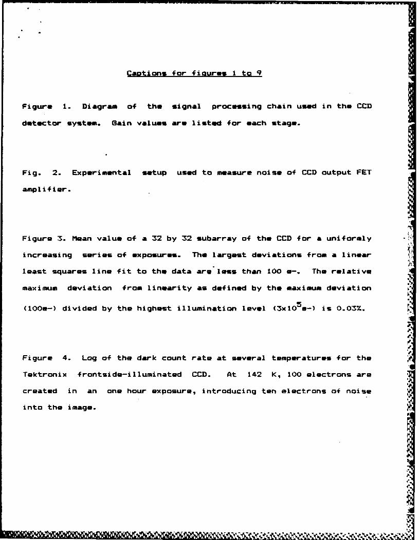
Caations for fioures 1 to 9
Figure 1. Diagram of the signal processing chain used in the CCD
detector system. Gain values are listed for each stage.
Fig. 2. Experimental setup used to measure noise of CCD output FET
amp l i f ier.
Figure 3. Mean value of a 32 by 32 subarray of the CCD for a uniformly
increasing series of exposures. The largest deviations from a linear
least squares line fit to the data are less than 100 a-. The relative
maximum deviation from linearity as defined by the maximum deviation
(100e-) divided by the highest illumination level (3 x1O5e-) is 0.03%.
Figure 4. Log of the dark count rate at several temperatures for the
Tektronix frontside-illuminated CCD. At 142 K, 100 electrons are
created in an one hour exposure, introducing ten electrons o noise
into the image.
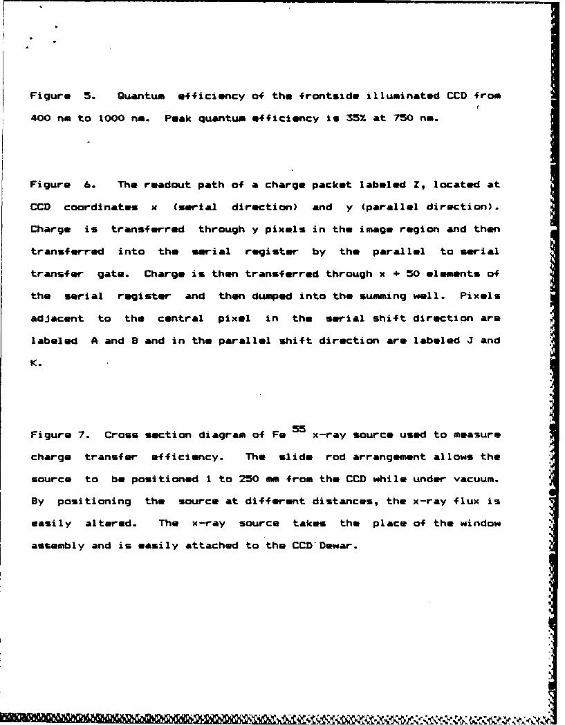
Figure 5. Quantum efficiency of the frontside illuminated CCD from
400 no to 1000 no. Peak quantum efficiency is 35% at 750 n.
Figure 6. The readout path of a charge packet labeled Z, located at
CCD coordinates x (serial direction) and y (parallel direction).
Charge is transferred through y pixels in the image region and then
transferred into the serial register by the parallel to serial
transfer gate. Charge is then transferred through x + 50 elements of
the serial register and then dumped into the summing well. Pixels
adjacent to the central pixel in the serial shift direction are
labeled A and B and in the parallel shift direction are labeled J and
K.
Figure 7. Cross section diagram of Fe x-ray source used to measure
charge transfer efficiency. The slide rod arrangement allows the
source to be positioned 1 to 250 mm from the CCD while under vacuum.
By positioning the source at different distances, the x-ray flux is
easily altered. The x-ray source takes the place of the window
assembly and is easily attached to the CCD'Dewar.
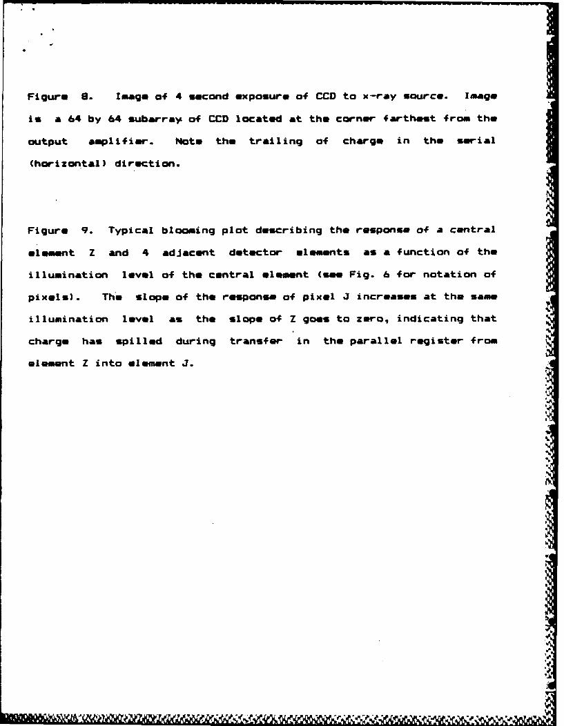
Figure 8. Image of 4 second exposure of CCD to x-ray source. Image
is a 64 by 64 subarray of CCD located at the corner farthest from the
output amplifier. Note the trailing of charge in the serial
(horizontal) direction.
Figure 9. Typical blooming plot describing the response of a central
element Z and 4 adJacent detector elements as a function of the
illumination level of the central element (see Fig. 6 for notation of
pixels). The slope of the response of pixel J increases at the same
illumination level as the slope of Z goes to zero, indicating that
charge has spilled during transfer in the parallel register from
element Z into element J.
-,
A
b
..
'I.
Table ICCD IET Amplifier Typical Analyzed Data Set
Vd V Vs Gfs Gan Rout En FOM n Elecusvolts v! volts mho ohms dbv Ms
22 1.2 6.17 220 0.81 3704 -120.0 118.22 18.26 10.34
20 1.2 6.15 220 0.81 3704 -122.0 120.22 14.50 8.21
18 1.2 6.12 220 0.81 3704 -123.0 121.22 12.93 7.32
16 1.2 6.11 210 0.81 3846 -124.0 122.14 11.52 6.52
14 1.2 6.09 200 0.80 4000 -125.5 123.56 9.96 5.49
12 1.2 6.07 180 0.78 4348 -127.0 124.87 8.16 4.62 -
10 1.2 6.04 180 0.78 4348 -126.5 124.37 8.64 4.89
8 1.2 6.00 160 0.76 4762 -126.5 124.14 8.64 4.89
°,
'
,r. C -~ ~A~ A
Tabe 2PuiWe and Sedda CI'E of Teinix 512M-001 CCI)
T=.~M-- C1TE5 CTE3>Sw CrEp CrE.>S
183 .99989 Y"7 .999993 .995
161 .99987 -972 .999995 .995
130 .99986 -942 .966 .975
Tabl 3Omr o Womn of. OT*bviZ 512M411 CCD in E~dram
Smdg Wd 6.2 x 10⁶ (deum.)
8em Rhemer
Cloc Land Low Clock LAv kx~n ne
9 b-4 voks .48xl10 6
+12 valt 4 valis .94xj06
Pa RqOWw
0M~o* Lavei Lower Clock Level BlOoming Quie
44 voi -6 voks .92x106
44vk 4~ 6val 1.1xI 0 6
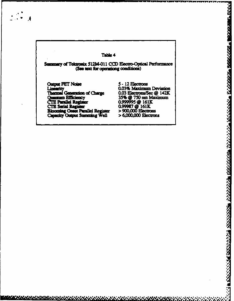
Table 4
Smw of Tekuuix 512M-011 CCD macaD-Op"ia PUffOIinZC(Sem nfr opomiong cmddma)
Oiupm PET Ndwu 5 -12 MlecumonLinidtv0.03% Maximum Deviation
cmaxionat bwp 0.03 Elecuons(Sec @ 142K~~mu~FlIemCW 35% @ 750 =r Mimm
Raj gwium 0.999995Q 161KcIE Sail agu 0.9997 161K
B~~aPe >in Paa~js 90000 ElectronCqtiy uatSumning wl > 6,000,000 mactra
%1% 1: lz
/
I


![Supplementary Material: Dynamic Graph Message Passing …openaccess.thecvf.com/content_CVPR_2020/...(OHEM) [26, 23, 15, 30, 28], Multi-Grid [2, 10, 4] and Multi-Scale (MS) ensembling](https://img.pdfslide.us/doc/110x75/5fa0c7e32ef59536976a3efd/supplementary-material-dynamic-graph-message-passing-ohem-26-23-15-30.jpg)