Embed Size (px)
Citation preview

July 21, 2006 17:36 00007 none
NANO: Brief Reports and ReviewsVol. 1, No. 1 (2006) 1–13c© World Scientific Publishing Company
ELECTRICAL TRANSPORT PROPERTIESAND FIELD EFFECT TRANSISTORS
OF CARBON NANOTUBES
HONGJIE DAI*, ALI JAVEY, ERIC POP, DAVID MANN,WOONG KIM and YUERUI LU
Department of Chemistry and Laboratory for Advanced MaterialsStanford University, Stanford, CA 94305, USA
Received 30 May 2006
This paper presents a review on our recent work on carbon nanotube field effect transistors,including the development of ohmic contacts, high-κ gate dielectric integration, chemical func-tionalization for conformal dielectric deposition and pushing the performance limit of nanotubeFETs by channel length scaling. Due to the importance of high current operations of electronicdevices, we also review the high field electrical transport properties of nanotubes on substratesand in freely suspended forms. Owing to their unique properties originating from their crystalline1D structure and the strong covalent carbon–carbon bonding configuration, carbon nanotubesare highly promising as building blocks for future electronics. They are found to perform favor-ably in terms of ON-state current density as compared to the existing silicon technology, owingto their superb electron transport properties and compatibility with high-κ gate dielectrics.Future directions and challenges for carbon nanotube-based electronics are also discussed.
Keywords : Carbon nanotubes; FETs; ballistic transport; phonon scattering; thermal transport;contacts.
1. Introduction
Much progress has been made recently showingthat single-walled carbon nanotubes (SWNTs) areadvanced quasi-1D materials for future high per-formance electronics.1–8 SWNT field effect transis-tors (FETs) can outperform state-of-the-art siliconFETs owing to near ballistic electrical transport,chemical robustness, lack of surface dangling bondsand sustained electrical properties when integratedinto realistic device structures. The strong covalentC–C bonding and lack of surface dangling bonds arethe fundamental reasons underlying the advancedproperties of carbon nanotubes and high potentialfor future electronics. In this review, we present ourrecent progress in developing Ohmic contacts, gate
dielectric integration and channel length scaling forSWNT FETs.
Ever since the beginning of the integrated cir-cuit era, aggressive scaling of the device elementshas been actively pursued in order to increase thespeed and density. The end of this “evolutionary”path, however, is only a decade or so away due tothe physical and technical limitations of the cur-rent technologies. Beyond this scaling limit, shortchannel effects and high leakage currents severelydegrade the performance of the conventional de-vices so that they can no longer operate properly.9
“Revolutionary” concepts, therefore, need to be de-veloped for further miniaturization of digital com-ponents down to the molecular scales.
As the conventional CMOS technology reachesits scaling limit, many have approached novel
1

July 21, 2006 17:36 00007 none
2 H. Dai et al.
concepts, such as nanotube-based electronics, asalternatives. Carbon nanotubes are molecular-scale (∼ 1 nm diameter) wires with atomicallywell-defined structures.1–3 They are ideal for eluci-dating basic phenomena in 1D and have been pro-posed as the potential building blocks for futurenanoelectronics. SWNTs can be thought of as 2Dgraphene sheets that are wrapped around to form1D cylinders.1–3 They are composed of only C–Csp2 bonds, which are among the strongest chemi-cal bonds, making them unique structures that arechemically inert, electrically stable, and mechani-cally robust. With diameters d = 0.5–5 nm andlengths L = ∼ 10 nm to ∼ 1 cm, nanotubes areperhaps the closest known materials to ideal 1Dstructures. Nanotubes are mainly characterized bytheir wrapping vector Rnm = (n,m) = na1 + ma2,which refers to the folding of the graphene sheet asshown in Fig. 1(a). The wrapping vector governsthe electrical characteristics of nanotubes, whichcan be either metallic or semiconducting (Figs. 1(b)and 1(c)) with band gaps inversely proportional to
the diameter.1–3 There are virtually unlimited num-ber of possibilities for the chirality and diametercombination of nanotubes, making them a novelclass of materials with a wide spectrum of prop-erties and potential applications in electronics.
2. Achieving Zero Schottky BarrierMetal Contacts for NanotubeFETs
SWNT FETs were first demonstrated by Dekkerand coworkers,10 and by researchers at IBM11 andStanford.12 Like any materials for potential elec-tronic applications, achieving Ohmic contacts is thekey to high device performance. The existence of“barriers” (not specifically named “Schottky bar-riers”) between metal contacts and SWNTs, andthe resulting thermally activated transport were ini-tially reported by Zhou et al.13 A correlation be-tween the barrier height and SWNT diameter wasalso noted.13 Later, systematic work by researchers
(10,10)
a2
Rnm = (n,m) = (11,7)
a1
(a)
(10,10) armchair metallic
(11,7) chiral
semiconductor
(b) (c)
Fig. 1. Folding of graphene into nanotubes. (a) Various chiralities of carbon nanotubes can be obtained by folding alongdifferent wrapping vectors Rnm. (b) and (c) are schematics of (10, 10) and (11, 7) nanotubes. A (n, m) tube is metallic whenn = m (armchair). A nanotube with n−m = 3j, where j is an integer, is a semi-metal with a curvature-induced band gap onthe order of few meV. A nanotube is semiconducting when n − m = 3j.

July 21, 2006 17:36 00007 none
Electrical Transport Properties and Field Effect Transistors of Carbon Nanotubes 3
at IBM further established the existence of Schottkybarriers (SBs) between SWNTs and metals (e.g.,Ti).14 It is now well accepted that in many cases,SBs exist between metal contacts and quasi 1DSWNT semiconductors. How to overcome, reduceor eliminate this barrier to achieve Ohmic contactsto semiconducting nanotubes has been actively pur-sued by researchers in recent years. Progress hasbeen made but challenges remain.
In order to understand the intrinsic electrontransport physics of carbon nanotubes and exploretheir device performance limits, it is essential toform near-Ohmic contacts without any significantscattering or energy loss of the carriers at thesource/drain (S/D) interfaces. It is difficult to formOhmic metal contacts to intrinsic planar Si chan-nels due to the Fermi-level pinning. It is widely be-lieved that the metal-induced gap states (MIGS) atthe metal–semiconductor interfaces, which result inplanar dipoles, pin down the Schottky barrier (SB)heights and make them nearly independent of the
contact metal work function.15 For a 1D channel,such as carbon nanotubes, however, the dipole layerthat is created at the metal–channel interface dueto MIGS has a “molecular” scale (nearly 0D) withdifferent electrostatics than the planar dipoles.16
Unlike the planar dipoles where the potential isconstant outside of the dipole layer, in “molecular”-scale dipoles, the potential decays to zero in regionsfar away from the S/D interfaces. As a result, in 1Dnanotube devices, MIGS do not induce a strong pin-ning of the Fermi-level, and therefore the Schottkybarrier heights are primarily governed by the en-ergy difference of the work function of the metalcontacts and the conduction/valance band edge ofthe nanotubes.
Based on this principle, zero SB contacts to thevalence band of chemically intrinsic nanotubes withdiameter d>∼ 1.6 nm (band gap Eg <∼ 0.6 eV)have been experimentally demonstrated using highwork function palladium (Pd, Φm ∼ 5.0 eV) asthe electrode material (Figs. 2(a) and 2(b)). These
(a) (c)
(b) (d)
Fig. 2. Pd-contacted and back-gated SWNT-FETs on Si/SiO2 (tox ∼ 500 nm) substrates. (a) Scanning electron microscopy(SEM, left) and atomic force microscope (AFM, right) images of a SWNT bridging three Pd contacts. (b) Schematic viewof a device. (c) Transconductance G versus Vgs for a 300-nm long tube device at various temperatures. Differential conduc-tance dIds/dVds versus Vds and Vgs (inset) at T = 1.5 K shows a Fabry–Perot-like interference pattern, a hallmark of ballistictransport. (d) ON-state conductance as a function of temperature for the same device.
July 21, 2006 17:36 00007 none
4 H. Dai et al.
nanotubes are capable of delivering high current(µA) densities at relatively low bias voltages.5
The ON-state of the Pd-contacted p-FETs ex-hibits metallic-like behavior, with the low-bias con-ductance linearly increasing as the temperature islowered due to the freezing of acoustic phonons(Figs. 2(c) and 2(d)). At cryogenic temperatures,the ON-state conductance approaches the quantumconductance limit of G0 = 4e2/h (Fig. 2(c) inset),implying a ballistic device without any significantscattering of the carriers in the nanotube channelor at the S/D contact interfaces. This is in clearcontrast to the SWNT SB-FETs (for example, Ti-Ni- and Cr-contacted FETs) that become nearlyinsulating at low temperatures as the thermionicemission and thermally assisted-tunneling compo-nents of the carrier injection vanish. The lack ofpositive Schottky barriers at the contacts is a criti-cal step for achieving state-of-the-art SWNT FETsthat operate near the performance limit of an ideal1D system.
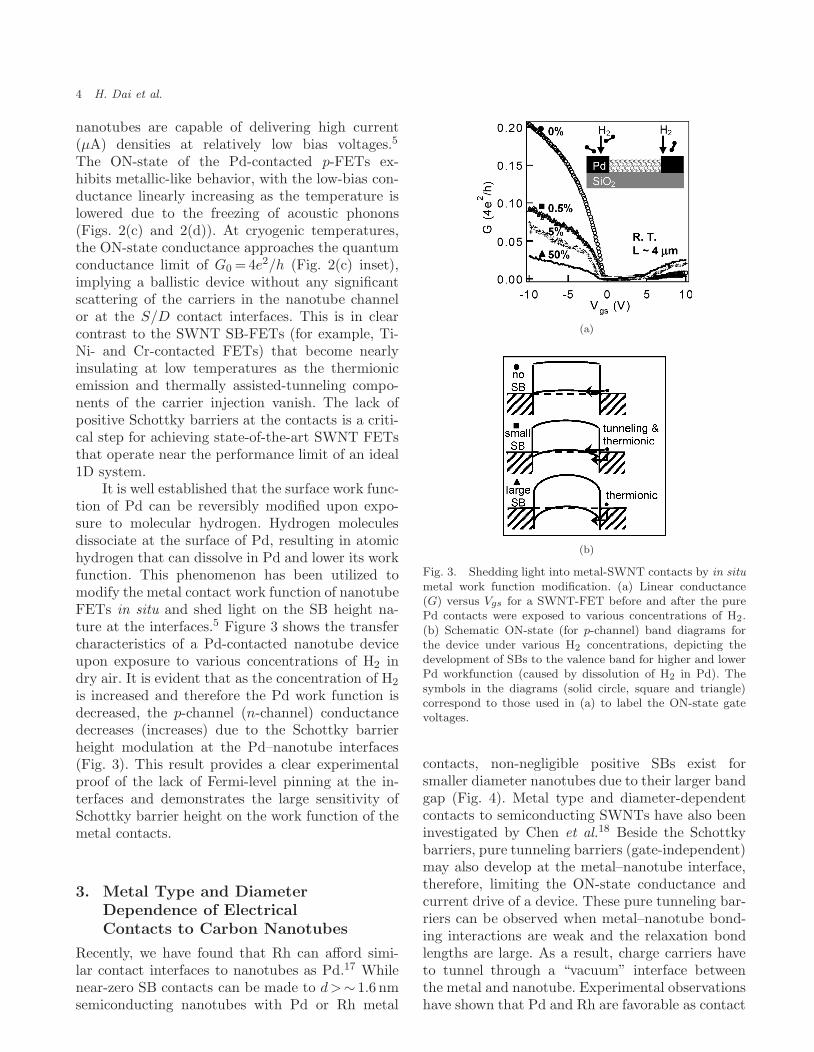
It is well established that the surface work func-tion of Pd can be reversibly modified upon expo-sure to molecular hydrogen. Hydrogen moleculesdissociate at the surface of Pd, resulting in atomichydrogen that can dissolve in Pd and lower its workfunction. This phenomenon has been utilized tomodify the metal contact work function of nanotubeFETs in situ and shed light on the SB height na-ture at the interfaces.5 Figure 3 shows the transfercharacteristics of a Pd-contacted nanotube deviceupon exposure to various concentrations of H2 indry air. It is evident that as the concentration of H2
is increased and therefore the Pd work function isdecreased, the p-channel (n-channel) conductancedecreases (increases) due to the Schottky barrierheight modulation at the Pd–nanotube interfaces(Fig. 3). This result provides a clear experimentalproof of the lack of Fermi-level pinning at the in-terfaces and demonstrates the large sensitivity ofSchottky barrier height on the work function of themetal contacts.
3. Metal Type and DiameterDependence of ElectricalContacts to Carbon Nanotubes
Recently, we have found that Rh can afford simi-lar contact interfaces to nanotubes as Pd.17 Whilenear-zero SB contacts can be made to d>∼ 1.6 nmsemiconducting nanotubes with Pd or Rh metal
(a)
(b)
Fig. 3. Shedding light into metal-SWNT contacts by in situmetal work function modification. (a) Linear conductance(G) versus Vgs for a SWNT-FET before and after the purePd contacts were exposed to various concentrations of H2.(b) Schematic ON-state (for p-channel) band diagrams forthe device under various H2 concentrations, depicting thedevelopment of SBs to the valence band for higher and lowerPd workfunction (caused by dissolution of H2 in Pd). Thesymbols in the diagrams (solid circle, square and triangle)correspond to those used in (a) to label the ON-state gatevoltages.
contacts, non-negligible positive SBs exist forsmaller diameter nanotubes due to their larger bandgap (Fig. 4). Metal type and diameter-dependentcontacts to semiconducting SWNTs have also beeninvestigated by Chen et al.18 Beside the Schottkybarriers, pure tunneling barriers (gate-independent)may also develop at the metal–nanotube interface,therefore, limiting the ON-state conductance andcurrent drive of a device. These pure tunneling bar-riers can be observed when metal–nanotube bond-ing interactions are weak and the relaxation bondlengths are large. As a result, charge carriers haveto tunnel through a “vacuum” interface betweenthe metal and nanotube. Experimental observationshave shown that Pd and Rh are favorable as contact

July 21, 2006 17:36 00007 none
Electrical Transport Properties and Field Effect Transistors of Carbon Nanotubes 5
20
15
10
5
-Ion (
µA)
2.52.01.51.0d (nm)
Metallic Semiconducting
Fig. 4. Diameter-dependent electrical properties of metal-lic and semiconducting SWNTs. Room temperature Ion (de-fined as the current under |Vds| = 1 V) versus d plots for bothmetallic and semiconducting SWNT devices with Rh or Pdcontact (similar results for both metals).
materials over other high work function metals suchas Au and Pt. This may in fact be due to the largerbonding interactions between Pd/Rh and nanotubeas compared to Pt and Au, although more detailedexperimental and theoretical work is still neededto better understand the precise nature of thisobservation.
A surprising observation is that the contactresistance between Pd/Rh electrodes and metallicnanotub es is also found to be diameter-dependentfor small nanotubes (Fig. 4).17 Since there are noSBs at the interface for zero band gap metallicnanotubes, the low current drive for d≤∼ 1.0 nmnanotubes is attributed to the development of puretunneling barriers as the chemical reactivity ofnanotubes is known to be diameter-dependent. Theexistence of SBs for small semiconducting SWNTsis responsible for lower currents than in same-diameter metallic tubes. Chemical doping can beinvoked to suppress the positive SBs as demon-strated experimentally.19 However, the tunnel bar-rier appears to be independent of doping andcauses non-Ohmic contact for d< 1.2 nm SWNTs(for semiconducting and metallic tubes alike) evenunder chemical doping. Little is known currentlyabout how to suppress this contact barrier for suchsmall diameter SWNTs. The origin of this tunnelbarrier could be coming from significant alterationof the SWNT structure due to chemical perturba-tions by the contact metal, that is, small nanotubesare chemically more reactive than larger tubes, andthe interaction with metal atoms may give rise toinvasive contact effects that lead to degradation ofthe transport properties of the nanotubes at the
electrodes. This possibility however, requires fur-ther investigation.
Making Ohmic contacts to very small(d ≤ 1 nm) nanotubes is currently a key challengeand requires developing a strategy to eliminate thelarge electrode tunnel barriers. Various chemicalsynthesis methods including HiPco20 and CoMo21
are known to produce very small tubes predomi-nantly in the 0.7–1.2 nm range. An Ohmic contactsolution for down to 0.7 nm tubes will be needed inorder to enable high performance electronics withthese materials. To achieve this goal, systematicexperiments and theoretical understanding will beneeded, including continued search for an optimumcontact material.
4. High-κ Dielectric Integration
Thin films of high-κ materials, such as ZrO2 andHfO2 (κ ∼ 15–25), are highly desirable for gatedielectric integration in field effect transistors asthey enable high ON-state current densities (speed)and low operating power consumptions. The in-tegration of high-κ dielectrics, however, has beena challenge in planar MOSFETs because of theinherent mobility degradation of the Si channels.A unique advantage of carbon nanotubes is theircompatibility with high-κ dielectrics. The lack ofdangling bonds at the nanotube/high-κ interfaceand the weak noncovalent bonding interactions be-tween the two materials, prevent any large pertur-bation of electron transport in carbon nanotubes.4
Figure 5 shows TEM images of suspended (a)and on substrate (b) carbon nanotubes after atomiclayer deposition (ALD) of ∼ 8 nm thick high-κ film.It is evident that high-κ materials do not nucleateon pristine carbon nanotubes,6 except at defect sites(Fig. 5(a)). For nanotube devices on substrates, theALD of high-κ dielectrics initiates on the surround-ing SiO2 substrate and “drowns” the nanotubesonce the thickness of the film surpasses the diame-ter of the nanotube (Fig. 5(b)). As a result, the in-terface bonding between nanotubes and the high-κdielectric is only through weak van der Waals forces,and the intrinsic chemical and physical nature of thenanotubes are well preserved after ALD. However,since as-grown SWNT-derived FETs with high-κdielectrics rely on ALD nucleation and growth onOH-terminated SiO2 substrates, ALD of relativelythick high-κ films (≥ 8 nm) are needed to fully coverthe SWNTs and avoid gate leakage.

July 21, 2006 17:36 00007 none
6 H. Dai et al.
Suspended SWNT
HfO2 film nucleated at a defect site
(a)
SWNT
(b)
Fig. 5. TEM images of (a) suspended and (b) on SiO2
substrate SWNTs after atomic deposition ALD of high-κdielectrics.
Recently, we found that by noncovalentfunctionalization of SWNTs with ploy-T DNAmolecules (dT40), one can impart functional groupsof sufficient density and stability for uniform andconformal ALD of high-κ dielectrics with thick-ness down to 2–3 nm on SWNTs (Fig. 6).22 Thisenables us to approach the ultimate vertical scal-ing limit of nanotube FETs and reliably achieveS ∼ 60 mV/decade at room temperature (Fig. 7).For nanotube FETs without DNA functionaliza-tion, severe gate leakage and shorts were observedfor most FETs with high-κ thickness tox ≤ 5 nm.With DNA functionalization, high performancenanotube/high-κ FETs were reliably obtained withHfO2 down to tox ∼ 2 nm (Fig. 7). These DNA func-tionalized SWNT FETs reproducibly reached thetheoretical limit of S ∼ 60 mV/decade at 300 K(Fig. 7(a)).22 With noncovalent DNA functionaliza-tion, we observed no degradation in the SWNT FET
conductance after the functionalization and subse-quent ALD.
We have carried out microscopy investigationsto understand ALD processes on SWNTs withand without DNA functionalization (Fig. 6). ForSWNTs on SiO2 substrates with DNA functional-ization, we observed concurrent ALD of HfO2 onboth nanotube and SiO2 surfaces, evidenced by thepost-ALD topographic height difference betweenthe nanotube site and surrounding being approx-imately the tube diameter d (Fig. 6(a) left panel).In contrast, for SWNTs on SiO2 without DNAfunctionalization, “grooves” were observed alongthe nanotubes after ALD of HfO2 (Fig. 6(a) rightpanel), indicating the lack of nucleation and growthof HfO2 directly on the tube surface and engulf-ing of the tube by HfO2 grown on the SiO2. Wealso carried out ALD on suspended SWNTs grownon transmission electron microscopy (TEM) grids.With DNA functionalization, suspended SWNTsallowed for quasi-continuous and conformal HfO2
coating by ALD (Fig. 6(b) left image). This differedfrom “balling up” of high-κ material locally on as-grown tubes presumably on defect site (Fig. 6(b)right image).6,23
Our microscopy data provides direct evidenceof active nucleation and growth of HfO2 on the side-walls of DNA functionalized SWNTs in ALD. DNAis known to noncovalently absorb24 on SWNT side-walls via π-stacking25 of the base-pairs. This func-tionalization is found to be thermally stable at theALD temperature of 90C. The functional groups inDNA molecules (OH, phosphate, etc) are involvedin chemisorption of precursor species in the ALDprocess, affording uniform nucleation and growthof HfO2 coating on nanotubes.
The vertical scaling of high-κ dielectrics forSWNT FETs is expected to be useful for investigat-ing interesting device physics in quasi-1D systemssuch as electron tunneling. In a 1D channel, electro-statics are dependent on the gate dielectric thick-ness and the widths of tunnel barriers (Schottky,band-to-band tunneling BTBT,26,27 etc) are oftenset by the gate dielectrics thickness.28
5. Approaching the PerformanceLimit — Nearly BallisticNanotube FETs
To explore the potential of nanotube buildingblocks for nanoelectronic applications, it is essentialto explore their performance limit and compare it

July 21, 2006 17:36 00007 none
Electrical Transport Properties and Field Effect Transistors of Carbon Nanotubes 7
HfO2
~d
SWNT 200nm SWNT 200nm
10nm 20nm
SiO2SiO2
SWNT with DNA
DNA coating
with DNA no DNA
SWNT, no DNA
HfO2 HfO2
10 nm 0
Fig. 6. ALD of HfO2 on SWNTs with and without DNA functionalization. (a) AFM images of ∼ 5 nm thick HfO2 coatingson SWNTs lying on SiO2 with (left image) and without (right side) DNA functionalization prior to ALD. Cross-sectional viewschematics of the coating profiles are shown under images. (b) TEM images of nominally 5 nm thick ALD-HfO2 coating onsuspended SWNTs with (left) and without (right) DNA functionalization, respectively. Note that the uniformity of high-κcoatings on DNA-treated SWNTs is imperfect, but are drastically better than those on nonfunctionalized nanotube.
60 mV/dec
10-14
10-12
10-10
10-8
10-6
| Ids
(A)
|
0.60.40.20.0-0.2-0.4Vg (V)
- 0.6V - 0.3V - 0.1V - 0.01V
-4
-3
-2
-1
I ds
(x1
0-6
A)
-1.0 -0.8 -0.6 -0.4 -0.2 0.0Vds (V)
- 0.5V
- 0.4V
- 0.3V
- 0.2V
- 0.1V
- 0.0V
0.1V
(a) (b)
Fig. 7. A DNA-functionalized SWNT-FET (d ∼ 1.2 nm) with tox ∼ 2 nm high-κ gate dielectrics. (a) Current versus top-gatevoltage characteristics. (b) Current versus bias-voltage characteristics under various gate voltages labeled on each curve.
with the state-of-the-art silicon technology. In orderto approach the performance limit, it is desirable tointegrate high-κ gate dielectrics, zero barrier con-tacts, ballistic nanotube channels, and self-alignedfabrication strategies for the ideal alignment of thegate with respect to the S/D. The first two crite-ria were discussed earlier. Ballistic transport can
be observed in nanotube channels at sub-100 nmlength scales as the electron scattering mean freepath (mfp) with acoustic phonons lac ∼ 0.3µm,with defects ldef ∼ 1µm, and with optical phononslop ∼ 15 nm.29–31 Although optical phonons have arelatively short mean free path, these high energyphonon modes (∼ 0.2 eV) do not play a significant

July 21, 2006 17:36 00007 none
8 H. Dai et al.
(a)
(b)
Fig. 8. Self-aligned near-ballistic SWNT FETs. (a) Side-view schematic of a device. (b) Scanning electron microscopy(SEM) image showing the top-view of a device. The nanotubeappears faint under the thin Pd electrodes.
scattering role at low VDS .32 As a result, quasi bal-listic transport can be readily observed in nano-tubes at relatively long lengths owing to the largemfp of the defects and acoustic phonons.
We have developed a novel strategy that com-bines all of the mentioned criteria for approachingthe performance limit (Figs. 8 and 9) of nanotubeFETs. The gate stack acts as a mask in formingthe “self-aligned” Pd S/D electrodes as described inRef. 6. This approach allows the fabrication of nano-tube FETs with no significant overlap or underlapof the gate with the S/D electrodes (Fig. 8(a)), min-imizing the parasitic capacitance and resistance ofthe structures.
The electrical transport properties of a minia-turized self-aligned SWNT-FET with high-κ gatedielectric and L∼ 50 nm is shown in Fig. 9, ex-hibiting high peak transconductance of ∼ 30 µS,maximum linear ON-state conductance of ∼ 0.5 ×4e2/h and saturation current up to ∼ 25 µA fora d∼ 1.7 nm tube.6 The experimental data (solidlines, Fig. 9) is consistent with the simulation
VDS = -0.1,-0.2,-0.3 VL ~ 50 nm
10-10
10-9
10-8
10-7
10-6
10-5
-ID
S (
A)
-1 .0 -0.5 0.0 0.5VG (V)
(a)
-25
-20
-15
-10
-5
I DS
(µA
)
-0.4 -0.3 -0.2 -0.1 0.0VDS (V)
VG = -1.3 to 0.2 V in 0.3 V steps
(b)
Fig. 9. Self-aligned near-ballistic SWNT FETs. (a) Cur-rent versus top-gate voltage (IDS − VG) for a device witha L ∼ 50 nm and d ∼ 1.7 nm SWNT. (b) IDS − VDS charac-teristics of the same device. Solid lines are experimental dataand symbols are ballistic quantum simulation.
(symbols, Fig. 9) which assumes ballistic trans-port in the channel. This suggests that the nano-tube FET with integrated high-κ gate dielectricis operating near the ballistic regime with no ex-tra sources of resistance in the channel or at theinterface. As a result, the device is capable ofdelivering high currents at low VDS , which is sig-nificant for realizing fast and low power electron-ics. To compare the performance of this SWNTFET with the state-of-the-art Si MOSFETs, thecurrent densities of the two technologies are eval-uated as a function of ION/IOFF in Fig. 10.33 Forall ION/IOFF values, the SWNT FET outperformsthe Si MOSFET at the same VDD. By develop-ing better contact technologies to smaller diametertubes, it should be possible to achieve even higherION/IOFF while maintaining the same ION, by usinglarger band gap nanotubes. Novel device concepts,such as chemically doped S/D SWNT FETs19
and band-to-band tunneling FETs.27,34 have also

July 21, 2006 17:36 00007 none
Electrical Transport Properties and Field Effect Transistors of Carbon Nanotubes 9
Fig. 10. ON-current drive of a SWNT FET with L ∼ 50 nmand a 90-nm node Si MOSFET (L ∼ 50 nm) as a functionof ION/IOFF. ION is an important figure of merit in perfor-mance benchmarking as the switching speed is linearly pro-portional to it. For a given operating voltage VDD, ION ateach ION/IOFF value is obtained by sweeping a VDD regimeacross an IDS–VGS curve as shown in the inset. The edgesof the VDD regime define ION and IOFF.33
been shown to be promising in further improvingthe ION/IOFF by reducing the OFF-state leakagecurrents.
6. High Field Transport Properties:Nanotubes on Substrates
High field transport properties of SWNTs are im-portant to high power operations of nanotube elec-tronics. Despite the ballistic nature of transport inSWNTs at low bias (where the intrinsic resistanceis close to h/4e2 ≈ 6.5 kΩ), strong electron-opticalphonon (OP) scattering dominates high field trans-port, when electrons can gain energies more than0.16 eV, the zone-boundary OP energy.29 In gen-eral, the electron-acoustic phonon (AP) interactionin SWNTs is assumed to be nearly elastic (elec-trons are simply backscattered, but their energy isnot changed) while the OP interaction is stronglyinelastic, such that electrons lose (gain) hωOP ≈0.16−0.20 eV energy when emitting (absorbing) OPphonons.29 These effects are gleaned from transportdata of Ohmically contacted metallic SWNTs in thelow and high bias regimes as a function of tubelengths (Fig. 11(a)). At high biases, currents sat-urate at the ∼ 20 µA level for long tubes due to theoptical or zone-boundary phonon scattering, but
(a)
(b)
Fig. 11. Length-dependent electrical transport properties ofSWNTs. (a) Atomic force microscopy (AFM) images of fivedevices consisting of individual SWNTs with lengths in therange of L = 600 to 10 nm between the edges of Pd contactelectrodes. (b) Electrical properties of Ohmically contactedmetallic SWNTs of various lengths. Solid lines are experi-mental current versus bias curves and the symbols are MonteCarlo calculation and fitting results.
the currents increase for shorter tubes (Fig. 11(b)).Monte Carlo simulations of the electrical character-istics are carried out to solve the Boltzmann trans-port equation. Fitting the calculated current versusbias voltage curves (Fig. 11(b) symbols) to the ex-perimental results (Fig. 11(b) lines) reveals a meanfree path (mfp) of lap ∼ 300 nm for acoustic phononbackscattering and a mfp of lop ∼ 15 nm for opti-cal phonon backscattering. By reducing the nano-tube length to ∼ 10–15 nm, up to 110µA of currentcan be delivered through an ultra-short SWNT,35
corresponding to ∼ 4 × 10⁹ A/cm2 current density(or 55 000 A/m, normalized by nanotube diameter).This current density is three orders of magnitudehigher than that tolerable by a typical metal (e.g.,Cu or Al) before breakdown via electromigration.Carbon nanotubes can sustain such high currentsdue to the strong chemical bonding in the covalentsp2 carbon network.

July 21, 2006 17:36 00007 none
10 H. Dai et al.
Recent work has shown that metallic SWNTson insulating substrates (e.g., SiO2, Si3N4) heat upsignificantly at very high biases, suggesting that theexperimentally observed current saturation (around20 µA for tubes longer than 1 µm) may be limited byJoule self-heating.36,37 Researchers have been ableto reproduce on-substrate current–voltage (I–V )characteristics by including a simple Joule heat-ing model, without the assumption of phononnonequilibrium,36,37 although some arguments tothe contrary also exist.38 The presence of nonequi-librium hot phonons in tubes on solid substrates isless certain than for suspended SWNTs (see sectionbelow), since hot OP phonons may couple with anddecay into the substrate modes. Figure 12 showsthe electrical characteristics of a 3-µm long metal-lic SWNT on a SiO2 substrate, up to breakdown inair near 15 V. Since breakdown in inert (e.g., Ar)gas ambients occurs at much higher voltages, thebreakdown in air is attributed to burning by oxi-dation, which occurs when the peak temperature ofthe tube reaches about 600C = 873K.39 The insetof Fig. 12 shows the experimental40 trend (squares)of breakdown voltages for metallic SWNTs, whichscales approximately as 5V/µm with the nano-tube length for tubes longer than 1 µm. This im-plies a breakdown voltage around 15 V for a 3-µmlong metallic SWNT, as seen in the experimental
Fig. 12. Length-dependent electrical breakdown of SWNTson substrate. The measured electrical I–V up to breakdownin air for a 3-µm long metallic SWNT (symbols, from Ref. 30and simulation using the model of Ref. 36 (solid line)). Thesimulation is interrupted when the peak temperature of thetube (in its middle) reaches TBD = 873 K. The inset showsthe linear scaling of breakdown voltage with metallic SWNTlength, at approximately 5V/µm.
I–V curve. The scaling of breakdown voltagewith length can be used to assess the SWNT-to-substrate thermal conductance, which is approxi-mately 0.17 WK−1m−1 per nanotube length. Thisvalue is up to an order of magnitude lower thanthe thermal conductance due to the substrate it-self, suggesting that heat loss from the metallicSWNT is limited by the nanotube–substrate in-terface rather than the thermal properties of thesubstrate.
In metallic SWNTs shorter than about 1 µm,the high bias current has been experimentally ob-served to be notably higher than 20 µA (Fig. 11(b)).Recent analysis suggests this current enhancementis aided by increased heat dissipation and sinkingat the contacts,36,37 rather than along the lengthof the tube itself. The nature of the contacts andof the contact resistance (both electrical and ther-mal) play more significant role for such short tubes,in the length range comparable to or shorter thanboth the electron and the phonon mean free paths.Undoubtedly, more research needs to be done to un-derstand the nature of the high field transport andpower dissipation in very short SWNTs. However,with advances in understanding both electrical andthermal transport in SWNTs, engineering solutionsmay eventually be found to optimize both types oftransport, and consequently yield more reliable andefficient carbon nanotubes for device and intercon-nect applications.
7. High Field Transport Properties:Suspended Nanotubes
Despite their very high thermal conductivity, thethermal conductance of SWNTs is relatively low,owing to their small diameter.41 The consequencesof this low conductance are most evident in theelectrical characteristics at high bias in freely sus-pended SWNTs, as shown in Fig. 13. While evenlong SWNTs on insulating substrates exhibit veryhigh (∼ 20 µA) currents at high bias, recent workhas shown that suspended nanotubes carry highbias currents almost an order of magnitude lower(Fig. 13), due to significant self-heating and electronscattering with hot nonequilibrium phonons.42 Thisobservation is consistent with other recent stud-ies indicating much longer phonon lifetimes in sus-pended SWNTs.43 The lack of an intimate couplingwith a solid substrate has a two-fold effect on thehigh bias electrical characteristics of a suspended

July 21, 2006 17:36 00007 none
Electrical Transport Properties and Field Effect Transistors of Carbon Nanotubes 11
(a)
(b)
Fig. 13. Self-heating and negative differential conductanceof suspended SWNTs. (a) SEM (top) and diagram (bottom)of a metallic SWNT with one portion grown across a sub-strate, the other suspended across a trench. (b) The mea-sured (symbols) and calculated (lines) I–V characteristics ofthe two nanotube segments in vacuum are plotted for a sim-ilar device with length 3 µm and diameter 2.4 nm.
nanotube: (1) It restricts the dissipation of Jouleheat along the SWNT, facing a much higher thermalresistance (due to the small diameter) and lead-ing to significant temperature rise, and (2) it re-moves direct phonon relaxation channels into thesubstrate, preventing the immediate decay of thegenerated SWNT OPs and significantly raising theirpopulation (beyond the thermal average). Mannet al. have shown that even gaseous “substrates” incontact with suspended SWNTs can reduce hot OPlifetimes, by introducing additional phonon decaychannels.44 The suspended SWNTs in gas ambientsdeliver high bias currents larger than those in vac-uum, but lower than for similar SWNTs on solidsubstrates.44
As a consequence, freely suspended, unper-turbed SWNTs in vacuum seem to represent the ex-treme case of a thermally isolated and long phononlifetime scenario for nanotubes. All such suspendedSWNTs exhibit negative differential conductance(NDC) (Fig. 13(b)), but the longer ones (10 µm)show it at much lower electric fields (∼ 200 V/cm)than predicted by theoretical models that assumeisothermal conditions (∼ 5 kV/cm).45 This also in-dicates that the observed NDC is a thermal andnot electrical (e.g., contact or field-related) effect.A simple two-temperature (corresponding to acous-tic and optical phonons) model42 can be used tocalculate the theoretical I–V characteristics (solidlines in Fig. 13(b)). The optical phonons are as-sumed to be stationary with small group veloc-ity, and the acoustic phonons are solely responsiblefor heat dissipation. The approach self-consistentlycomputes the nanotube resistance, Joule heatingand temperature along its length. A key featureis the temperature-dependence of the SWNT ther-mal conductivity, which is found to be essential forreproducing the high bias behavior of the electri-cal characteristics. The approximately 1/V shapeof the suspended SWNT I–V characteristics athigh bias was found to be a consequence of the1/T dependence of the thermal conductivity athigh temperature from Umklapp-limited phononscattering.42 This provides an indirect way to mea-sure the thermal conductivity of individual sus-pended SWNTs in the high temperature regime,41
indicating it to be approximately described by3600(300/T ) Wm−1K−1 from 400 < T < 700 K.A more detailed study of the thermal conductanceof individual SWNTs is described in Ref. 41.
The above results have implications to the ap-plication of nanotubes as interconnects and FETs,both of which will involve high current operation.It is interesting to note that self-heating effectsin SWNT electronics including FETs (and opto-electronic devices) have been completely neglectedthus far, partly owing to the quasi-ballistic trans-port in length scaled nanotube devices. Neverthe-less, even for the shortest nanotube FETs (tensof nanometers) thus far, transport at high fields isstill only quasi-ballistic with appreciable OP emis-sion. Devising strategies to maximize OP decayin SWNT FETs could lead to further device per-formance and increase ON currents. Interface de-sign for thermal management of SWNT electronicscould therefore be an interesting direction for futureresearch.

July 21, 2006 17:36 00007 none
12 H. Dai et al.
8. Conclusions and FutureChallenges
In conclusion, SWNTs are proven to be promisingbuilding blocks for future electronics. Due to theirunique crystalline 1D structure, they are capable ofdelivering near-ballistic currents at relatively longchannel lengths and are compatible with high-κgate dielectrics. Much progress has been achieved inenabling Ohmic contacts with zero Schottky barri-ers to SWNTs with diameters ≥ 1.5 nm. However,transparent contacts to both metallic and semicon-ducting SWNTs with diameters on the order of 1 nmhave not been achieved thus far. The 1–1.3 nm di-ameter range is important since SWNTs synthe-sized by many growth techniques fall into this range.The lack of Ohmic contacts to SWNTs in this rangemay limit the applications of these materials forhigh performance electronics. Dielectric integrationinto carbon nanotube FETs has enabled verticalscaling to the 2 nm regime as facilitated by nonco-valent chemical functionalization. High quality gatestacks for SWNT FETs can be easily obtained ow-ing to advances in high-κ integration and the lackof dangling bonds and interface states on nanotubesurfaces. In order to obtain high current nanotubeFETs to compete with planar silicon transistors,one must pack SWNTs at a pitch of about twicethe diameter of nanotubes, wire up these nano-tubes in parallel and use them as transistor chan-nels collectively. Importantly, only semiconductingnanotubes should be included in such FET devicesto avoid electrical shorts. These are currently themost formidable challenges to the carbon nanotubeelectronics area. Much work is required in order topack and assemble nanotubes together in controlledfashions, and importantly, be able to do so withonly semiconducting nanotubes (or metallic tubesfor other applications).
Acknowledgments
This work was supported by MARCO MSD Fo-cus Center, Intel, SRC/AMD, Stanford INMP andNSF-NIRT. We are grateful to our collaboratorswho have made this work possible including Profes-sors Mark Lundstrom, Roy Gordon, Paul McIntyre,Jing Guo and Paul McEuen.
References
1. C. Dekker, Phys. Today 52, 22 (1999).2. P. L. McEuen, M. S. Fuhrer and H. K. Park, IEEE
Trans. Nanotechnology 1, 78 (2003).3. H. Dai, Surf. Sci. 500, 218 (2002).4. A. Javey et al., Nature Materials 1, 241 (2002).5. A. Javey, J. Guo, Q. Wang, M. Lundstrom and H.
J. Dai, Nature, 424, 654 (2003).6. A. Javey et al., Nano Lett. 4, 1319 (2004).7. T. Durkop, S. A. Getty, E. Cobas and M. S. Fuhrer,
Nano Lett. 4, 35 (2004).8. Y. M. Lin et al., IEEE Elec. Dev. Lett. 26, 823
(2005).9. M. Lundstrom, Science 299, 210 (2003).
10. S. Tans, A. Verschueren and C. Dekker, Nature 393,49 (1998).
11. R. Martel, T. Schmidt, H. R. Shea, T. Hertel andP. Avouris, Appl. Phys. Lett. 73, 2447 (1998).
12. H. Soh et al., Appl. Phys. Lett. 75, 627 (1999).13. C. Zhou, J. Kong and H. Dai, Appl. Phys. Lett. 76,
1597 (1999).14. S. Heinze et al., Phys. Rev. Lett. 89, 6801 (2002).15. J. Tersoff, Phys. Rev. Lett. 52, 465 (1984).16. F. Leonard and J. Tersoff, Phys. Rev. Lett. 84, 4693
(2000).17. W. Kim et al., Appl. Phys. Lett. 87, 1 (2005).18. Z. H. Chen, J. Appenzeller, J. Knoch, Y. M. Lin and
P. Avouris, Nano Lett. 5, 1497 (2005).19. A. Javey et al., Nano Lett. 5, 345 (2005).20. P. Nikolaev et al., Chem. Phys. Lett. 313, 91 (1999).21. B. Kitiyanan, W. E. Alvarez, J. H. Harwell and
D. E. Resasco, Chem. Phys. Lett. 317, 497 (2000).22. Y. Lu et al., J. Am. Chem. Soc. 128, 3518 (2006).23. D. B. Farmer and R. G. Gordon, Electrochem. Sol.-
State Lett. 8, G89 (2005).24. M. Zheng et al., Nature Materials 2, 338 (2003).25. R. Chen, Y. Zhang, D. Wang and H. Dai, J. Am.
Chem. Soc. 123, 3838 (2001).26. C. Zhou, J. Kong, E. Yenilmez and H. Dai, Science
290, 1552 (2000).27. J. Appenzeller, Y. M. Lin, J. Knoch, Z. H. Chen
and P. Avouris, IEEE Trans. Elec. Dev. 52, 2568(2005).
28. J. Guo, J. Wang, E. Polizzi, S. Datta andM. Lundstrom, IEEE Trans. Nanotech. 2, 329(2003).
29. Z. Yao, C. L. Kane and C. Dekker, Phys. Rev. Lett.84, 2941 (2000).
30. A. Javey et al., Phys. Rev. Lett. 92, 106804 (2004).31. J.-Y. Park et al., Nano Lett. 4, 517 (2004).32. J. Guo and M. Lundstrom, Appl. Phys. Lett. 86,
193103 (2005).

July 21, 2006 17:36 00007 none
Electrical Transport Properties and Field Effect Transistors of Carbon Nanotubes 13
33. J. Guo, A. Javey, H. Dai and M. Lundstrom, Int.Electron Devices Meeting (2004).
34. J. Appenzeller, Y.-M. Lin, J. Knoch and P. Avouris,Phys. Rev. Lett. 93, 2004 (2004).
35. A. Javey, P. Qi, Q. Wang and H. Dai, Proc. Nat.Acad. Sci. 101, 13408 (2004).
36. E. Pop, D. Mann, J. Reifenberg, K. E. Goodson andH. Dai, IEDM Technical Digest, 253 (2005).
37. M. A. Kuroda, A. Cangellaris and J. P. Leburton,Phys. Rev. Lett. 95, 266803 (2005).
38. M. Lazzeri, S. Piscanec, F. Mauri, A. C. Ferrari andJ. Robertson, Phys. Rev. Lett. 95, 236802 (2005).
39. I. W. Chiang et al., J. Phys. Chem. 105, 8297(2001).
40. P. F. Qi et al., J. Am. Chem. Soc. 126, 11774 (2004).41. E. Pop, D. Mann, Q. Wang, K. Goodson and H. Dai,
Nano Lett. 6, 96 (2006).42. E. Pop et al., Phys. Rev. Lett. 95, 155505 (2005).43. B. J. LeRoy, S. G. Lemay, J. Kong and C. Dekker,
Nature 432, 371 (2004).44. D. Mann et al., J. Phys. Chem. 110, 1502 (2006).45. V. Perebeinos, J. Tersoff and P. Avouris, Phys. Rev.
Lett. 94, 086802 (2005).


![OPEN ACCESS PAPER Ultra-low contact resistance in …poplab.stanford.edu/pdfs/Anzi-LowRcGrapheneDirac-2dmat18.pdf · and therefore cascading of different transistor stages [15].](https://img.pdfslide.us/doc/110x75/5b26c23c7f8b9afb088b5ac8/open-access-paper-ultra-low-contact-resistance-in-and-therefore-cascading-of.jpg)