Embed Size (px)
Citation preview

NANO: Brief Reports and Reviews Vol. 1, No. 1 (2006) 1–4 ©World Scientific Publishing Company
1
Electrical Transport Properties and Field-Effect Transistors of
Carbon Nanotubes Hongjie Dai*, Ali Javey, Eric Pop, David Mann and Yuerui Lu
Stanford University, Department of Chemistry and Laboratory for Advanced
Materials, Stanford, CA 94305
* Email: [email protected]
Received Day Month Year Revised Day Month Year
Abstract. This paper presents a review on our recent work on carbon nanotube field effect transistors, including the development of ohmic contacts, high-κ gate dielectric integration, chemical functionalization for conformal dielectric deposition and pushing the performance limit of nanotube FETs by channel length scaling. Due to the importance of high current operations of electronic devices, we also review the high field electrical transport properties of nanotubes on substrates and in freely suspended forms. Due to their unique properties originating from their crystalline 1-D structure and the strong covalent carbon-carbon bonding configuration, carbon nanotubes are highly promising as building blocks for future electronics. They are found to perform favorably in terms of ON state current density as compared to the existing silicon technology, owing to their superb electron transport properties and compatibility with high-κ gate dielectrics. Future directions and challenges for carbon nanotube based electronics are also discussed.
Keywords: Carbon nanotubes, FETs, ballistic transport, phonon scattering, thermal transport, contacts.
Introduction Much progress has been made recently
showing that single-walled carbon nanotubes (SWNTs) are advanced quasi-1D materials for future high performance electronics.1 2 3 4 5 6 7 8 SWNT field-effect transistors (FETs) can outperform state-of-the-art silicon FETs owing to near ballistic electrical transport, chemical robustness, lack of surface dangling bonds and sustained electrical properties when integrated into realistic device structures. The strong covalent C-C bonding and lack of surface dangling bonds are the fundamental reasons underlying the advanced properties of carbon nanotubes and high potential for future electronics. In this review, we present our recent progress in developing ohmic contacts, gate dielectric integration and channel length scaling for SWNT FETs.
Ever since the beginning of the integrated circuit era, aggressive scaling of the device elements has been actively pursued in order to increase the speed and density. The end of this “evolutionary” path, however, is now only a decade or so away due to the physical and technical limitations of the current technologies. Beyond this scaling limit, short channel effects and high leakage currents severely degrade the performance of the conventional devices so that they can no longer operate properly.9 “Revolutionary” concepts, therefore, need to be developed for further miniaturization of digital components down to the molecular scales.
As the conventional CMOS technology reaches its scaling limit, many have approached novel concepts, such as nanotube-based electronics, as alternatives. Carbon nanotubes are molecular-scale (~1 nm diameter) wires with atomically well-defined
2 H. Dai
structures.1 2 3 They are ideal for elucidating basic phenomena in 1-D and have been proposed as the potential building blocks for future nanoelectronics. SWNTs can be thought of as 2-D graphene sheets that are wrapped around to form 1-D cylinders.1 2 3 They are composed of only C-C sp2 bonds, which are among the strongest chemical bonds, making them unique structures that are chemically inert, electrically stable, and mechanically robust. With diameters d = 0.5-5 nm and lengths L = 10 nm-1 cm, nanotubes are perhaps the closest known materials to ideal 1-D structures in real life. Nanotubes are mainly characterized by their wrapping vector Rnm = (n,m) = na1 + ma2 which refers to the folding of the graphene sheet as shown in Fig. 1a. The wrapping vector governs the electrical characteristics of nanotubes, which can be either metallic or semiconducting (Fig.1b and 1c) with band gaps inversely proportional to the diameter.1 2 3 There are virtually unlimited number of possibilities for the chirality and diameter combination of nanotubes, making them a novel class of materials with a wide spectrum of properties and potential applications in electronics.
Achieving Zero Schottky-Barrier Metal Contacts for Nanotube FETs
SWNT FETs were first demonstrated by Dekker and coworkers10 and subsequently by researchers at IBM11 and Stanford.12 Like any materials for potential electronics applications, achieving ohmic contacts is the key to high device performance. The existence of ‘barriers’ (not specifically named ‘Schottky barriers’) between metal contacts and SWNTs and the resulting thermally activated transport were initially reported by Zhou et al.13 A correlation between the barrier height and SWNT diameter was also noted.13 Later on, a series of work by researchers at IBM further established the existence of Schottky barriers (SB) between SWNTs and metals (e.g., Ti).14 It is now well accepted that in many cases, SBs do exist between metal contacts and quasi 1D SWNT semiconductors. How to overcome, reduce or eliminate this barrier to achieve ohmic contacts to semiconducting nanotubes has been actively pursued by researchers in recent years. Progress has been made but problems remain.
In order to understand the intrinsic electron transport physics of carbon nanotubes and explore their device performance limits, it is essential to form near-ohmic contacts without any significant scattering or energy loss of the carriers at the source/drain (S/D) interfaces. It is difficult to form ohmic metal contacts to intrinsic planar Si channels due to the Fermi-level pinning. It is widely believed that the metal-induced gap states (MIGS) at the metal-semiconductor interfaces, which result in planar dipoles, pin down the Schottky barrier (SB) heights and make them nearly independent of the contact metal work function. 15 For a 1-D channel, such as carbon nanotubes, however, the dipole layer that is created at the metal-channel interface due to the MIGS has a “molecular” scale
(nearly 0-D) with different electrostatics than the planar dipoles.16 Unlike the planar dipoles where the potential is constant outside of the dipole layer, in “molecular”-scale dipoles, the potential decays to zero in regions far away from the S/D interfaces). As a result, in 1-D nanotube devices, MIGS do not induce a strong pinning of the Fermi-level, and therefore the Schottky barrier heights are primarily governed by the energy difference of the work function of the metal contacts and the conduction/valance band edge of the nanotubes.
Based on this principle, zero SB contacts to the valence band of chemically intrinsic nanotubes with diameter d > ~1.6 nm (band gap Eg < ~0.6 eV) have been experimentally demonstrated using high work function palladium (Pd, Φm ~ 5.0 eV) as the electrode material (Fig.2a and 2b). These nanotubes are capable of delivering high current (μA) densities at relatively low bias voltages.5 The ON state of the Pd-contacted p-FETs exhibits metallic-like behavior, with the low-bias conductance linearly increasing as the temperature is lowered due to the freezing of acoustic phonons (Fig.2c and 2d). At cryogenic temperatures, the ON-state conductance approaches the quantum conductance limit of G0 = 4e2/h (Fig.2c inset), implying a ballistic device without any significant scattering of the carriers in the nanotube channel or at the S/D contact interfaces. This is in clear contrast to the SWNT SB-FETs (for example, Ti, Ni, and Cr contacted FETs) that become nearly insulating at low temperatures as the thermionic emission and thermally assisted-tunneling components of the carrier injection vanish. The lack of positive Schottky barriers at the contacts is a critical step for achieving state-of-the-art SWNT FETs that operate near the performance limit of an ideal 1-D system.
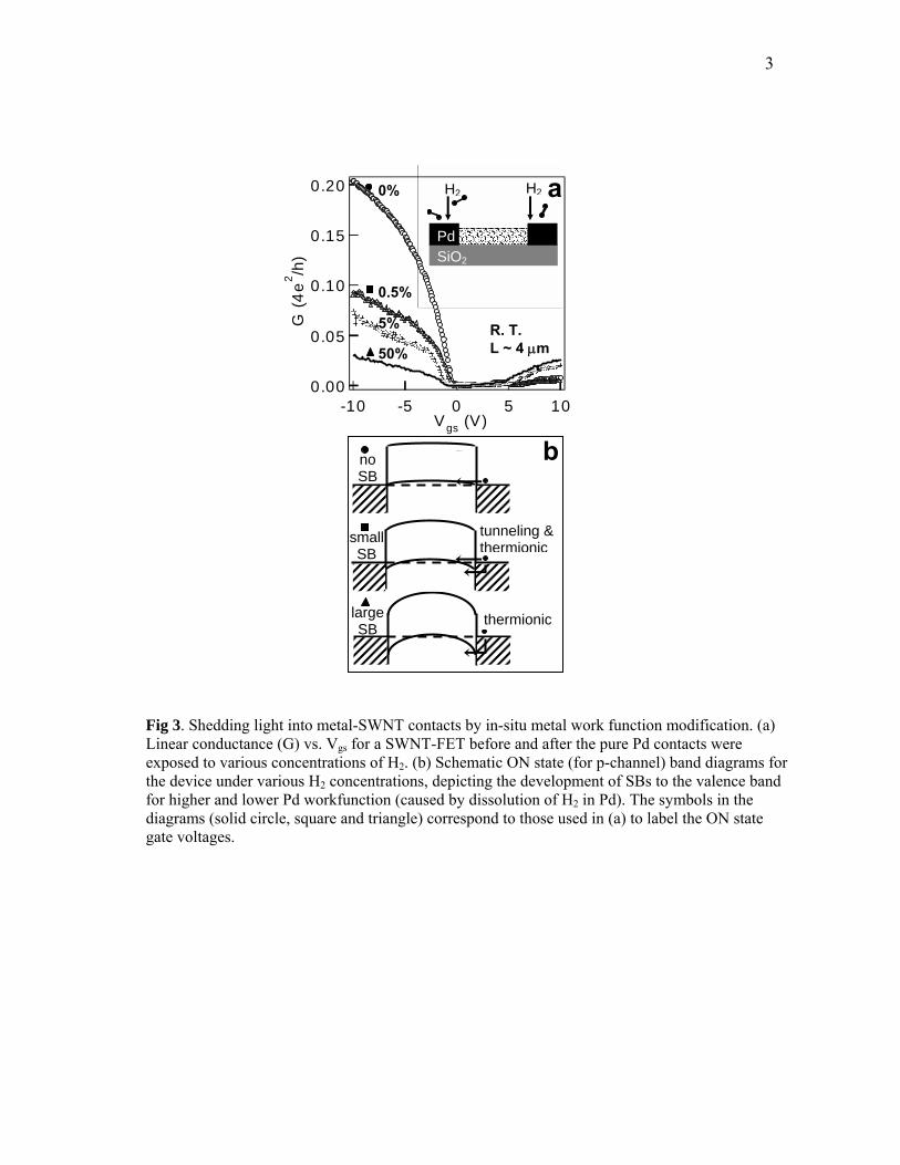
It is well established that the surface work function of Pd can be reversibly modified upon exposure to molecular hydrogen. Hydrogen molecules dissociate at the surface of Pd, resulting in atomic hydrogen that can dissolve in Pd and lower its work function. This phenomenon has been utilized to modify the metal contact work function of nanotube FETs in-situ and shed light on the SB height nature at the interfaces.5 Figure 3 shows the transfer characteristics of a Pd contacted nanotube device upon exposure to various concentrations of H2 in dry air. It is evident that as the concentration of H2 is increased and therefore the Pd work function is decreased, the p-channel (n-channel) conductance decreases (increases) due to the Schottky barrier height modulation at the Pd-nanotube interfaces (Fig.3). This result provide a clear experimental proof of the lack of Fermi level pinning at the interfaces and demonstrates the large sensitivity of Schottky barrier height on the work function of the metal contacts. Metal Type and Diameter Dependence of Electrical Contacts to Carbon Nanotubes
Recently, we have found that Rh can afford similar contact interfaces to nanotubes as Pd.17 While
Electrical Transport Properties and Field-Effect Transistors of Carbon Nanotubes
3 near-zero SB contacts can be made to d > ~1.6 nm semiconducting nanotubes with Pd or Rh metal contacts, non-negligible positive SBs exist for smaller diameter nanotubes due to their larger band gap (Fig 4). Metal type and diameter dependent contacts to semiconducting SWNTs have also been investigated by Chen et al.18 Beside the Schottky barriers, pure tunneling barriers (gate independent) may also develop at the metal-nanotube interface, therefore, limiting the ON-state conductance and current drive of a device. These pure tunneling barriers can be observed when metal-nanotube bonding interactions are weak and the relaxation bond lengths are large. As a result, charge carriers have to tunnel through a “vacuum” interface between the metal and nanotube. Experimental observations have shown that Pd and Rh are favorable as contact materials over other high work function metals such as Au and Pt. This may in fact be due to the larger bonding interactions between Pd/Rh and nanotube as compared to Pt and Au, although more detailed experimental and theoretical work is still needed to better understand the precise nature of this observation.
A surprising observation is that the contact resistance between Pd/Rh electrodes and metallic nanotubes is also found to be diameter dependent for small nanotubes (Fig. 4).17 Since there are no SBs at the interface for zero band gap metallic nanotubes, the low current drive for d ≤ ~ 1.0 nm nanotubes is attributed to the development of pure tunneling barriers as the chemical reactivity of nanotubes is known to be diameter dependent. The existence of SBs for small semiconducting SWNTs is responsible for lower currents than in same-diameter metallic tubes. Chemical doping can be invoked to suppress the positive SBs as demonstrated experimentally.19 However, the tunnel barrier appears to be independent of doping and causes non-ohmic contact for d < 1.2nm SWNTs (for semiconducting and metallic tubes alike) even under chemical doping. Little is known currently about how to suppress this contact barrier for such small diameter SWNTs. The origin of this tunnel barrier could be coming from significant alteration of the SWNT structure due to chemical perturbations by the contact metal. That is, small nanotubes are chemically more reactive than larger tubes, and the interaction with metal atoms may give rise to invasive contact effects that lead to degradation of the transport properties of the nanotubes at the electrodes. This possibility however, requires further investigation.
Making ohmic contacts to very small (d ≤ 1 nm) nanotubes is currently a key challenge and requires developing a strategy to eliminate the large electrode tunnel barriers. Various chemical synthesis methods including HiPco20 and CoMo21 are known to produce very small tubes predominantly in the 0.7-1.2 nm range. An ohmic contact solution for down to 0.7 nm tubes will be needed in order to enable high performance electronics with these materials. To achieve this goal, systematic experiments and
theoretical understanding will be needed, including continued search for an optimum contact metal. High-κ Dielectric Integration
Thin films of high-κ materials, such as ZrO2 and HfO2 (κ~15-25), are highly desirable for gate dielectric integration in field-effect transistors as they enable high ON-state current densities (speed) and low operating power consumptions. The integration of high-κ dielectrics, however, has been a challenge in planar MOSFETs because of the inherent mobility degradation of the Si channels. A unique advantage of carbon nanotubes is their compatibility with high-κ dielectrics. The lack of dangling bonds at the nanotube/high-κ interface and the weak non-covalent bonding interactions between the two materials, prevent any perturbation of electron transport in carbon nanotubes.4
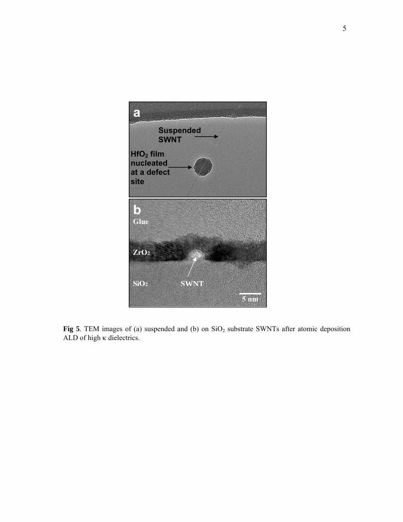
Figure 5 shows TEM images of suspended (a) and on substrate (b) carbon nanotubes after atomic layer deposition (ALD) of ~ 8 nm thick high-κ film. It is evident that high-κ materials do not nucleate on pristine carbon nanotubes,6 except at defect sites (Fig. 5a). For nanotube devices on substrates, the ALD of high-κ dielectrics initiates on the surrounding SiO2 substrate and “drowns” the nanotubes once the thickness of the film surpasses the diameter of the nanotube (Fig. 5b). As a result, the interface bonding between nanotubes and the high-κ dielectric is only through weak van der Waals forces, and the intrinsic chemical and physical nature of the nanotubes are well preserved after ALD. However, since as-grown SWNT-derived FETs with high-κ dielectrics rely on ALD nucleation and growth on OH-terminated SiO2 substrates, ALD of relatively thick high-κ films (≥ 8nm) are needed to fully cover the SWNTs and avoid gate leakage.
Recently, we found that by non-covalent functionalization of SWNTs with ploy-T DNA molecules (dT40), one can impart functional groups of sufficient density and stability for uniform and conformal ALD of high-κ dielectrics with thickness down to 2-3 nm on SWNTs (Fig. 6).22 This enables us to approach the ultimate vertical scaling limit of nanotube FETs and reliably achieve S ~ 60 mV/decade at room temperature (Fig. 7). For nanotube FETs without DNA functionalization, severe gate leakage and shorts were observed for most FETs with high-κ thickness tox ≤ 5nm. With DNA functionalization, high performance nanotube/high-κ FETs were reliably obtained with HfO2 down to tox ~ 2 nm (Fig.7). These DNA functionalized SWNT FETs reproducibly reached the theoretical limit of S ~ 60 mV/decade at 300 K (Fig. 7a).22 With non-covalent DNA functionalization, we observed no degradation in the SWNT FET conductance after the functionalization and subsequent ALD. We have carried out microscopy investigations to understand ALD processes on SWNTs with and without DNA functionalization (Fig. 6). For SWNTs

4 H. Dai
on SiO2 substrates with DNA functionalization, we observed concurrent ALD of HfO2 on both nanotube and SiO2 surfaces, evidenced by the post-ALD topographic height difference between the nanotube site and surrounding being approximately the tube diameter d (Fig. 6a left panel). In contrast, for SWNTs on SiO2 without DNA functionalization, ‘grooves’ were observed along the nanotubes after ALD of HfO2 (Fig. 6a right panel), indicating the lack of nucleation and growth of HfO2 directly on the tube surface and engulfing of the tube by HfO2 grown on the SiO2. We also carried out ALD on suspended SWNTs grown on transmission electron microscopy (TEM) grids. With DNA functionalization, suspended SWNTs allowed for quasi-continuous and conformal HfO2 coating by ALD (Fig. 6b left image). This differed from ‘balling up’ of high-κ material locally on as-grown tubes presumably on defect site (Fig. 6b right image).6,23
Our microscopy data provides direct evidence of active nucleation and growth of HfO2 on the sidewalls of DNA functionalized SWNTs in ALD. DNA is known to non-covalently absorb24 on SWNT sidewalls via π-stacking25 of the base-pairs. Such functionalization is found to be thermally stable at the ALD temperature of 90 ºC. The functional groups in DNA molecules (OH, phosphate, etc) are involved in chemisorption of precursor species in the ALD process, affording uniform nucleation and growth of HfO2 coating on nanotubes.
The vertical scaling of high-κ dielectrics for SWNT FETs is expected to be useful for investigating interesting device physics in quasi-1D systems such as electron tunneling. In a 1D channel, electrostatics are dependent on the gate dielectric thickness and the widths of tunnel barriers (Schottky, band-to-band tunneling BTBT,26,27 etc) are often set by the gate dielectrics thickness.28 Approaching the Performance Limit – Nearly Ballistic Nanotube FETs To explore the potential of nanotube building blocks for nanoelectronic applications, it is essential to explore their performance limit and compare it with the state-of-the-art silicon technology. In order to approach the performance limit, it is desirable to integrate high-κ gate dielectrics, zero barrier contacts, ballistic nanotube channels, and self-aligned fabrication strategies for the ideal alignment of the gate with respect to the S/D. The first two criteria were discussed earlier. Ballistic transport can be observed in nanotube channels at sub-100 nm length scales as the electron scattering mean free path (mfp) with acoustic phonons lac ~ 1 μm, with defects ldef ~ 1μm, and with optical phonons lop ~ 15 nm.29 30 31 Although optical phonons have a relatively short mean free path, these high energy phonon modes (~ 0.2 eV) do not play a significant scattering role at low VDS.32 As a result,
quasi ballistic transport can be readily observed in nanotubes at relatively long lengths owing to the large mfp of the defects and acoustic phonons.
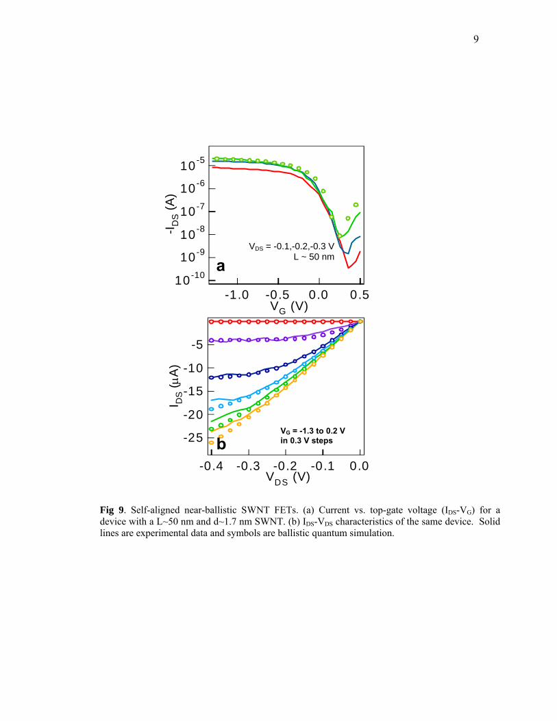
We have developed a novel strategy that combines all of the mentioned criteria for approaching the performance limit (Fig 8 and 9) of nanotube FETs. The gate stack acts as a mask in forming the “self-aligned” Pd S/D electrodes as described in Ref. 6. This approach allows the fabrication of nanotube FETs with no significant overlap or underlap of the gate with the S/D electrodes (Fig. 8a), minimizing the parasitic capacitance and resistance of the structures.
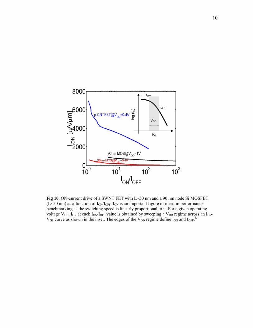
The electrical transport properties of a miniaturized self-aligned SWNT-FET with high-κ gate dielectric and L ~ 50 nm is shown in Fig. 9, exhibiting high peak transconductance of ~ 30 μS, maximum linear ON-state conductance of ~ 0.5×4e2/h and saturation current up to ~25 μA for a d ~ 1.7 nm tube.6 The experimental data (solid lines, Fig. 9) is consistent with the simulation (symbols, Fig. 9) which assumes ballistic transport in the channel. This suggests that the nanotube FET with integrated high-κ gate dielectric is operating near the ballistic regime with no extra sources of resistance in the channel or at the interface. As a result, the device is capable of delivering high currents at low VDS, which is significant for realizing fast and low power electronics. To compare the performance of this SWNT FET with the state-of-the-art Si MOSFETs, the current densities of the two technologies are evaluated as a function of ION/IOFF in Fig. 10.33 For all ION/IOFF values, the SWNT FET outperforms the Si MOSFET at the same VDD. By developing better contact technologies to smaller diameter tubes, it should be possible to achieve even higher ION/IOFF while maintaining the same ION, by using larger band gap nanotubes. Novel device concepts, such as chemically doped S/D SWNT FETs19 and band-to-band tunneling FETs27,34 have also been shown to be promising in further improving the ION/IOFF by reducing the OFF-state leakage currents. High-Field Transport Properties: Nanotubes on Substrates.
High-field transport properties of SWNTs are important to high power operations of nanotube electronics. Despite the ballistic nature of transport in SWNTs at low bias (where the intrinsic resistance is close to h/4e2 ≈ 6.5 kΩ), strong electron-optical phonon (OP) scattering dominates high-field transport, when electrons can gain energies more than 0.16 eV, the zone-boundary OP energy.29 In general, the electron-acoustic phonon (AP) interaction in SWNTs is assumed to be nearly elastic (electrons are simply backscattered, but their energy is not changed) while the OP interaction is strongly inelastic, such that electrons lose (gain) ħωOP ≈ 0.16-0.20 eV energy when emitting (absorbing) OP phonons.29 These effects are gleaned from transport data of ohmically contacted metallic SWNTs in the low and high-bias regimes as a function of tube lengths (Fig. 11a). At high biases,
Electrical Transport Properties and Field-Effect Transistors of Carbon Nanotubes
5 currents saturate at the ~20 μA level for long tubes due to the optical or zone-boundary phonon scattering, but the currents increase for shorter tubes (Fig. 11b). Monte Carlo simulations of the electrical characteristics are carried out to solve the Boltzmann transport equation. Fitting the calculated current vs. bias voltage curves (Fig. 11b symbols) to the experimental results (Fig. 11b lines) reveals a mean free path (mfp) of lap ~ 300 nm for acoustic phonon backscattering and a mfp of lop ~ 15 nm for optical phonon backscattering. By reducing the nanotube length to ~10-15nm, up to 110 μA of current can be delivered through an ultra-short SWNT,35 corresponding to ~ 4×10⁹ A/cm2 current density (or 55,000 A/m, normalized by nanotube diameter). This current density is three orders of magnitude higher than that tolerable by a typical metal (e.g. Cu or Al) before breakdown via electromigration. Carbon nanotubes can sustain such high currents due to the strong chemical bonding in the covalent sp2 carbon network.
Recent work has shown that metallic SWNTs on insulating substrates (e.g. SiO2, Si3N4) heat up significantly at very high-biases, suggesting that the experimentally observed current saturation (around 20 µA for tubes longer than 1 µm) may be limited by Joule self-heating.36 37 Researchers have been able to reproduce on-substrate current-voltage (I-V) characteristics by including a simple Joule heating model, without the assumption of phonon non-equilibrium,36 37 although some arguments to the contrary also exist.38 The presence of non-equilibrium hot phonons in tubes on solid substrates is less certain than for suspended SWNTs (see section below), since hot OP phonons may couple with and decay into the substrate modes. Figure 12 shows the electrical characteristics of a 3 µm long metallic SWNT on a SiO2 substrate, up to breakdown in air near 15 V. Since breakdown in inert (e.g. Ar) gas ambients occurs at much higher voltages, the breakdown in air is attributed to burning by oxidation, which occurs when the peak temperature of the tube reaches about 600 oC = 873 K.39 The inset of Fig. 12 shows the experimental40 trend (squares) of breakdown voltages for metallic SWNTs, which scales approximately as 5 V/µm with the nanotube length for tubes longer than 1 µm. This implies a breakdown voltage around 15 V for a 3 µm long metallic SWNT, as seen in the experimental I-V curve. The scaling of breakdown voltage with length can be used to assess the SWNT-to-substrate thermal conductance, which is approximately 0.17 WK-1m-1 per nanotube length. This value is up to an order of magnitude lower than the thermal conductance due to the substrate itself, suggesting that heat loss from the metallic SWNT is limited by the nanotube-substrate interface rather than the thermal properties of the substrate.
In metallic SWNTs shorter than about 1 µm, the high-bias current has been experimentally observed to be notably higher than 20 µA (Fig. 11b).
Recent analysis suggests this current enhancement is aided by increased heat dissipation and sinking at the contacts,36 37 rather than along the length of the tube itself. The nature of the contacts and of the contact resistance (both electrical and thermal) play more significant role for such short tubes, in the length range comparable to or shorter than both the electron and the phonon mean free paths. Undoubtedly, more research needs to be done to understand the nature of high-field transport and power dissipation in very short SWNTs. However, with advances in understanding both electrical and thermal transport in SWNTs, engineering solutions may eventually be found to optimize both types of transport, and consequently yield more reliable and efficient carbon nanotubes for device and interconnect applications. High Field Transport Properties: Suspended Nanotubes. Despite their very high thermal conductivity, the thermal conductance of SWNTs is relatively low, owing to their small diameter.41 The consequences of this low conductance are most evident in the electrical characteristics at high-bias in freely suspended SWNTs, as shown in Fig. 13. While even long SWNTs on insulating substrates exhibit very high (~20 μA) currents at high bias, recent work has shown that suspended nanotubes carry high-bias currents almost an order of magnitude lower (Fig.13), due to significant self-heating and electron scattering with hot non-equilibrium phonons.42 This observation is consistent with other recent studies indicating much longer phonon lifetimes in suspended SWNTs.43 The lack of an intimate coupling with a solid substrate has a two-fold effect on the high-bias electrical characteristics of a suspended nanotube: (1) it restricts the dissipation of Joule heat along the SWNT, facing a much higher thermal resistance (due to the small diameter) and leading to significant temperature rise, and (2) it removes direct phonon relaxation channels into the substrate, preventing the immediate decay of the generated SWNT OPs and significantly raising their population (beyond the thermal average). Mann et al. have shown that even gaseous “substrates” in contact with suspended SWNTs can reduce hot OP lifetimes, by introducing additional phonon decay channels.44 The suspended SWNTs in gas ambients deliver high-bias currents larger than those in vacuum, but lower than for similar SWNTs on solid substrates.44
As a consequence, freely suspended, unperturbed SWNTs in vacuum seem to represent the extreme case of a thermally isolated and long phonon lifetime scenario for nanotubes. All such suspended SWNTs exhibit negative differential conductance (NDC) (Fig. 13b), but the longer ones (10 μm) show it at much lower electric fields (~200 V/cm) than predicted by theoretical models that assume isothermal conditions (~5 kV/cm).45 This also indicates that the observed NDC is a thermal and not electrical (e.g.

6 H. Dai
contact or field-related) effect. A simple two-temperature (corresponding to acoustic and optical phonons) model42 can be used to calculate the theoretical I-V characteristics (solid lines in Fig. 13b). The optical phonons are assumed to be stationary with small group velocity, and the acoustic phonons are solely responsible for heat dissipation. The approach self-consistently computes the nanotube resistance, Joule heating and temperature along its length. A key feature is the temperature dependence of the SWNT thermal conductivity, which is found to be essential for reproducing the high bias behavior of the electrical characteristics. The approximately 1/V shape of the suspended SWNT I-V characteristics at high bias was found to be a consequence of the 1/T dependence of the thermal conductivity at high temperature from Umklapp-limited phonon scattering.42 This provides an indirect way to measure the thermal conductivity of individual suspended SWNTs in the high temperature regime,41 indicating it to be approximately described by 3600(300/T) Wm-1K-1 from 400 < T < 700 K. A more detailed study of the thermal conductance of individual SWNTs is described in Ref. 41.
The results above have implications to the application of nanotubes as interconnects and FETs, both of which will involve high current operation. It is interesting to note that self-heating effects in SWNT electronics including FETs (and optoelectronic devices) have been completely neglected thus far, partly owing to the quasi-ballistic transport in length scaled nanotube devices. Nevertheless, even for the shortest nanotube FETs (tens of nanometers) thus far, transport at high fields is still only quasi-ballistic with appreciable OP emission. Devising strategies to maximize OP decay in SWNT FETs could lead to further device performance and increase ON currents. Interface design for thermal management of SWNT electronics could therefore be an interesting direction for future research. Conclusions and Future Challenges
In conclusion, SWNTs are proven to be promising building blocks for future electronics. Due to their unique crystalline 1D structure, they are capable of delivering near-ballistic currents at relatively long channel lengths and are compatible with high-κ gate dielectrics. Much progress has been achieved in enabling ohmic contacts with zero Schottky barriers to SWNTs with diameters ≥ 1.5nm. However, transparent contacts to both metallic and semiconducting SWNTs with diameters on the order of 1 nm have not been achieved thus far. The 1-1.3 nm diameter range is important since SWNTs synthesized by many growth techniques fall into this range. The lack of ohmic contacts to SWNTs in this range may limit the applications of these materials for high performance electronics. Dielectric integration into carbon nanotube FETs has enabled vertical scaling to the 2 nm regime as facilitated by non-covalent chemical functionalization. High quality gate stacks for SWNT FETs can be easily obtained owing
to advances in high-κ integration and the lack of dangling bonds and interface states on nanotube surfaces. In order to obtain high current nanotube FETs to compete with planar silicon transistors, one must pack SWNTs at a pitch of about twice the diameter of nanotubes, wire up these nanotubes in parallel and use them as transistor channels collectively. Importantly, only semiconducting nanotubes should be included in such FET devices to avoid electrical shorts. These are currently the most formidable challenges to the carbon nanotube electronics area. Much work is required in order to pack and assemble nanotubes together in controlled fashions, and importantly, be able to do so with only semiconducting nanotubes (or metallic tubes for other applications).
Electrical Transport Properties and Field-Effect Transistors of Carbon Nanotubes
7 References 1. Dekker, C. Carbon nanotubes as molecular
quantum wires. Phys. Today 52, 22-28. (1999).
2. McEuen, P. L., Fuhrer, M. S. & Park, H. K. Single-walled carbon nanotube electronics. IEEE Trans. Nanotechnology 1, 78-85 (2003).
3. Dai, H. Carbon nanotubes: opportunities and challenges. Surf. Sci. 500, 218-241 (2002).
4. Javey, A. et al. High-k dielectrics for advanced carbon-nanotube transistors and logic gates. Nature Materials 1, 241 - 246 (2002).
5. Javey, A., Guo, J., Wang, Q., Lundstrom, M. & Dai, H. J. Ballistic carbon nanotube field-effect transistors. Nature 424, 654-657 (2003).
6. Javey, A. et al. Self-Aligned Ballistic Molecular Transistors and Electrically Parallel Nanotube Arrays. Nano Lett. 4, 1319-1322 (2004).
7. Durkop, T., Getty, S. A., Cobas, E. & Fuhrer, M. S. Extraordinary mobility in semiconducting carbon nanotubes. Nano Lett. 4, 35-9 (2004).
8. Lin, Y. M. et al. High-performance dual-gate carbon nanotube FETs with 40-nm gate length. IEEE Elec. Dev. Lett. 26, 823-825 (2005).
9. Lundstrom, M. Moore's law forever? Science 299, 210-1 (2003).
10. Tans, S., Verschueren, A. & Dekker, C. Room-temperature transistor based on a single carbon nanotube. Nature 393, 49-52 (1998).
11. Martel, R., Schmidt, T., Shea, H. R., Hertel, T. & Avouris, P. Single- and multi-wall carbon nanotube field-effect transistors. Appl. Phys. Lett. 73, 2447-2449 (1998).
12. Soh, H. et al. Integrated nanotube circuits: controlled growth and ohmic contacting of single-walled carbon nanotubes. Appl. Phys. Lett. 75, 627-629 (1999).
13. Zhou, C., Kong, J. & Dai, H. Electrical measurements of individual semiconducting single-walled nanotubes of various diameters. Appl. Phys. Lett. 76, 1597 (1999).
14. Heinze, S. et al. Carbon nanotubes as Schottky barrier transistors. Phys. Rev. Lett. 89, 6801 (2002).
15. Tersoff, J. Schottky barrier heights and the continuum of gap states. Phys. Rev. Lett. 52, 465–468 (1984).
16. Leonard, F. & Tersoff, J. Role of Fermi-level pinning in nanotube Schottky diodes. Phys. Rev. Lett. 84, 4693-4696 (2000).
17. Kim, W. et al. Electrical contacts to carbon nanotubes down to 1 nm in diameter. Appl Phys Lett 87, 1-3 (2005).
18. Chen, Z. H., Appenzeller, J., Knoch, J., Lin, Y. M. & Avouris, P. The role of metal-nanotube contact in the performance of carbon
nanotube field-effect transistors. Nano Lett. 5, 1497-1502 (2005).
19. Javey, A. et al. High performance n-type carbon nanotube field-effect transistors with chemically doped contacts. Nano Lett. 5, 345-348 (2005).
20. Nikolaev, P. et al. Gas-phase catalytic growth of single-walled carbon nanotubes from carbon monoxide. Chem. Phys. Lett. 313, 91-97 (1999).
21. Kitiyanan, B., Alvarez, W. E., Harwell, J. H. & Resasco, D. E. Controlled production of single-wall carbon nanotubes by catalytic decomposition of CO on bimetallic Co-Mo catalysts. Chem. Phys. Lett. 317, 497-503 (2000).
22. Lu, Y. et al. DNA functionalization of carbon nanotubes for ultrathin atomic layer deposition of high kappa dielectrics for nanotube transistors with 60 mV/decade switching. J. Am. Chem. Soc. 128, 3518-3519 (2006).
23. Farmer, D. B. & Gordon, R. G. ALD of high-kapp dielectrics on suspended functionalized SWNTs. Electrochem. Sol.-State Lett. 8, G89-91 (2005).
24. Zheng, M. et al. DNA-assisted dispersion and separation of carbon nanotubes. Nature Materials 2, 338-342 (2003).
25. Chen, R., Zhang, Y., Wang, D. & Dai, H. Non-covalent sidewall functionalization of single-walled carbon nanotubes for protein immobiloization. J. Am. Chem. Soc. 123 (2001).
26. Zhou, C., Kong, J., Yenilmez, E. & Dai, H. Modulated chemical doping of individual carbon nanotubes. Science 290, 1552 (2000).
27. Appenzeller, J., Lin, Y. M., Knoch, J., Chen, Z. H. & Avouris, P. Comparing carbon nanotube transistors - the ideal choice: a novel tunneling device design. IEEE Trans. Elec. Dev. 52, 2568-76 (2005).
28. Guo, J., Wang, J., Polizzi, E., Datta, S. & Lundstrom, M. Electrostatics of nanowire transistors. IEEE Trans. Nanotech. 2, 329-334 (2003).
29. Yao, Z., Kane, C. L. & Dekker, C. High-field electrical transport in single-wall carbon nanotubes. Phys. Rev. Lett. 84, 2941-2944 (2000).
30. Javey, A. et al. High-Field, Quasi-Ballistic Transport in Short Carbon Nanotubes. Phys. Rev. Lett. 92, 106804 (2004).
31. Park, J.-Y. et al. Electron-Phonon Scattering in Metallic Single-Walled Carbon Nanotubes. Nano Lett. 4, 517 (2004).
32. Guo, J. & Lundstrom, M. Role of phonon scattering in carbon nanotube field-effect transistors. Appl. Phys. Lett. 86, 193103-05 (2005).

8 H. Dai
33. Guo, J., Javey, A., Dai, H. & Lundstrom, M. Performance analysis and design optimization of near ballistic carbon nanotube field-effect transistors. International Electron Devices Meeting, 703-6 (2004).
34. Appenzeller, J., Lin, Y.-M., Knoch, J. & Avouris, P. Band-to-Band Tunneling in Carbon Nanotube Field-Effect Transistors. Phys. Rev. Lett. 93, 2004 (2004).
35. Javey, A., Qi, P., Wang, Q. & Dai, H. Ten- to 50-nm-long quasi-ballistic carbon nanotube devices obtained without complex lithography. Proc. Nat.Acad. Sci. 101, 13408 (2004).
36. Pop, E., Mann, D., Reifenberg, J., Goodson, K. E. & Dai, H. IEDM Technical Digest., 253-6 (2005), Washington DC.
37. Kuroda, M. A., Cangellaris, A. & Leburton, J. P. Nonlinear transport and heat dissipation in metallic carbon nanotubes. Phys. Rev. Lett. 95, 266803-6 (2005).
38. Lazzeri, M., Piscanec, S., Mauri, F., Ferrari, A. C. & Robertson, J. Electron transport and hot phonons in carbon nanotubes. Phys. Rev. Lett. 95, 236802-05 (2005).
39. Chiang, I. W. et al. Purification and characterization of single-wall carbon nanotubes (SWNTs) obtained from the gas-phase decomposition of CO (HiPco process). J. Phys. Chem. 105, 8297-301 (2001).
40. Qi, P. F. et al. Miniature organic transistors with carbon nanotubes as quasi-one-dimensional electrodes. J. Am. Chem. Soc. 126, 11774-11775 (2004).
41. Pop, E., Mann, D., Wang, Q., Goodson, K. & Dai, H. Thermal conductance of an individual single-wall carbon nanotube above room temperature. Nano Lett. 6, 96-100 (2006).
42. Pop, E. et al. Negative differential conductance and hot phonons in suspended nanotube molecular wires. Phys. Rev. Lett. 95, 155505-08 (2005).
43. LeRoy, B. J., Lemay, S. G., Kong, J. & Dekker, C. Electrical generation and absorption of phonons in carbon nanotubes. Nature 432, 371-374 (2004).
44. Mann, D. et al. Thermally and molecularly stimulated relaxation of hot phonons in suspended carbon nanotubes. J. Phys. Chem. 110, 1502-1505 (2006).
45. Perebeinos, V., Tersoff, J. & Avouris, P. Electron-phonon interaction and transport in semiconducting carbon nanotubes. Phys. Rev. Lett. 94, 086802-05 (2005).

1
a
(10,10) armchair metallic
(11,7) chiral
semiconductor
(10,10)
a2
Rnm=(n,m)=(11,7)
a1
b c
Fig 1. Folding of graphene into nanotubes. (a) Various chiralities of carbon nanotubes can be obtained by folding along different wrapping vectors Rnm. (b) and (c) are schematics of (10,10) and (11,7) nanotubes. A (n,m) tube is metallic when n=m (armchair). A nanotube with n-m=3j, where j is an integer, is a semi-metal with a curvature-induced band gap on the order of few meV. A nanotube is semiconducting when n-m≠3j.

2
150 K
c50 K
280 K
-15 -7.76-7.65
15
Vgs (V)
Vds
(mV)
L = 0.3 μm
1 μm
0.4
0.2
a
0.0
G (4
e2 /h)
-10 0
c
10Vgs (V)
L = 0.3 μm d Vgs = -13 V
0.6
0.5
0.4
0.3
GO
N (4
e/h
)2
200100T (K)
~4e2/h D
S
D
Fig 2. Pd contacted and back-gated SWNT-FETs on Si/SiO2 (tox~500 nm) substrates. (a) Scanning electron microscopy (SEM, left) and atomic force microscope (AFM, right) images of a SWNT bridging three Pd contacts (b) Schematic view of a device. (c) Transconductance G vs. Vgs for a 300 nm long tube device at various temperatures. Differential conductance dIds/dVds vs. Vds and Vgs (inset) at T=1.5 K shows a Fabry-Perot like interference pattern, a hallmark of ballistic transport. (d) ON-state conductance as a function of temperature for the same device.
0.3 μm
3 μm
50 μm
(Pd)
(Pd)
(Pd)
D
D
S
a
d
SiO2
p+ Si (gate)
S (Pd) D (Pd)
b
3
H2
Pd SiO2
H2 a 0%
0.5%
5%
50% R. T. L ~ 4 μm
no SB
large SB
small SB
b
tunneling & thermionic
thermionic
Fig 3. Shedding light into metal-SWNT contacts by in-situ metal work function modification. (a) Linear conductance (G) vs. Vgs for a SWNT-FET before and after the pure Pd contacts were exposed to various concentrations of H2. (b) Schematic ON state (for p-channel) band diagrams for the device under various H2 concentrations, depicting the development of SBs to the valence band for higher and lower Pd workfunction (caused by dissolution of H2 in Pd). The symbols in the diagrams (solid circle, square and triangle) correspond to those used in (a) to label the ON state gate voltages.
0.20
0.15
0.10
0.05
0.00
G (4
e2 /h)
-10 -5 0 5 10Vgs (V)

4
20
15
10
5
-I on
(μA
)
2.52.01.51.0d (nm)
Metallic Semiconducting
FIG. 4. Diameter dependent electrical properties of metallic and semiconducting SWNTs. Room
temperature Ion (defined as the current under |Vds| = 1V) vs. d plots for both metallic and semiconducting SWNT devices with Rh or Pd contact (similar results for both metals).
5
a
HfO2 film nucleated at a defect site
Suspended SWNT
b
SWNT
Fig 5. TEM images of (a) suspended and (b) on SiO2 substrate SWNTs after atomic deposition
ALD of high κ dielectrics.

6
HfO2
~d
SWNT 200nm
SWNT 200nm
Fig. 6. ALD of HfO2 on SWNTs with and without DNA functionalization. (a) AFM images of ~ 5nm thick HfO2 coatings on SWNTs lying on SiO2 with (left image) and without (right side) DNA functionalization prior to ALD. Cross-sectional view schematics of the coating profiles are shown under images. (b) TEM images of nominally 5nm thick ALD-HfO2 coating on suspended SWNTs with (left) and without (right) DNA functionalization respectively. Note that the uniformity of high κ coatings on DNA-treated SWNTs is imperfect, but are drastically better than those on non-functionalized nanotube.
10 nm 0
10nm 20nm
(b)
(a)
with DNA no DNA
SiO2
SWNT with DNA
DNA coating
SiO2
HfO2
SWNT, no DNA
HfO2

7
60 mV/dec
a
10-14
10-12
10-10
10-8
10-6
| Ids
(A) |
0.60.40.20.0-0.2-0.4Vg (V)
- 0.6V - 0.3V - 0.1V - 0.01V
-4
-3
-2
-1
I ds (x
10-6
A)
-1.0 -0.8 -0.6 -0.4 -0.2
0.1V
- 0.0Vb
- 0.1V
- 0.2V
- 0.3V
- 0.4V
- 0.5V
0.0Vds (V)
Fig. 7. A DNA-functionalized SWNT-FET (d~1.2nm) with tox~2nm high κ gate dielectrics. (a) Current vs. top-gate voltage characteristics. (b) Current vs bias-voltage characteristics under various gate voltages labeled on each curve.

8
Al
G
HfO2
10 nm SiO2
p++ Si
S D
D S G
SWNT 100 nm
a
b
Fig 8. Self-aligned near-ballistic SWNT FETs. (a) Side-view schematic of a device. (b)Scanning electron microscopy (SEM) image showing the top-view of a device. The nanotube appears faint under the thin Pd electrodes.
9
VDS = -0.1,-0.2,-0.3 V L ~ 50 nm
a
-25
-20
-15
-10
-5
I DS (μ
A)
-0 .4 -0.3 -0.2 -0.1 0.0VDS (V)
10-10
10-9
10-8
10-7
10-6
10-5-I D
S (A
)
-1.0 -0.5 0.0 0.5VG (V)
b VG = -1.3 to 0.2 V in 0.3 V steps
Fig 9. Self-aligned near-ballistic SWNT FETs. (a) Current vs. top-gate voltage (IDS-VG) for a
device with a L~50 nm and d~1.7 nm SWNT. (b) IDS-VDS characteristics of the same device. Solid lines are experimental data and symbols are ballistic quantum simulation.
10
log
(I D)
VG
ION
IOFF
VDD
Fig 10. ON-current drive of a SWNT FET with L~50 nm and a 90 nm node Si MOSFET (L~50 nm) as a function of ION/IOFF. ION is an important figure of merit in performance benchmarking as the switching speed is linearly proportional to it. For a given operating voltage VDD, ION at each ION/IOFF value is obtained by sweeping a VDD regime across an IDS-VGS curve as shown in the inset. The edges of the VDD regime define ION and IOFF.33

11
L=600 nm 80 nm 40 nm 120 nm 10 nm
a
55 nm
85 nm
150 nm 300 nm
700 nm
60
40
20
0
I DS (μ
A)
1.51.00.5
b
0.0VDS (V)
Fig. 11. Length dependent electrical transport properties of SWNTs. (a) Atomic force microscopy (AFM) images of five devices consisting of individual SWNTs with lengths in the range of L=600 to 10 nm between the edges of Pd contact electrodes. (b) Electrical properties of ohmically contacted metallic SWNTs of various lengths. Solid lines are experimental current vs. bias curves and the symbols are Monte Carlo calculation and fitting results.

12
0 5 10 150
5
10
15
20
V (V)
I (μA
)
0 1 2 3 4 50
5
10
15
20
25
L (μm)
VB
D (
V)
VBD
Data
Linear Fit
L (μm)0 1 2 3 4 5
V BD
(V)
510152025
0
0 5 10 150
5
10
15
20
V (V)
I (μA
)
0 1 2 3 4 50
5
10
15
20
25
L (μm)
VB
D (
V)
VBD
Data
Linear Fit
L (μm)0 1 2 3 4 5
V BD
(V)
510152025
0
Fig. 12 Length dependent electrical breakdown of SWNTs on substrate. Measured electrical
I-V up to breakdown in air for a 3 μm long metallic SWNT (symbols, from Ref. 30 and simulation using the model of Ref. 36 (solid line). The simulation is interrupted when the peak temperature of the tube (in its middle) reaches TBD = 873 K. The inset shows the linear scaling of breakdown voltage with metallic SWNT length, at approximately 5 V/µm.

13
(a)
(a)
Fig. 13. Self heating and negative differential conductance of suspended SWNTs. (a) SEM (top) and diagram (bottom) of a metallic SWNT with one portion grown across a substrate, the other suspended across a trench. (b) The measured (symbols) and calculated (lines) I-V characteristics of the two nanotube segments in vacuum are plotted for a similar device with length 3 μm and diameter 2.4 nm.
0 0.2 0.4 0.6 0.8 1 1.20
2
4
6
8
10
12
14
16
I (μA
)
V (V)
On Substrate
Suspended
L = 3 μm
SiO2 Si3N4
nanotube Pt
Pt gate
2 μmnanotube on substrate suspended
over trench
(b)