Embed Size (px)
Citation preview
1 APN-002815 Rev 01 © 2021 Luminus Devices, Inc. - All Rights Reserved
Application Note
Electrical Stress Damage to LEDs and How to Prevent It
Table of Contents
1. Overview 2
2. Types & Root Causes of Electrical Stress Damage 3
3. Understanding EOS and ESD Models 5
4. Preventing Electrical Stress Damage: Handling Best Practices 9
5. Resources 11
6. References Cited 11
7. Contact (Customer Support) 11
Introduction
There are three major causes of LED performance degradation: contamination stress, thermal stress, and electrical stress. This application note addresses electrical stress factors including electrical overstress (EOS), electrostatic discharge (ESD), and reverse polarization. This application note summarizes the main points of prevention, troubleshooting, and remedying electrical stress damage in Luminus LED components. Luminus highly recommends that users reference and understand industry standards in conjunction with these
recommendations.
2 APN-002815 Rev 01 © 2021 Luminus Devices, Inc. - All Rights Reserved
Application Note
1. Overview
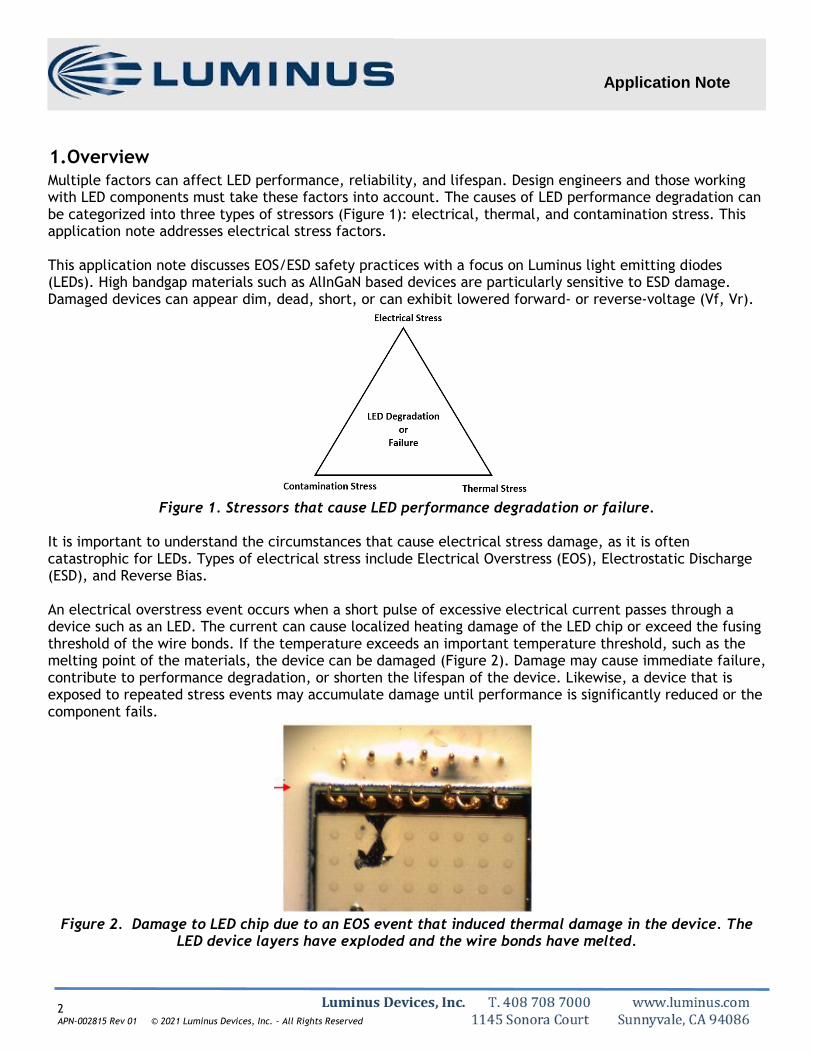
Multiple factors can affect LED performance, reliability, and lifespan. Design engineers and those working with LED components must take these factors into account. The causes of LED performance degradation can be categorized into three types of stressors (Figure 1): electrical, thermal, and contamination stress. This application note addresses electrical stress factors. This application note discusses EOS/ESD safety practices with a focus on Luminus light emitting diodes (LEDs). High bandgap materials such as AlInGaN based devices are particularly sensitive to ESD damage. Damaged devices can appear dim, dead, short, or can exhibit lowered forward- or reverse-voltage (Vf, Vr).
Figure 1. Stressors that cause LED performance degradation or failure.
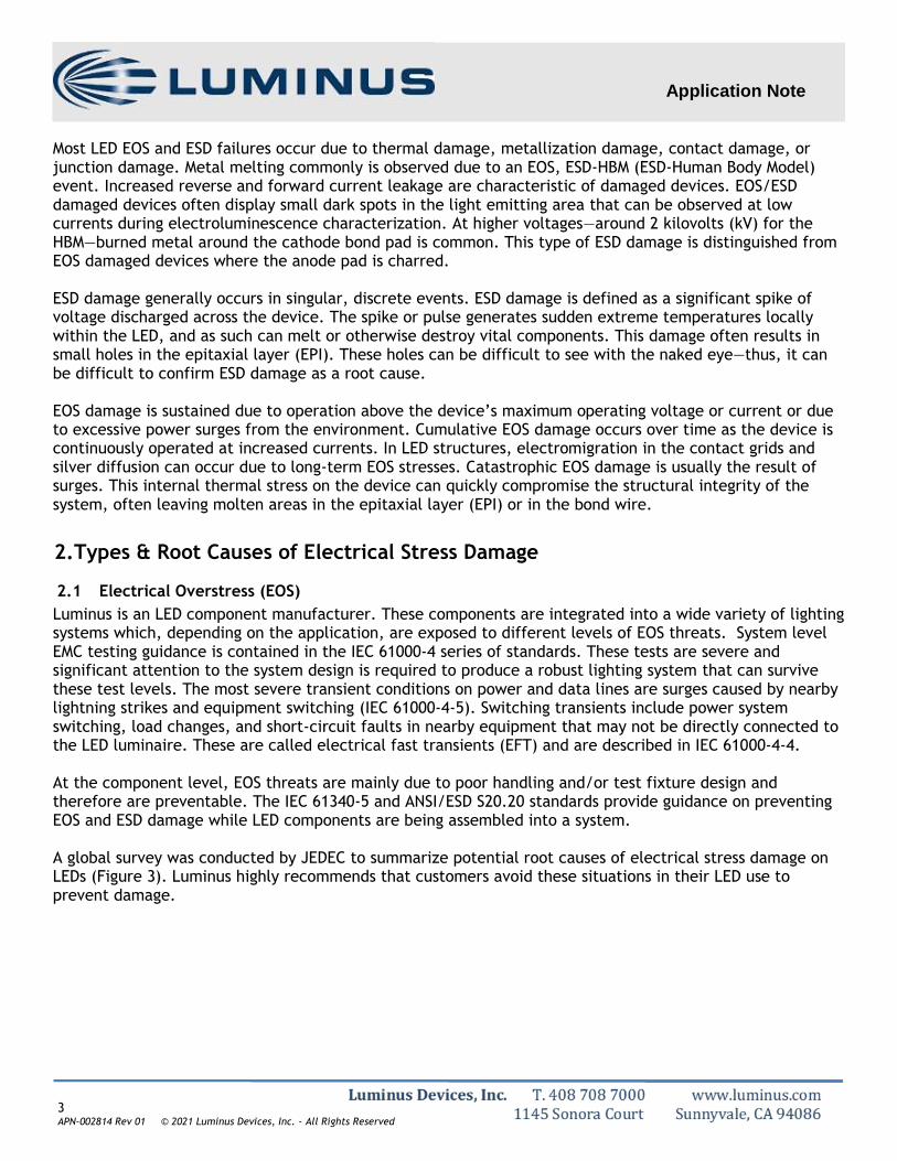
It is important to understand the circumstances that cause electrical stress damage, as it is often catastrophic for LEDs. Types of electrical stress include Electrical Overstress (EOS), Electrostatic Discharge (ESD), and Reverse Bias. An electrical overstress event occurs when a short pulse of excessive electrical current passes through a device such as an LED. The current can cause localized heating damage of the LED chip or exceed the fusing threshold of the wire bonds. If the temperature exceeds an important temperature threshold, such as the melting point of the materials, the device can be damaged (Figure 2). Damage may cause immediate failure, contribute to performance degradation, or shorten the lifespan of the device. Likewise, a device that is exposed to repeated stress events may accumulate damage until performance is significantly reduced or the component fails.
Figure 2. Damage to LED chip due to an EOS event that induced thermal damage in the device. The
LED device layers have exploded and the wire bonds have melted.
3 APN-002814 Rev 01 © 2021 Luminus Devices, Inc. - All Rights Reserved
Application Note
Most LED EOS and ESD failures occur due to thermal damage, metallization damage, contact damage, or junction damage. Metal melting commonly is observed due to an EOS, ESD-HBM (ESD-Human Body Model) event. Increased reverse and forward current leakage are characteristic of damaged devices. EOS/ESD damaged devices often display small dark spots in the light emitting area that can be observed at low currents during electroluminescence characterization. At higher voltages—around 2 kilovolts (kV) for the HBM—burned metal around the cathode bond pad is common. This type of ESD damage is distinguished from EOS damaged devices where the anode pad is charred. ESD damage generally occurs in singular, discrete events. ESD damage is defined as a significant spike of voltage discharged across the device. The spike or pulse generates sudden extreme temperatures locally within the LED, and as such can melt or otherwise destroy vital components. This damage often results in small holes in the epitaxial layer (EPI). These holes can be difficult to see with the naked eye—thus, it can be difficult to confirm ESD damage as a root cause. EOS damage is sustained due to operation above the device’s maximum operating voltage or current or due to excessive power surges from the environment. Cumulative EOS damage occurs over time as the device is continuously operated at increased currents. In LED structures, electromigration in the contact grids and silver diffusion can occur due to long-term EOS stresses. Catastrophic EOS damage is usually the result of surges. This internal thermal stress on the device can quickly compromise the structural integrity of the system, often leaving molten areas in the epitaxial layer (EPI) or in the bond wire.
2. Types & Root Causes of Electrical Stress Damage
2.1 Electrical Overstress (EOS)
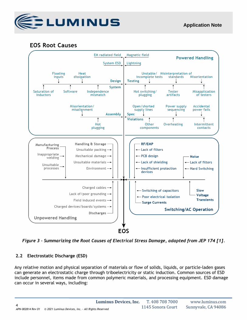
Luminus is an LED component manufacturer. These components are integrated into a wide variety of lighting systems which, depending on the application, are exposed to different levels of EOS threats. System level EMC testing guidance is contained in the IEC 61000-4 series of standards. These tests are severe and significant attention to the system design is required to produce a robust lighting system that can survive these test levels. The most severe transient conditions on power and data lines are surges caused by nearby lightning strikes and equipment switching (IEC 61000-4-5). Switching transients include power system switching, load changes, and short-circuit faults in nearby equipment that may not be directly connected to the LED luminaire. These are called electrical fast transients (EFT) and are described in IEC 61000-4-4. At the component level, EOS threats are mainly due to poor handling and/or test fixture design and therefore are preventable. The IEC 61340-5 and ANSI/ESD S20.20 standards provide guidance on preventing EOS and ESD damage while LED components are being assembled into a system. A global survey was conducted by JEDEC to summarize potential root causes of electrical stress damage on LEDs (Figure 3). Luminus highly recommends that customers avoid these situations in their LED use to prevent damage.
4 APN-002814 Rev 01 © 2021 Luminus Devices, Inc. - All Rights Reserved
Application Note
Figure 3 – Summarizing the Root Causes of Electrical Stress Damage, adapted from JEP 174 [1].
2.2 Electrostatic Discharge (ESD)
Any relative motion and physical separation of materials or flow of solids, liquids, or particle-laden gases can generate an electrostatic charge through triboelectricity or static induction. Common sources of ESD include personnel, items made from common polymeric materials, and processing equipment. ESD damage can occur in several ways, including:
5 APN-002814 Rev 01 © 2021 Luminus Devices, Inc. - All Rights Reserved
Application Note
A charged object (including a person) contacting an ESD-sensitive (ESDS) item.
A charged ESDS device contacting ground or another conductive object at a different potential.
An ESDS device is grounded while exposed to an electrostatic field. ESD damage usually happens as discrete events that are random in time, position, and polarity. If a repetitive failure mode is observed that is non-random, ESD is unlikely as a root cause and other potential factors should be carefully considered. The best guidance on preventing and managing ESD is outlined in these standards: ANSI/ESD S20.20 and (particularly) ESD TR20.20. Luminus strongly recommends customers follow the ESD control programs outlined in these standards; key points are summarized in this application note for quick reference.
2.3 Reverse Polarization
LEDs produce light in forward bias and are not generally designed for reverse bias operation. LEDs consist of a p-n junction, and if a high voltage surge goes through the device in the reverse direction the junction can be destroyed due to excessive currents. For any Luminus LEDs, unless the product datasheet specifically states safe parameters for reverse bias operation, the designer should assume that reverse bias operation will cause cumulative damage to the LED and lower its rated lifetime. LEDs are much more sensitive to reverse bias events compared to forward bias events, which is why single polarity (rather than back-to-back) Zener diodes are often used for ESD mitigation.
3. Understanding EOS and ESD Models The primary models for characterizing the ESD threshold of an electrical component are the Human Body Model (HMB) and the Charged Device Model (CDM). The main system level EOS models are Pulse, Electrical Fast Transients (EFT), and ESD. There are two sets of ESD standard models, one for components and one for systems. The system model is much more severe than the component model.
3.1 The Component-Level Human Body Model (HBM)
The human body is an effective conductor of electricity; we generate static through many common activities such as those shown in Table 1. Static electricity generation is also significantly affected by the amount of humidity in the ambient air.
Table 1. Typical voltage levels generated by different activities/objects [2].
Means of Generation 10-25 % Relative Humidity 65 – 99 % Relative Humidity
Walking across a carpet 35,000V 1,500V
Walking across vinyl tile 12,000V 250V
Worker at a bench 6,000V 100V
Poly bag picked up from bench 20,000V 1,200V
Chair with urethane foam 18,000V 1,500V
The HMB model (ANSI/ESDA/JDEC JS-001) is a mathematical representation of what occurs when a charged person contacts an uncharged part or vice versa. The HBM representation is based on an equivalent circuit with a charged 100-pF (picofarad) capacitor in series with a 1500 Ω (ohm) resistor.
6 APN-002814 Rev 01 © 2021 Luminus Devices, Inc. - All Rights Reserved
Application Note
3.2 The Component-Level Charged Device Model (CDM)
The CDM is a mathematical representation of a differential charge event between a component and any non-human object charged by triboelectricity or static induction. With the increased use of automation in manufacturing, machines that develop static charges which are not properly grounded can induce charges in nearby devices, which eventually discharge on contact with a conductor. Contact resistances are typically low in these instances, thus large, extremely short, short-duration currents can occur, for example e.g., 10 Amps (A) for 1-2 nanoseconds (ns). CDM currents are higher than HBM currents because there is no current limiting resistor in the path to limit the discharge. Threshold voltages for CDM are lower than HBM due to these higher currents.
3.3 The Component-Level Machine Model (MM)
Another model (now discontinued in most standards) is the Machine Model (MM). The MM represents ESD discharge resulting from a differential charge event between a piece of machinery and an electrical component. MM is designed to simulate a machine discharging through a device to ground. The model is based on a 200-pF capacitor and a 0Ω resistor. An inductive value is not specified, however most ESD equipment manufacturers place a 450 nH (nanohenries) inductor in the charge path. The MM model is considered similar enough to the HBM model that passing the HBM test implies passing the MM test as well. The MM is no longer used. The technical justification is detailed in JEP172A.
3.4 IEC 61000-4-2 ESD (System Level)
The system level ESD test waveform combines CDM and HBM events. It has a fast rise time (1 ns) to a peak current then a fast drop to an HBM type of waveform (Figure 4). The peak of the CDM transient is 3.75 A/kV and the maximum of the HBM component is 2 A/kV. Air discharge level 1 tests are performed at 2 kV and level 4 tests at 15 kV.
3.5 IEC 61000-4-4 Electrical Fast Transients (EFT) (System Level)
Electrical Fast Transient (EFT)/Burst events occur on a de-energized power distribution system when an inductive load (such as a relay, switch contactor, or heavy-duty motor) generates a burst of narrow-frequency transients. These fast transients can also be produced by a utility provider swapping in our out their power factor correction equipment. Power line transients can also be caused when an AC power cord is plugged in while equipment is switched off or when circuit breakers or open or closed. The stress methodology to deal with EFT events is similar to IEC-6100-4-2:2008, except for the repetitive fast transient test. This test consists of bursts of multiple fast transients, coupled into the power supply, control, and signal ports of a piece of equipment. For these tests, the short rise time, repetition rate, and low energy of the transients are significant: test voltages of up to 4 kV (in + and – polarities) are applied to the A/C power leads and up to 2kV is applied to the I/O cables using a coupling clamp. Then test voltages of 5 kHz pulse repetition frequency are applied for 60 seconds to each power supply terminal, including protective earth and every terminal combination.
3.6 IEC 61000-4-5 Surge (System Level)
System Level Surge tests are done to ensure equipment meets requirements for immunity to unidirectional surges caused by over voltages from switching and lightning transients. A surge is applied to the power terminals of the system under test via a capacitive coupling network. The test waveform is a slow but extremely severe pulse.
7 APN-002814 Rev 01 © 2021 Luminus Devices, Inc. - All Rights Reserved
Application Note
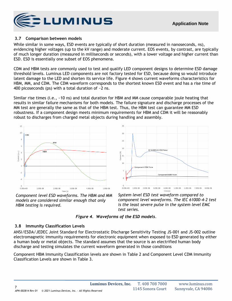
3.7 Comparison between models
While similar in some ways, ESD events are typically of short duration (measured in nanoseconds, ns), evidencing higher voltages (up to the kV range) and moderate current. EOS events, by contrast, are typically of much longer duration (measured in milliseconds or seconds), with a lower voltage and higher current than ESD. ESD is essentially one subset of EOS phenomena. CDM and HBM tests are commonly used to test and qualify LED component designs to determine ESD damage threshold levels. Luminus LED components are not factory tested for ESD, because doing so would introduce latent damage to the LED and shorten its service life. Figure 4 shows current waveforms characteristics for HBM, MM, and CDM. The CDM waveform corresponds to the shortest known ESD event and has a rise time of 400 picoseconds (ps) with a total duration of ~2 ns. Similar rise times (i.e., ~10 ns) and total duration for HBM and MM cause comparable joule heating that results in similar failure mechanisms for both models. The failure signature and discharge processes of the MM test are generally the same as that of the HBM test. Thus, the HBM test can guarantee MM ESD robustness. If a component design meets minimum requirements for HBM and CDM it will be reasonably robust to discharges from charged metal objects during handling and assembly.
Component level ESD waveforms. The HBM and MM models are considered similar enough that only HBM testing is required.
System level ESD test waveform compared to component level waveforms. The IEC 61000-4-2 test is the least severe pulse in the system level EMC test series.
Figure 4. Waveforms of the ESD models.
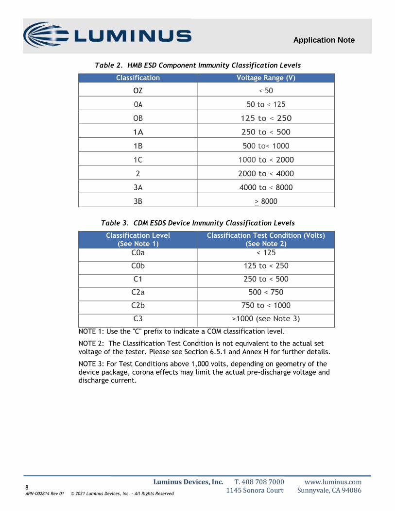
3.8 Immunity Classification Levels
ANSI/ESDA/JEDEC Joint Standard for Electrostatic Discharge Sensitivity Testing JS-001 and JS-002 outline electromagnetic immunity requirements for electronic equipment when exposed to ESD generated by either a human body or metal objects. The standard assumes that the source is an electrified human body discharge and testing simulates the current waveform generated in those conditions
Component HBM Immunity Classification levels are shown in Table 2 and Component Level CDM Immunity Classification Levels are shown in Table 3.
8 APN-002814 Rev 01 © 2021 Luminus Devices, Inc. - All Rights Reserved
Application Note
Table 2. HMB ESD Component Immunity Classification Levels
Classification Voltage Range (V)
OZ < 50
OA 50 to < 125
OB 125 to < 250
1A 250 to < 500
1B 500 to< 1000
1C 1000 to < 2000
2 2000 to < 4000
3A 4000 to < 8000
3B > 8000
Table 3. CDM ESDS Device Immunity Classification Levels
Classification Level (See Note 1)
Classification Test Condition (Volts) (See Note 2)
C0a < 125
C0b 125 to < 250
C1 250 to < 500
C2a 500 < 750
C2b 750 to < 1000
C3 >1000 (see Note 3)
NOTE 1: Use the "C" prefix to indicate a COM classification level.
NOTE 2: The Classification Test Condition is not equivalent to the actual set voltage of the tester. Please see Section 6.5.1 and Annex H for further details.
NOTE 3: For Test Conditions above 1,000 volts, depending on geometry of the device package, corona effects may limit the actual pre-discharge voltage and discharge current.
9 APN-002814 Rev 01 © 2021 Luminus Devices, Inc. - All Rights Reserved
Application Note
4. Preventing Electrical Stress Damage: Handling Best Practices
4.1 ESD Damage Prevention
To prevent ESD damage in LEDs, Luminus strongly recommends that ESD control practices are implemented. The essentials of ESD control in ANSI/ESD S20.20 can be stated as follows:
A. All conductors in the environment, including personnel, shall be bonded, or electrically connected and attached to a known ground or contrived ground. This attachment creates an equipotential balance between all items and personnel. Electrostatic protection can be maintained at a potential above a “zero” voltage ground potential if all items in the system are at the same potential.
B. Necessary non-conductors (i.e., process-required insulators) in the environment cannot lose their electrostatic charge by attachment to ground. Ionization systems provide neutralization of charge on these necessary non-conductive items (circuit board materials and some device packages are examples of necessary non-conductors). Assessment of the ESD hazard created by electrostatic charge on the necessary non-conductors in the workplace is required to ensure that appropriate actions are implemented, commensurate with risk to ESDS items.
C. Transportation of ESDS items outside an ESD Protected Area (hereafter referred to as “EPA”) requires enclosure in static protective materials, although the type of material depends on the situation and destination. Inside an EPA, low charging and static dissipative materials may provide adequate protection. Outside an EPA, low charging and static discharge shielding materials are recommended. While these materials are not discussed in the document, it is important to recognize the differences in their application. For more clarification see ANSI/ESD S541.
Additional recommendations for ESD damage prevention include taking the following steps:
ESD ground connection testing of each personnel prior to entering the manufacturing area.
Continuous ground connection resistivity monitoring wherever possible.
Continuous monitoring for the presence of electrostatic fields near test or assembly automated handlers.
Control of materials used in manufacturing and their resistivities, as follows:
o Avoid the use of insulative materials such as paper that prevents the flow of static charges - wood is generally safe.
o Avoid using conductive materials that enable the fast flow of charges and can be destructive if placed in the vicinity of devices.
o Use Static dissipative materials to allow the slow dissipation of static charges in a way that does not result in damage. These materials are compatible in the manufacturing and operation of ESD-sensitive devices, such as LEDs.
o Acceptable limits for the resistivities of common materials in manufacturing are found in the ANSI/ESD 20.20 standard. More comprehensive controls are found in this global standard as well. It is recommended that the customer obtain this standard and implement the control methods to prevent ESD damage.
10 APN-002814 Rev 01 © 2021 Luminus Devices, Inc. - All Rights Reserved
Application Note
Humidity control is not required by ANSI/ESD S20.20. Humidity control is beneficial, but factory implementation is costly. Note, however, that extremely low humidity is deleterious to many ESD protective materials which can become sources of charge.
Awareness, personnel training, continuous monitoring is essential for maintaining a static control program.
4.2 Avoiding Electrical Stress in the Design and Build of LED Fixtures
Along with following the ANSI standard, Luminus also recommends customers follow the following guidelines when designing, building, and testing LED-based lighting structures and luminaires.
Zener diodes are incorporated in many LED package designs to protect the LED from the effects of an ESD event during handling. However, Zener devices can be damaged by ESD events and, if they fail in short-circuit mode, the undamaged LED will no longer light up. If they fail in open-circuit mode, the LED no longer has ESD protection and will have a much lower damage threshold for subsequent ESD events. Best practice is to always use ESD mitigation techniques in design and fabrication of luminaires.
Zener diodes do not provide system level surge protection. IEC 61000-4 transients have much higher energy levels compared to component ESD events (see Figure 4) and the small footprint allowed for an LED ESD protection device precludes dissipating these energy levels. Use appropriate fixture level protection circuits like the TVS circuits provided in power strips.
Avoid performing IEC 61000-4 EMC tests on subassemblies. EMC testing is intended to evaluate the robustness of a complete system that has been designed to withstand these tests and performing these tests on components and subassemblies will usually destroy the article.
Avoid hot plugging when designing test fixtures. Hot plugging (inserting an LED into a fixture while the fixture is powered on or using test fixtures that remain energized between tests) can quickly lead to destruction of the LED. Automated control of test system power is recommended since untrained operators are prone to hot plugging test fixtures with manual power switches.
Avoid “zap” testing components. Some incoming inspection procedures specify zapping LED packages with a burst of power as a method of testing their ESD durability. However, even LEDs that pass the zap test (remain operable even after zapping) will sustain damage that will ultimately degrade their lifespan and performance. Hipot testing may be required for UL/ETL certification of luminaires. In this case, great care must be used to ensure voltage transients inside LED strings are minimized. Using a slow, minutes-long, ramp to the Hipot proof test voltage is recommended.
Control power input. Power flowing to LEDs must be clean and stable; power spikes can cause damage. Where possible, use a “soft start” power supply.
Use commercial power supply products. While quality commercial power products can be more expensive than constructing a power supply in house, the variability and performance unpredictability inherent in some custom-built power units can easily lead to damage and higher failure rates of LEDs. Luminus recommends obtaining power supplies from reputable manufacturers to ensure consistent performance and avoid damage. Commercial power supplies may already incorporate TVS circuits.
11 APN-002814 Rev 01 © 2021 Luminus Devices, Inc. - All Rights Reserved
Application Note
5. Resources
Component Level Testing IEC 61340-3-1 Methods for simulation of electrostatic effects Human body model (HMB) - Component testing [NOTE: the 2006 edition of IEC 61340-3-1 is the most recent, but it was withdrawn 12/25/20; refer to IEC for any new editions to be published in future] IEC 61340-3-2 Methods for simulation of electrostatic effects Machine model (MM) - Component testing [NOTE: the 2006 edition of IEC 61340-3-1 is the most recent, but it withdrawn 12/25/20; refer to IEC for any new editions to be published in future] ANSI/ESDA/JDEC JS-001 Sensitivity Testing, Human Body Model (HBM) ANSI/ESDA/JDEC JS-002 Sensitivity Testing, Charged Device Model (CDM) JEP172A Discontinuing Use of the Machine Model for Device ESD Qualification Factory ESD protection ESD TR20.20 Handbook for the Development of an Electrostatic Discharge Control Program for the Protection of Electronic Parts, Assemblies, and Equipment ANSI/ESD S20.20 Protection of Electrical and Electronic Parts, Assemblies And Equipment (Excluding Electrically Initiated Explosive Devices) IEC 61340-5-1 Protection of Electronic Devices from Electrostatic Phenomena – General Requirements IEC 61340-5-2 Protection of Electronics Devices from Electrostatic Phenomena – User Guide System-Level EMC Testing IEC 61000-4-2 Electrostatic discharge immunity test IEC 61000-4-3 Radiated Electromagnetic Interference (EMI) IEC 61000-4-4 Electrical Fast Transients (EFT) IEC 61000-4-5 Surge IEC 61000-4-6 Conducted Electromagnetic Interference White Paper 3 System Level ESD Part I: Common Misconceptions and Recommended Basic Approaches General Information Testing and Measurement Techniques Technical Basis for Electromagnetic Compatibility System Level ESD - Common Misconceptions and Recommended Basic Approaches Keeping the lights on: ESD and heat protection for LED lighting systems. Electronic Products, 2016. Identifying EOS And ESD Failures In Semiconductor Devices Electronic Design, 2014. What’s The Difference Between HBM, CDM, And MM Test? Electronic Design, 2014.
6. References Cited
1. JEDEC. JEP174 Understanding Electrical Overstress. 2016. 2. ESD Association. Fundamentals of Electrostatic Discharge. ESD Association. [Online] 2020. [Retrieved:
February 8, 2021.] https://www.esda.org/esd-overview/esd-fundamentals/part-1-an-introduction-to-esd/.
7. Contact (Customer Support) For questions, contact Luminus customer support:
[email protected] +1 (408)-429-2802