Embed Size (px)
Citation preview
ELECTRICAL PROPERTIES OF QUENCH-CONDENSED THIN FILM
A Thesis
by
KYOUNGJIN LEE
Submitted to the Office of Graduate Studies of Texas A&M University
in partial fulfillment of the requirements for the degree of
MASTER OF SCIENCE
August 2007
Major Subject: Physics
ELECTRICAL PROPERTIES OF QUENCH-CONDENSED THIN FILM
A Thesis
by
KYOUNGJIN LEE
Submitted to the Office of Graduate Studies of
Texas A&M University in partial fulfillment of the requirements for the degree of
MASTER OF SCIENCE
Approved by:
Chair of Committee, Winfried TeizerJoseph Ross Committee Members, Hong Liang
Head of Department, Edward S. Fry
August 2007
Major Subject: Physics
iii
ABSTRACT
Electrical Properties of Quench-Condensed Thin Film. (August 2007)
Kyoungjin Lee, B.S., Korea Military Academy
Chair of Advisory Committee: Dr. Winfried Teizer
Electrical properties of thin film have been an issue of interest for a long time and
there are many applications in contemporary industry. Interesting characteristics, such as a
metal-insulator transition and superconductivity, were investigated and applied to
manufacturing of various electrical devices. In this line of study, many experimental
techniques have been introduced for precise measurement of the properties of thin film.
Quench-condensation is one of the important techniques in the research of thin films.
To facilitate this research, we built a quench-condensation apparatus which can be
used for a variety of experiments. The apparatus was designed for the fabrication of ultra-
thin film and the in-situ measurement at low temperature. The apparatus was shown to
operate well for the fabrication of thin films while monitoring the growth in-situ. As a part
of the preliminary research, we measured the electrical properties of aluminum thin films at
liquid nitrogen temperature by using this apparatus. An investigation of the thickness
dependent conduction properties was successively performed in-situ. Experimental data
showed agreement with theory, in particular the electrical conduction model of Neugebaur
and Webb.
iv
DEDICATION
To my God and Family and Friends
v
ACKNOWLEDGMENTS
This thesis would not have been possible without the help and support of numerous
people. I would like to express my sincere gratitude to the chair of my committee, Dr.
Winfried Teizer, for helping me with the details and in many other ways. I am very grateful
to my committee members, Dr. Joseph Ross and Dr. Hong Liang who provided useful
suggestions, conversations, and encouragement. I am also grateful to Dr. Glenn Agnolet for
his advice, help and encouragement. I also would like to thank Kyongwan Kin for his
devoted help, advice and encouragement. I would like to thank Dr. Zuxin Ye and Dr. Daya
Rathnayaka who helped me with good advice on the experiment. I also wish to thank Layne
Wylie for his devoted efforts and help on the experiment. I am also grateful to all faculty
members in the Physics Department in Texas A&M.
I sincerely thank my colleagues in NanoLab. I would like to thank my fellow
graduate students in the Physics Department. I also would like to extend my thanks to my
fellow graduate students at Texas A&M University.
I wish to express my deepest gratitude to my god and family who have shown an
enduring and wholehearted support.
vi
TABLE OF CONTENTS Page
ABSTRACT………………………………………………………………………...………iii
DEDICATION…………………………………………………………………………...….iv
ACKNOWLEDGMENTS……………………………………………………………...……v
TABLE OF CONTENTS………………………………………………………………..….vi
LIST OF FIGURES……………………………………………………………………… viii
LIST OF TABLES………………………………………………………………………......x
CHAPTER I I N T R O D U C T I O N … … … … … … … … … … … … … … … . . . . 1
1.1 Motivation…………………………………………………………...1
1.2 Research Objective……………………………………………..…...1
CHAPTER II B A C K G R O U N D … … … … … … … … … … . … … … . … . . . 2
2.1 Thermal Evaporation ………………………………………………...2
2.2 Quench Condensation ………………………………………………...4
2.3 Growth Process of a Thin Film……………………………………...5
2.3.1 Introduction…………………………...…………………………5
2.3.2 Adsorption…………………………...…………………………6
2.3.3 Nucleation…………………………...…………………………8
2.3.4 Growing……………………………...…………………………8
2.3.5 Ripening……………………………...…………………………9
2.3.6 Considerations on Thin Film Deposition……………………10
2.4 Electrical Properties of Thin Films………………………………...11
2.4.1 Introduction…………………………...………………………11
2.4.2 Basic Models………………………...…………………………12
2.4.3 Metal-Insulator Transition in a Thin Film……………………15
vii
Page
CHAPTER III QUENCH-CONDENSATION APPARATUS……….………...…...17
3.1 Design Overview…………………………………………………...17
3.2 Construction Details…………………………………………………..21
CHAPTER IV EXPERIMENTAL ISSUES …………………………………….....26
4.1 Experimental Set-Up and Procedure……………………………...26
4.1.1 Room Temperature Evaporation…...…………………………26
4.1.2 Evaporation at Liquid Nitrogen……………..………………27
4.1.3 Quench-Condensation (at 4He)…...…………………………28
4.2 Evaporation Source………………………………………………...29
4.3 Thickness Measurement ………………………………………...35
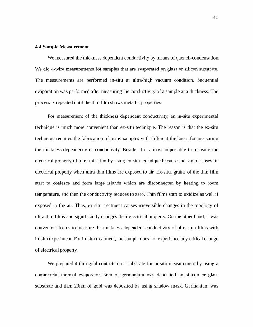
4.4 Sample Measurement……………………………………………...40
CHAPTER V EXPERIMENTAL RESULTS AND DISCUSSION…………….……….43
5.1 Experimental Results………………………………………………...43
5.1.1 Evaporation of Aluminum at Liquid Nitrogen……...…………43
5.2 Discussion…………………………………………………………...50
5.2.1 Linear Dependence of lnR and lnσ on 1/T………..…………50
5.2.2 Initial Value of the Resistance…………………...…………51
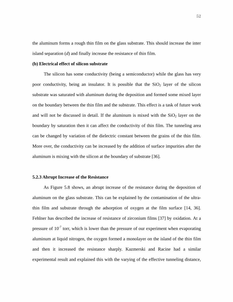
5.2.3 Abrupt Increase of the Resistance………………...…………52
CHAPTER VI CONCLUSION…………….…………………………………………….55
REFERENCES…………………………………………………………..……….………56
VITA…………………………………………………………………………...………58
viii
LIST OF FIGURES
Page
Figure 2.1 Schematic design of typical thermal evaporator………………………………3
Figure 2.2 Schematic design of quench condensation system……………………………5
Figure 2.3 Electron micrographs of thin Au films…………………………………………6
Figure 2.4 Potential energy versus distance from the surface of substrate and
interactions between atoms…………………………………………………7
Figure 2.5 Schematic of coalescence process………………………………………………9
Figure 2.6 AFM images of PbSe dots which shows ripening process……………………10
Figure 2.7 Conduction mechanism of thin film……………………………………………13
Figure 2.8 Experimental result of Kazmaerski and Racine………………………………14
Figure 2.9 Metal-insulator transition as quantum phase transition………………………16
Figure 3.1 Exterior view of an insertable cryostat and our quench-condensation
apparatus……………………………………………………………………18
Figure 3.2 Schematics of our quench-condensation apparatus……………………………19
Figure 3.3 The exterior view and schematic dimensions of 4He dewar…………………20
Figure 3.4 Indium O-ring flange…………………………………………………………22
Figure 3.5 Upper plate components………………………………………………………23
Figure 3.6 Lower plate components………………………………………………………24
Figure 3.7 Components on top of SQCA…………………………………………………25
Figure 4.1 Schematic of experimental procedure…………………………………………27
Figure 4.2 Commercial and hand made……………………………………………………30
ix
Page
Figure 4.3 Evaporation source after evaporation…………………………………………32
Figure 4.4 Quartz crystal microbalance (QCM) …………………………………………35
Figure 4.5 Radiation shield for QCM…………………………………………………36
Figure 4.6 Resonance frequency versus temperature of QCM at liquid nitrogen……37
Figure 4.7 Resonance frequency versus time of QCM at liquid nitrogen……………37
Figure 4.8 Sample preparation and measurement process………………………………42
Figure 5.1 Resistance versus temperature for 1st evaporation…………………………43
Figure 5.2 The increasing rate of conductivity to depend on inverse temperature……44
Figure 5.3 Resistance versus inverse temperature for d1 and d6………………………45
Figure 5.4 Logarithmic resistance versus inverse temperature for d1 and d6…………45
Figure 5.5 Resistance and lnR versus inverse temperature for d2~ d3……………………46
Figure 5.6 Resistance and lnR versus inverse temperature for d4~ d6……………………47
Figure 5.7 Resistance versus time for d1 and d2, is deposited on a glass……………48
Figure 5.8 Resistance versus temperature for d1 and d2………………………………49
Figure 5.9 lnR versus temperature for d1 and d2………………………………………49
Figure 5.10 Increase of the tunneling barrier by oxidation of thin film……………………53
x
LIST OF TABLES
Page
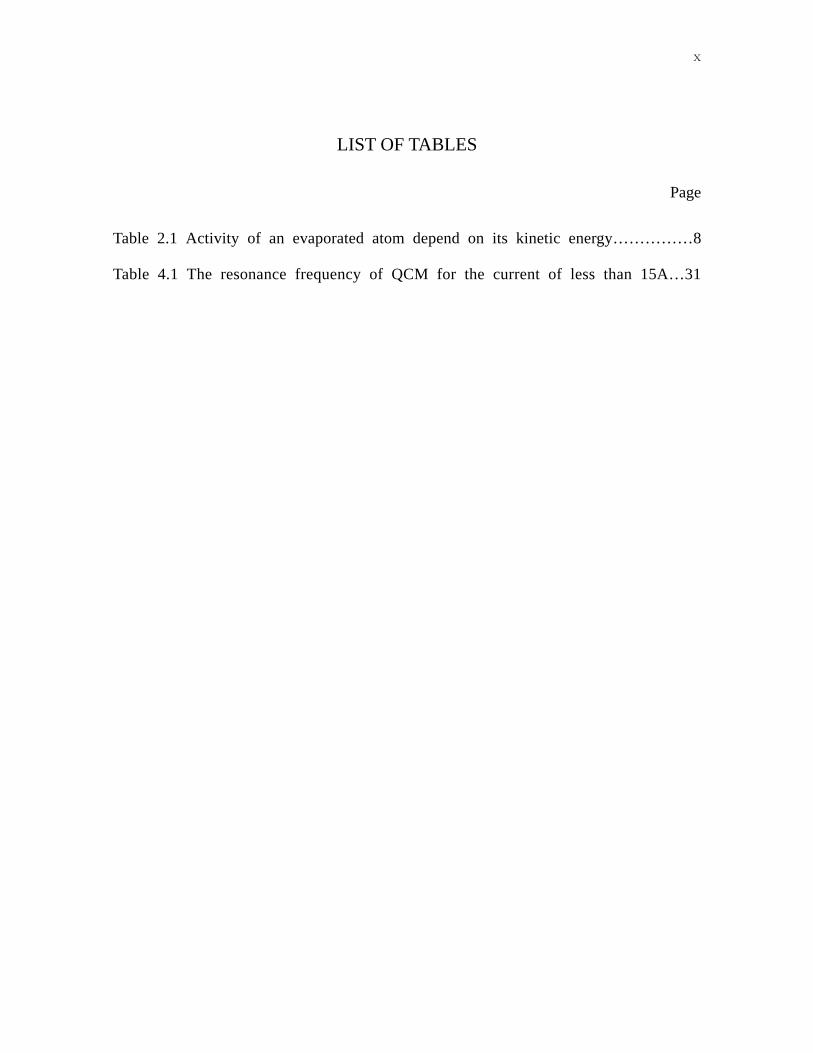
Table 2.1 Activity of an evaporated atom depend on its kinetic energy……………8
Table 4.1 The resonance frequency of QCM for the current of less than 15A…31
1
CHAPTER I
INTRODUCTION
1.1 Motivation
Materials have some interesting characteristics when they are in 2D thin film form, for
example, they can show a thickness or magnetic field driven metal-insulator transitions [1,
2] or superconductivity in the 2D regime [3, 4]. It is essential to use some special
techniques for such an experiment. For that reason, we designed and constructed an
experimental apparatus that can make high quality samples, using quench condensation.
1.2 Research Objective
The objective of this project is to measure the electrical conductivity of 2 dimensional
(2D) aluminum and nickel thin films deposited at low temperature using a home-built
quench-condensation apparatus. 2D thin films have been of great interest for several
decades and many theoretical models have been proposed [5~11]. In most experiments
metallic films are evaporated at room temperature and then cooled on a substrate [12~14].
We made an apparatus that can be immersed into liquid helium and then perform
evaporations at low temperature. We have performed an in-situ experiment with this newly
designed apparatus on the 2D conductivity of thin films.
This thesis follows the style of Physical Review Letters.
2
CHAPTER II
BACKGROUND
Materials have many interesting properties when they are in form of a very thin film.
They have distinguishable physical characteristics and significantly different electrical
properties depending on the growth process [14~16]. Many physical models have been
proposed to describe the relation between physical characteristics and electrical properties
[5~11]. Typically, they can be categorized into classical and quantum mechanical models.
For thin films with large grains the electrical conduction can be explained by thermal
activation and tunneling effects [14]. On the other hand, for ultra thin films with small
granular grains, experimental results show anomalous behavior that is not expected from
classical models [3]. In this chapter, we will focus on understanding the electrical properties
and the growth process of thin films. Furthermore, we will introduce the basic techniques of
thin film fabrication for understanding the importance of our experimental technique, which
is applied to get the expected experiment results on the electrical properties of thin films.
2.1 Thermal Evaporation
Thermal evaporation is the simplest deposition technique to deposit various materials
by a physical deposition process. Materials are heated to evaporate by applying a high
electric current and then deposited onto a substrate to form a thin film. The evaporation
occurs in a high vacuum where the mean free path of the incident atoms is much longer
than the distance from the evaporation source to the substrate. Therefore, evaporated atoms
are incident by ballistic motion and then deposit onto the exposed surface of a substrate
3
forming a thin film.
Rough
pump
Substrate
holder Thickness
monitor
Evaporation
source
Bell jar
Pressure
sensor
High vacuum
pump
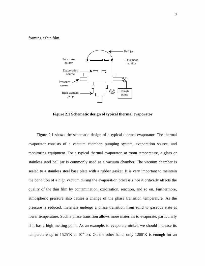
Figure 2.1 Schematic design of typical thermal evaporator
Figure 2.1 shows the schematic design of a typical thermal evaporator. The thermal
evaporator consists of a vacuum chamber, pumping system, evaporation source, and
monitoring equipment. For a typical thermal evaporator, at room temperature, a glass or
stainless steel bell jar is commonly used as a vacuum chamber. The vacuum chamber is
sealed to a stainless steel base plate with a rubber gasket. It is very important to maintain
the condition of a high vacuum during the evaporation process since it critically affects the
quality of the thin film by contamination, oxidization, reaction, and so on. Furthermore,
atmospheric pressure also causes a change of the phase transition temperature. As the
pressure is reduced, materials undergo a phase transition from solid to gaseous state at
lower temperature. Such a phase transition allows more materials to evaporate, particularly
if it has a high melting point. As an example, to evaporate nickel, we should increase its
temperature up to 1525˚K at 10-4torr. On the other hand, only 1200˚K is enough for an
4
evaporation at 10-8torr. Both rough pumps and high vacuum pumps form the basic pumping
system to produce a high vacuum inside the chamber. A rough pump is capable of reaching
a pressure of at most P=10-4torr, while a high vacuum pump reaches P=10-6~10-8 torr.
Generally, a diffusion pump, a turbo molecular pump or a cryopump is used for high
vacuum pumping. Materials to be evaporated (evaporant) are held by evaporation sources,
like a crucible, boat or wire coil. Tungsten wire is commonly used as an evaporation source
for materials like aluminum, nickel, chromium, gold, lead, and so on. A quartz crystal
microbalance (QCM) is used to measure the thickness of the sample and an ion gauge
monitors the vacuum. Additional monitoring equipment can be added depending on
experimental purposes.
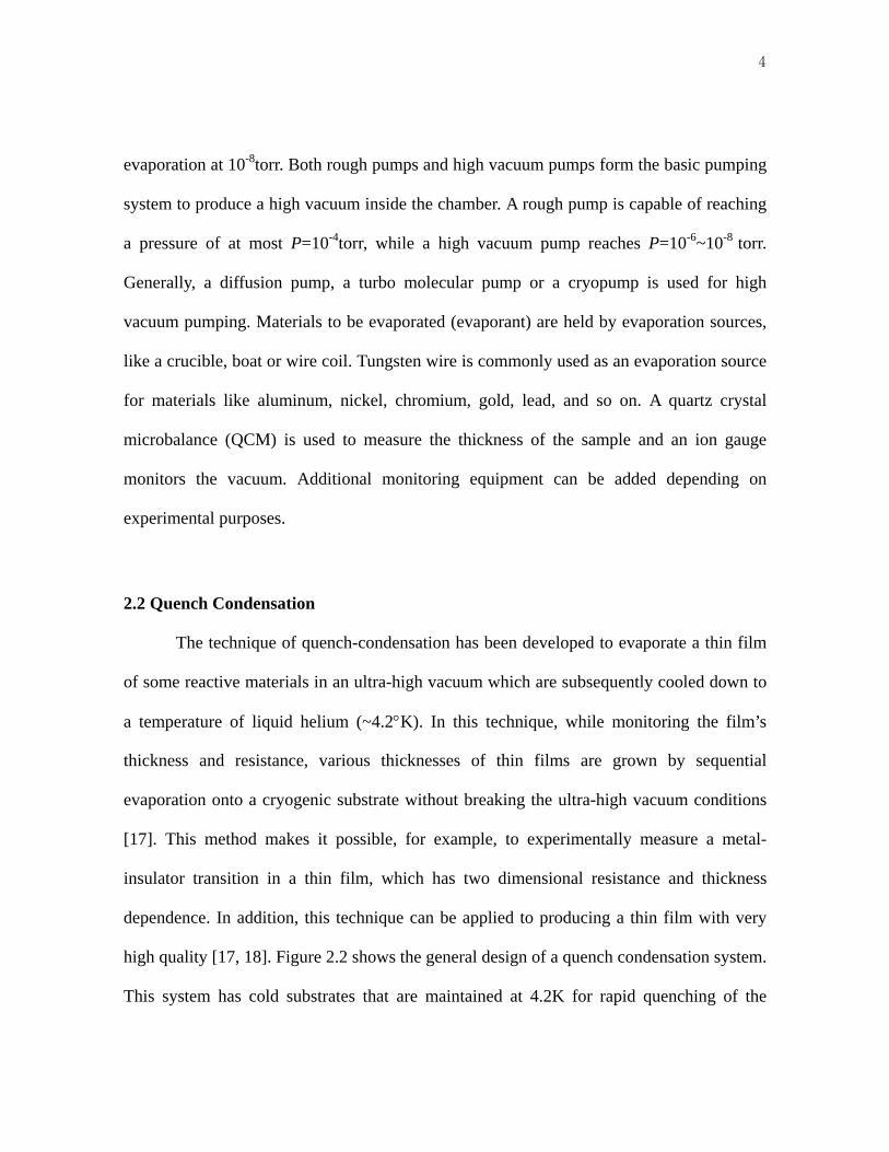
2.2 Quench Condensation
The technique of quench-condensation has been developed to evaporate a thin film
of some reactive materials in an ultra-high vacuum which are subsequently cooled down to
a temperature of liquid helium (~4.2°K). In this technique, while monitoring the film’s
thickness and resistance, various thicknesses of thin films are grown by sequential
evaporation onto a cryogenic substrate without breaking the ultra-high vacuum conditions
[17]. This method makes it possible, for example, to experimentally measure a metal-
insulator transition in a thin film, which has two dimensional resistance and thickness
dependence. In addition, this technique can be applied to producing a thin film with very
high quality [17, 18]. Figure 2.2 shows the general design of a quench condensation system.
This system has cold substrates that are maintained at 4.2K for rapid quenching of the
5
evaporant. Generally the evaporation source is installed at T > 4.2K, while the path between
the substrate and the source is blocked by a shutter.
He4
(4.2°K)
Above 4.2°K
Cold substrate
Shutter
Evaporation source
Figure 2.2 Schematic design of quench condensation system
2.3 Growth Process of a Thin Film
2.3.1 Introduction
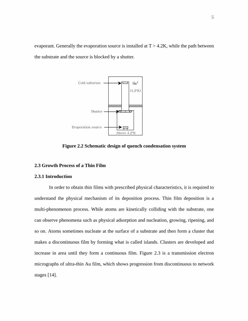
In order to obtain thin films with prescribed physical characteristics, it is required to
understand the physical mechanism of its deposition process. Thin film deposition is a
multi-phenomenon process. While atoms are kinetically colliding with the substrate, one
can observe phenomena such as physical adsorption and nucleation, growing, ripening, and
so on. Atoms sometimes nucleate at the surface of a substrate and then form a cluster that
makes a discontinuous film by forming what is called islands. Clusters are developed and
increase in area until they form a continuous film. Figure 2.3 is a transmission electron
micrographs of ultra-thin Au film, which shows progression from discontinuous to network
stages [14].
6
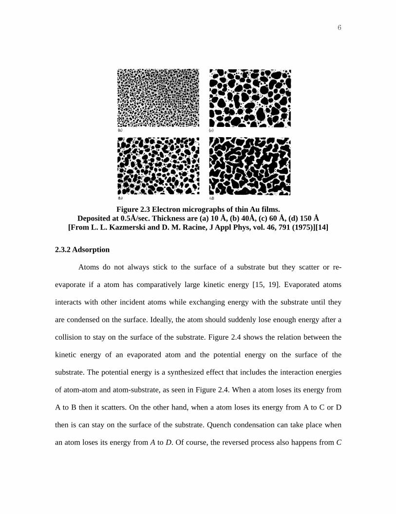
Figure 2.3 Electron micrographs of thin Au films. Deposited at 0.5Å/sec. Thickness are (a) 10 Å, (b) 40Å, (c) 60 Å, (d) 150 Å
[From L. L. Kazmerski and D. M. Racine, J Appl Phys, vol. 46, 791 (1975)][14]
2.3.2 Adsorption
Atoms do not always stick to the surface of a substrate but they scatter or re-
evaporate if a atom has comparatively large kinetic energy [15, 19]. Evaporated atoms
interacts with other incident atoms while exchanging energy with the substrate until they
are condensed on the surface. Ideally, the atom should suddenly lose enough energy after a
collision to stay on the surface of the substrate. Figure 2.4 shows the relation between the
kinetic energy of an evaporated atom and the potential energy on the surface of the
substrate. The potential energy is a synthesized effect that includes the interaction energies
of atom-atom and atom-substrate, as seen in Figure 2.4. When a atom loses its energy from
A to B then it scatters. On the other hand, when a atom loses its energy from A to C or D
then is can stay on the surface of the substrate. Quench condensation can take place when
an atom loses its energy from A to D. Of course, the reversed process also happens from C
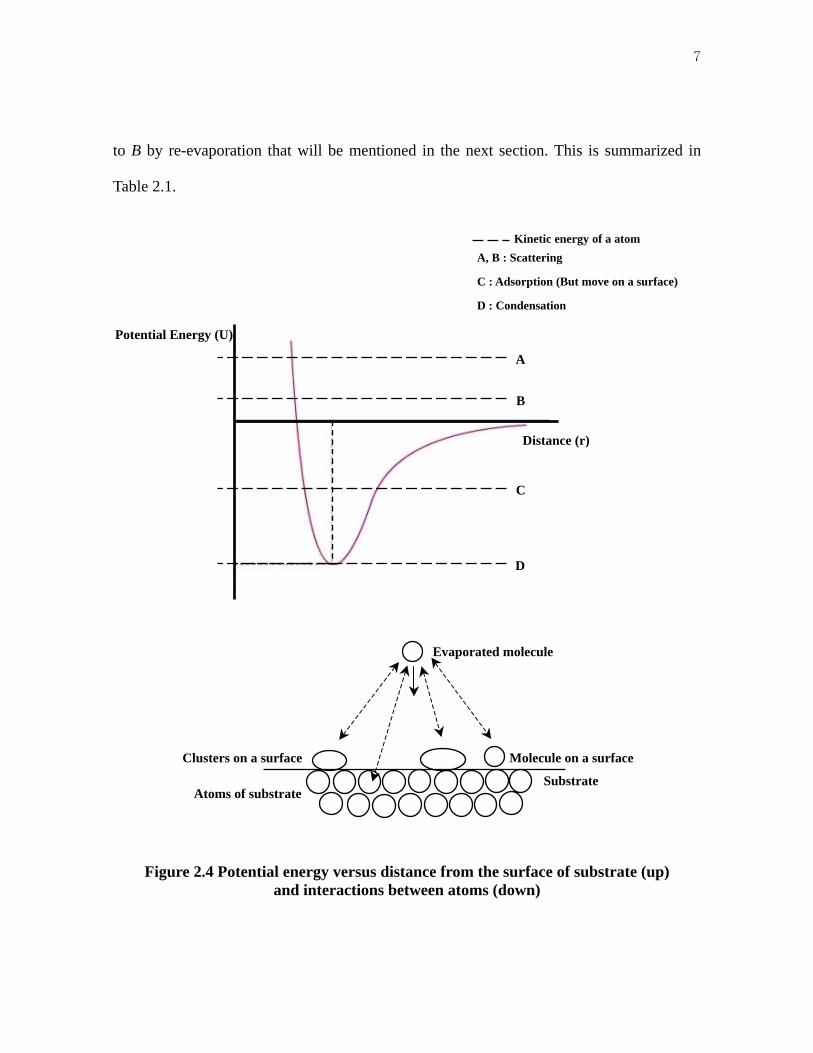
7
to B by re-evaporation that will be mentioned in the next section. This is summarized in
Table 2.1.
A, B : Scattering
C : Adsorption (But move on a surface)
D : Condensation
Kinetic energy of a atom
A
B
C
D
Potential Energy (U)
Distance (r)
Substrate
Evaporated molecule
Atoms of substrate
Clusters on a surface Molecule on a surface
Figure 2.4 Potential energy versus distance from the surface of substrate (up) and interactions between atoms (down)
8
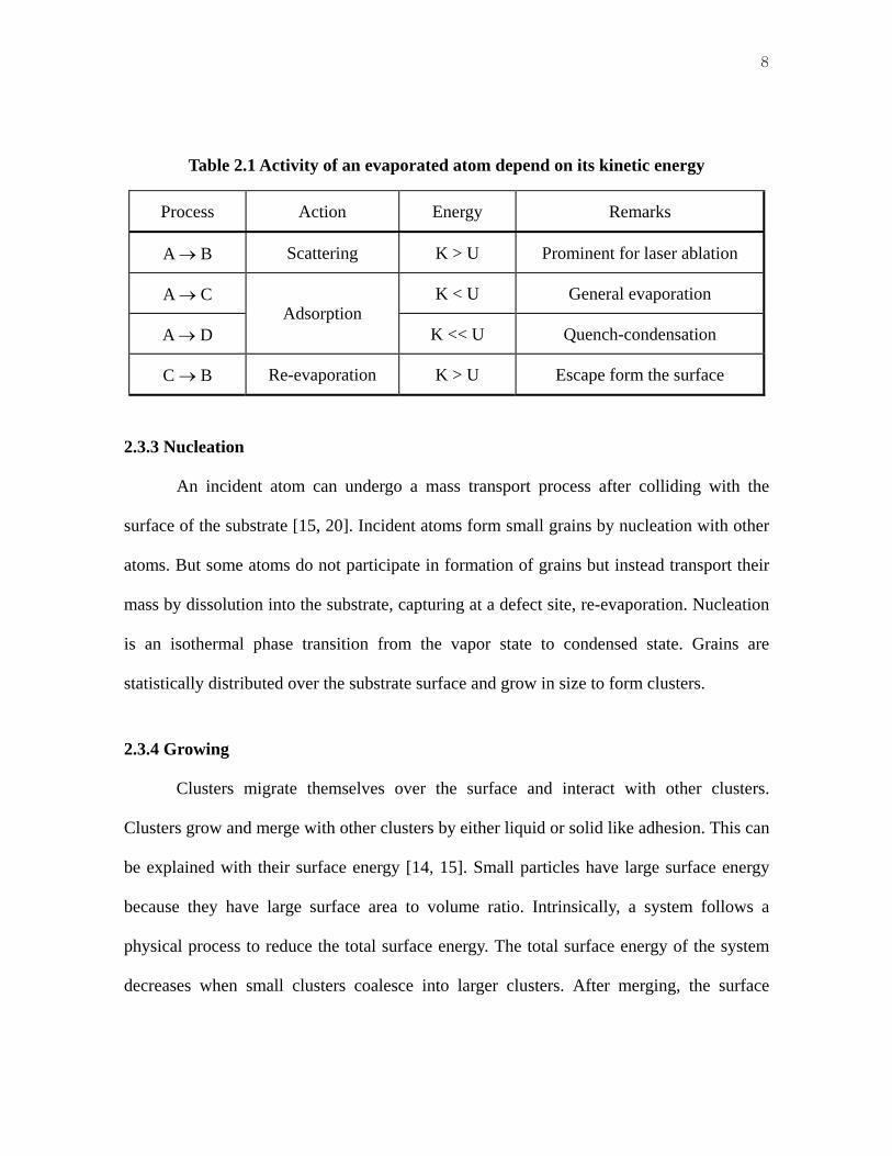
Table 2.1 Activity of an evaporated atom depend on its kinetic energy
Process Action Energy Remarks
A → B Scattering K > U Prominent for laser ablation
A → C K < U General evaporation
A → D Adsorption
K << U Quench-condensation
C → B Re-evaporation K > U Escape form the surface
2.3.3 Nucleation
An incident atom can undergo a mass transport process after colliding with the
surface of the substrate [15, 20]. Incident atoms form small grains by nucleation with other
atoms. But some atoms do not participate in formation of grains but instead transport their
mass by dissolution into the substrate, capturing at a defect site, re-evaporation. Nucleation
is an isothermal phase transition from the vapor state to condensed state. Grains are
statistically distributed over the substrate surface and grow in size to form clusters.
2.3.4 Growing
Clusters migrate themselves over the surface and interact with other clusters.
Clusters grow and merge with other clusters by either liquid or solid like adhesion. This can
be explained with their surface energy [14, 15]. Small particles have large surface energy
because they have large surface area to volume ratio. Intrinsically, a system follows a
physical process to reduce the total surface energy. The total surface energy of the system
decreases when small clusters coalesce into larger clusters. After merging, the surface
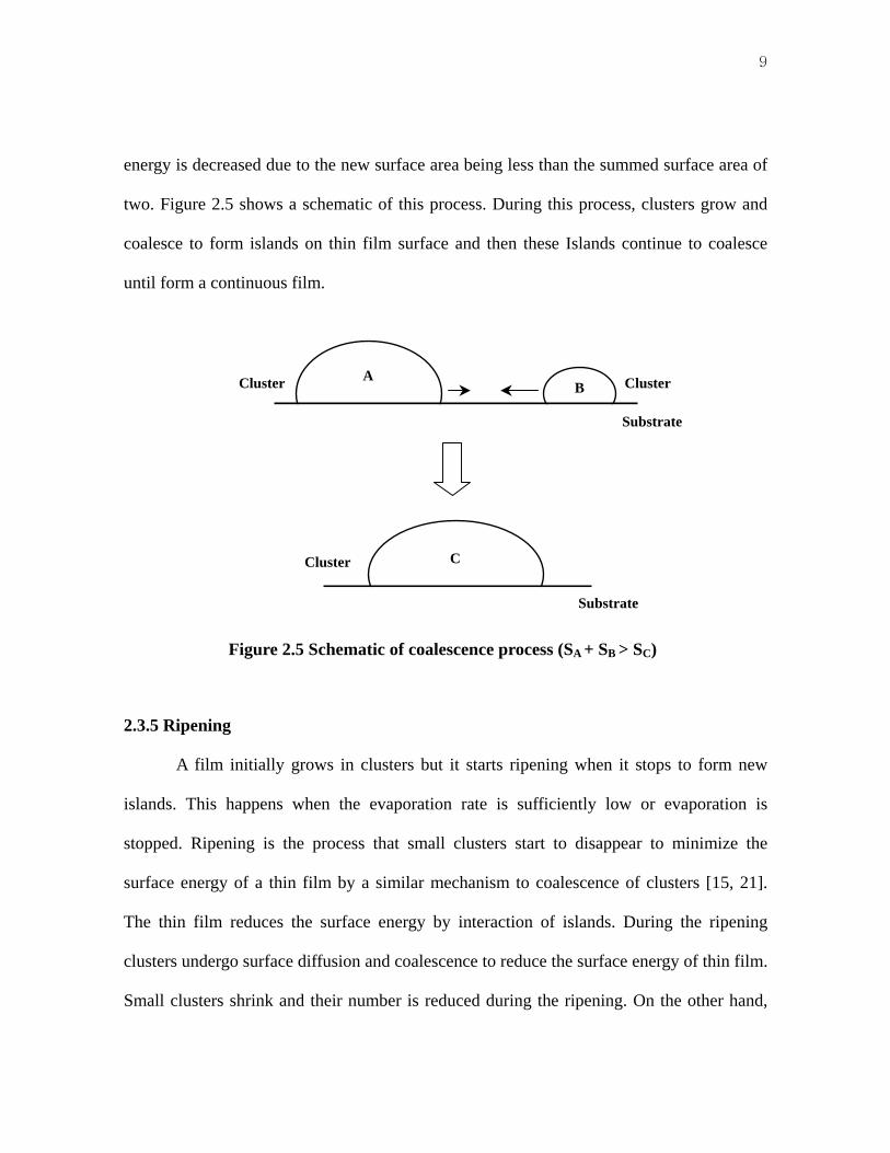
9
energy is decreased due to the new surface area being less than the summed surface area of
two. Figure 2.5 shows a schematic of this process. During this process, clusters grow and
coalesce to form islands on thin film surface and then these Islands continue to coalesce
until form a continuous film.
A B
C
Substrate
Substrate
Cluster
Cluster Cluster
Figure 2.5 Schematic of coalescence process (SA + SB > SC)
2.3.5 Ripening
A film initially grows in clusters but it starts ripening when it stops to form new
islands. This happens when the evaporation rate is sufficiently low or evaporation is
stopped. Ripening is the process that small clusters start to disappear to minimize the
surface energy of a thin film by a similar mechanism to coalescence of clusters [15, 21].
The thin film reduces the surface energy by interaction of islands. During the ripening
clusters undergo surface diffusion and coalescence to reduce the surface energy of thin film.
Small clusters shrink and their number is reduced during the ripening. On the other hand,
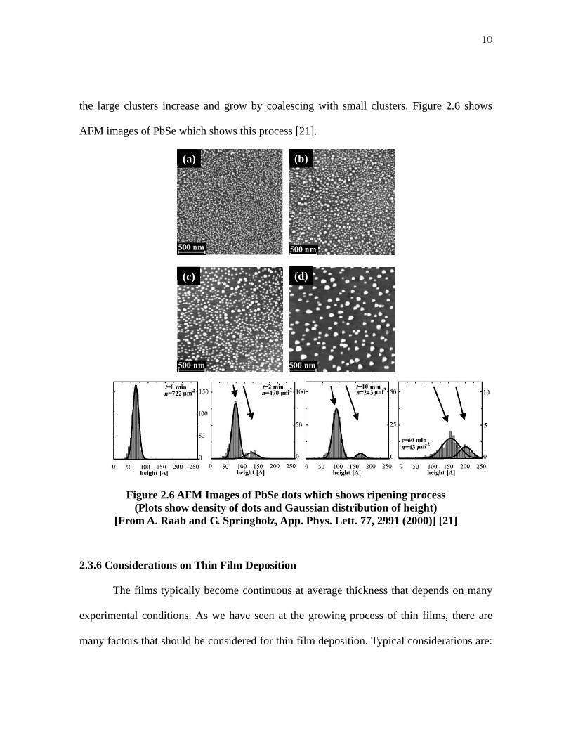
10
the large clusters increase and grow by coalescing with small clusters. Figure 2.6 shows
AFM images of PbSe which shows this process [21].
(b)(a)
(d)(c)
Figure 2.6 AFM Images of PbSe dots which shows ripening process (Plots show density of dots and Gaussian distribution of height)
[From A. Raab and G. Springholz, App. Phys. Lett. 77, 2991 (2000)] [21]
2.3.6 Considerations on Thin Film Deposition
The films typically become continuous at average thickness that depends on many
experimental conditions. As we have seen at the growing process of thin films, there are
many factors that should be considered for thin film deposition. Typical considerations are:
11
the evaporation rate and the temperature of substrate, the type of material to be evaporated
(evaporant) and substrate, and so on. The island size significantly depends on the
evaporation rate and the temperature of substrate. Thin films have larger island size for
higher evaporation rates or substrate temperatures since the surface mobility of clusters is
enhanced with increasing surface energy [16]. The specific of evaporant also affects the
deposition of a thin film. As a good example, gold has poor adhesion compared to other
materials so it is difficult to form a thin film on silicon or a glass substrate. Therefore, we
should pre-evaporate germanium, chromium or titanium to form a gold thin film on the
substrate. Besides, the nature of substrate also affects the thin film deposition since it has
varying topology and the adhesion depends on its character. Porousness and adhesion of the
substrate affects the saturation and nucleation of atoms that affects the island size of thin
film. Roughness and defects of the surface affects the uniformity of a thin film. Chemical
stability and impurities of the substrate also affects the properties of a thin film [16].
2.4 Electrical Properties of Thin Films
2.4.1 Introduction
A material has many interesting properties when it is in form of a thin film. A metal
can have nonmetallic properties in form of a very thin film [22]. On the other hand, an
insulator can have metallic properties when it is in form of a thin film in some unique
circumstances [23]. Besides, thin films of magnetic materials can show a metal-insulator
transition when tuned by a magnetic field [1, 2]. A superconducting thin films like Pb, Al,
Sn has nonmetallic property when it is very thin and then it transforms to a superconductor
12
when grown to be thicker [22]. VO2 shows a transition of its electronic properties from
insulating to metallic [23]. GdxSi1-x and Ni shows a magnetic field driven metal-insulator
transition by application of a magnetic field [1~2]. Indeed, the electrical properties of a thin
film are unique and sometimes quite different from materials in bulk condition. As we have
seen at the thin film growth process, discontinuous growth of a thin film is a very important
feature and we will use this as a starting point to explain the electric transport properties of
a thin film.
2.4.2 Basic Models
In general, physical models for the electronic properties of a thin film can be
categorized into two different ways by their physical condition. One is for a thin film
forming islands, whose electronic properties are commonly explained by thermal activation
and tunneling effects between the islands [5]. Another is for superconducting thin films, for
which more quantum mechanical models are required to explain the electronic properties [3,
4].
Neugebauer and Webb proposed a simple model that explains conductivity of thin
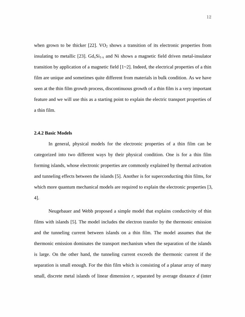
films with islands [5]. The model includes the electron transfer by the thermonic emission
and the tunneling current between islands on a thin film. The model assumes that the
thermonic emission dominates the transport mechanism when the separation of the islands
is large. On the other hand, the tunneling current exceeds the thermonic current if the
separation is small enough. For the thin film which is consisting of a planar array of many
small, discrete metal islands of linear dimension r, separated by average distance d (inter
13
island separation) the number of charged islands is described as
kTNenε−
= (1)
where N is the total number of islands in the film and ε is the effective activation energy
which is ε≈q2/r. q is the charge of a carrier (electron). The tunneling probability of an
electron from one negatively charged island (i) to the neighboring islands (f) is
(2) ∫∞
∞−−∝ εdfDfP ji )1(
where f is the Fermi function and D is the transmission coefficient. Figure 2.7 shows a
conduction mechanism of thin film.
d
r
i f
Substrate
Island h
(a) Islands on a substrate
f i h
ε =0
Potential barrier
(b) Schematic of the conduction mechanism by Neugebauer and Webb [5]
Figure 2.7 Conduction mechanism of thin film
14
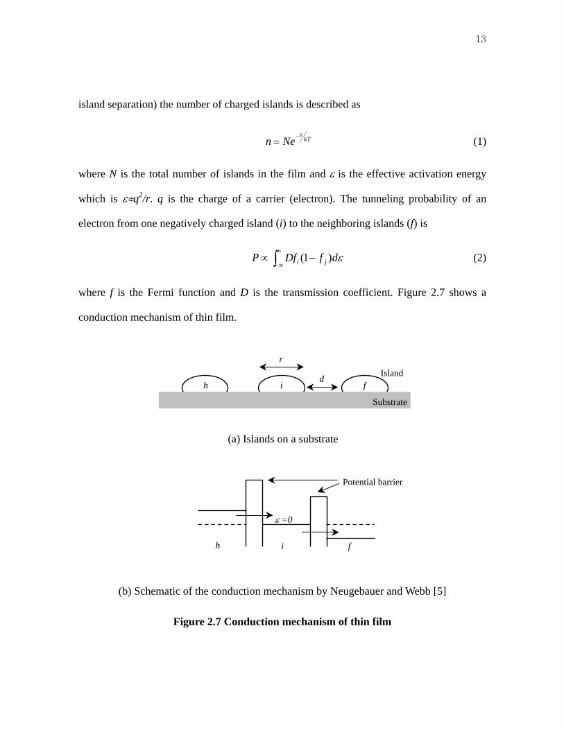
The conductivity is described as
⎟⎟⎟
⎠
⎞
⎜⎜⎜
⎝
⎛−∝
kTr
qDqd
r
2
22 exp1σ (3)
where D is the transmission coefficient, r is the effective island size and d is the distance
between islands (inter island separation).
Figure 2.8 shows the experimental result of Kazmerski and Racine which
investigated the conduction mechanism of ultra-thin (10~100Å) metalic films [14].
Figure 2.8 Experimental result of Kazmerski and Racine [14]
[From L. L. Kazmerski and D. M. Racine, J Appl Phys, vol. 46, 791 (1975)][14]
15
The experimental result shows agreement with the model of Neugebauer and Webb which
predicts a linear dependence of the logarithmic scale of conductivity (lnσ).
Another model, which was experimentally proven by A. Frydman and R.C. Dynes,
explains the superconducting transition based on its critical behavior [3, 4]. For quench-
condensed granular thin films, the sheet resistance versus temperature for T<Tc follows and
exponential behavior and can be expressed in the following way.
00
TTeRR = (4)
where Ro is the value of the resistance obtained by extrapolating the R-T curves to T=0 and
T0 is its temperature. Though the cause for this dependence is not fully understood, it turns
out to be universal for two-dimensional (2D) granular superconducting thin films. In this
model, the equation does not depend on the nature of the superconducting grains but only
on the geometrical arrangement of the grains which is affected by the specifics of the thin
film deposition.
2.4.3 Metal-Insulator Transition in a Thin Film
The electrical conductivity of a material can be changed from metal to insulator or
vice versa by its physical condition. This transition is well known as metal-insulator
transition and has been studied for a long time [24~31]. Scientists tried to understand its
physical principles by studying some transitions from metal to insulator after Wilson gave a
description of the difference between metals and insulators in 1931 [24]. The area of
research has been broadened by development of experimental techniques and subsequently
16
topics such as a magnetic field driven metal-insulator transition [1, 2], hole driven metal-
insulator transition [23] were studied.
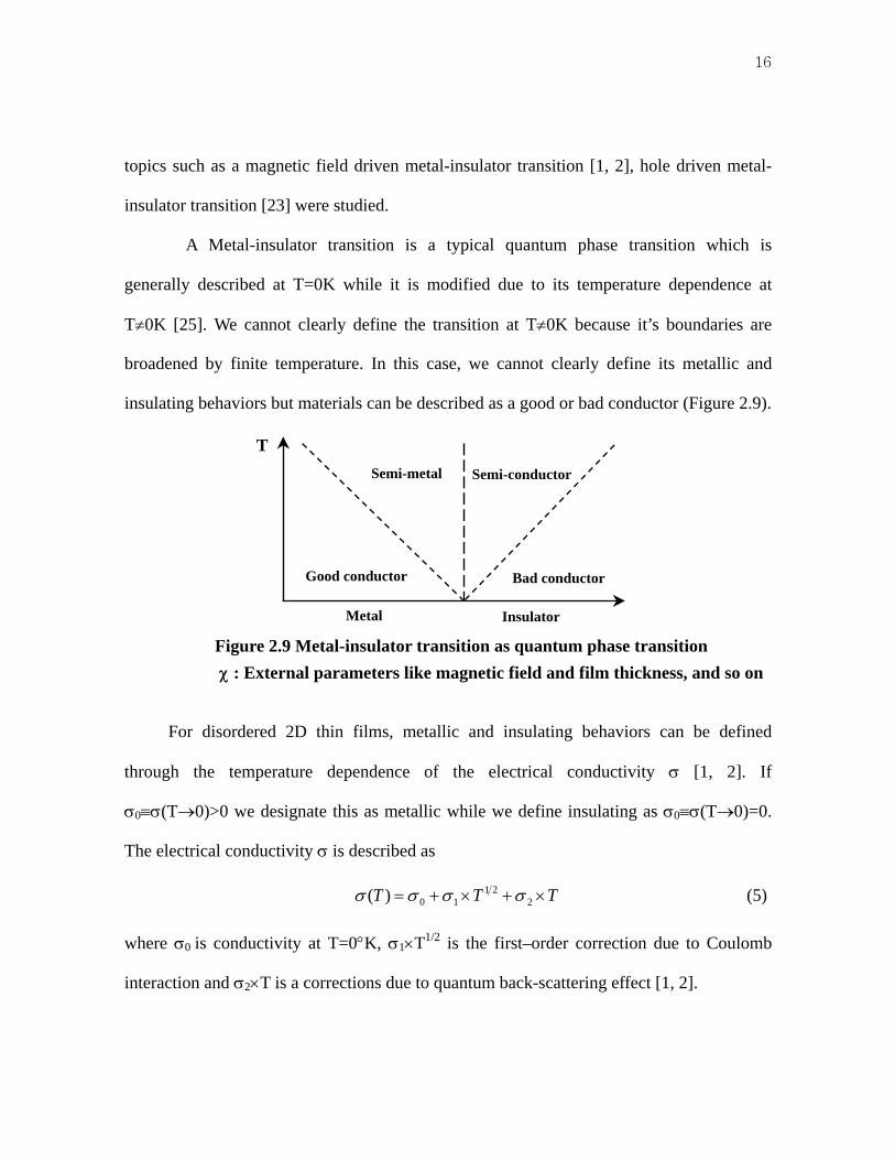
A Metal-insulator transition is a typical quantum phase transition which is
generally described at T=0K while it is modified due to its temperature dependence at
T≠0K [25]. We cannot clearly define the transition at T≠0K because it’s boundaries are
broadened by finite temperature. In this case, we cannot clearly define its metallic and
insulating behaviors but materials can be described as a good or bad conductor (Figure 2.9).
T
Semi-conductorSemi-metal
Good conductor Bad conductor
Insulator Metal
Figure 2.9 Metal-insulator transition as quantum phase transition χ : External parameters like magnetic field and film thickness, and so on
For disordered 2D thin films, metallic and insulating behaviors can be defined
through the temperature dependence of the electrical conductivity σ [1, 2]. If
σ0≡σ(T→0)>0 we designate this as metallic while we define insulating as σ0≡σ(T→0)=0.
The electrical conductivity σ is described as
TTT ×+×+= 221
10)( σσσσ (5)
where σ0 is conductivity at T=0°K, σ1×T1/2 is the first–order correction due to Coulomb
interaction and σ2×T is a corrections due to quantum back-scattering effect [1, 2].
17
CHAPTER III
QUENCH-CONDENSATION APPARATUS
As we discussed in the previous chapter, two-dimensional (2D) thin films were known
to show very unique electrical properties that were successfully described based on
quantum mechanical models. Until now, several methods have been used to deposit thin
films at room temperature but these techniques were not enough to investigate the 2D
electrical properties. In this case, samples were dominated by bulk properties including the
thermal activation. On the other hand, the quench-condensation technique enabled the
investigation of 2D thin film. We designed and built a very simple apparatus that can be
immersed into liquid helium and then perform quench-condensation with in-situ
measurement at low temperature.
3.1 Design Overview
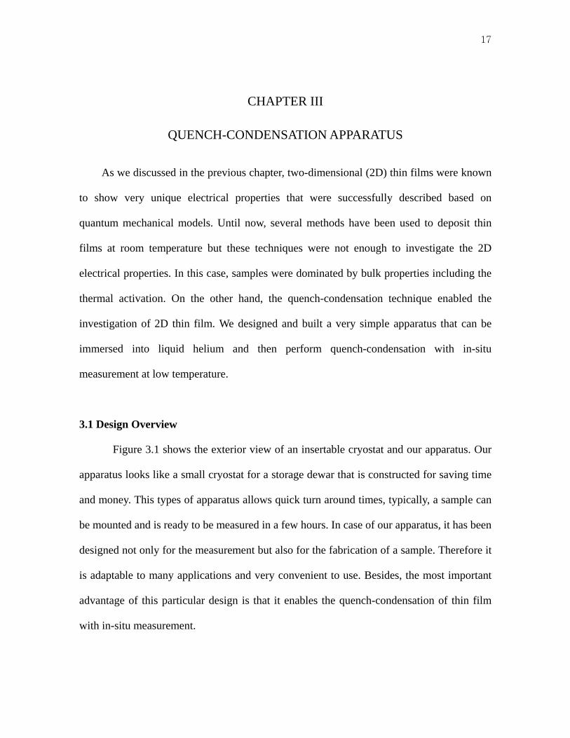
Figure 3.1 shows the exterior view of an insertable cryostat and our apparatus. Our
apparatus looks like a small cryostat for a storage dewar that is constructed for saving time
and money. This types of apparatus allows quick turn around times, typically, a sample can
be mounted and is ready to be measured in a few hours. In case of our apparatus, it has been
designed not only for the measurement but also for the fabrication of a sample. Therefore it
is adaptable to many applications and very convenient to use. Besides, the most important
advantage of this particular design is that it enables the quench-condensation of thin film
with in-situ measurement.
18
Figure 3.1 Exterior view of an insertable cryostat (left) and our quench-condensation apparatus (right)
19
Pumping Valve
Shutter actuation handle (Motion feedthrough)
Wire connector (Electronic Feedthrough)
Tube line brace
Flange holder (Adjustable by screw) He4 dewar cover Flange
Pumping & wire line
Shutter actuation line
Upper plate
Lower plate
Thermometer
QCM
Radiation shield
Substrate mounting plate
Substrate
Shutter
Radiation jacket
Vacuum chamber
Evaporation Source
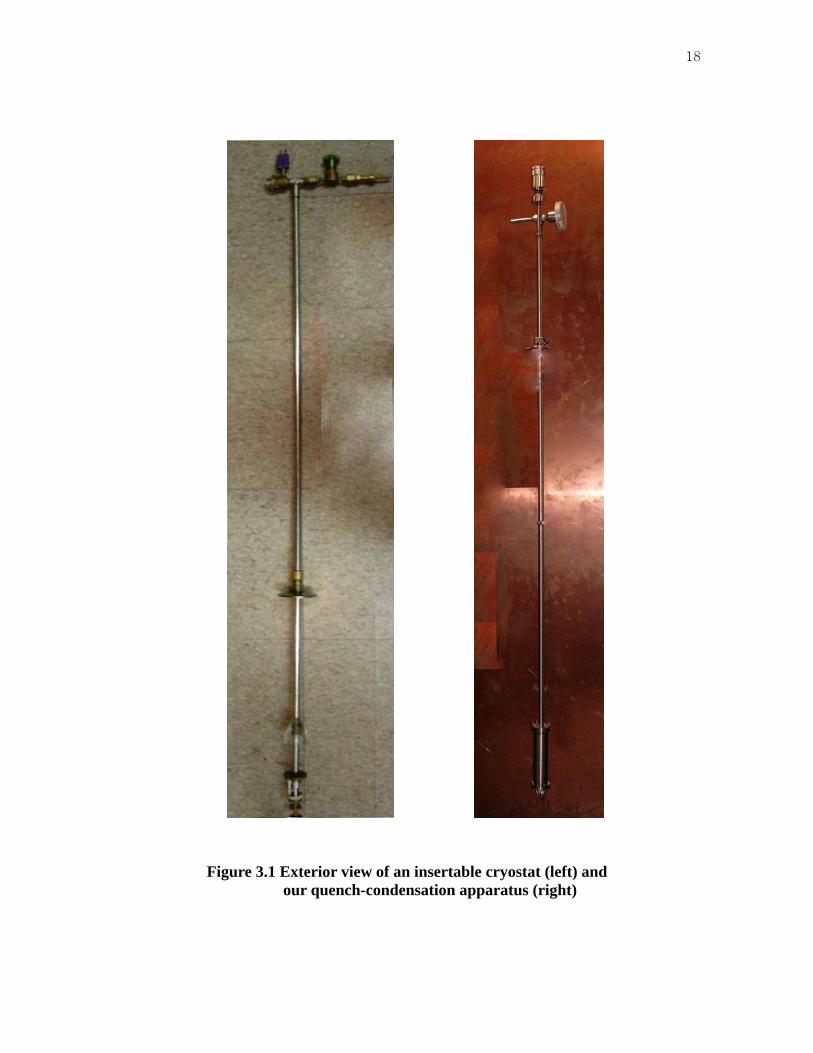
Figure 3.2 Schematics of our quench-condensation apparatus
20
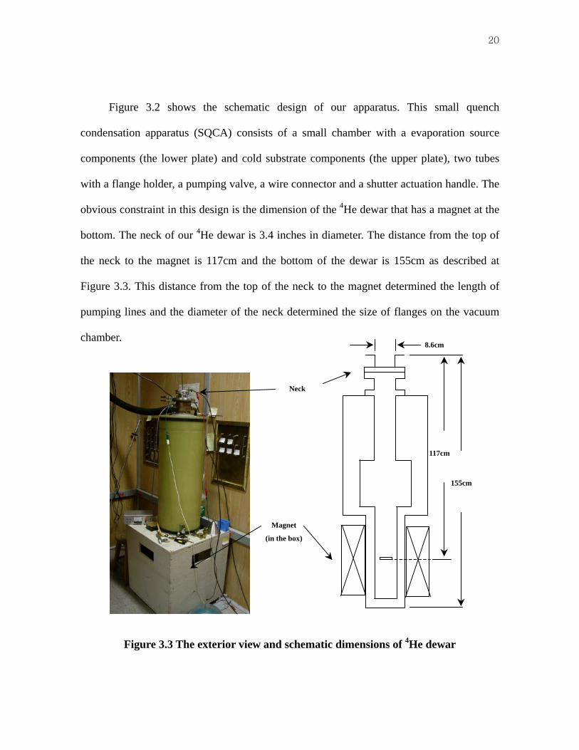
Figure 3.2 shows the schematic design of our apparatus. This small quench
condensation apparatus (SQCA) consists of a small chamber with a evaporation source
components (the lower plate) and cold substrate components (the upper plate), two tubes
with a flange holder, a pumping valve, a wire connector and a shutter actuation handle. The
obvious constraint in this design is the dimension of the 4He dewar that has a magnet at the
bottom. The neck of our 4He dewar is 3.4 inches in diameter. The distance from the top of
the neck to the magnet is 117cm and the bottom of the dewar is 155cm as described at
Figure 3.3. This distance from the top of the neck to the magnet determined the length of
pumping lines and the diameter of the neck determined the size of flanges on the vacuum
chamber.
Magnet
(in the box)
Neck
8.6cm
155cm
117cm
Figure 3.3 The exterior view and schematic dimensions of 4He dewar
21
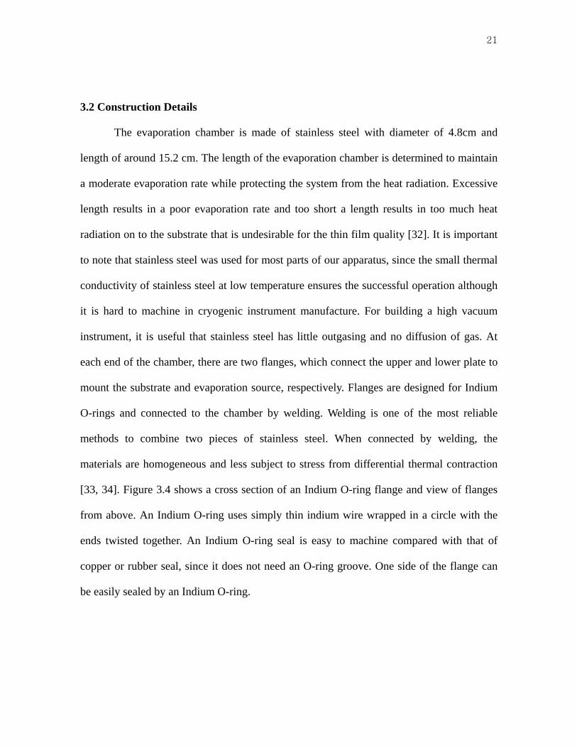
3.2 Construction Details
The evaporation chamber is made of stainless steel with diameter of 4.8cm and
length of around 15.2 cm. The length of the evaporation chamber is determined to maintain
a moderate evaporation rate while protecting the system from the heat radiation. Excessive
length results in a poor evaporation rate and too short a length results in too much heat
radiation on to the substrate that is undesirable for the thin film quality [32]. It is important
to note that stainless steel was used for most parts of our apparatus, since the small thermal
conductivity of stainless steel at low temperature ensures the successful operation although
it is hard to machine in cryogenic instrument manufacture. For building a high vacuum
instrument, it is useful that stainless steel has little outgasing and no diffusion of gas. At
each end of the chamber, there are two flanges, which connect the upper and lower plate to
mount the substrate and evaporation source, respectively. Flanges are designed for Indium
O-rings and connected to the chamber by welding. Welding is one of the most reliable
methods to combine two pieces of stainless steel. When connected by welding, the
materials are homogeneous and less subject to stress from differential thermal contraction
[33, 34]. Figure 3.4 shows a cross section of an Indium O-ring flange and view of flanges
from above. An Indium O-ring uses simply thin indium wire wrapped in a circle with the
ends twisted together. An Indium O-ring seal is easy to machine compared with that of
copper or rubber seal, since it does not need an O-ring groove. One side of the flange can
be easily sealed by an Indium O-ring.
22
Indium wire
Figure 3.4 Indium O-ring flange
An Indium O-ring seal is reliable for a cryogenic seal unlike a rubber O-ring seal since
rubber is no longer elastomeric[33] at low temperature. However one should be careful to
use the Indium sealed apparatus for evaporation at room temperature as Indium melts at
high temperature around 430K. This apparatus should be used only for certain materials
that have low melting point when it is applied to room temperature evaporation. For
example, aluminum can be evaporated at room temperature with the Indium O-ring sealed
apparatus, while nickel cannot. Certainly, this is not a problem when using quench-
condensation because the flange always remains at low temperature in that case. 8 holes for
assembly and 4 holes for wire paths are drilled into the flange. 2 more holes are drilled into
the flanges of the upper and lower plate in order to readily allow detachment after usage.
The upper plate with flange is connected to two tubes by welding as can be seen in
Figure 3.2. We used thin-walled stainless steel tube because of its low thermal conductivity
and high strength. One of the tubes is for the path of the shutter actuation rod and another is
for the pumping line. Wires for measurement also pass through the pumping line. Figure
3.5 shows components of the upper plate. A substrate was placed on a 3.31cm-diameter
circular shape substrate mounting plate that is directly connected to the upper plate with
23
small spacer rod. We used OFHC copper for these parts because it is an excellent conductor
and good for vacuum instrumentation. The substrate maintains a temperature of 4K because
of this direct thermal connection to the chamber wall. A Cernox CX-1050 thin film
resistance sensor is mounted on the backside of the substrate mounting plate. A Quartz
Crystal Microbalance sensor (QCM) of 5MHz is attached at a small OFHC copper plate
that is mounted on the substrate mounting plate. For protection, the QCM is radiation
shielded with 4 copper baffles and a stainless steel box. A shadow mask is attached to the
substrate by 0-80 screws and spacers. A shutter is made of stainless steel and attached to the
shutter actuation rod by welding. The rod is made of stainless steel tube that is sealed into
an other tube. 16 wires are connected to the substrate by two detachable 16-pin sockets.
Thermometer
QCM (with radiation shields)
Pumping & Wire tube Tube for shutter
actuation rod
Shutter actuation rod
Shutter
16-pin socket
Shadow mask Substrate
Spacer
Substrate mounting plate
Figure 3.5 Upper plate components
24
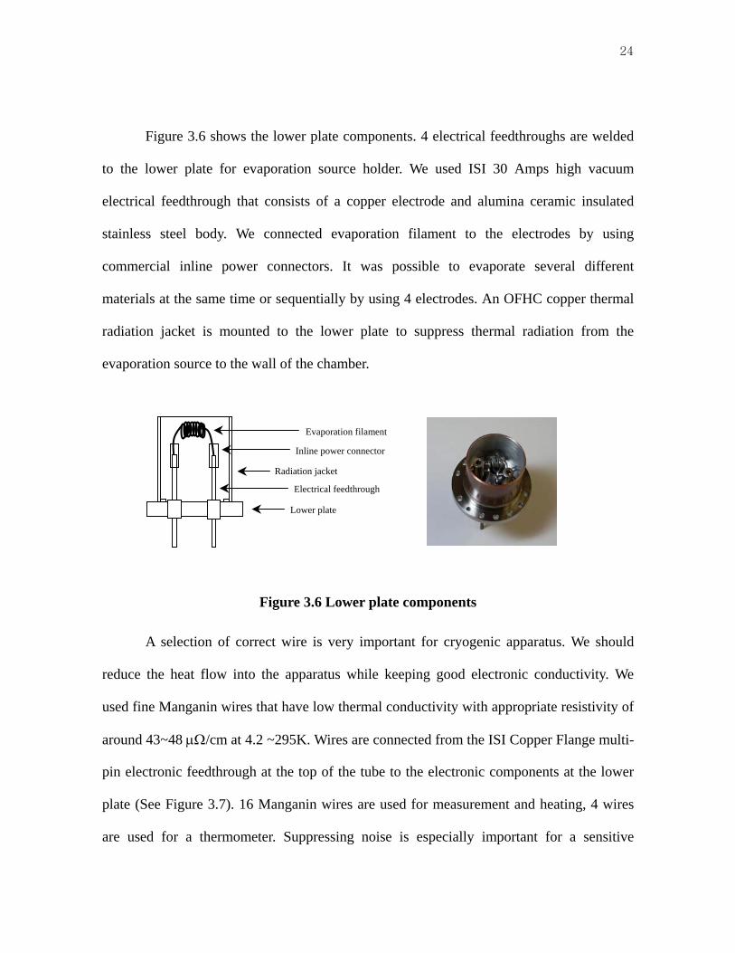
Figure 3.6 shows the lower plate components. 4 electrical feedthroughs are welded
to the lower plate for evaporation source holder. We used ISI 30 Amps high vacuum
electrical feedthrough that consists of a copper electrode and alumina ceramic insulated
stainless steel body. We connected evaporation filament to the electrodes by using
commercial inline power connectors. It was possible to evaporate several different
materials at the same time or sequentially by using 4 electrodes. An OFHC copper thermal
radiation jacket is mounted to the lower plate to suppress thermal radiation from the
evaporation source to the wall of the chamber.
Evaporation filament
Inline power connector
Radiation jacket
Electrical feedthrough
Lower plate
Figure 3.6 Lower plate components
A selection of correct wire is very important for cryogenic apparatus. We should
reduce the heat flow into the apparatus while keeping good electronic conductivity. We
used fine Manganin wires that have low thermal conductivity with appropriate resistivity of
around 43~48 μΩ/cm at 4.2 ~295K. Wires are connected from the ISI Copper Flange multi-
pin electronic feedthrough at the top of the tube to the electronic components at the lower
plate (See Figure 3.7). 16 Manganin wires are used for measurement and heating, 4 wires
are used for a thermometer. Suppressing noise is especially important for a sensitive
25
measurement with high frequency. We used coaxial wires for the QCM to suppress noise
during its sensitive measurement. Other wires are twisted in pairs to reduce noise.
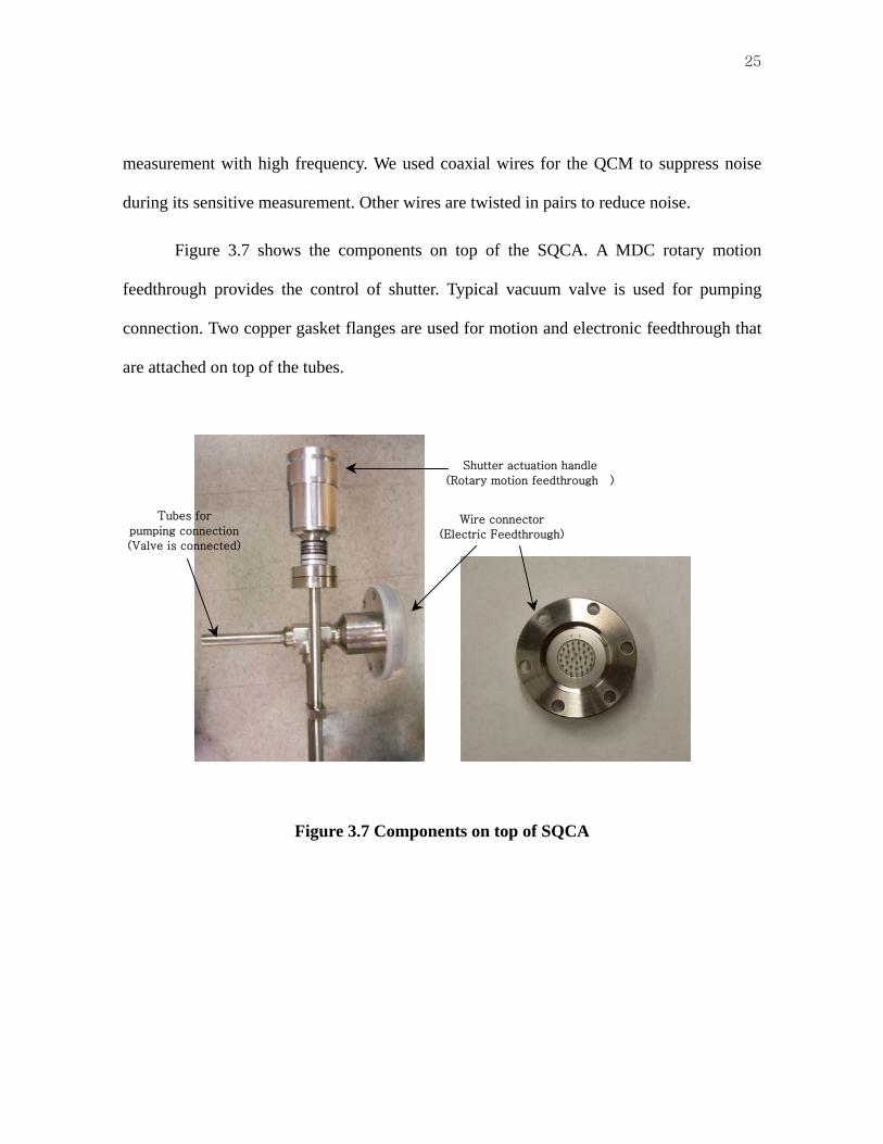
Figure 3.7 shows the components on top of the SQCA. A MDC rotary motion
feedthrough provides the control of shutter. Typical vacuum valve is used for pumping
connection. Two copper gasket flanges are used for motion and electronic feedthrough that
are attached on top of the tubes.
Tubes for
pumping connection
(Valve is connected)
Shutter actuation handle
(Electric Feedthrough)
Wire connector
(Rotary motion feedthrough )
Figure 3.7 Components on top of SQCA
26
CHAPTER IV
EXPERIMENTAL ISSUES
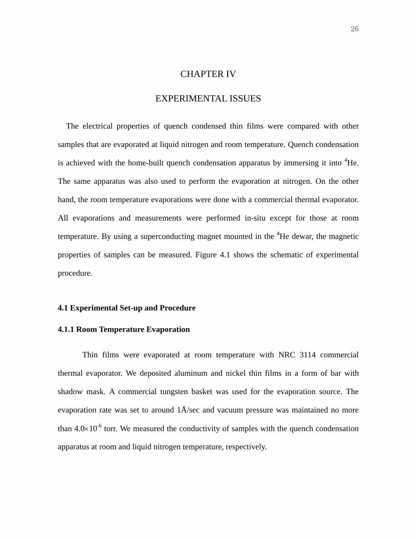
The electrical properties of quench condensed thin films were compared with other
samples that are evaporated at liquid nitrogen and room temperature. Quench condensation
is achieved with the home-built quench condensation apparatus by immersing it into 4He.
The same apparatus was also used to perform the evaporation at nitrogen. On the other
hand, the room temperature evaporations were done with a commercial thermal evaporator.
All evaporations and measurements were performed in-situ except for those at room
temperature. By using a superconducting magnet mounted in the 4He dewar, the magnetic
properties of samples can be measured. Figure 4.1 shows the schematic of experimental
procedure.
4.1 Experimental Set-up and Procedure
4.1.1 Room Temperature Evaporation
Thin films were evaporated at room temperature with NRC 3114 commercial
thermal evaporator. We deposited aluminum and nickel thin films in a form of bar with
shadow mask. A commercial tungsten basket was used for the evaporation source. The
evaporation rate was set to around 1Å/sec and vacuum pressure was maintained no more
than 4.0×10⁻⁶ torr. We measured the conductivity of samples with the quench condensation
apparatus at room and liquid nitrogen temperature, respectively.
27
Evaporation at room
temperature
Sample mounting &
Continuity check of wires
Leaking Test &
Vacuum pumping
System Cooling
(~77K)
Evaporation
Measurement of sample
System Cooling
(~4.2K)
Measurement of sample
(magnetic properties) Room temperature
experiment
Liquid nitrogen experiment
Quench-condensation
In-situ measurement
Figure 4.1 Schematic of experimental procedure
4.1.2 Evaporation at Liquid Nitrogen
The substrate was prepared for in-situ measurements. Before producing a high
vacuum, the vacuum chamber was leak-tested with an Alcatel ASM 142 leak detector. The
chamber was evacuated by using a defunct MS-9 Veeco leak detector which has a rough
and a diffusion pump. To protect the vacuum system, two successive pumping steps were
performed to reach no more than ~10-2 torr at first with the rough pump and then a typical
limit of 10-6 torr with a diffusion pump respectively.
28
The electronic apparatus was connected to the quench-condensation apparatus
before being immersed into a dewar. Two differential preamplifier (PARTM MODEL 116,
117) and two multimeter (HEWLETT PACKARD 3457A, 3478A) were used for the 4-wire
measurement of the sample and thermometer (Cernox CX-1050 thin film resistance sensor).
A precision voltmeter (Guideline 9578) was used as an auxiliary apparatus for the
measurement. A universal counter (HP 5315A) was used to measure the frequency of QCM
for monitoring the thickness of the sample. A stabilized power supply (FARNELL
INSTRUMENT L30-2) and a home made QCM oscillator were used to generate
oscillations on the QCM. The frequency of the QCM and the initial resistance of
thermometer were measured before immersing the apparatus into the dewar.
The vacuum pump was disconnected before immerse the apparatus into liquid nitrogen.
The apparatus was cooled down to 77K over a period of ~20 minute to protect the
electronic feedthrough at the bottom of vacuum chamber. An evaporation was performed by
heating the evaporation source with a DC Power Supply (HP 6274B, maximum 60V and
15A). The sample was measured in-situ and then the sequential process of evaporation and
measurement was repeated.
4.1.3 Quench-Condensation (at 4He)
For a quench-condensation, there are additional processes required for evaporation.
All of the processes were the same compared to liquid nitrogen temperature evaporation
until immersing the apparatus into the dewar. However, the main difference is that, inside
the dewar, the liquid nitrogen has been replaced by 4He. After the dewar was cooed down to
29
77K, liquid nitrogen was removed by producing a pressure in the dewar with nitrogen gas
and then 4He was transferred. During this process, the 4He level was monitored by
measuring the resistance of superconducting wire installed inside of the dewar. A sample
was evaporated when the apparatus reached the temperature of 4.2K. The measurement of
its electrical properties was performed. In addition, the magnetic properties of the sample
were measured by using a superconducting magnet which is installed at the bottom of the
dewar.
4.2 Evaporation Source
It is very important choosing a suitable evaporation source to produce a high quality
sample. To provide good conditions for evaporation, the source must support a material to
evaporate at high temperature without allowing a chemical reaction or significant alloying
between them. The appropriate value of electric current plays a critical role for the success
of an evaporation. It determines the evaporation rate which affects the quality of the sample.
Furthermore, the evaporation is influenced by both the shape and amount of material.
There are different types of evaporation sources for various purposes in thermal
evaporation. Typical evaporation sources are made of the tungsten (W), tantalum (Ta),
molybdenum (Mo) or carbon (C). Tungsten is the most typical source for thermal
evaporation since it has the highest melting point (3695K) and the lowest vapor pressure
[15]. This source, which has a low thermal expansion rate at high temperature, does not
easily oxidize or alloy with other materials. Its resistivity is not larger than that of other
evaporation sources, but increases with temperature. At room temperature, its resistivity is
30
about 5.65 μΩ/cm where as it is 24.93 μΩ/cm at 1000K.
As mentioned before, the geometrical form of an evaporation source affects the
evaporation process. The typical form is a basket, wire coil, boat, crucible, and so on. The
basket is commonly used to evaporate two different kinds of materials, which are non-
adhesive in solid state and adhesive in liquid state. For evaporating non-adhesive materials
or expansive materials, the boat is recommended. The crucible is for large quantities or
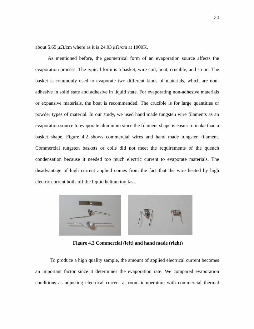
powder types of material. In our study, we used hand made tungsten wire filaments as an
evaporation source to evaporate aluminum since the filament shape is easier to make than a
basket shape. Figure 4.2 shows commercial wires and hand made tungsten filament.
Commercial tungsten baskets or coils did not meet the requirements of the quench
condensation because it needed too much electric current to evaporate materials. The
disadvantage of high current applied comes from the fact that the wire heated by high
electric current boils off the liquid helium too fast.
Figure 4.2 Commercial (left) and hand made (right)
To produce a high quality sample, the amount of applied electrical current becomes
an important factor since it determines the evaporation rate. We compared evaporation
conditions as adjusting electrical current at room temperature with commercial thermal
31
evaporator. This test allows us to learn how much current is needed for evaporation with the
quench-condensation apparatus. Aluminum has been melted for 30 seconds when we
applied electrical current of 30A with commercial evaporator. It was completely melted
several seconds after the start and the evaporation rate was very large (~20 Hz/sec).
Aluminum has started to melt in ~3 minutes with 20A and it completely melted in 30
seconds after start to melt. The evaporation rate was about 6Hz/sec. It takes a long time
(7~8 minutes) at 15A. It did not thoroughly melt before the evaporation. The aluminum
started to evaporate even if it was not thoroughly melted but just partly melted at its
surface. The evaporation rate was about 1~2 Hz/sec. Aluminum did not melt even after
more than 20 minutes and did not evaporated for less than 15A. The frequency of the QCM
has been increased due to the thermal radiation of the evaporation source heated for a long
period. The resonance frequency of the QCM was very unstable and finally it started to
fluctuate after 20 minutes. The resonance frequency of the QCM has increased more than
20 Hz and fluctuated between 10Hz of different values. Table 4.1 shows the instability of
the resonance frequency of QCM.
Table 4.1 The resonance frequency of QCM for the current of less than 15A
Initial value After 5 minutes After 10 minutes After 15 minutes 16~20 minutes
4.984625 MHz 4.984627 MHz 4.984630 MHz 4.984634 MHz 4.984636~45 MHz
(Fluctuating)
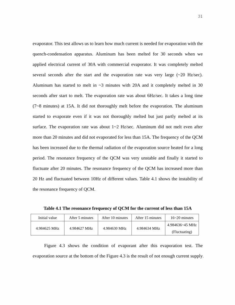
Figure 4.3 shows the condition of evaporant after this evaporation test. The
evaporation source at the bottom of the Figure 4.3 is the result of not enough current supply.
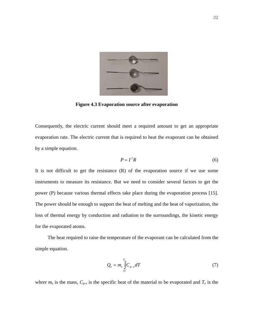
32
Figure 4.3 Evaporation source after evaporation
Consequently, the electric current should meet a required amount to get an appropriate
evaporation rate. The electric current that is required to heat the evaporant can be obtained
by a simple equation.
RIP 2= (6)
It is not difficult to get the resistance (R) of the evaporation source if we use some
instruments to measure its resistance. But we need to consider several factors to get the
power (P) because various thermal effects take place during the evaporation process [15].
The power should be enough to support the heat of melting and the heat of vaporization, the
loss of thermal energy by conduction and radiation to the surroundings, the kinetic energy
for the evaporated atoms.
The heat required to raise the temperature of the evaporant can be calculated from the
simple equation.
dTCmQeT
Tiepee ∫ −= (7)
whrer me is the mass, Cp-e is the specific heat of the material to be evaporated and Te is the
33
temperature at the melting point, Ti is the initial temperature of the material.
The heat for the evaporation source is can be obtained from a similar equation
(8) ∫ −=e
i
T
Tspss dTCmQ
where ms is the mass and Cp-s is the specific heat of the evaporation source.
The latent heat(Ql) is also required so the total required heat can be obtained by
lesetot QmQQQ ++= (9)
We can get the power from these equations with the assumption of that there are no loss of
heats by conduction and radiation.
TR
QRPI tot
Δ== (10)
where ΔT is the time to evaporate all materials to be evaporated. But this is not an exact
current for the evaporation because we neglected the loss of heats. We can roughly derive
the equation for the heat loss by conduction from Fourier’s law.
∫ ⋅Δ−=∂∂
s
c dSTkt
Q (11)
where Qc is the amount of heat conducted, t is the time taken, k is the conductivity of
materials, S is the surface through which the heat is flowing.
We can rewrite this as
dxdTkAQc 2−= (12)
where A is the cross sectional area of the electrodes holding the evaporation source.
The loss of heat by the thermal radiation also needs to be calculated and it can be
done by the Stefan Boltzmann’s Law
34
4TSW ⋅⋅=σ (13)
If we assume that the temperature of the evaporation source is uniform then the thermal
radiation can be roughly calculated as
)( 04 TTlAW ss −= σ (14)
where As is the cross sectional area and l is the length, Ts is the temperature of the
evaporation source.
The total power required for evaporation can be obtained from equations (9, 12, 13)
WQt
QP ctot
tot ++Δ
= (15)
The electric current that is required is
RPI tot= (16)
35
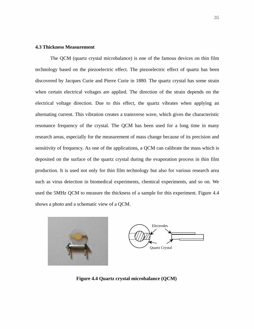
4.3 Thickness Measurement
The QCM (quartz crystal microbalance) is one of the famous devices on thin film
technology based on the piezoelectric effect. The piezoelectric effect of quartz has been
discovered by Jacques Curie and Pierre Curie in 1880. The quartz crystal has some strain
when certain electrical voltages are applied. The direction of the strain depends on the
electrical voltage direction. Due to this effect, the quartz vibrates when applying an
alternating current. This vibration creates a transverse wave, which gives the characteristic
resonance frequency of the crystal. The QCM has been used for a long time in many
research areas, especially for the measurement of mass change because of its precision and
sensitivity of frequency. As one of the applications, a QCM can calibrate the mass which is
deposited on the surface of the quartz crystal during the evaporation process in thin film
production. It is used not only for thin film technology but also for various research area
such as virus detection in biomedical experiments, chemical experiments, and so on. We
used the 5MHz QCM to measure the thickness of a sample for this experiment. Figure 4.4
shows a photo and a schematic view of a QCM.
Electrodes
Quartz Crystal
Figure 4.4 Quartz crystal microbalance (QCM)
36
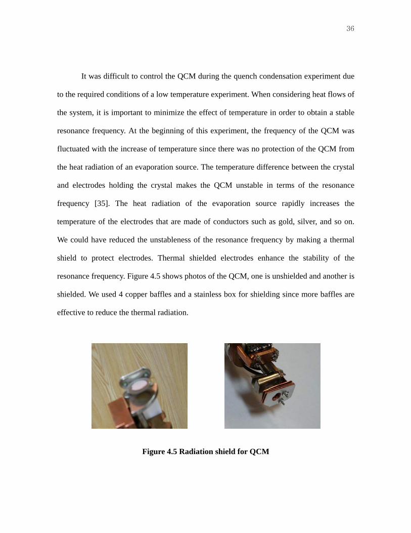
It was difficult to control the QCM during the quench condensation experiment due
to the required conditions of a low temperature experiment. When considering heat flows of
the system, it is important to minimize the effect of temperature in order to obtain a stable
resonance frequency. At the beginning of this experiment, the frequency of the QCM was
fluctuated with the increase of temperature since there was no protection of the QCM from
the heat radiation of an evaporation source. The temperature difference between the crystal
and electrodes holding the crystal makes the QCM unstable in terms of the resonance
frequency [35]. The heat radiation of the evaporation source rapidly increases the
temperature of the electrodes that are made of conductors such as gold, silver, and so on.
We could have reduced the unstableness of the resonance frequency by making a thermal
shield to protect electrodes. Thermal shielded electrodes enhance the stability of the
resonance frequency. Figure 4.5 shows photos of the QCM, one is unshielded and another is
shielded. We used 4 copper baffles and a stainless box for shielding since more baffles are
effective to reduce the thermal radiation.
Figure 4.5 Radiation shield for QCM
37
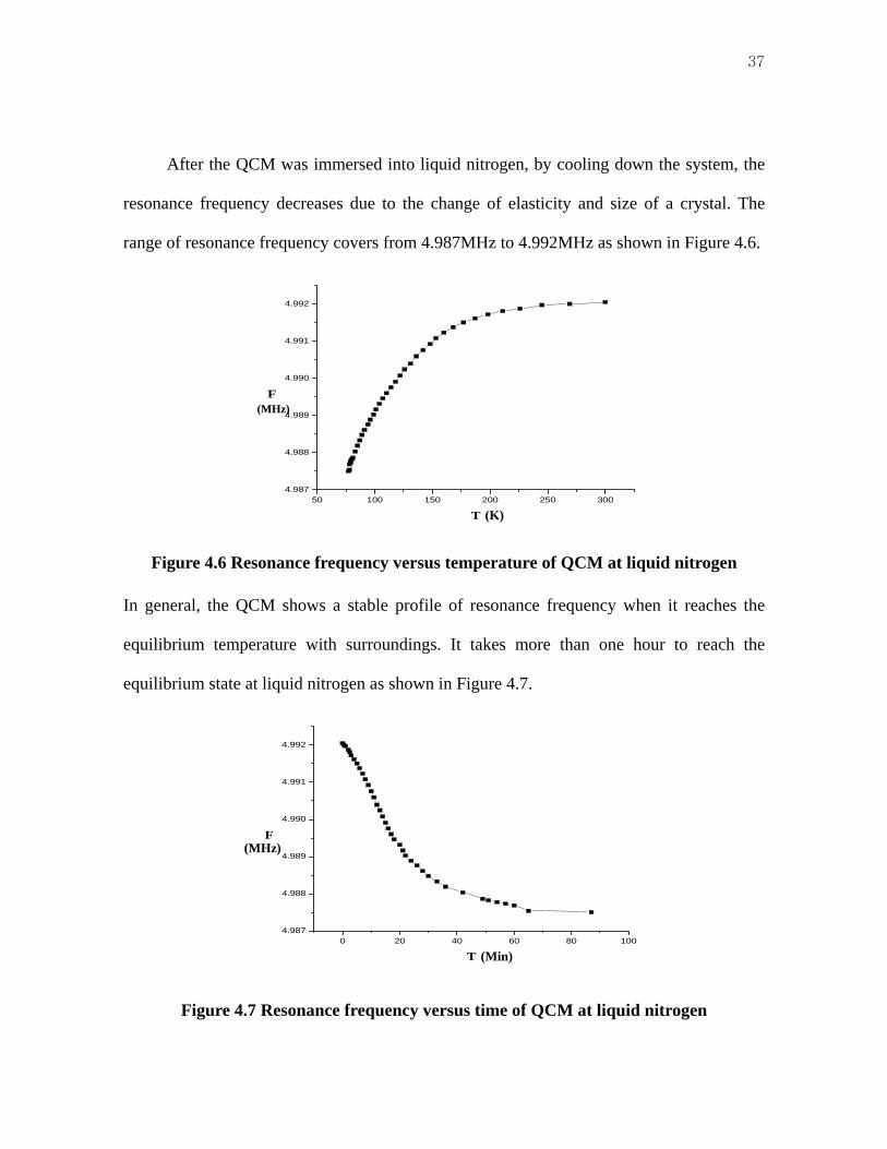
After the QCM was immersed into liquid nitrogen, by cooling down the system, the
resonance frequency decreases due to the change of elasticity and size of a crystal. The
range of resonance frequency covers from 4.987MHz to 4.992MHz as shown in Figure 4.6.
50 100 150 200 250 3004.987
4.988
4.989
4.990
4.991
4.992
F
T
989
4.990
4.991
4.992
(K)
(MHz)
Figure 4.6 Resonance frequency versus temperature of QCM at liquid nitrogen
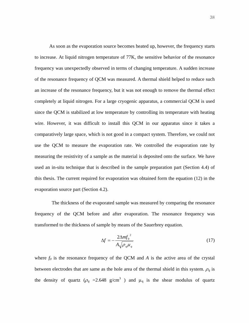
In general, the QCM shows a stable profile of resonance frequency when it reaches the
equilibrium temperature with surroundings. It takes more than one hour to reach the
equilibrium state at liquid nitrogen as shown in Figure 4.7.
0 20 40 60 80 1004.987
4.988
4.
F
T
(MHz)
(Min)
Figure 4.7 Resonance frequency versus time of QCM at liquid nitrogen
38
As soon as the evaporation source becomes heated up, however, the frequency starts
to increase. At liquid nitrogen temperature of 77K, the sensitive behavior of the resonance
frequency was unexpectedly observed in terms of changing temperature. A sudden increase
of the resonance frequency of QCM was measured. A thermal shield helped to reduce such
an increase of the resonance frequency, but it was not enough to remove the thermal effect
completely at liquid nitrogen. For a large cryogenic apparatus, a commercial QCM is used
since the QCM is stabilized at low temperature by controlling its temperature with heating
wire. However, it was difficult to install this QCM in our apparatus since it takes a
comparatively large space, which is not good in a compact system. Therefore, we could not
use the QCM to measure the evaporation rate. We controlled the evaporation rate by
measuring the resistivity of a sample as the material is deposited onto the surface. We have
used an in-situ technique that is described in the sample preparation part (Section 4.4) of
this thesis. The current required for evaporation was obtained form the equation (12) in the
evaporation source part (Section 4.2).
The thickness of the evaporated sample was measured by comparing the resonance
frequency of the QCM before and after evaporation. The resonance frequency was
transformed to the thickness of sample by means of the Sauerbrey equation.
qqA
mff
μρ
202Δ
−=Δ (17)
where f0 is the resonance frequency of the QCM and A is the active area of the crystal
between electrodes that are same as the hole area of the thermal shield in this system. ρq is
the density of quartz (ρq =2.648 g/cm3 ) and μq is the shear modulus of quartz
39
(μq=2.94731011 g/cm3S2)
The mass of deposited materials can be expected from the equation (17) as
20
5103.4f
fAm Δ×≈Δ (18)
Our QCM has a resonance frequency of 5MHz and the active area of the crystal is 0.25cm2.
So the mass change for 1Hz of frequency change is 4.3×10⁻⁹g. The thickness of deposited
material can be calculated from the following relationship
mmA
mtρρ1107.1 8 ××=
Δ= − (19)
where ρm is the density of the deposited material. When changing the thickness by (a
increase of) 1Å, decrease of the resonance frequency for aluminum (ρ = 2.7 g.cm-3) is
1.58Hz/Å and for nickel (ρ = 8.908 g.cm-3) is 5.26 Hz/Å. It is noted that there is 1.3 cm of
gap between the QCM and the substrate of our instrument, which may cause errors in our
measurements. The correction can be made by using the density of the deposition flux.
Assuming that sample is evaporated isotropically from the evaporation source, there is the
relation
(20) 221122 44 mRmR Δ=Δ ππ
where Δm1 is the mass change of QCM and Δm2 is the adjusted mass change.
22
21
12 RRmm Δ=Δ (21)
The corrected thickness can be extracted form the equations (19) and (21) as follows
m
tρ1101.1 8 ××= − (22)
As a result, with increasing thickness of 1Å, decrease of the resonance frequency for
aluminum is 2.4Hz/Å and for nickel is 8.0Hz/Å.
40
4.4 Sample Measurement
We measured the thickness dependent conductivity by means of quench-condensation.
We did 4-wire measurements for samples that are evaporated on glass or silicon substrate.
The measurements are performed in-situ at ultra-high vacuum condition. Sequential
evaporation was performed after measuring the conductivity of a sample at a thickness. The
process is repeated until the thin film shows metallic properties.
For measurement of the thickness dependent conductivity, an in-situ experimental
technique is much more convenient than ex-situ technique. The reason is that the ex-situ
technique requires the fabrication of many samples with different thickness for measuring
the thickness-dependency of conductivity. Beside, it is almost impossible to measure the
electrical property of ultra thin film by using ex-situ technique because the sample loses its
electrical property when ultra thin films are exposed to air. Ex-situ, grains of the thin film
start to coalesce and form large islands which are disconnected by heating to room
temperature, and then the conductivity reduces to zero. Thin films start to oxidize as well if
exposed to the air. Thus, ex-situ treatment causes irreversible changes in the topology of
ultra thin films and significantly changes their electrical property. On the other hand, it was
convenient for us to measure the thickness-dependent conductivity of ultra thin films with
in-situ experiment. For in-situ treatment, the sample does not experience any critical change
of electrical property.
We prepared 4 thin gold contacts on a substrate for in-situ measurement by using a
commercial thermal evaporator. 3nm of germanium was deposited on silicon or glass
substrate and then 20nm of gold was deposited by using shadow mask. Germanium was
41
evaporated because gold does not readily adhere on the silicon or glass substrate. We used
two kinds of substrates (silicon and glass) because the thin film has different electrical
property depending on the choice of substrate. The uniformity of the thin film, depending
on the nature of substrate, results in the modification of electrical property by different
choices of substrate. The thin film has different grain sizes, which causes the different
electrical properties of the thin film. Wires are connected to gold contacts before evacuating
the chamber and then a shadow mask was mounted on the substrate to make a sample in the
form of a bar.
Initially a film is evaporated until the conduction is measured. We performed 2-wire
measurements with a precision voltmeter until measuring the initial conduction, and then
performed a 4-wire measurement. The order of measurement is important to check whether
or not the sample initially has infinite resistance that would impose an overload for
differential preamplifier. During evaporation, the temperature of the substrate increased by
~10K. Measurement of resistance was performed while cooling down the sample to its
initial temperature, and then an evaporation was performed again after the sample had
uniform resistance. We repeated the sequential process until the thin film had a certain
resistance. Figure 4.8 shows schematics of the process.
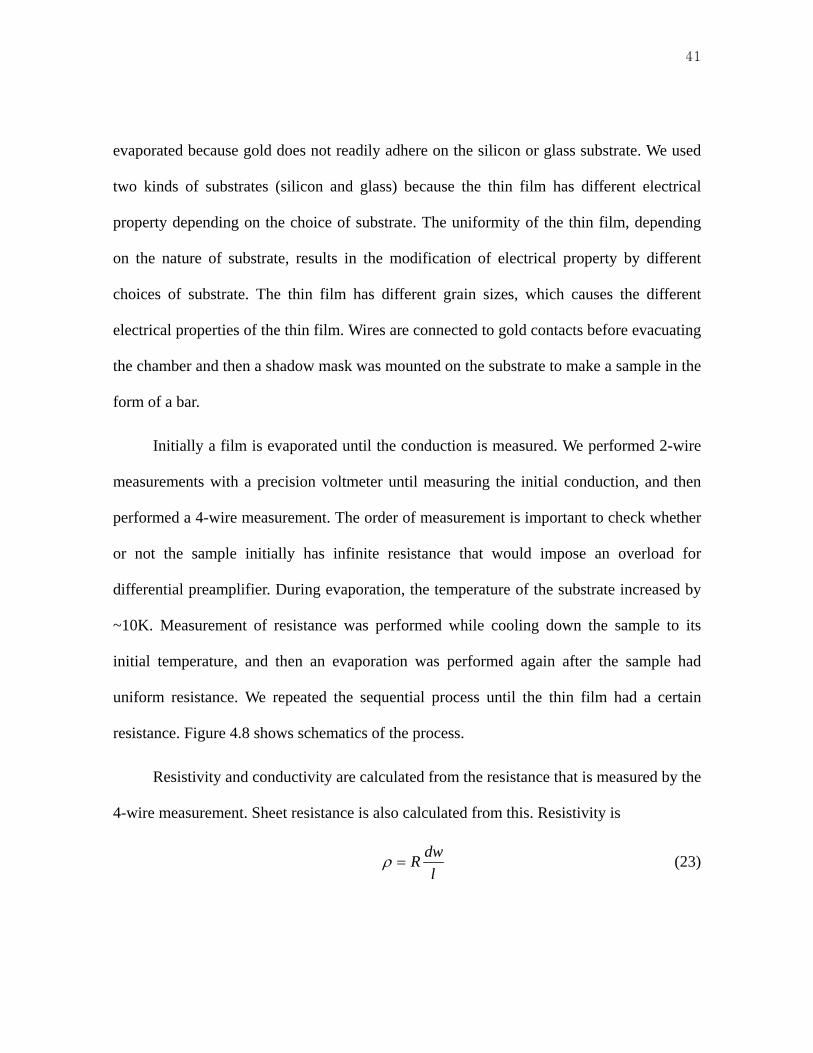
Resistivity and conductivity are calculated from the resistance that is measured by the
4-wire measurement. Sheet resistance is also calculated from this. Resistivity is
l
dwR=ρ (23)
42
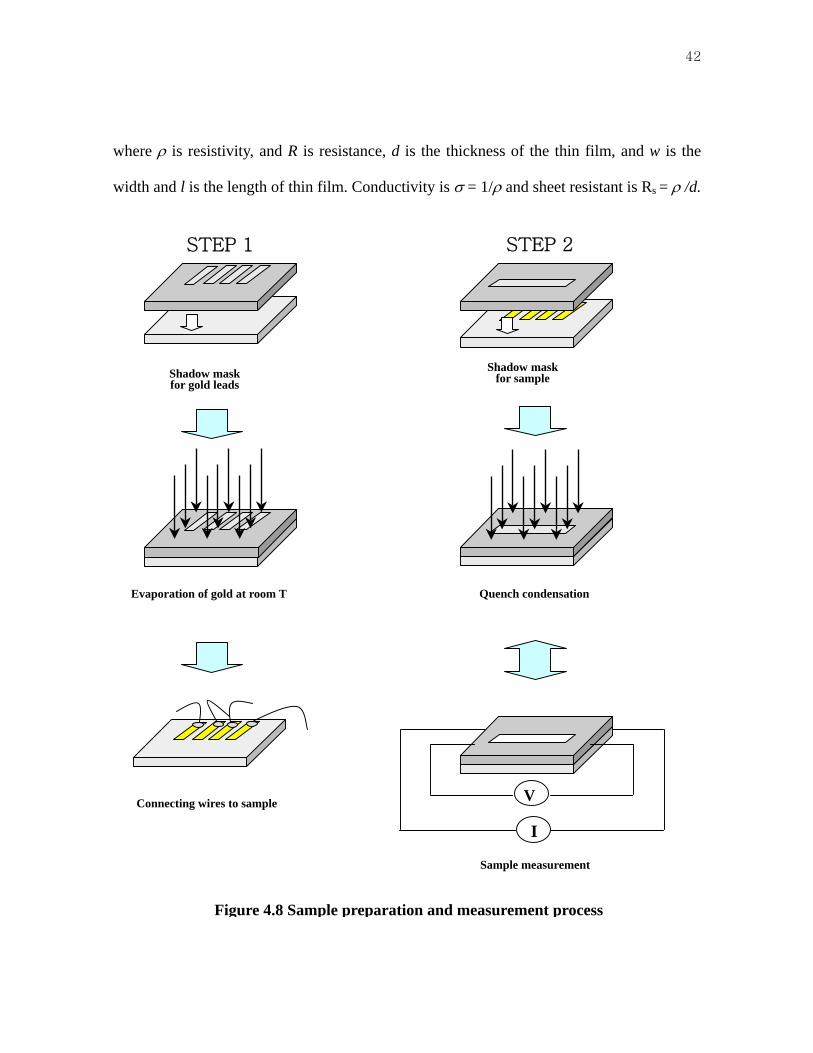
where ρ is resistivity, and R is resistance, d is the thickness of the thin film, and w is the
width and l is the length of thin film. Conductivity is σ = 1/ρ and sheet resistant is Rs = ρ /d.
Shadow mask for sample
Quench condensation
V
I
Sample measurement
STEP 1 STEP 2
Shadow mask for gold leads
Evaporation of gold at room T
Connecting wires to sample
Figure 4.8 Sample preparation and measurement process
43
CHAPTER V
EXPERIMENTAL RESULTS AND DISCUSSION
5.1 Experimental Results
5.1.1 Evaporation of Aluminum at Liquid Nitrogen
Aluminum thin films were deposited onto a silicon substrate and a glass substrate at
77°K. Sequential evaporations and in-situ measurements were performed with the quench
condensation apparatus. The temperature of the substrate was maintained at 77K before and
after the evaporation but it rose to ∼86K during the evaporation. A vacuum was always
maintained during the experiment.
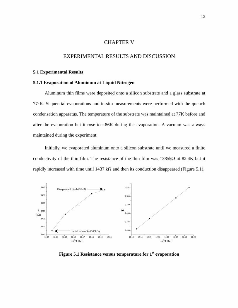
Initially, we evaporated aluminum onto a silicon substrate until we measured a finite
conductivity of the thin film. The resistance of the thin film was 1385kΩ at 82.4K but it
rapidly increased with time until 1437 kΩ and then its conduction disappeared (Figure 5.1).
12.13 12.14 12.15 12.16 12.17 12.18 12.19 12.201380
1390
1400
1410
1420
1430
1440
R
12.13 12.14 12.15 12.16 12.17 12.18 12.19 12.20
2.496
2.497
2.498
2.499
2.500
2.501
lnR
Initial value (R=1385kΩ)
Disappeared (R=1437kΩ)
(kΩ)
103/T (K-1) 103/T (K-1)
Figure 5.1 Resistance versus temperature for 1st evaporation
44
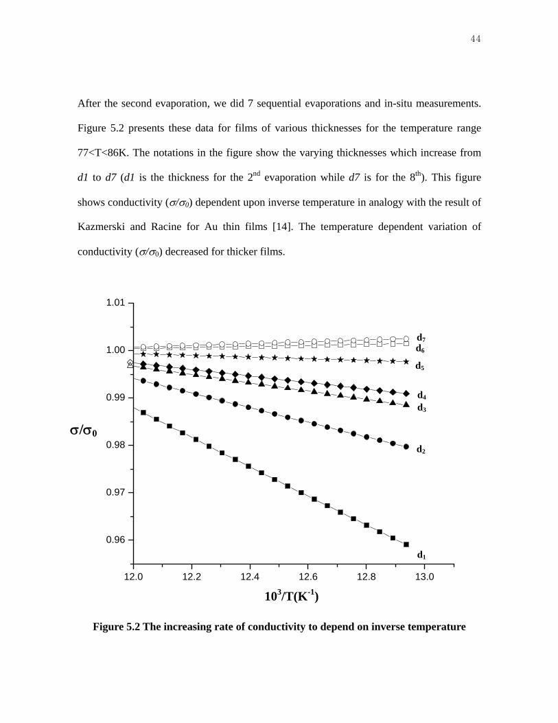
After the second evaporation, we did 7 sequential evaporations and in-situ measurements.
Figure 5.2 presents these data for films of various thicknesses for the temperature range
77<T<86K. The notations in the figure show the varying thicknesses which increase from
d1 to d7 (d1 is the thickness for the 2nd evaporation while d7 is for the 8th). This figure
shows conductivity (σ/σ0) dependent upon inverse temperature in analogy with the result of
Kazmerski and Racine for Au thin films [14]. The temperature dependent variation of
conductivity (σ/σ0) decreased for thicker films.
12.0 12.2 12.4 12.6 12.8 13.0
0.96
0.97
0.98
0.99
1.00
1.01
d6
d7
d5
d3
d4
σ/σ0d2
d1
103/T(K-1)
Figure 5.2 The increasing rate of conductivity to depend on inverse temperature
45
11.6 11.8 12.0 12.2 12.4 12.6 12.8 13.0
51.5
52.0
52.5
53.0
53.5
54.0
R
11.6 11.8 12.0 12.2 12.4 12.6 12.8 13.0
684.0
684.2
684.4
684.6
684.8
685.0
R(Ω) (kΩ)
103/T (K-1) 103/T (K-1)
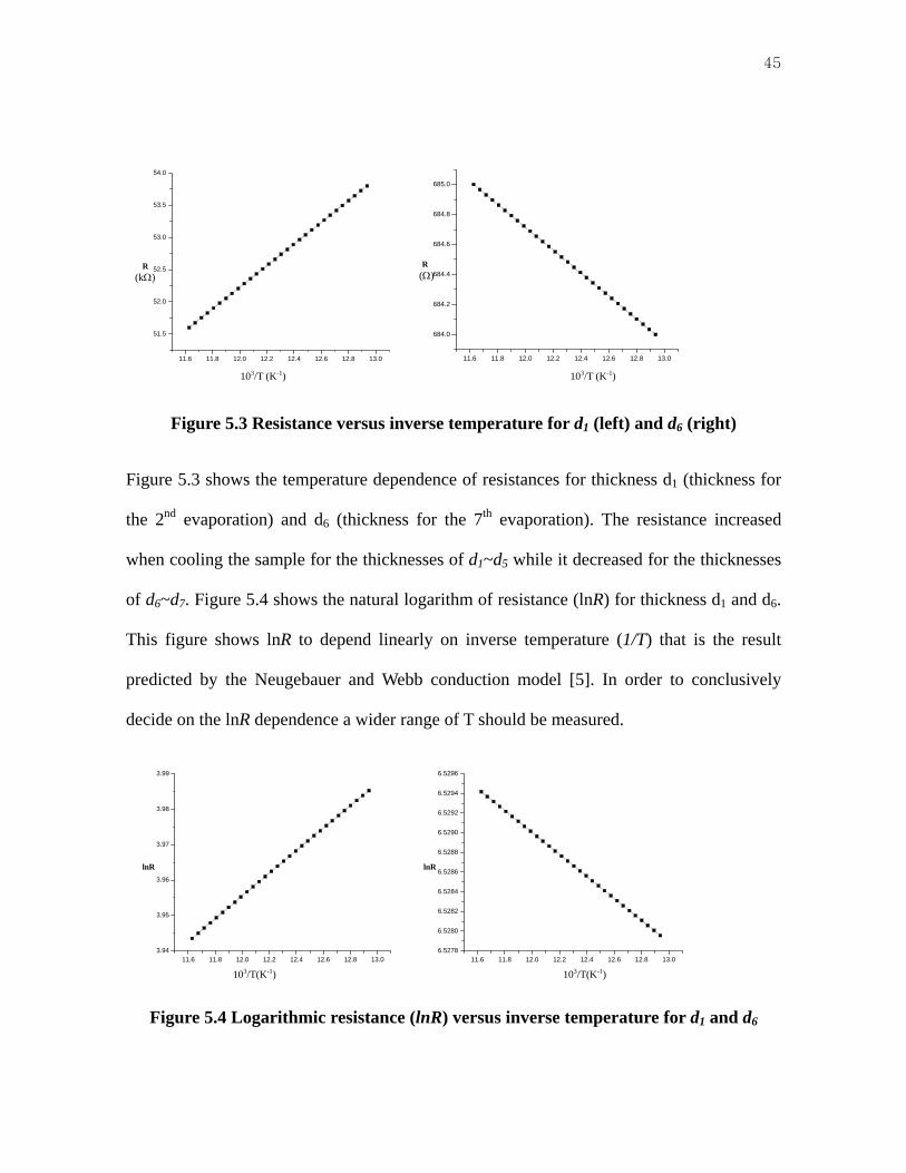
Figure 5.3 Resistance versus inverse temperature for d1 (left) and d6 (right)
Figure 5.3 shows the temperature dependence of resistances for thickness d1 (thickness for
the 2nd evaporation) and d6 (thickness for the 7th evaporation). The resistance increased
when cooling the sample for the thicknesses of d1~d5 while it decreased for the thicknesses
of d6~d7. Figure 5.4 shows the natural logarithm of resistance (lnR) for thickness d1 and d6.
This figure shows lnR to depend linearly on inverse temperature (1/T) that is the result
predicted by the Neugebauer and Webb conduction model [5]. In order to conclusively
decide on the lnR dependence a wider range of T should be measured.
11.6 11.8 12.0 12.2 12.4 12.6 12.8 13.03.94
3.95
3.96
3.97
3.98
3.99
lnR
11.6 11.8 12.0 12.2 12.4 12.6 12.8 13.06.5278
6.5280
6.5282
6.5284
6.5286
6.5288
6.5290
6.5292
6.5294
6.5296
lnR
103/T(K-1) 103/T(K-1)
Figure 5.4 Logarithmic resistance (lnR) versus inverse temperature for d1 and d6
46
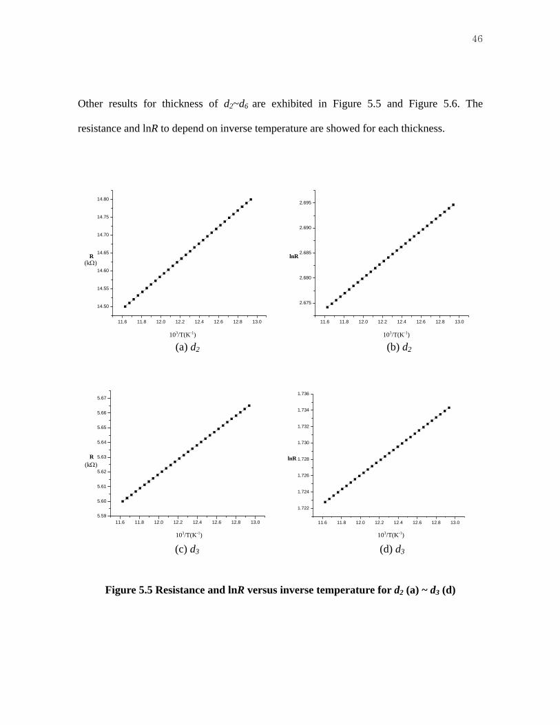
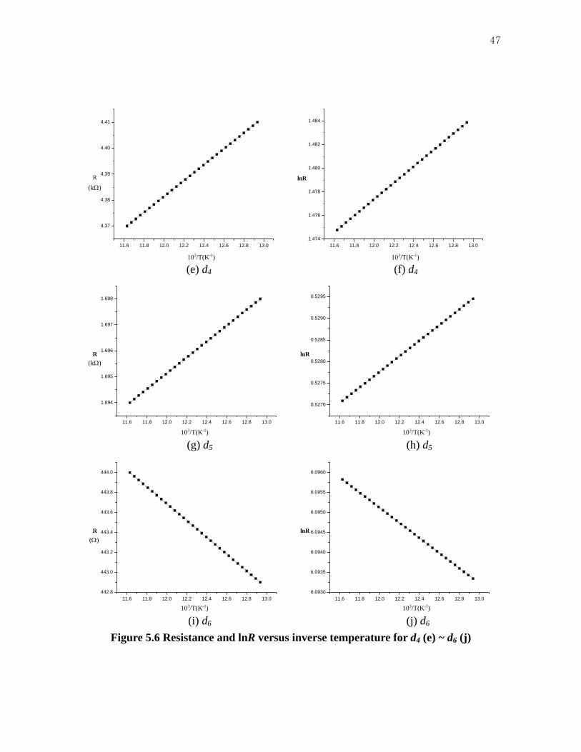
Other results for thickness of d2~d6 are exhibited in Figure 5.5 and Figure 5.6. The
resistance and lnR to depend on inverse temperature are showed for each thickness.
11.6 11.8 12.0 12.2 12.4 12.6 12.8 13.0
14.50
14.55
14.60
14.65
14.70
14.75
14.80
R
11.6 11.8 12.0 12.2 12.4 12.6 12.8 13.0
2.675
2.680
2.685
2.690
2.695
lnR
(kΩ)
103/T(K-1) 103/T(K-1)
(a) d2 (b) d2
11.6 11.8 12.0 12.2 12.4 12.6 12.8 13.05.59
5.60
5.61
5.62
5.63
5.64
5.65
5.66
5.67
R
11.6 11.8 12.0 12.2 12.4 12.6 12.8 13.0
1.722
1.724
1.726
1.728
1.730
1.732
1.734
1.736
lnR
(kΩ)
103/T(K-1) 103/T(K-1)
(c) d3 (d) d3
Figure 5.5 Resistance and lnR versus inverse temperature for d2 (a) ~ d3 (d)
47
11.6 11.8 12.0 12.2 12.4 12.6 12.8 13.0
4.37
4.38
4.39
4.40
4.41
R
11.6 11.8 12.0 12.2 12.4 12.6 12.8 13.01.474
1.476
1.478
1.480
1.482
1.484
lnR
(kΩ)
103/T(K-1)
(e) d4
103/T(K-1)
(f) d4
11.6 11.8 12.0 12.2 12.4 12.6 12.8 13.0
1.694
1.695
1.696
1.697
1.698
R
11.6 11.8 12.0 12.2 12.4 12.6 12.8 13.0
0.5270
0.5275
0.5280
0.5285
0.5290
0.5295
lnR
(kΩ)
103/T(K-1) 103/T(K-1)
(g) d5 (h) d5
11.6 11.8 12.0 12.2 12.4 12.6 12.8 13.0442.8
443.0
443.2
443.4
443.6
443.8
444.0
R
11.6 11.8 12.0 12.2 12.4 12.6 12.8 13.06.0930
6.0935
6.0940
6.0945
6.0950
6.0955
6.0960
lnR
(Ω)
103/T(K-1) 103/T(K-1)
(i) d6 (j) d6
Figure 5.6 Resistance and lnR versus inverse temperature for d4 (e) ~ d6 (j)
48
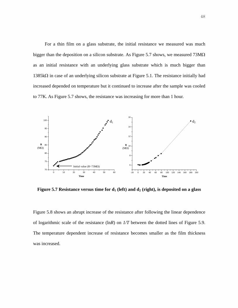
For a thin film on a glass substrate, the initial resistance we measured was much
bigger than the deposition on a silicon substrate. As Figure 5.7 shows, we measured 73MΩ
as an initial resistance with an underlying glass substrate which is much bigger than
1385kΩ in case of an underlying silicon substrate at Figure 5.1. The resistance initially had
increased depended on temperature but it continued to increase after the sample was cooled
to 77K. As Figure 5.7 shows, the resistance was increasing for more than 1 hour.
0 10 20 30 40 50 6070
75
80
85
90
95
100
R
Time-20 0 20 40 60 80 100 120 140 160 180 200
6
8
10
12
14
16
R
Time
d1 d2
(MΩ) (MΩ)
Initial value (R=73MΩ)
Figure 5.7 Resistance versus time for d1 (left) and d2 (right), is deposited on a glass
Figure 5.8 shows an abrupt increase of the resistance after following the linear dependence
of logarithmic scale of the resistance (lnR) on 1/T between the dotted lines of Figure 5.9.
The temperature dependent increase of resistance becomes smaller as the film thickness
was increased.
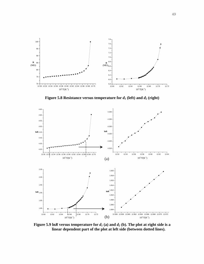
49
12.50 12.52 12.54 12.56 12.58 12.60 12.62 12.64 12.66 12.68 12.7070
75
80
85
90
95
100
R
12.60 12.62 12.64 12.66 12.68 12.70 12.725.8
6.0
6.2
6.4
6.8
7.0
7.2
7.4
7.6
7.8
R(MΩ) 6.6(MΩ)
103/T(K-1) 103/T(K-1)
Figure 5.8 Resistance versus temperature for d1 (left) and d2 (right)
12.50 12.52 12.54 12.56 12.58 12.60 12.62 12.64 12.66 12.68 12.70
4.30
4.35
4.40
4.45
4.50
4.55
4.60
4.65
lnR
12.52 12.54 12.56 12.58 12.60 12.62 12.64
4.315
4.320
4.325
4.330
4.335
4.340
lnR
12.60 12.62 12.64 12.66 12.68 12.70 12.72
1.80
1.85
1.90
1.95
2.00
2.05
lnR
12.656 12.658 12.660 12.662 12.664 12.666 12.668 12.670 12.672
1.804
1.806
1.808
1.810
1.812
1.814
1.816
1.818
1.820
lnR
103/T(K-1)
103/T(K-1) (a) 103/T(K-1)
(b) 103/T(K-1)
Figure 5.9 lnR versus temperature for d1 (a) and d2 (b). The plot at right side is a linear dependent part of the plot at left side (between dotted lines).
50
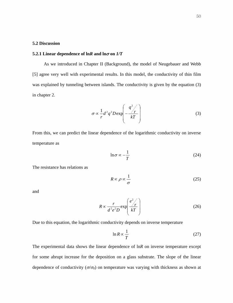
5.2 Discussion
5.2.1 Linear dependence of lnR and lnσ on 1/T
As we introduced in Chapter II (Background), the model of Neugebauer and Webb
[5] agree very well with experimental results. In this model, the conductivity of thin film
was explained by tunneling between islands. The conductivity is given by the equation (3)
in chapter 2.
⎟⎟⎟
⎠
⎞
⎜⎜⎜
⎝
⎛−∝
kTr
qDqd
r
2
22 exp1σ (3)
From this, we can predict the linear dependence of the logarithmic conductivity on inverse
temperature as
T1ln −∝σ (24)
The resistance has relations as
σ
ρ 1∝∝R (25)
and
⎟⎟⎟
⎠
⎞
⎜⎜⎜
⎝
⎛∝
kTr
e
DedrR
2
22 exp (26)
Due to this equation, the logarithmic conductivity depends on inverse temperature
T
R 1ln ∝ (27)
The experimental data shows the linear dependence of lnR on inverse temperature except
for some abrupt increase for the deposition on a glass substrate. The slope of the linear
dependence of conductivity (σ/σ0) on temperature was varying with thickness as shown at
51
Figure 5.2. This can be expected from the equation (26) by modify some parameters as
( )BdrkTA
rdC −= εσ exp)( (28)
where A is a function of e2 and ε is an effective dielectric constant of the media between
islands. C and B are constant which depend on the potential (V) of the tunneling barrier (C,
B ∝ qV). Due to equation (28), the slope of the plots in Figure 5.2 is decreasing with the
thickness of the sample since the exponential terms of the equation becomes constant by
increase of the effective island size r during the growth of the sample. As Figure 5.3 and 5.4
show, the resistance also depends almost linearly on inverse temperature. This is due to the
fact that the temperature range (77 < T < 86K) was too narrow to show the obvious
logarithmic curvature. The preciseness of the temperature calibration can also affect the
curvature.
5.2.2 Initial Value of the Resistance
As Figure 5.1 and 5.7 show, the initial resistance of the deposition on a glass
substrate was different from the deposition on a silicon substrate. This can be explained in
several ways depending on substrates as the saturation ratio, the surface roughness, and
electrical effect of silicon substrate.
(a) Surface roughness
The surface roughness of a substrate results in different growth conditions of a thin
film. Since the surface of a silicon substrate is comparatively smooth and uniform the
aluminum forms a uniform thin film on the silicon substrate. On the other hand, the glass
substrate has a comparatively rough surface unless it has been polished to be smooth. Thus
52
the aluminum forms a rough thin film on the glass substrate. This should increase the inter
island separation (d) and finally increase the resistance of thin film.
(b) Electrical effect of silicon substrate
The silicon has some conductivity (being a semiconductor) while the glass has very
poor conductivity, being an insulator. It is possible that the SiO2 layer of the silicon
substrate was saturated with aluminum during the deposition and formed some mixed layer
on the boundary between the thin film and the substrate. This effect is a task of future work
and will not be discussed in detail. If the aluminum is mixed with the SiO2 layer on the
boundary by saturation then it can affect the conductivity of thin film. The tunneling area
can be changed by variation of the dielectric constant between the grains of the thin film.
More over, the conductivity can be increased by the addition of surface impurities after the
aluminum is mixing with the silicon at the boundary of substrate [36].
5.2.3 Abrupt Increase of the Resistance
As Figure 5.8 shows, an abrupt increase of the resistance during the deposition of
aluminum on the glass substrate. This can be explained by the contamination of the ultra-
thin film and substrate through the adsorption of oxygen at the film surface [14, 36].
Fehlner has described the increase of resistance of zirconium films [37] by oxidation. At a
pressure of 10-7 torr, which is lower than the pressure of our experiment when evaporating
aluminum at liquid nitrogen, the oxygen formed a monolayer on the island of the thin film
and then it increased the resistance sharply. Kazmerski and Racine had a similar
experimental result and explained this with the varying of the effective tunneling distance,
53
which is the same as the inter island separation (d), due to the adsorption of oxygen [14].
As Figure 5.10 shows, oxygen forms a thin monolayer of Al2O3 on the island which
increases the resistance of the thin film by increasing the tunneling barrier between islands.
Increased energyafter oxidation Oxidized monolayer
Substrate
Initial energy
Figure 5.10 Increase of the tunneling barrier by oxidation of thin film
Lazarov and St. Manev have found oxygen absorption by a discontinuous gallium thin film
at 77K.
It is likely that the abrupt increase of resistance of our experimental data is due to the
oxidation of the aluminum thin film. During the deposition of aluminum on the glass
substrate, the vacuum level of the chamber was less than 10-6 and the thin film was left for a
long time (t > 1hour) after evaporation. This was a comparatively long time and aluminum
is comparatively easy to oxidize. Some outgassing may also be produced during the
measurement and then the thin film was oxidized.
It is important to notice that the evaporation at liquid nitrogen is not appropriate for
sequential in-situ experiments on aluminum unless the turn-around time of evaporations
and measurements is very quick. This may similar for the evaporation of nickel. Even if we
54
can get a better quality of thin film from the evaporation at liquid nitrogen than from the
evaporation at room temperature, the quality is limited to a certain level. On the other hand,
the oxidation of a thin film is significantly reduces when quench-condensing at liquid
helium since the system maintains an ultra-high vacuum by cryopumping of the apparatus.
55
CHAPTER VI
CONCLUSION
The growth process and the electrical properties of a thin film were investigated by
using the newly designed apparatus at liquid nitrogen. Especially the dependence of non-
metallic behaviors was investigated by means of the in-situ measurement. The apparatus
has potential to be used for many experiments in the future. Due to its ability to perform in-
situ experiment at low temperature, it was convenient for experimental results on ultra-thin
films.
The temperature was too high to quickly quench-condense the evaporated materials
on the substrate to form a uniform thin film. The vacuum pressure produced by
cryopumping of liquid nitrogen and room temperature pumping with the diffusion pump
was not enough to completely protect the sample from the oxidation during the sequential
evaporations.
Some additional experiments will need to be performed until this experimental
technique is optimized. In the future work, we will investigate the electrical properties of
thin films at liquid helium by applying the quench-condensation technique to fabricate
nickel thin film. Once successful, we will continue to investigate the magnetic field driven
metal-insulator transition.
56
REFERENCES
[1] W. Teizer, F. Hellman, and R. C. Dynes, Phys. Rev. Lett. 85, 848 (2000). [2] W. Teizer, F. Hellman, and R. C. Dynes, Solid State Commun. 114, 81 (2000). [3]. A. Frydman, Physica C 391, 189(2003) [4]. A. Frydman, O. Naaman, and R. C. Dynes, Phys. Rev. B. 66, 052509 (2002) [5]. C. A. Neugebauer and M. B. Webb, J. Appl Phys. 33, 74 (1962) [6] A. A. Milgram and C. S. Lu, J. Appl Phys. 37(13) 4773 (1966) [7] P. Sheng, B. Abeles and Y. Arie, Phys. Rev. Lett. 31, 44 (1973) [8] B. L. Altshulter and A. G. Aronov, P. A. Lee, Phys. Rev. Lett. 44, 1288 (1980) [9] J. K. Graybeal and M. R. Beasley, Phys. Rev. B. 29, 4167 (1984) [10] H. M. Jaeger, D. B. Haviland, B. G. Orr, and A. M. Goldman, Phys. Rev. B. 40, 182
(1989) [11] Matthew P. A. Fisher, Phys. Rev. Lett. 65, 923 (1990) [12] M. Strongin, R. S. Thompshon, O. F. Kammerer and J. E. Crow, Phys. Rev. B. 1, 1078
(1970) [13] G. J. Dolan and D. D. Osheroff, Phys. Rev. Lett. 43, 721 (1979) [14] L. L. Kazmerski and D. M. Racine, J. Appl Phys. 46, 791 (1975) [15] K. S. Sree Harsha, Principles of Physical Vapor Deposition of Thin Films (Elsevier,
Boston, 2006) [16] A. E. Riad and F. D. Barlow III, Thin Film Technology Handbook (McGraw-Hill, New
York, 1997) [17] D. G. Naugle, B. Bandyopdhyay, Yin Bo, V. M. Nicoli, R. C. Wang, and D. Rathnayaka,
Rev. Sci. Instrum. 58, 1271 (1987) [18] L. M. Hernandez and A. M. Goldman, Rev. Rev. Sci. Instrum. 73, 162 (2002) [19] M. Curry, D. Arrington and S. C. Street, J. Vac. Sci. Technol. A 21(1), 234 (2003) [20] M. Zinke-Allmang, L. C. Feldamn, S. Nakahara, and B. A. Davidson, Phys. Rev. B. 38,
7848 (1989) [21] A. Raab and G. Springholz, Appl. Phys. Lett. 77, 2991 (2000) [22] R. C. Dynes, J. P. Garno, and J. M. Rowell, Phys. Rev. Lett. 40, 479 (1978) [23] B. G. Chae, H. T. Kim, S. J. Yun, B. J. Kim, Y. W. Lee, and K. Y. Kang, J. J. App. Phys.
46, 738 (2007) [24] N. F. Mott, Rev. Mod. Phys.40, 677 (1968)
57
[25] F. Gebhard, The Mott Metal-Insulator Transition (Springer Berlin, Heidelberg, 2000) [26] D. J. Scalapino, S. R. White and S. Zhang, Phys. Rev. B. 47, 7995 (1993) [27] M. Oshikawa, Phys. Rev. Lett. 90, 236401 (2003) [28] T. Ihn, Electronic Quantum Transport in Mesoscopic Semiconductor (Springer Berlin,
Heidelberg, 2004) [29] E. I. Zornberg, Phys. Rev. B. 1, 244 (1970) [30] G. S. Painter, D. E. Ellis and A. R. Lubinsky, Phys. Rev. B. 4, 3610 (1971) [31] N. F. Mott, Metal-Insulator Transition (Taylor & Francis Ltd, New York, 1974) [32] E. D. Black and John C. Price, Phys. Rev. B 58, 7844 (1998) [33] R. C. Richardson and E. N. Smith, Experimental Techniques in Condensed Matter
Physics at Low Temperatures (Addision-Wesley, Redwood City, CA, 1988) [34] G. K. White and P. J. Meeson, Experimental Techniques in Low-Temperature Physics
(Oxford University Press, Oxford, 2002) [35] L. Bouzidi, S. S. Narine, K. G. Stefanov, and A. J. Slavin, Rev. Sci. Instrum. 74, 3039
(2003) [36] J. E. Morris and T. J. Coutts, Thin Solid Films. 47, 3 (1977) [37] F. P. Fehlner, Nature. 210, 1035 (1966)
58
VITA
Kyoungjin Lee was born in 1978 in SeongNam, The Republic of Korea. He received
a B.S. in applied physics from the Korea Military Academy in 2001, then he was
commissioned as a Artillery officer. He served in the ROK Army from 2001 to 2004 as a
fire battery leader and staff officer. He entered the Physics Department at Texas A&M
University in 2005 as an M.S. student and graduated in August 2007.
Permanent Address: 73-1 Hyeonbang-Ri Baeksa-Myon Ichen, Gyonggi-Do, 467-830, Republic of Korea.
E-mail Address: [email protected]