Embed Size (px)
Citation preview

International Journal of Latest Research In Engineering and Computing (IJLREC) Volume 1, Issue 1 : Page No.84-95, September-October 2013 www.ijlrec.com
Copyright © IJLREC 84
Electrical Interconnections Limits and Optical Interconnections Solutions to Signal Propagation
delay for On Chip Data Path
Ahmed Nabih Zaki Rashed
Electronics and Electrical Communications Engineering Department Faculty of Electronic Engineering, Menouf 32951, Menoufia University, EGYPT
Abstract: Optical interconnection is a promising solution for high speed interconnects between chips or boards to solve the inherent limits of electrical interconnects in speed, crosstalk, and power dissipation. It is believed that the concept of integrated optical interconnect is a potential technological solution to alleviate some of the ever more pressing issues involved in exchanging data between cores in optical communication architectures (inter-line crosstalk, latency, connectivity and power consumption). This paper has presented optical interconnects that bring advantage of high data rate density, i.e. large bandwidth with small physical dimensions, as well as large bandwidth x distance product. High data rate density enables tight integration of many optical channels with electronic chips.
Keywords: Semiconductor technology, Optical interconnections, optical backplane, On chip, active and passive components.
INTRODUCTION Increasing interchip communication bandwidth demand has motivated investigation into using optical interconnect architectures over channel limited electrical counterparts. Optical interconnects with negligible frequency dependent loss and high bandwidth [1] provide a viable alternative to achieve dramatic power efficiency improvements at per channel data rates exceeding 10 Gb/s. This has motivated extensive research into optical interconnect technologies suitable for high density integration with CMOS chips. Directly modulated lasers and optical modulators, both electroabsorption and refractive, have been proposed as high bandwidth optical sources, with these different sources displaying tradeoffs in both device and circuit driver efficiency. Vertical-cavity surface-emitting lasers (VCSELs) [2] are an attractive candidate due to their ability to directly emit light with low threshold currents and reasonable slope efficiency values; however, their speed is limited by both electrical parasitics and carrier photon interactions. A device that does not display this carrier speed limitation is the electroabsorption modulator (EAM), based on either the quantum confined Stark effect [3] or the Franz Keldysh effect [4], which is capable of achieving acceptable contrast ratios (CRs) at low drive voltages over tens of nanometers of optical bandwidth. Ring resonator modulators [5], [6] are refractive devices that display very high resonant quality factors and can achieve high CRs with small dimensions and low capacitance; however, their optical bandwidth is typically less than 1 nm. Another refractive device capable of wide optical bandwidth (> 100 nm) is the Mach Zehnder modulator (MZM) [7]; however, this comes at the cost of a large device and high voltage swings. All of the optical modulators also require an external source laser and incur additional coupling losses relative to a VCSEL-based link. Photodetector (PD) efficiency plays a key role in setting the maximum data rate and tolerable channel loss. High speed p-i-n photodiodes [8] are commonly used in optical receivers due to their high responsivity and low capacitance, whereas emerging ultra low capacitance waveguide PDs [9] integrated with CMOS receivers have the potential to dramatically improve optical receiver efficiency. Requirements for interconnects in computing systems are getting harder to satisfy without employing optical technologies, as the performance keeps growing with the evolution of CMOS technologies as well as system architectures. The emphasis of system designs has been shifting toward reducing power consumption from increasing performance [10]. The total system power, including the power required for cooling as well as for computation, is reaching to or even exceeding the limit of power supply when the system performance is increased. One main advantage of optical compared to electrical interconnects, in addition to the benefit of long-distance transmission at high data rate with optics, is a high data rate density, which provides large bandwidth through a small volume or area. This results in an efficient flow of cooling air through systems as well as tight integration of optical interconnects with electronic chips. As the bandwidth and channel count of interconnects has to be increased for evolving system performance and architecture, these benefits of optical interconnects are crucial [11]. In the present study, different electrical and optical interconnections have been investigated under the same interconnection dimensions and ambient temperature variations. Signal propagation delay and data transmission bit rates are the major interesting design parameters for the evaluation between the electrical and optical interconnections performance.
id46460014 pdfMachine by Broadgun Software - a great PDF writer! - a great PDF creator! - http://www.pdfmachine.com http://www.broadgun.com

International Journal of Latest Research in Engineering and Computing, volume 1,Issue 1, September-October 2013
Copyright © IJLREC 85
ON CHIP OPTICAL INTERCONNECTION DATA PATH Introducing optical interconnects into very large scale integrated (VLSI) architectures requires compatibility with CMOS technology. Due to the absence of an efficient silicon-based laser, only those configurations that utilize an external laser as a light source are considered. A diagram of an optical interconnect system is shown in Fig. 1. A transmitter is used to convert an electrical signal to a light signal, which is composed of a modulator and a driver circuit. The development of a fast and cost efficient CMOS compatible electro-optical modulator is one of the most challenging tasks on the path towards realizing on-chip optical interconnects [12].
Fig. 1. An on chip optical interconnection data path.
Polymer or silicon-on insulator (SOI) waveguides are used to transmit the optical signal. The optical signal is converted to an electrical signal at the receiver. The receiver has two components: a SiGe metal semiconductor metal (MSM) detector and an amplifier. Models of different components within the optical data path are provided in [13]. Unlike electrical devices, optical devices are not readily scalable due to the light wavelength constraint. The performance and integration ability of optical devices, however, are expected to be further improved by technology innovations and structural optimization.
MATHEMATICAL MODEL ANALYSIS With decreasing device dimensions, we are also seeing further increases in the levels of integration and consequent
increases in die size. This lengthens the interconnections from one side of the chip to the other and, therefore, both resistance and capacitance of the interconnects are increased, producing much larger time constant values. Thus the effects of increased propagation delays, signal decay, and clock skew will decrease maximum achievable operating frequency, even though the smaller transistors produce gates with less delay. One solution to this problem has been to make use of multilayer interconnections with thicker [6, 14], wider conductors and thicker separating layers. This will reduce both R and C and also reduce die size. Other measures include the use of cascaded drivers and repeaters to reduce the effects of long interconnects. A further option is to use optical interconnection techniques where a very high level of integration is required for high speed circuits. In order to use such techniques, optical fibers, laser diodes, receivers, and amplifiers must be included in the integrated circuit.
1. ELECTRICAL INTERCONNECTION (EI) PERFORMANCE The Performance will vary with the materials used, but rough estimations can be made for comparison with metal interconnects. To start our considerations, a model may be set out as in Fig. 2. The propagation delay Tp(EI) along a single aluminum electrical interconnect can be calculated from the following approximate equation [15-18]. )(3.2 .int.int.int.int)( LLononEIP CRCRCRCRT (1)
Where CL is the load capacitance, Ron is the ON resistance of the transistor, Rint. is the resistance of electrical interconnection and Cint. is the capacitance of electrical interconnection. The previous equation can be simplified to the following formula: .int.int)( )(3.2 CRRT onEIP (2)
Fig. 2. Model of metal interconnect.
The electrical interconnection resistance can be given by [19, 20]:
WH
LR .int (3)
Where ñ is the resistivity of interconnection, L is the interconnection length, H is the interconnection height or thickness, and W is the interconnection width. Based on MATLAB curve fitting program, the fitting relation between material resistivity and ambient temperature (T) can be given by [21-23]:
2770 101235.01000543.0 TxTx
(4)

International Journal of Latest Research in Engineering and Computing, volume 1,Issue 1, September-October 2013
Copyright © IJLREC 86
Where ñ0 is the material resistivity at room temperature (TO). In the same way, the interconnection capacitance can be expressed as follows [24]:
Lt
H
t
WC
oxoxox
222.0
.int 28.215.1
(5)
Where tox is the thickness of the dielectric oxide, and åox is the permittivity of silicon dioxide (SiO2).
2. OPTICAL INTERCONNECTION (OI) PERFORMANCE Optical fibers can be used to replace metal interconnects in critical applications, and Fig. 3 shows this in schematic form. Rint and Cint may be assumed to be zero, and the time needed for the output driver to transfer a logic state is given by: ..int)( 3.2 reclaserLonOIP tttCRT (6)
Where CL is the input capacitance of the laser diode, tlaser is the delay time through the laser diode, tint. is the propagation delay along the optical fiber interconnect, and trec. is the receiver delay time.
Fig. 3. Electro-optical interconnection.
The propagation delay through optical fiber media can be expressed as the following formula [24, 25]:
c
Lnt .int (7)
Where n is the refractive index for the optic fiber material, L is the interconnection length, and c is the free space speed of light (c = 3 x 10⁸ m/sec). Where the refractive index with its coefficients for different materials based optical fiber interconnection material are listed in Table 1. The set of parameters required to completely characterize the temperature dependence of the refractive index is given below, Sellmeier equation is under the form [26, 27]:
,26
2
25
24
2
23
22
2
21
A
A
A
A
A
An
(8)
Where the Sellemeier coefficients for materials based optical interconnections such as polymethyl-methacrylate (PMMA), pure silica, and polystyrene (PS) are listed in Table 1.
Table 1: Sellemeier coefficients for different selected optical interconnection materials [3, 5, 9, 12, 28, 30].
Coefficients
Different materials based optical interconnection Polymethylmethacrylate
(PMMA) Silica (SiO2) Polystyrene
(PS) A1 0.4963 0.691663 0.08432
A2 0.6965 (T/T0) (0.06840432 (T/T0)2 12.07654 (T/T0)
A3 0.3223 0.4079426 2.06543
A4 0.718 (T/T0) (0.1162414)2 (T/T0)2 0.976542 (T/T0)
A5 0.1174 0.8974749 0.007431
A6 9.237 (T/T0) 81.876 47.20652 (T/T0)
The total pulse broadening due to propagation delay in optical interconnection is given by [28-30]: LT OIPOI )()( (9)
Where Äë is the spectral line width of optical laser diode. Therefore the data transmission bit rate based on non return to zero coding (NRZ) for both OI and EI are given by the following expressions [31-33]:
)(
)(7.0
OIOIRB
(10)
)()(
7.0
EIPEIR T
B (11)
RESULTS AND PERFORMANCE ANALYSIS In deep sub micrometer VLSI technologies, it has become increasingly difficult for conventional copper based electrical

International Journal of Latest Research in Engineering and Computing, volume 1,Issue 1, September-October 2013
Copyright © IJLREC 87
interconnect to satisfy the design requirements of delay, power, bandwidth, and delay uncertainty. One promising candidate to solve this problem is optical interconnect. Based on a practical prediction of optical device development, a comprehensive comparison between optical and electrical interconnects is described in this paper for different technology nodes. Our current study has presented the development of optical interconnects that are primarily attractive for global interconnects, such as data buses and clock distribution networks, since electrical/optical and optical/electrical conversion is required. In our current research, several comparisons have been made between electrical and optical interconnects over wide range of the affecting operating parameters as shown in Table 2.
Table 2: Proposed operating parameters for both electrical and optical interconnections [5, 8, 12, 15, 19, 25].
Operating parameter Symbol Value
Operating signal wavelength ë 1.3 ìm
Room temperature T0 300 K
Ambient temperature T 300 K-340 K
Interconnection length L 200 ìm- 1000 ìm
Interconnection width W 10 ìm
Interconnection thickness H 0.5 ìm
Dielectric oxide thickness tox 0.8 ìm
SiO2 permittivity åox 3.4514x10⁻⁵ pF/ìm
Resistivity
ñ0 (Aluminum ) 2.82x10⁻⁶ Ù.cm
ñ0 (Copper) 1.68x10⁻⁶ Ù.cm
ñ0 (Nickel) 6.99x10⁻⁶ Ù.cm
ñ0 (Zinc) 5.9x10⁻⁶ Ù.cm
ON resistance of the transistor Ron 5 KÙ
Laser capacitance or load capacitance CL 1 pF
Laser propagation delay tlaser 10 psec
Receiver propagation delay trec. 10 psec
Spectral line width of optical laser diode Äë 0.1 nm
Based on the modeling equations analysis over wide range of the operating parameters, and the series of the Figs. (4-23), the following features are assured:
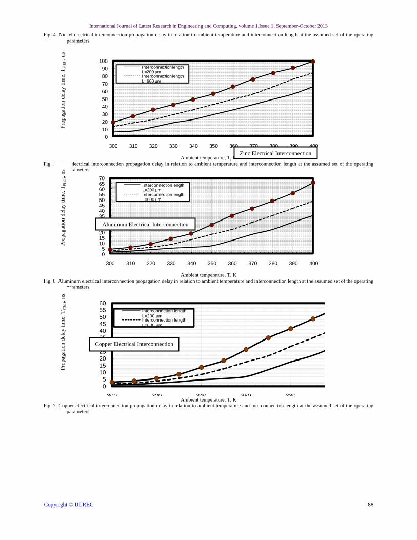
i) Figs. (4-7) have assured that signal propagation delay through electrical interconnections increases with increasing both interconnection length and ambient temperature for different types of electrical interconnections under study.
ii) Also as shown in Figs. (4-7) have indicated that copper electrical interconnection has presented the lowest signal propagation delay compared to other electrical interconnection under the same operating conditions.
iii) As shown in Figs. (8-11) have assured that data transmission bit rate through electrical interconnections decreases with increasing both interconnection length and ambient temperature for different types of electrical interconnections under study.
iv) As well as shown in Figs. (8-11) have indicated that copper electrical interconnection has presented the highest data transmission bit rate compared to other electrical interconnections under the same operating conditions.
v) As shown in Figs. (12-14) have assured that signal propagation delay through optical interconnections increases with increasing both interconnection length and ambient temperature for different types of optical interconnections under study.
10
22
34
46
58
70
82
94
106
118130
300 310 320 330 340 350 360 370 380 390 400
Interconnection length L=200 ìmInterconnection length L=600 ìm
Ambient temperature, T, K
Pro
paga
tion
del
ay ti
me,
TP(
EI), n
s
Nickel Electrical Interconnection
International Journal of Latest Research in Engineering and Computing, volume 1,Issue 1, September-October 2013
Copyright © IJLREC 88
Fig. 4. Nickel electrical interconnection propagation delay in relation to ambient temperature and interconnection length at the assumed set of the operating parameters.
0
10
20
30
4050
60
70
80
90
100
300 310 320 330 340 350 360 370 380 390 400
Interconnection length L=200 ìmInterconnection length L=600 ìm
Ambient temperature, T, K
Fig. 5. Zinc electrical interconnection propagation delay in relation to ambient temperature and interconnection length at the assumed set of the operating parameters.
05
10152025303540455055606570
300 310 320 330 340 350 360 370 380 390 400
Interconnection length L=200 ìmInterconnection length L=600 ìm
Ambient temperature, T, K
Fig. 6. Aluminum electrical interconnection propagation delay in relation to ambient temperature and interconnection length at the assumed set of the operating parameters.
05
1015202530354045505560
300 320 340 360 380
Interconnection length L=200 ìmInterconnection length L=600 ìm
Ambient temperature, T, K
Fig. 7. Copper electrical interconnection propagation delay in relation to ambient temperature and interconnection length at the assumed set of the operating parameters.
Pro
paga
tion
dela
y tim
e, T
P(E
I), n
s
Zinc Electrical Interconnection
Pro
paga
tion
del
ay ti
me,
TP(
EI), n
s
Aluminum Electrical Interconnection
Pro
paga
tion
del
ay ti
me,
TP
(EI), n
s
Copper Electrical Interconnection

International Journal of Latest Research in Engineering and Computing, volume 1,Issue 1, September-October 2013
Copyright © IJLREC 89
05
1015202530354045505560
200 300 400 500 600 700 800 900 1000
Room temperature T0= 300 KAmbient temperatutre T= 350 K
Interconnection length, L, ìm
Fig. 8. Nickel electrical interconnection data transmission bit rate in relation to ambient temperature and interconnection length at the assumed set of the operating parameters.
0102030405060708090
100110120130
200 300 400 500 600 700 800 900
Room temperature T0= 300 KAmbient temperatutre T= 350 K
Interconnection length, L, ìm
Fig. 9. Zinc electrical interconnection data transmission bit rate in relation to ambient temperature and interconnection length at the assumed set of the operating parameters.
050
100150200250300350400450500
200 300 400 500 600 700 800 900
Room temperature T0= 300 KAmbient temperatutre T= 350 K
Interconnection length, L, ìm
Fig. 10. Aluminum electrical interconnection data transmission bit rate in relation to ambient temperature and interconnection length at the assumed set of the operating parameters.
Dat
a tr
ansm
issi
on b
it ra
te, B
R(E
I), M
bit/
s
Nickel Electrical Interconnection
Dat
a tr
ansm
issi
on b
it r
ate,
BR
(EI), M
bit/s
Zinc Electrical Interconnection
Aluminum Electrical Interconnection
Dat
a tr
ansm
issi
on b
it ra
te, B
R(E
I), M
bit/s

International Journal of Latest Research in Engineering and Computing, volume 1,Issue 1, September-October 2013
Copyright © IJLREC 90
0
100
200
300
400
500
600
700
200 300 400 500 600 700 800 900
Room temperature T0= 300 KAmbient temperatutre T= 350 K
Interconnection length, L, ìm
Fig. 11. Copper electrical interconnection data transmission bit rate in relation to ambient temperature and interconnection length at the assumed set of the operating parameters.
0
0.05
0.1
0.15
0.2
0.25
0.3
0.35
0.4
0.45
0.5
300 310 320 330 340 350 360 370 380 390 400
Interconnection length L=200 ìmInterconnection length L=600 ìm
Ambient temperature, T, K
Fig. 12. Silica optical interconnection propagation delay in relation to ambient temperature and interconnection length at the assumed set of the operating parameters.
00.05
0.10.15
0.20.25
0.30.35
0.40.45
0.50.55
0.6
300 310 320 330 340 350 360 370 380 390 400
Interconnection length L=200 ìmInterconnection length L=600 ìm
Ambient temperature, T, K
Fig. 13. Polymethyl metha acrylate optical interconnection propagation delay in relation to ambient temperature and interconnection length at the assumed set of the operating parameters.
Dat
a tr
ansm
issi
on b
it ra
te, B
R(E
I), M
bit/
s P
ropa
gatio
n de
lay
time,
TP(
OI), n
s
Silica optical Interconnection
Copper Electrical Interconnection
Pro
paga
tion
dela
y tim
e, T
P(O
I), n
s
PMMA optical Interconnection

International Journal of Latest Research in Engineering and Computing, volume 1,Issue 1, September-October 2013
Copyright © IJLREC 91
00.05
0.10.15
0.20.25
0.30.35
0.40.45
0.50.55
0.60.65
0.7
300 320 340 360 380
Interconnection length L=200 ìmInterconnection length L=600 ìm
Ambient temperature, T, K
Fig. 14. Polystyrene optical interconnection propagation delay in relation to ambient temperature and interconnection length at the assumed set of the operating parameters.
02.5
57.510
12.515
17.520
22.525
27.530
200 300 400 500 600 700 800 900
Room temperature T0= 300 KAmbient temperatutre T= 350 K
Interconnection length, L, ìm
Fig. 15. Silica optical interconnection data transmission bit rate in relation to ambient temperature and interconnection length at the assumed set of the operating parameters.
0
2
4
6
8
10
12
14
16
200 300 400 500 600 700 800 900 1000
Room temperature T0= 300 KAmbient temperatutre T= 350 K
Interconnection length, L, ìm
Fig. 16. Polymethyl metha acrylate optical interconnection data transmission bit rate in relation to ambient temperature and interconnection length at the assumed set of the operating parameters.
Pro
paga
tion
del
ay ti
me,
TP
(OI), n
s
PS optical Interconnection
Dat
a tr
ansm
issi
on b
it ra
te, B
R(O
I), G
bit/s
Silica optical Interconnection
D
ata
tran
smis
sion
bit
rate
, BR
(OI), G
bit/s
PMMA optical Interconnection

International Journal of Latest Research in Engineering and Computing, volume 1,Issue 1, September-October 2013
Copyright © IJLREC 92
0123456789
1011
200 300 400 500 600 700 800 900 1000
Room temperature T0= 300 KAmbient temperatutre T= 350 K
Interconnection length, L, ìm
Fig. 17. Polystyrene optical interconnection data transmission bit rate in relation to ambient temperature and interconnection length at the assumed set of the operating parameters.
0.01
0.1
1
10
300 310 320 330 340 350 360 370 380 390 400
Nickel EI
Zinc EI
Aluminum EI
Ambient temperature, T, K
Fig. 18. Electrical and optical interconnection propagation delay in relation to ambient temperature and interconnection length at the assumed set of the operating parameters.
0.1
1
10
100
1000
300 320 340 360 380
Nickel EI
Zinc EI
Aluminum EI
Ambient temperature, T, K
Fig. 19. Electrical and optical interconnection propagation delay in relation to ambient temperature and interconnection length at the assumed set of the operating parameters.
0
0.1
0.2
0.3
0.4
0.5
0.6
0.7
200 300 400 500 600 700 800 900 1000
Nickel EI
Zinc EI
D
ata
tran
smis
sion
bit
rate
, BR
(OI), G
bit/s
PS optical Interconnection
Pro
paga
tion
dela
y tim
e, T
P(O
I) ,T
P(E
I), n
s P
ropa
gati
on d
elay
tim
e, T
P(O
I) ,T
P(E
I), n
s D
ata
tran
smis
sion
bit
rate
, BR
(EI), G
bit/
s
Electrical interconnection operation at room temperature (T0=300 K)
Interconnection length (L=200 ìm)
Interconnection length (L=1000 ìm)

International Journal of Latest Research in Engineering and Computing, volume 1,Issue 1, September-October 2013
Copyright © IJLREC 93
Interconnection length, L, ìm Fig. 20. Variations of data transmission bit rate for electrical interconnection against interconnection length at the assumed set of the operating parameters.
0
0.025
0.05
0.075
0.1
0.125
0.15
0.175
0.2
0.225
0.25
200 300 400 500 600 700 800 900 1000
Nickel EI
Zinc EI
Interconnection length, L, ìm
Fig. 21. Variations of data transmission bit rate for electrical interconnection against interconnection length at the assumed set of the operating parameters.
2.55
7.510
12.515
17.520
22.525
27.530
200 300 400 500 600 700 800 900 1000
Silica OI
Interconnection length, L, ìm
Fig. 22. Variations of data transmission bit rate for optical interconnection against interconnection length at the assumed set of the operating parameters.
1
1.5
2
2.5
3
3.5
4
4.5
5
5.5
200 300 400 500 600 700 800 900 1000
Silica OI
Interconnection length, L, ìm
Fig. 23. Variations of data transmission bit rate for optical interconnection against interconnection length at the assumed set of the operating parameters.
Dat
a tr
ansm
issi
on b
it ra
te, B
R(E
I), G
bit/
s Electrical interconnection operation at high temperature (T=400 K)
Dat
a tr
ansm
issi
on b
it ra
te, B
R(O
I), G
bit/s
Optical interconnection operation at room temperature (T0=300 K)
Optical interconnection operation at high temperature (T=400 K)
Dat
a tr
ansm
issi
on b
it r
ate,
BR
(OI), G
bit/s

International Journal of Latest Research in Engineering and Computing, volume 1,Issue 1, September-October 2013
Copyright © IJLREC 94
vi) Also as shown in Figs. (12-14) have indicated that silica optical interconnection has presented the lowest signal propagation delay compared to other optical interconnection under the same operating conditions.
vii) As shown in Figs. (15-17) have assured that data transmission bit rate through optical interconnections decreases with increasing both interconnection length and ambient temperature for different types of optical interconnections under study.
viii) Also as shown in Figs. (15-17) have indicated that silica optical interconnection has presented the highest data transmission bit rate compared to other optical interconnections under the same operating conditions.
ix) Figs. (18-23) have demonstrated that the bad effects of increasing temperature and interconnection dimensions on both electrical and optical interconnections. Optical interconnections have presented lower signal propagation delay and higher data transmission bit rate compared to electrical interconnection under the same operating considerations.
CONCLUSIONS Integrated optics are considered as a possible alternative to overcome metallic interconnect limitations that can be the barrier for further gigascale integration predicted by optical interconnection. These expectations are focused on the latency and data transmission bit rates mainly, which should be lower when the optical interconnects are applied. It is theoretically found that the increased interconnection length and surrounding ambient temperatures have dramatically effect on the data transmission bit rates for both electrical and optical interconnections.
REFERENCES 1. K. Yashiki, N. Suzuki, K. Fukatsu, T. Anan, H. Hatakeyama, andM. Tsuji, �1.1 ìm Range High Speed Tunnel Junction vertical cavity surface emitting
lasers,� IEEE Photon. Technol. Lett., vol. 19, no. 23, pp. 1883�1885, Dec. 2007.
2. Ahmed Nabih Zaki Rashed, �New Trends of Forward Fiber Raman Amplification for Dense Wavelength Division Multiplexing (DWDM) Photonic Communication Networks,� International Journal of Soft Computing, Vol. 6, No. 2, pp. 26-32, 2011.
3. N. C. Helman, J. E. Roth, D. P. Bour, H. Altug, and D. A. B. Miller, �Misalignment-tolerant surface-normal low-voltage modulator for optical interconnects,� IEEE J. Sel. Topics Quantum Electron., vol. 11, no. 2, pp. 338�342, Mar./Apr. 2005.
4. Q. Xu, B. Schmidt, S. Pradhan, and M. Lipson, �Micrometre-scale silicon electro-optic modulator,� Nature, vol. 435, no. 7040, pp. 325�327, May 2005.
5. Ahmed Nabih Zaki Rashed, �Transmission Performance Evaluation of Optical Add Drop Multiplexers (OADMs) in Optical Telecommunication Ring Networks,� American Journal of Engineering and Technology Research, Vol. 11, No. 10, pp. 12-21, Oct. 2011.
6. D. A. van Blerkom, C. Fan, M. Blume, and S. C. Esener, �Transimpedance receiver design optimization for smart pixel arrays,� J. Lightw. Technol., vol. 16, no. 1, pp. 119�126, Jan. 1998.
7. Ahmed Nabih Zaki Rashed, �High Transmission Bit Rate of Multi Giga Bit per second for Short Range Optical Wireless Access Communication Networks� International Journal of Advanced Science and Technology, Vol. 32, pp. 23-32, July 2011.
8. P. Kapur, R. D. Kekatpure, and K. C. Saraswat, �Minimizing power dissipation in optical interconnects at low voltage using optimal modulator design,� IEEE Trans. Electron. Devices, vol. 52, no. 8, pp. 1713�1721, Aug. 2005.
9. H. Cho, P. Kapur, and K. C. Saraswat, �A modulator design methodology minimizing power dissipation in a quantum well modulator-based optical interconnect,� J. Lightw. Technol., vol. 25, no. 6, pp. 1621�1628, Jun. 2007.
10. O. Kibar, D. A. van Blerkom, C. Fan, and S. C. Esener, �Power minimization and technology comparison for digital free space optoelectronics
interconnects,� J. Lightw. Technol., vol. 17, no. 4, pp. 546�555, Apr. 1999.
11. B. Analui, D. Guckenberger, D. Kucharski, and A. Narasimha, �A fully integrated 20-Gb/s optoelectronic transceiver implemented in a standard 0.13-ìm
CMOS SOI Technology,� IEEE J. Solid-State Circuits, vol. 41, no. 12, pp. 2945�2955, Dec. 2006.
12. Ahmed Nabih Zaki Rashed, �Optical Add Drop Multiplexer (OADM) Based on Dense Wavelength Division Multiplexing Technology in Next Generation Optical Networks,� American Journal of Engineering and Technology Research, Vol. 11, No. 11, pp. 48-61, Nov. 2011.
13. N. C. Helman, J. E. Roth, D. P. Bour, H. Altug, and D. A. B. Miller, �Misalignment-tolerant surface-normal low-voltage modulator for optical interconnects,� IEEE J. Sel. Topics Quantum Electron., vol. 11, no. 2, pp. 338�342, Mar./Apr. 2005.
14. Y. Leblebici and S. Kang, �Modeling and simulation of hot-carrier induced device degradation in MOS circuits,� IEEE J. Solid-State Circuits, vol. 28, no. 5, pp. 585�595, May 1993.
15. J. Montanaro et al., �A 160 MHz, 32 b, 0.5 W CMOS RISC microprocessor,� IEEE J. Solid-State Circuits, vol. 31, no. 11, pp. 1703�1714, Nov. 1996.
16. D. A. B. Miller, �Physical reasons for optical interconnection,� Int. J. Optoelectron., vol. 11, no. 3, pp. 155�168, 1997.
17. D. A. B. Miller, D. S. Chemla, T. C. Damen, A. C. Gossard, W. Wiegmann, T. H. Wood, and C. A. Burrus, �Electric field dependence of optical
absorption near the band gap of quantum-well structures,� Phys. Rev. B, Condens. Matter, vol. 32, no. 2, pp. 1043�1060, Jul. 1985.
18. A. F. Benner, M. Ignatowski, J. A. Kash, D. M. Kuchta, and M. B. Ritter, �Exploitation of optical interconnects in future server architectures,� IBM J.
Res. & Dev., Vol. 49, pp. 755-775, 2005.
19. T. Agerwala, and M. Gupta, �Systems research challenges: A scale-out perspective,� IBM J. Res. & Dev., Vol. 50, pp. 173-179, 2006.
International Journal of Latest Research in Engineering and Computing, volume 1,Issue 1, September-October 2013
Copyright © IJLREC 95
20. S. Nakagawa, D. Kuchta, C. Schow, R. John, L. A. Coldren, Y.-C. Chang, �1.5 mW/Gbps low power optical interconnect transmitter exploiting high-efficiency VCSEL and CMOS driver,� Tech. Dig. Optical Fiber Communication Conf., San Diego, CA, Feb. 2008.
21. C. Kromer, G. Sialm, C. Berger, T. Morf, M. L. Schmatz, F. Ellinger, D. Erni, G.-L. Bona, and H. Jackel, �A 100 mW 4 x 10 Gb/s transceiver in 80-nm CMOS for high density optical interconnects,� IEEE J. Solid-State Circuits, Vol. 40, pp. 2667-2679, 2005.
22. C. Schow, F. Doany, O. Liboiron-Ladouceur, C. Baks, D. Kuchta, L. Schares, R. John, and J. Kash, �160 Gb/s, 16 channel full-duplex, single-chip CMOS optical transceiver,� Tech. Dig. Optical Fiber Communication Conf., Anaheim, CA, March 2007.
23. P. Kapur and K. C. Saraswat, "Comparisons Between Electrical and Optical Interconnects for On Chip Signaling," Proceedings of the IEEE International International Interconnect Technology Conference, pp. 89-91, June 2002.
24. Y. I. Ismail and E. G. Friedman, "Sensitivity of Interconnect Delay to On-Chip Inductance," Proceedings of the IEEE International Symposium on Circuits and Systems, pp. 403-406, May 2000.
25. G. Chen and E. G. Friedman, "Low Power Repeaters Driving RC Interconnect with Delay and Bandwidth Constraints," Proceedings of the IEEE International SOC Conference, pp. 335-339, September 2004.
26. R. A. Soref and B. R. Bennett, "Electro optical Effects in Silicon," IEEE Journal of Quantum Electronics, Vol. 23, No. 1, pp. 123-129, January 1987.
27. A. Liu et al., "A High-Speed Silicon Optical Modulator Based on a Metal-Oxide-Semiconductor Capacitor," Nature, Vol. 427, pp. 615-618, February 2004.
28. O. Boyraz and B. Jalali, "Demonstration of a Silicon Raman Laser," Optical Express, Vol. 12, No. 21, pp. 5269-5273, Oct. 2004.
29. Y. A. Vlasov and S. J. McNab, "Losses in Single Mode Silicon-On-Insulator Strip Waveguides and Bends," Optical Express, Vol. 12, No. 8, pp. 1622- 1631, April 2004.
30. S. V. Averine, Y. C. Chan, and Y.L. Lam, "Geometry Optimization of Interdigitated Schottky Barrier Metal-Semiconductor-Metal Photodiode Structures," Solid-State Electronics, Vol. 45, No. 3, pp. 441-446, March 2001.
31. J. Oh et al., "Interdigitated Ge p-i-n Photodetectors Fabricated on a Si Substrate Using Graded SiGe Buffer Layers," IEEE Journal of Quantum Electronics, Vol. 38, No. 9, pp. 1238-1241, Sep. 2002.
32. J. Oh, S. K. Banerjee, and J.C. Campbell, "Metal Germanium-Metal Photodetectors on Heteroepitaxial Ge-on-Si with Amorphous Ge Schottky Barrier Enhancement Layers," IEEE Photonics Technology Letters, Vol. 15, No. 5, pp. 745-747, May 2003.
33. M. A. El-Moursy and E. G. Friedman, "Optimum Wire Sizing of RLC Interconnect with Repeaters," Proceedings of the IEEE Great Lakes Symposium on VLSI, pp. 27-32, April 2003.
AUTHOR's BIOGRAPHY Author's Profile
Dr. Ahmed Nabih Zaki Rashed was born in Menouf city, Menoufia State, Egypt country in 23 July, 1976. Received the B.Sc., M.Sc., and Ph.D. scientific degrees in the Electronics and Electrical Communications Engineering Department from Faculty of Electronic Engineering, Menoufia University in 1999, 2005, and 2010 respectively. Currently, his job carrier is a scientific lecturer in Electronics and Electrical Communications Engineering Department, Faculty of Electronic Engineering, Menoufia university, Menouf. Postal Menouf city code: 32951, EGYPT. His scientific master science thesis has focused on polymer fibers in optical access communication systems. Moreover his scientific Ph. D. thesis has focused on recent applications in linear or nonlinear passive or active in optical networks. His interesting research mainly focuses on transmission capacity, a data rate product and long transmission distances of passive and active optical communication networks, wireless communication, radio over fiber communication systems, and optical network security and management. He has published many high scientific research papers in high quality and technical international journals in the field of advanced communication systems, optoelectronic devices, and passive optical access communication networks. His areas of interest and experience in optical communication systems, advanced optical communication networks, wireless optical access networks, analog communication systems, optical filters and Sensors.
As well as he is editorial board member in high academic scientific International research Journals. Moreover he is a reviewer member in high impact scientific research international journals in the field of electronics, electrical communication systems, optoelectronics, information technology and advanced optical communication systems and networks. His personal electronic mail ID (E-mail:[email protected]). His published paper under the title "High reliability optical interconnections for short range applications in high performance optical communication systems" in Optics and Laser Technology, Elsevier Publisher has achieved most popular download articles in 2013.