Embed Size (px)
Citation preview
Departamento de Física de la Materia Condensada Instituto de Nanociencia de Aragón (INA)
Instituto de Ciencias de Materiales de Aragón (ICMA)
Universidad de Zaragoza-CSIC
TESIS DOCTORAL
Electrical conduction and magnetic
properties of nanoconstrictions and
nanowires created by focused
electron/ion beam and of
Fe3O4 thin films
Memoria presentada por D. Amalio Fernández-Pacheco Chicón a la Facultad de Ciencias de la Universidad de Zaragoza, para optar al grado de Doctor en Ciencias Físicas
Zaragoza, mayo de 2009

Resumen de la tesis doctoral
La tecnología existente en los discos duros de los ordenadores actuales,
de usotan generalizado en la sociedad actual, representa uno de los primeros
ejemplos de aplicación directa de la nanotecnología en el campo de la
electrónica, donde coexisten la producción en masa del producto con los
límites existentes del nanomagnetismo, es decir, con los procesos magnéticos
fundamentales en la escala nanométrica. El extremo control de los granos
constituyentes de la información, respecto a su estabilidad térmica y sus
campos de inversión de la imanación, han permitido un grado de
almacenamiento 107 veces mayor desde la salida al mercado, en 1957 por IBM,
del primer disco duro.
Este aumento exponencial en el rendimiento de almacenaje ha sido
llevado a cabo gracias a avances tecnológicos de gran impacto. Un ejemplo
paradigmático es el descubrimiento de la magnetorresistencia gigante (GMR)
por Albert Fert [1] y Peter Grunberg [2], por lo que recibieron el premio Nobel
en 2007. Este fenómeno relaciona la configuración magnética de ciertas
estructuras y su resistencia eléctrica con una sensibilidad inusitada hasta la
fecha, lo que abrió la puerta a la miniaturización de ciertos dispositivos. Este
descubrimiento es también el alma mater de otros tipos de estructuras basados
en un gran control del crecimiento de láminas delgadas, con espesores de
nanómetros.
Además, a lo largo de los últimos años se han desarrollado técnicas de
nanofabricación que permiten tallar materiales y fabricar dispositivos en los
que las dimensiones laterales de los mismos alcanzan tallas nanométricas. Este
enorme desarrollo en técnicas litográficas ha sido básicamente consecuencia de
la necesidad de una mayor miniaturización de los transistores en circuitos
integrados [3]. Así pues, otro tipo de dispositivos electrónicos se están ahora
postulando como candidatos a sustituir a los actuales, donde el magnetismo da
un paso más en su interacción con la electrónica, lo que se conoce como el área
de espintrónica.
En esta tesis se han estudiado las propiedades de transporte eléctrico,
tanto de láminas delgadas magnéticas, donde las anchuras al paso de corriente
fueron litografiadas a tamaño de micras, como otras estructuras de talla lateral
nanométrica, tanto magnéticas como no magnéticas, de gran interés tanto para
la comprensión de ciertos fenómenos físicos que se producen en estos
materiales como para su potencial aplicación en espintrónica, y en otros
campos de la nanotecnología.
Uno de las aproximaciones propuestas para el almacenamiento de la
información en el futuro son las denominadas MRAM (“Magnetic Random
Acces Memory”), memorias no volátiles magnéticas, donde la información
queda almacenada en una unión túnel magnética (MTJ), de rápido acceso y
escritura. Una MTJ consiste es un “emparedado” formado por dos electrodos
magnéticos separados por una barrera aislante (Al2O3, MgO,...). Al aplicar una
tensión eléctrica aparece una corriente constituida por electrones que realizan
el efecto túnel entre los electrodos a través de la barrera. Si al aplicar un campo
magnético permutamos entre las configuraciones magnéticas de los electrodos
paralela y antiparalela, obtenemos un efecto magnetorresistivo
(magnetorresistencia túnel: TMR) [4]. A partir de 1995 se ha desarrollado
extraordinariamente la tecnología necesaria para la realización de las uniones
túnel. Gracias a su minúsculo tamaño pueden integrarse como sensores
magnetorresistivos en cabezas lectoras así como realizar memorias no volátiles
de alta densidad de información y bajo consumo [5]. El valor de la
magnetorresistencia túnel depende de forma fundamental de una magnitud
clave: la polarización de espín, que es la diferencia normalizada de espines
“up” menos el “down” existentes en el nivel de Fermi, es decir, los
responsables de la conducción eléctrica. En la tesis doctoral hemos estudiado
el óxido de hierro Fe3O4, denominado magnetita, donde se ha predicho
teóricamente que existe un 100% de polarización de espín (a estos materiales
se les denomina “half metals”), lo cual daría en principio valores de TMR muy
altos. Previo a su implementación en dispositivos, es necesario un
conocimiento fundamental de sus propiedades de magnetotransporte en el
material en forma de lámina delgada. Resultados previos en la literatura se han
centrado en el estudio de la MR derivada de defectos estructurales,
denomiandos anti-phase boundaries, que cambian sustancialmente las
propiedades de transporte de la magnetita [6-8]. En nuestro caso, hemos
estudiado otros efectos como son el Efecto Hall Planar o el efecto Hall, de vital
importancia desde un punto de vista fundamental en la física del estado sólido
[9, 10].
Otros tipos de estructuras muy interesantes de los que se han reportado
en la literatura efectos de MR superiores al 100% son los presentes en
constricciones magnéticas de tamaño atómico, donde el hecho de que la
conducción de electrones sea de tipo balístico, y no difusivo, da lugar a una
fenomenología radicalmente diferente a la del mundo macroscópico.
Experimentos iniciales en contactos de Ni, realizados por electrodeposición y
mecánicamente, mostraron efectos acuñados como magnetorresistencia
balística (BMR) superiores a los existentes por magnetorresistencia gigante
[11, 12]. Valores también enormes se encontraron para la MR anisótropa
(BAMR) [13, 14], debidos a un aumento sustancial del acoplamiento espín-
órbita, junto con modificaciones sustanciales en la estructura electrónica [15,
16]. Sin embargo, una gran cantidad de voces en la comunidad científica se han
opuesto a estos resultados, asociándolos a efectos espurios, relacionados con la
magnetoestrición o reconfiguraciones atómicas dentro del contacto [17, 18].
Experimentos limpios, donde se minimicen posibles artefactos, parecen de esta
manera, cruciales para determinar si estos efectos son intrínsecos, o no.
Recientemente, otro tipo de memorias sugeridas por Stuart Parkin en
IBM son las denominadas “racetrack memories” [19], donde la información
viene dada por las diferentes paredes de dominio existentes en nanohilos
planares (normalmente de permaloy: NixFe1-x). La enorme reducción de las
dimensiones, junto con la posibilidad de construir las memorias en una
configuración tridimensional, permitiría alcanzar límites insospechados hasta
la fecha. Este campo está de gran actualidad, con avances significativos como
la creación de una lógica aritmética análoga a la existente en la actualidad,
basada en el movimiento de estas paredes [20], o el cambio de la imanación del
material sin necesidad de aplicar campos magnéticos externos, sino mediante el
momento de espín (“spin torque”) que produce una densidad de corriente
apreciable [21].
La tesis doctoral realizada podría dividirse en dos objetivos
fundamentales. El primero se centra en la fabricación de materiales de tamaño
micro- o nanométrico, mediante el uso de técnicas de litografía (óptica, y de
haces focalizados de electrones/iones). El segundo, el estudio de las
propiedades de transporte eléctrico, así como el magnetismo, de las estructuras
fabricadas. De forma fundamental, se han estudiado las propiedades
magnéticas y de transporte eléctrico en estructuras con alto interés en
aplicaciones en espintrónica y nanomagnetismo. A continuación, y de una
forma cronológica, se esbozan los objetivos concretos, las tareas realizadas, así
como la metodología llevada a cabo durante la tesis en los temas desarrollados.
Por completitud, las publicaciones derivadas de la investigación son también
incluidas.
A) LÁMINAS EPITAXIALESDE MAGNETITA
En primer lugar, con la llegada de los equipos de litografía óptica al
Instituto de Nanociencia de Aragón (INA), se desarrollaron y optimizaron,
junto con el equipo técnico del INA, los procesos necesarios para dicha
litografía, en láminas de magnetita (Fe3O4) crecidas epitaxialmente en la
dirección (001) sobre sustratos de óxido de magnesio (MgO). Como resultado
de dichos procesos, se fabricaron estructuras micrométricas de Fe3O4, con
materiales metálicos como oro o aluminio en los pads,derivados de una
segunda etapa de litografía, para minimizar la alta resistencia de contacto
existente en dicho óxido, de manera que el estudio se llevara a cabo en el
mayor rango de espesores y temperaturas posibles. En paralelo a dicho trabajo,
se instaló un equipo de medidas de magnetotransporte en el Instituto de
Ciencias de Materiales de Aragón (ICMA), constituido por un criostato de
ciclo cerrado y un electroimán, junto con una fuente de corriente y un
nanovoltímetro. Dicha instalación consistió, entre otras tareas, en el desarrollo
de todos los programas de control de los dispositivos vía PC.
Las propiedades de magnetotransporte de los electrodos de Fe3O4 fueron
ampliamente estudiados. En concreto, láminas de varios espesores (2 nm – 350
nm) mediante el método de Van der Paw, a temperatura ambiente; además
electrodos de espesores: 40, 20 y 10 nm en función de la temperatura, por
encima y por debajo de la transición de Verwey (transición metal-aislante),
típica de este material medio-metálico. El estudio sistemático fue hecho en
medidas de magnetorresistencia (MR) en diferentes configuraciones, y de
voltajes transversales al paso de la corriente, como son el efecto Hall anómalo
y el efecto Hall Planar, de alto interés fundamental y tecnológico. Al efecto
Hall ordinario no se pudo acceder con los campos utilizados en un laboratorio
convencional, con lo que el estudio se completó realizando experimentos en
una gran infraestructura europea en Nijmegen (Holanda), el laboratorio de altos
campos magnéticos (HFML) perteneciente a la Universidad de Radboud-
Nijmegen. Como consecuencia de todo este trabajo se han realizado 4
publicaciones científicas [I-IV].
B) NANOCONSTRICCIONES DE METALES MAGNÉTICOS
El siguiente paso de la tesis fue la creación de estructuras de variado
carácter, con la llegada al INA de un equipo “Dual Beam”. Dicho instrumento
consta de una columna de haces focalizados de electrones (FEB) y de iones de
Galio (FIB), con energía de aceleración máxima de 30 kV. Dichas columnas
permiten visualizar y fabricar estructuras con tamaños mínimos del orden de 10
nm. Este magnífico equipo de nanolitografía fue complementado con una
plataforma para la medida de transporte eléctrico, de manera simultánea a la
toma de imágenes o procesado de la muestra.
Así pues, en primer lugar comentaremos el trabajo realizado en la
fabricación de nanoconstricciones de tamaño atómico en materiales metálicos
magnéticos, con importantes aplicaciones en dispositivos para espintrónica. En
la tesis, se llevó a cabo el desarrollo de un proceso para la fabricación de estos
nanocontactos atómicos, con control simultáneo de la resistencia, lo que
permite tallar dichos materiales a tamaños muy por debajo de la resolución del
equipo de litografía. La estabilización de los contactos en contacto con la
atmósfera, así como el estudio de magnetorresistencia balística (BMR) y
magnetorresistencia anisótropa balística (BAMR) ha sido estudiada en una
cantidad sustancial de muestras. Como resultado, 3 publicaciones científicas se
han llevado a cabo [V-VII].
C) NANOHILOS FABRICADOS MEDIANTE HACES
FOCALIZADOS DE ELECTRONES E IONES
Una gran cantidad de la tesis ha estado relacionada con la creación de
nanoestructuras mediante el depósito de materiales con el FEB o FIB (focused-
electron/ion-beam- induced-deposition: FEBID/FIBID). Esta técnica de
nanolitografía consiste en el depósito mediante fase vapor (CVD) de metales
inducido por el haz de electrones o iones, una vez que un gas precursor ha sido
introducido en la cámara. Los haces focalizados disocian las moléculas del gas,
que ha quedado adsorbido en la superficie, creando un depósito localizado
donde el haz ha sido escaneado. La resolución nanométrica del haz se traduce
en depósitos también nanométricos. Esta técnica no está muy extendida entre la
comunidad científica, si es comparada por ejemplo con la litografía electrónica
(EBL). Sin embargo, tiene una ventaja evidente respecto a ésta, y es que se
consigue una resolución espacial similar, usando una técnica de un solo paso,
evitando el depósito intermedio de resinas poliméricas, lo que permite una
flexibilidad mucho mayor en la creación de nanoestructuras. Durante mi tesis,
he estudiado nanohilos fabricados con esta técnica usando los gases
precursores: (CH3)3Pt(CpCH3), W(CO)6 y Co2(CO)8. La gran riqueza de
procesos que acaecen en este tipo de técnica da lugar a una riquísima
fenomenología que he estudiado en gran profundidad, especialmente en el caso
del primer y tercer precursor.
En concreto, para los depósitos de Pt-C con el primer gas
[(CH3)3Pt(CpCH3)], hemos observado diferencias sustanciales en la
composición de los depósitos, dependiendo de si el proceso se llevaba a cabo
con FEB o FIB [VIII], habiendo detectado una transición metal-aislante en
función de la cantidad de Pt existente en los nanohilos [IX]. Esto puede
entenderse en el marco de la teoría de sólidos desordenados establecida por
Mott [22], donde la matriz carbonosa que acoge las inclusiones metálicas de Pt
es un semiconductor amorfo, que es dopado con dichas impurezas, y que a
consecuencia del desorden existente tiene niveles localizados dentro del gap
del semiconductor, así como un alargamiento de las bandas.
En el caso de depósitos usando el segundo precursor [W(CO)6] crecidos
por FIBID, el importante grado de desorden, así como la naturaleza amorfa del
material, da lugar a un superconductor con una temperatura crítica de unos 5 K,
temperatura sustancialmente mayor que el W metálico puro [23]. Mediante una
colaboración con el grupo del profesor Vieira en la Universidad Autónoma de
Madrid, se ha podido observar mediante espectroscopia túnel (STS) que
depósitos de dicho material es un paradigma de superconductor de tipo II que
sigue la teoría BCS [X]. Además, se ha podido estudiar la dependencia de la
red de Abrikosov de los vórtices en dicho material en función de la temperatura
y campo magnético con gran detalle mediante STS [XI], observando que la
fusión de dicha red 2D se produce a través de una fase hexática intermedia
[XII]. Mi aportación fundamental a este estudio ha sido el análisis
composicional y químico de los depósitos de W-C mediante espectroscopía
fotoelectrónica de rayos X (XPS). Posteriormente, se ha hecho un estudio
comparativo de las propiedades de transporte superconductoras de micro- y
nanohilos mediante esta técnica, llegando a la conclusión que las propiedades
superconductoras son similares para tallas laterales del orden de 100 nm, lo que
da cuenta de una buena funcionalidad superconductora de dicho material a
escala nanométrica [XIII].
Por último, con el último precursor se han crecido nanohilos de cobalto.
La alta eficacia de disociación de este precursor permite crear nanoilos
tremendamente puros (del orden del 90% atómico). Este hecho, determinado
por análisis de dispersión de electrones (EDX), ha sido corroborado mediante
medidas de magnetotransporte [XIV] y de magnetometría óptica de efecto Kerr
logitudinal (MOKE) con alta resolución espacial [XV]. Esta última técnica se
usó en el transcurso de una estancia de dos meses en el Blackett laboratory en
el Imperial College (Londres), en el grupo del profesor Russel Cowburn.
Durante esta estancia se realizó un estudio de los campos de propagación y
nucleación de paredes de dominio de estos nanohilos (XVI], para determinar si
dichas estructuras son interesantes en aplicaciones de lógica aritmética basada
en el movimiento de paredes de dominio [20], así como en memorias
magnéticas no volátiles (“racetrack memories”) [19]. Además, se estudió el
acoplamiento magnético de electrodos de diferentes formas unidos mediante
una constricción de unos 400 nm de anchura, estudio complementado con el
trabajo con otro grupo localizado en Berkeley (California), que estudió esos
mismos dispositivos mediante microscopía de transmisión de rayos X (STXM),
lo que permite resolver zonas magnéticas de la muestra (mediante dicroísmo
magnético) con una resolución espacial de unos 40 nm). Estas configuraciones
han sido estudiadas mediante simulaciones micromagnéticas, usando el código
de acceso libre OOMMF [24].
Publicaciones de la tesis doctoral
[I] J. M. De Teresa, A. Fernández-Pacheco, L. Morellón, J. Orna, J. A. Pardo, D. Serrate, P.A. Algarabel, M.R. Ibarra, Magnetotransport properties of Fe3O4 thin films for applications in Spin Electronics, Micr. Eng. 84 1660 (2007)
[II] A. Fernández-Pacheco, J. M. De Teresa, J. Orna, L. Morellón, P.A. Algarabel, J. A. Pardo, M.R. Ibarra, Universal Scaling of the Anomalous Hall Effect in Fe3O4 thin films, Phys. Rev. B (Rapid com.) 77, 100403(R) (2008)
[III] A. Fernández-Pacheco, J. M. De Teresa, J. Orna, L. Morellon, P. A. Algarabel, J. A. Pardo, M. R. Ibarra, C. Magen, E. Snoeck, Giant planar Hall effect in epitaxial Fe3O4 thin films and its temperature dependence, Phys. Rev. B 78, 212402 (2008)
[IV] A. Fernández-Pacheco, J. M. De Teresa, P.A. Algarabel, J. Orna, L. Morellón, J. A. Pardo, M.R. Ibarra, Hall Effect and magnetoresistance measurements in Fe3O4 thin films up to 30 Tesla, manuscript in preparation.
[V] A. Fernández-Pacheco, J. M. De Teresa, R. Córdoba, and M. R. Ibarra, Exploring the conduction in atomic-sized metallic constrictions created by controlled ion etching Nanotechnology 19, 415302 (2008)
[VI] J. V. Oboňa, J. M. De Teresa, R. Córdoba, A. Fernández-Pacheco, and M. R. Ibarra, Creation of stable nanoconstrictions in metallic thin films via progressive narrowing by focused-ion-beam technique and in-situ control of resistance, Microel. Eng. (2009) in press
[VII] A. Fernández-Pacheco, J. M. De Teresa, R. Córdoba, and M. R. Ibarra, Tunneling and anisotropic-tunneling magnetoresistance in iron nanoconstrictions fabricated by focused-ion-beam, submitted to MRS proceedings (2009)
[VIII] J. M. De Teresa, R.Córdoba, A. Fernández-Pacheco, O. Montero, P. Strichovanec, and M.R. Ibarra, Origin of the Difference in the Resistivity of As-Grown Focused-Ion and Focused-Electron-Beam-Induced Pt Nanodeposits, J. Nanomat. 2009, 936863 (2009)
[IX] A. Fernández-Pacheco, J. M. De Teresa, R. Córdoba, M. R. Ibarra, Conduction regimes of Pt-C nanowires grown by Focused-Ion–Beam induced deposition: Metal-insulator transition, Phys. Rev. B, 79, 174204 (2009)
[X] I. Guillamón, H. Suderow, S. Vieira, A. Fernández-Pacheco, J. Sesé, R. Córdoba, J. M. De Teresa, M. R. Ibarra, Nanoscale superconducting properties of amorphous W-based deposits grown with a focused-ion-beam , New Journal of Physics 10, 093005 (2008)
[XI] I. Guillamón, H. Suderow, S. Vieira, A. Fernández-Pacheco, J. Sesé, R. Córdoba, J. M. De Teresa, M. R. Ibarra, Direct observation of melting in a 2-D superconducting vortex lattice, manuscript in preparation
[XII] I. Guillamón, H. Suderow, S. Vieira, A. Fernández-Pacheco, J. Sesé, R. Córdoba, J. M. De Teresa, M. R. Ibarra, Superconducting density of states at the border of an amorphous thin film grown by focused-ion-beam, Journal of Physics: Conference Series (2009), in press
[XIII] J. M. De Teresa, A. Fernández-Pacheco, R. Córdoba, J. Sesé, M. R. Ibarra, I. Guillamón, H. Suderow, S. Vieira, Transport properties of superconducting amorphous W-based nanowires fabricated by focused-ion-beam-induced-deposition for applications in Nanotechnology, submitted to MRS proceedings (2009)
[XIV] A. Fernández-Pacheco, J. M. De Teresa, R. Córdoba, M. R. Ibarra, Magnetotransport properties of high-quality cobalt nanowires grown by focused-electron-beam-induced deposition, J. Phys. D: Appl. Phys. 42 055005 (2009)
[XV] A. Fernández-Pacheco, J. M. De Teresa, R. Córdoba, M. R. Ibarra D. Petit , D. E. Read, L. O'Brien, E. R. Lewis, H. T. Zeng, R. P. Cowburn, Systematic study of the magnetization reversal in Co wires grown by focused-electron-beam-induced deposition, manuscript in preparation
[XVI] A. Fernández-Pacheco, J. M. De Teresa, R. Córdoba, M. R. Ibarra D. Petit , D. E. Read, L. O'Brien, E. R. Lewis, H. T. Zeng, R. P. Cowburn, Domain wall conduit behaviour in cobalt nanowires grown by Focused-Electron-Beam Induced Deposition, Appl. Phys. Lett. 94, 192509 (2009)
REFERENCIAS
[1] M. N. Baibich et al., Phys. Rev. Lett. 61 2472 (1988)
[2] G. Binasch, et al., Phys. Rev. B 39, 4828 (1989)
[3] G. E. Moore, Int. Electronic Devices Meeting (IEDM) 75, 11(1975)
[4] M. Julliere, Phys. Lett. A 54, 225(1975)
[5] S. S. S. Parkin et al., J. Appl. Phys. 85, 5828 (1999)
[6] W. Eerenstein et al., Phys. Rev. Lett. 88, 247204 (2002)
[7] W. Eerestein et al, Phys. Rev. B 66, 201101(R) (2002)
[8] D. T. Margulies et al., Phys. Rev. Lett. 79, 5162 (1997)
[9] H. X. Tang et al, Phys. Rev. Lett 90, 107201 (2003)
[10] S. Onoda et al, Phys. Rev. Lett. 97, 126602 (2006)
[11] N. García et al, Phys. Rev. Lett. 82, 2923 (1999)
[12] J. J. Verlslujis et al, Phys. Rev. Lett. 87, 026601 (2001)
[13] A. Sokolov et al, Nat. Nanotechnology 2, 171 (2007)
[14] M. Viret et al, Eur. Phys. J. B 1, 1 (2006)
[15] W. F. Egelhoff et al, J. Appl. Phys 95, 7554 (2004)
[16] S. –F. Shi et al, Nat. Nanotech. 2, 522 (2007)
[17] J. Velev et all, Phys. Rev. Lett. 94,127203 (2005)
[18] D. Jacob et al, Phys. Rev. B 77, 165412 (2008)
[19] S. S. P. Parkin et al, Science 320 190 (2008)
[20] D. A. Alwood et al, Science 309 1688 (2005)
[21] D. C. Ralph et al, J. Magn. Magn. Mat. 320, 1190 (2008)
[22] N. F. Mott, and E. A. Davis, Electronic Processes in Non-Crystalline Materials, Oxford University Press (1971)
[23] E. S. Sadki, et al, Appl. Phys. Lett. 85 6206 (2004)
[24] El código OOMMF está disponible en la dirección web
http://math.nist.gov/oommf/

Conclusiones y perspectivas
Esta tesis doctoral se ha basado en el estudio de las propiedades de
magnéticas y de transporte eléctrico en materiales nanométricos, en un amplio rango
de escalas: láminas delgadas de Fe3O4, nanoconstricciones de tamaño atómico, y
nanohilos. En este capítulo se resumen las principales conclusiones de dicho trabajo,
así como perspectivas de futuro resultantes de éste. Primero se expondrán
conclusiones generales, relacionadas con las técnicas experimentales usadas, así como
los métodos de nueva creación desarrollados. En segundo lugar, se expondrán
conclusiones específicas de la tesis, en los temas en los que se ha trabajado: láminas
delgadas de Fe3O4, nanoconstricciones creadas por haces focalizados de iones, y
nanohilos creados mediante el depósito local de materiales, usando haces focalizados
de electrones e iones.
Conclusiones generales
Esta tesis doctoral ha sido posible gracias a la sinergia de dos institutos de
investigación de Zaragoza: el Instituto (mixto, CSIC-Universidad de Zaragoza) de
Ciencias de Materiales de Aragón (ICMA), con una larga y reputada experiencia en la
investigación de ciencias de materiales, y el Instituto (Universidad de Zaragoza) de
Nanociencia de Aragón (INA), de reciente creación. Ésta es la primera tesis defendida
en esta región donde se han usado equipos de micro y nanolitografía “top-down”
pertenecientes a instituciones de Zaragoza. Durante ésta, nuevos métodos y
procedimientos se han desarrollado, que serán usados en el futuro por integrantes de
ambos institutos. De especial relevancia son el desarrollo y optimización de algunos
de los procesos de litografía óptica y nanolitografía, la puesta en marcha de un equipo
para medidas de magnetotransporte, así como protocolos para el control eléctrico de
dispositivos, durante el proceso de nanolitografía en un equipo “Dual Beam”, pioneros
en el ámbito internacional.
Láminas epitaxiales de Fe3O4
Debido a su alta polarización de espín, Fe3O4 es de alto interés en aplicaciones
de espintrónica. Por ello, las propiedades de magnetotransporte en láminas de Fe3O4
crecidas de forma epitaxial en MgO (001) han sido estudiadas exhaustivamente. Los
procesos de fotolitografía llevados a cabo, han permitido el estudio de las
componentes longitudinal y transversal del tensor resistividad, así como su
dependencia con la imanación del material, por encima y debajo de la transición de
Verwey.
Medidas de resistividad y magnetorresistencia reproducen resultados previos
en la literatura, evidenciando el carácter epitaxial de las láminas. Las propiedades de
transporte de las láminas ultra-finas están sustancialmente dominadas por la presencia
de “antiphase-boundaries”. Este hecho es también evidente en el estudio sistemático
del Efecto Hall Planar, que tiene como consecuencia un valor récord para dicho
voltaje transversal a temperatura ambiente. Por debajo de la transición de Verwey,
hemos medido valores colosales, hasta la fecha nunca conseguidos en ningún otro
material, en el rango de los mΩcm. Los cambios observados en la magnetorresistencia
anisótropa, tanto en lo concerniente a su signo como valor absoluto, en función de a
temperatura, no están todavía bien entendidos, y deberían ser estudiados en
profundidad en ele futuro.
El estudio del efecto Hall Anómalo a lo largo de cuatro órdenes de magnitud
de la conductividad longitudinal, ha dado como consecuencia un resultado
experimental relevante. La dependencia σH ∝ σxx1.6 se cumple en todos los casos, sin
importar qué mecanismo de conducción sea responsable del transporte, el mayor o
menor grado de importancia en la dispersión de las “anti-phase boundaries”, etc. Esta
dependencia es universal para toda clase (material masivo, policristalino, láminas finas
epitaxiales…) de magnetita donde se ha medio el efecto Hall anómalo, así como para
todos los compuestos cuya conducción es bastante baja (en el régimen “sucio” de
conductividades). En nuestra opinión, se deberían desarrollar teorías que clarifiquen
cómo el modelo que explica este comportamiento, se adecua a un transporte no
metálico, como son la mayoría de materiales en este régimen.
Las primeras uniones-túnel magnéticas, basadas en electrodos de Fe3O4 con
barrera túnel de MgO están en este momento (2009) siendo crecidas en nuestro
laboratorio por J. Orna. Esperamos que la importante experiencia adquirida en esta
tesis en lo referente a las propiedades de magnetotransporte y procesos de
fotolitografía contribuya a un exitoso desarrollo de estos complejos dispositivos.
Creación de constricciones de tamaño atómico usando un haz focalizado de iones
Se ha desarrollado un nuevo método para la creación controlada de
constricciones de tamaño atómico en metales, mediante la medida simultánea de la
conducción eléctrica al mismo tiempo que se realiza un ataque usando un haz
focalizado de iones. Se ha demostrado que la técnica funciona para los materiales
metálicos cromo y hierro, fabricando constricciones atómicas estables dentro de la
cámara de preparación, en alto vacío. Este método tiene dos ventajas esenciales
respecto a otras técnicas bien establecidas en la literatura, como pueden ser el uso de
microscopios túnel, o la fractura mecánica controlada. Primero, es posible la
implantación de procesos usando un haz focalizado de iones dentro de los protocolos
estándar para la fabricación de circuitos integrados, con lo que posibles aplicaciones
basadas en nanocontactos serían incorporadas fácilmente a la industria actual.
Segundo, y concerniente a la creación de contactos atómicos en materiales
magnéticos, en los que efectos magnetorresistivos de gran cuantía se han descrito
previamente, y que han dado pie a una gran polémica debido a que no está claro si son
debidos a fenómenos intrínsecos, la adhesión de los átomos formando la constricción a
un sustrato, deberían minimizar efectos espurios, haciendo esta técnica más
conveniente que otras para este tipo de estudios.
La fragilidad de los contactos al exponerlos a condiciones ambientales ha sido
evidente en nanocontactos de hierro. Los resultados obtenidos no son sistemáticos,
aunque es claro que en algunos de los dispositivos, el carácter magnético del material
se mantiene, a pesar del ataque con iones. Los prometedores resultados de muestras en
el régimen túnel de conductividades nos hacen pensar que un estudio sistemático de la
magnetorresistencia balística y la magnetorresistencia anisótropa balística se podrá
hacer en el futuro. El desarrollo de nuevas estrategias para proteger las constricciones,
así como la posibilidad de implementar un equipo de medidas magnéticas adosado a la
cámara de fabricación, para evitar la exposición a condiciones ambientales, supondría
enormes avances para esta investigación
Nanohilos creados mediante el depósito local inducido mediante haces de
electrones e iones focalizados
Una parte importante de la tesis está dedicada al estudio de nanohilos creados
mediante estas prometedoras técnicas. El trabajo se ha realizado con tres tipos de
gases precursores: (CH3)3Pt(CpCH3), W(CO)6 and Co2(CO)8, usando, en el primera
caso, tanto haces focalizados de electrones como de iones para disociar las moléculas
del precursor, mientras que en el segundo y en el tercero se usaron iones o electrones,
respectivamente. En este tipo de depósitos locales, de forma general, el material está
compuesto de una mezcla de carbono y metal. El profundo trabajo realizado ha
permitido tener una visión general de los complejos fenómenos físicos que acaecen en
estos procesos, que producen microestructuras completamente diferentes en los
materiales depositados. En el caso del primer precursor, dicha microestructura está
compuesta de “clusters” de platino dentro de una matriz carbonosa amorfa. Con el
segundo gas, se forman depósitos con una estructura completamente amorfa de
carbono-wolframio, mientras que en tercero, es posible, mediante el uso de altas
corrientes focalizadas, el crecimiento de cobalto policristalino prácticamente puro.
Una gran cantidad de fenómenos físicos se han estudiado en cada caso, todos ellos
consecuencia de la microestructura particular del material.
En el caso de nanohilos de Pt-C, hemos observado una transición metal-
aislante en función de la concentración carbono/metal. Esto parece explicar los
resultados contradictorios que existían hasta la fecha con este material, en relación a
sus propiedades de transporte. Este trabajo pone de relevancia la importancia de los
parámetros elegidos, ya que en este caso particular, nanohilos metálicos o aislantes
pueden ser fabricados “a la carta”. El descubrimiento de que la conductancia
diferencial decrece en un rango de voltajes, en el caso de las muestras más resistivas,
demuestra la validez de las teorías desarrolladas para el transporte vía “hopping” bajo
altos campos eléctricos, en estructuras nanométricas. El método usado para controlar
la resistencia mientras el depósito se lleva a cabo, análogo al usado para la creación de
constricciones, ha demostrado ser de gran utilidad, siendo ahora usado de forma
general en nuestro laboratorio.
Mediante el estudio a baja temperatura de las propiedades eléctricas de micro
y nanohilos de wolframio depositados mediante haces focalizados de iones, se ha
demostrado que estructuras con talla lateral ligeramente menor que 100 nm mantienen
sus propiedades superconductoras. Esto, junto con el hecho de que este material posee
unas propiedades sin igual, como demuestran las medidas realizadas mediante
espectroscopía túnel, en el grupo del profesor Vieira, hacen que este material sea un
superconductor nanométrico con enorme potencialidad. Dispositivos como “Nano-
SQUIDS” o nanocontactos para medir reflexión Andreev son ejemplos de aplicaciones
muy prometedoras, que en este momento se están llevando a cabo en nuestro grupo.
El trabajo llevado a cabo con cobalto depositado mediante haces focalizados
de electrones, demuestra que es posible crecer este material con hasta un 90% de
pureza, mediante el uso de corrientes moderadamente altas. Como resultado, las
propiedades de magnetotransporte de nanohilos de cobalto depositados en esas
condiciones son similares a las de hilos del mismo material, fabricados mediante
técnicas de nanolitografía más convencionales. El efecto de usar corrientes menores ha
sido evidenciado, mediante la degradación de dichas propiedades. Mediante el uso del
efecto magneto-óptico Kerr, resuelto en espacio, hemos estudiado ciclos de histéresis
en hilos individuales, en un amplio rango de relaciones de aspecto. Los campos
coercitivos de estas estructuras presentan una relación lineal con el cociente
espesor/anchura, lo cual es una evidencia de que la energía magnetoestática es la que
domina las posibles configuraciones de la imanación en los hilos. En el caso de
relaciones de aspecto altas, la imanación, en remanencia, queda alineada en la
dirección longitudinal del nanohilo. Mediante la creación de nanohilos con forma de
L, y utilizando rutinas de campo magnéticas en dos direcciones, hemos demostrado
que este material presenta un buen comportamiento en conducción de paredes de
domino, fenómeno denominado en la comunidad científica como “domain wall
conduit”. Las ventajas únicas que esta técnica presenta para la fabricación de
estructuras tridimensionales, hace este resultado especialmente interesante. Pasos en
esta dirección están ahora empezándose a dar. Además, la realización de experimentos
en los que la imanación de estos nanohilos sea revertida mediante una alta densidad de
corriente, el denominado efecto de momento de espín (“spin-torque”), en vez de
mediante la aplicación de un campo magnético externo, son objetivos futuros de esta
línea de investigación.
Estudios posteriores, desde un punto de vista general, deberían ser dedicados
al estudio de los límites en resolución de estas técnicas de nanolitografía, así como a la
determinación de cuán afectadas son sus propiedades funcionales cuando alguna de
sus dimensiones se reduce sustancialmente. Otro punto importante es el de obtener
materiales metálicos completamente puros, con interés en el campo de la
nanoelectrónica, ya que una mayor funcionalidad es altamente deseada en una amplia
variedad de aplicaciones. Finalmente, la combinación de varios de estos materiales
para crear estructuras híbridas, tales como dispositivos magnéticos/superconductores,
en combinación con el buen control de la resistencia de éstos durante su crecimiento,
pueden implicar la posibilidad de estudiar nuevos y apasionantes fenómenos.

Acronyms
AF Antiferromagnetic AFM Atomic Force Microscope AHE Anomalous Hall effect AMR Anisotropic Magnetoresistance APB Antiphase Boundary APD Antiphase Domain BAMR Ballistic Anisotropic Magnetoresistance BMR Ballistic Magnetoresistance BSE Backscattered electrons CCR Closed Cycle Refrigerator CIP Current In-plane configuration CPP Current Perpendicular-to-plane configuration CPU Microprocessor CVD Chemical Vapor Deposition DW Domain Wall EBJ Electrical Break Junction EBL Electron Beam Lithography EDX Energy Dispersive X-Ray spectroscopy ES-VRH Efros-Shklovskii Variable Range Hopping FCC Face centered cubic structure FEB Focused Electron Beam FEBID Focused Electron Beam Induced Deposition FEG Field Emission Gun FIB Focused Ion Beam FIBID Focused Ion Beam Induced Deposition FM Ferromagnetic GIS Gas Injection System GMR Giant Magnetoresistance GPHE Giant Planar Hall effect HDD Hard Disk HR- High Resolution IT Information Technology LG Longitudinal geometry LMIS Liquid Metal Ion Source MBE Molecular Beam Epitaxy MBJ Mechanical Break Junctions MOKE Magneto Optical Kerr Effect MR Magnetoresistance MTJ Magnetic Tunnel Junction NW Nanowire OHE Ordinary Hall effect PE Primary electrons PG Perpendicular Geometry PECVD Plasma Enhanced Chemical Vapor Deposition PHE Planar Hall effect PLD Pulsed Laser Deposition PPMS Physical Properties Measurement System RAM Random Access Memory SCs Superconductor Materials SE Secondary Electrons

SEM Scanning Electron Microscope SP Superparamagnetism SQUID Superconducting Quantum Interference Device SRIM Stopping & Range of Ions in Matter STEM Scanning Transmission Electron Microscopy STM Scanning Tunneling Microscopy STS Scanning Tunneling Spectroscopy TEM Transmission Electron Microscopy TG Transversal Geometry TMR Tunneling Magnetoresistance TAMR Tunneling Anisotropic Magnetoresistance VRH Variable Range Hoping XPS X-Ray Photoelectron Spectroscopy XRD X-Ray Diffraction
Index
Acronyms
1. Introduction ……………………………………………………………………………… 1
1.1. Introduction to nanotechnology ……………………………………………………… 2
1.2. Introduction to nanoelectronics ……………………………………………………… 6
1.2.1. The information technology. Current limits …………………………………... 6
1.2.2. GMR Heads: Impact in the information storage ………………………………. 8
1.3. Promising future routes in nanoelectronics ………………………………………… 13
1.3.1. Semiconductor nanostructures ……………………………………………….. 13
1.3.2. Spintronics and magnetic nanostructures ……………………………………. 17 1.3.2.1. Magnetic Tunnel Junctions……………………………………………………… 17
1.3.2.2. Magnetic semiconductors ……………………………………………………..... 18
1.3.2.3. Spintronics in single electron devices ………………………………………....... 19
1.3.2.4. Spintronics with organic materials ……………………………………………… 20
1.3.2.5. Domain walls in nanostructures …………………………………………........... 20
1.3.2.6. Spin-transfer effect …………………………………………………………........ 21
1.3.3. Molecular and carbon electronics …………………………………................. 23
1.3.4. Interconnectors ………………………………………………………………. 24
1.3.5. Quantum computation ……………………………………………………….. 25
1.4. Nanostructures studied in this thesis ………………………………………………... 26
2. Experimental techniques ………………….……………………………………………. 29
2.1. Lithography techniques ……………………………………………………………... 30
2.1.1. Optical lithography …………………………………………………………... 30
2.1.2. Dual Beam system ………................................................................................ 38 2.1.2.1. Introduction …………………………………………………………………….. 38
2.1.2.2. Focused electron beam (FEB) ………………………………………………….. 40
2.1.2.3. Focused ion beam (FIB) ………………………………………………………... 42
2.1.2.4. Focused electron/ion beam induced deposition (FEBID/FIBID) ………………. 43
2.2. Electrical measurements ……………………………………………………………. 48
2.2.1. Magnetotransport measurements as a function of temperature ……………… 48
2.2.2. “In situ” electrical measurements ………......................................................... 50
2.3. Spectroscopic techniques …………………………………………………………… 52
2.3.1. Energy Dispersive X-Ray spectroscopy (EDX) ……………………………... 52
2.3.2. X-Ray Photoelectron Spectroscopy (XPS) ....................................................... 53
2.4. Spatially-resolved Magneto-Optical Kerr Effect (MOKE) …………………………. 55
2.5. Atomic Force Microscopy (AFM) ………………………………………………….. 58
2.6. Other techniques ……………………………………………………………………. 60
3. Magnetotransport properties of epitaxial Fe3O4 thin films ………………………….. 61
3.1. Introduction …………………………………………………………………………. 62
3.1.1. General properties of Fe3O4 ………………………………………………….. 62
3.1.2. Half metal prediction for Fe3O4 ……………………………………………… 64
3.1.3. Properties of epitaxial Fe3O4 thin films ……………………………………… 65
3.2. Experimental details ………………………………………………………………… 67
3.2.1. Growth of the films …………………………………………………………... 67
3.2.2. Types of electrical measurement: Van der Paw and Optical lithography……. 67
3.3. Structural and magnetic characterization ………………………………………...… 69
3.4. Resistivity …………………………………………………………………………… 71
3.4.1. Resistivity as a function of thickness (room temperature) …………………... 71
3.4.2. Resistivity as a function of temperature ……………………………………... 72
3.5. Magnetoresistance and anisotropic magnetoresistance …………………..………... 73
3.5.1. Geometries for MR measurements …………………………………………... 73
3.5.2. MR as a function of thickness (room temperature) ………………………….. 73
3.5.3. MR as a function of temperature …………………………………………….. 77
3.6. Planar Hall effect (PHE) ……………………………………………………………. 78
3.6.1. Introduction to the PHE ………………………….…………………………... 78
3.6.2. PHE as a function of thickness (room temperature) …………………………. 80
3.6.3. PHE as a function of temperature ……………………………………………. 84
3.7. Anomalous Hall effect (AHE) …………………………………………………….…. 87
3.7.1. Introduction to the AHE ………………………….………………………….. 87
3.7.2. AHE as a function of thickness (room temperature) ………………………… 91
3.7.3. AHE as a function of temperature …………………………………………… 92
3.7.4. AHE in Fe3O4. Universal behavior …………………………………………... 94
3.7.5. Fe3O4 inside the AHE dirty regime of conductivities ………………………... 97
3.8. Conclusions …………………………………………………………………………. 99
4. Conduction in atomic-sized magnetic metallic constrictions created by FIB ……... 101
4.1. Theoretical background for atomic-sized constrictions……………………………. 102
4.1.1. Introduction ………………………….……………………………………… 102
4.1.2. Conduction regimes for metals ……………………………………………... 102
4.1.3. Typical methods for the fabrication of atomic contacts ……………………. 104
4.2. Atomic constrictions in magnetic materials ……………………………………….. 106
4.2.1. Introduction ………………………….……………………………………… 106
4.2.2. Ballistic magnetoresistance (BMR) ………………………….……………... 106
4.2.3. Ballistic Anisotropic Magnetoresistance (BAMR) …………………………. 107
4.2.4. Objective of this work ……………………………………………………… 108
4.3. Experimental procedure. Example for a non-magnetic material: Chromium …..… 110
4.4. Iron nanocontacts ………………………………………………………………….. 119
4.4.1. Creation of Fe nanoconstrictions inside the chamber ………………………. 119
4.4.2. Measurements of one constriction in the tunneling regime of conduction …. 120 4.4.2.1. Creation of the constriction …………………………………………………… 120
4.4.2.2. Magnetoresistance measurements ……………………………………………... 122
4.5. Conclusions ………………………………………………………………………... 127
5. Pt-C nanowires created by FIBID and FEBID ……………………………………… 129
5.1. Nanowires created by FIBID …………………………………………………...…. 130
5.1.1. Previous results in Pt-C nanodeposits grown by FIBID ………….………… 130
5.1.2. Experimental details ………………………………………………………... 132 5.1.2.1. Deposition parameters …………………………………………………………. 132
5.1.2.2. “In situ” measurement of the resistance during the growth process …………... 132
5.1.2.3. Compositional analysis by EDX ………………………………………………. 134
5.1.2.4. Structural analysis via Scanning-Transmission-Electron-Microscopy ………... 134
5.1.2.5. XPS measurements …………………………………………………………….. 134
5.1.2.6. Transport measurements as a function of temperature ………………………... 135
5.1.3. Results ………………………………………………………………………. 136 5.1.3.1. Compositional (EDX) and structural (STEM) analysis of the deposits ……….. 136
5.1.3.2. XPS measurements …………………………………………………………….. 138
5.1.3.3. “In situ” measurements of the resistance as the NWs are grown ……………… 142
5.1.3.4. Temperature dependence of the electrical properties ……………….................. 145
5.1.4. Discussion of the results ……………………………………………………. 150
5.2. Comparison of nanowires created by FIBID and FEBID …………………………. 157
5.2.1. Experimental details ………………………………………………………... 157 5.2.1.1. Deposition parameters …………………………………………………………. 157
5.2.1.2. “In situ” electrical measurements ……………………………………………… 157
5.2.1.3. High Resolution Transmission Microscopy (HRTEM) ……………………….. 157
5.2.2. Results ……………………………………………………………………… 158 5.2.2.1. “In situ” measurements of the resistance as the NWs are grown ……………… 158
5.2.2.2. Temperature dependence of the electrical properties ………………………….. 162
5.2.2.3. HRTEM images ……………………………………………………………….. 164
5.3. Conclusions …………………………………………………………………...……. 166
6. Superconductor W-based nanowires created by FIBID ……………………………. 169
6.1. Introduction ………………………………………………………………………... 170
6.1.1. Nanoscale superconductors ………….……………………………………... 170
6.1.2. Previous results in FIBID-W ………………………………………………. 170
6.2. Experimental details ……………………………………………………………….. 172
6.2.1. HRTEM analysis ………….………………………………………………... 172
6.2.2. XPS measurements …………………………………………………………. 172
6.2.3. Electrical measurement in rectangular (micro- and nano-) wires …… 172
6.3. HRTEM analysis of FIBID-W ……………………………………………………. 174
6.4. XPS study of FIBID-W …………………………………………………………… 175
6.5. Superconducting electrical properties of micro- and nano-wires ……………..….. 179
6.5.1. Critical temperature of wires ………….……………………………………. 180
6.5.2. Critical field of nanowires ………………………………………………….. 183
6.5.3. Critical current of nanowires ……………………………………………….. 184
6.6. Study of FIBID-W by Scanning-Tunneling-Spectroscopy (STS) …………..………. 185
6.7. Conclusions and perspectives ………………………………………………...…… 187
7. Magnetic Cobalt nanostructures created by FEBID………………………………… 189
7.1. Previous results for local deposition of magnetic materials using focused beams ... 190
7.2. Experimental details ……………………………………………………………….. 191
7.2.1. Compositional analysis by EDX ………….………………………………… 191
7.2.2. HRTEM …………………………………………………………………….. 191
7.2.3. Electrical measurements of wires …………………………………………... 191
7.2.4. Spatially-resolved-MOKE ………………………………………………….. 192
7.3. Compositional (EDX) and microstructural (HRTEM) characterization ………...… 193
7.4. Magnetotransport measurements of FEBID-Co nanowires ……………………….. 196
7.4.1. Magnetotransport properties of cobalt NWs grown at high currents ………. 197
7.4.2. Magnetotransport properties of cobalt NWs grown at low beam currents ..... 203
7.5. Systematic MOKE study of rectangular nanowires………………………………... 205
7.5.1. Types of structures grown. Maximum resolution obtained. ………………... 205
7.5.2. AFM investigation of the nanowires topography............................................ 206
7.5.3. Magnetization hysteresis loops MOKE measurements …………………….. 210
7.6. Domain wall conduit behavior in FEBID-Co……………………………………… 215
7.6.1. Domain wall conduit: The concept. ………………………………………… 215
7.6.2. Creation of L-shaped nanowires...................................................................... 217
7.6.3. MOKE measurements and field routines …………………………………… 219
7.7. Conclusions ………………………………………………………………………... 225
8. Conclusions and outlook ……………………………………………………………… 227
8.1. General conclusions ……………………………………………………………….. 228
8.2. Fe3O4 epitaxial thin films ………………………………………………………….. 229
8.3. Creation of atomic-sized constrictions in metals using a Focused-Ion-Beam …….. 230
8.4. Nanowires created by Focused Electron/Ion Beam Induced Deposition ………..... 231
Bibliography ………………………………………………………………………………… 233
List of publications …………………………………………………………………………. 255

Chapter 1
Introduction
This chapter intends to serve as a general introduction to nanoelectronics. The
existing limits in the current information, silicon-based, technology are exposed. The
breakthrough that the discovery of Giant-Magnetoresistance supposed for the
information storage in hard-disk-drives is explained, as an example of how
nanoelectronics can overcome these limits. Some of the most promising materials and
effects for the future of nanoelectronics are briefly summarized, paying special
attention to the spintronics field. Finally, the types of nanostructures studied in this
thesis, from a geometrical point of view, are compared.
2 Chapter 1.Introduction
1.1. Introduction to nanotechnology
Richard Feynman, Nobel Prize in Physics in 1965, is considered to be the father
of Nanotechnology. On December, 29th 1959, he gave a talk at the annual meeting of
the American Physical Society, at the California Institute of Technology (Caltech),
called "There's Plenty of Room at the Bottom" [1]. On this famous lecture, he
predicted a vast number of applications would result from manipulating matter at the
atomic and molecular scale.
“I would like to describe a field, in which little has been done, but in which an enormous amount can be done in principle.[…] it would have an enormous number of technical applications. […] What I want to talk about is the problem of manipulating and controlling things on a small scale. […] Why cannot we write the entire 24 volumes of the Encyclopedia Britannica on the head of a pin?...”
Nanotechnology and Nanoscience could be defined as the study and control of
matter in structures between 1 and 100 nm (1 nm=10-9 m, about ten times the size of
an atom). It is a multidisciplinary field, involving areas such as physics, chemistry,
materials science, engineering or medicine. It is expected that Nanotechnology will
have an enormous impact on our economy and society during the following decades;
some perspectives even assure that the ramifications of this emerging technology
portend an entirely new industrial revolution [2]. Science and technology research in
nanotechnology promises breakthroughs in such areas as materials and manufacturing,
nanoelectronics, medicine and healthcare, energy, biotechnology, information
technology, and national security.
The reduction in size of materials supposes that any of their dimensions becomes
comparable to fundamental lengths governing the physics of the system. Therefore,
classical laws are not suitable anymore to explain many phenomena, being necessary
the use of quantum physics.
Nanomaterials can be classified as a function of the number of dimensions which
are nanometric, with the rest being macroscopic: three (nanoparticles or nanospheres),
two (nanowires or nanotubes), or one (thin films).The fabrication and characterization
1.1. Introduction to nanotechnology 3
of nanometric structures requires the use of specific sophisticated instruments, with
two main strategies for its fabrication. The top-down approximation is based on the
use of micro and nanolithography techniques to define nano-objects, starting from
bigger structures. This approach is currently used to fabricate integrated circuits.
Bottom-up, however, consists on the fabrication of complex structures by assembling
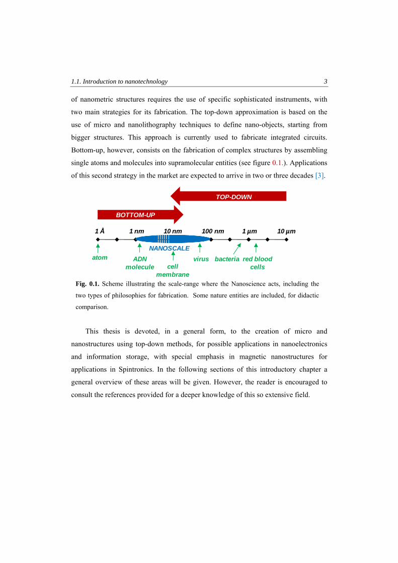
single atoms and molecules into supramolecular entities (see figure 0.1.). Applications
of this second strategy in the market are expected to arrive in two or three decades [3].
This thesis is devoted, in a general form, to the creation of micro and
nanostructures using top-down methods, for possible applications in nanoelectronics
and information storage, with special emphasis in magnetic nanostructures for
applications in Spintronics. In the following sections of this introductory chapter a
general overview of these areas will be given. However, the reader is encouraged to
consult the references provided for a deeper knowledge of this so extensive field.
Fig. 0.1. Scheme illustrating the scale-range where the Nanoscience acts, including the
two types of philosophies for fabrication. Some nature entities are included, for didactic
comparison.
1 nm 10 nm 100 nm 1 µm1 Å
NANOSCALE
BOTTOM-UP
TOP-DOWN
atom ADNmolecule
virus
10 µm
red bloodcellscell
membrane
bacteria
4 Chapter 1.Introduction
In chapter 1 we will give a general overview of nanoelectronics. The existing
limits in current technology, evidenced by the archetypical example of Moore’s law,
will be introduced. The first example of a nanotechnology-based device integrated in
industry, as it is the Giant-Magnetoresistance read heads, will be explained. We will
also summarize some of the main routes in future nanoelectronic research, to finish
with a geometrical comparison of the different nanostructures studied in the thesis:
thin films, nanowires and atomic-sized nanoconstrictions.
In chapter 2, the main experimental techniques used during the thesis will be
summarized. For fabrication: micro- (photolithography processes) and
nanolithography (Dual Beam system). And for characterization: magneto-electrical
(during and after fabrication of the structures) spectroscopic (XPS and EDX),
microscopy (SEM and AFM) and magnetometry (spatially-resolved MOKE)
techniques.
Chapter 3 is devoted to the wide study performed of the magnetotransport
properties of Fe3O4 epitaxial thin films, grown on MgO (001), which is ferrimagnetic
material with possible applications in Spintronics. The study comprises a systematic
study, as a function of temperature and film thickness, of resistivity, MR in several
geometries, AMR, PHE and AHE.
The method developed for the fabrication of atomic-sized constrictions, by the
control of the resistance of the device while a FIB etching process is done, is shown in
chapter 4. The study is centered in two metals: chromium and iron. The success in the
method in both cases, the promising MR results in the magnetic material, as well as
the problems associated with the fragility of the constrictions, are presented.
Pt-C nanowires grown by both FEBID and FIBID are studied in chapter 5. By the
in-situ and ex-situ measurement of the electrical properties of the wires, together with
a spectroscopic and microstructural characterization, a full picture for this material is
obtained, where the metal-carbon composition ratio can be used to tune their electrical
conduction properties.
1.1. Introduction to nanotechnology 5
In chapter 6, we present the results for W-based deposits grown by FIBID. The
electrical superconductor properties of this outstanding material are studied
systematically for micro and nanowires. The study is completed with spectroscopy and
high resolution microscopy measurements.
The compositional, magnetotransport, and magnetic measurements done in cobalt
nanowires grown by FEBID is shown in chapter 7. The influence of the beam current
in the purity of the structures, the dependence in the reversal of the magnetization with
shape, as well as the possibility to control domain walls in wires will be presented.
Finally, chapter 8 shows the main conclusions and perspectives of this thesis.
Last pages are dedicated to the bibliography of the different chapters, as well as
to the articles published as a consequence of this work. A list of acronyms can be
found at the beginning of the book.
6 Chapter 1. Introduction
1.2. Introduction to nanoelectronics
1.2.1. The information technology. Current limits.
The tremendous impact of information technology (IT) has become possible
because of the progressive downscaling of integrated circuits and storage devices. IT
is a key driver of today’s information society which is rapidly penetrating into all
corners of our daily life. The IT revolution is based on an “exponential” rate of
technological progress. The paradigmatic example is computer’s integration, where
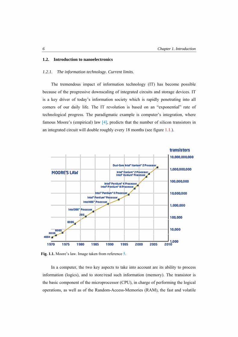
famous Moore’s (empirical) law [4], predicts that the number of silicon transistors in
an integrated circuit will double roughly every 18 months (see figure 1.1.).
In a computer, the two key aspects to take into account are its ability to process
information (logics), and to store/read such information (memory). The transistor is
the basic component of the microprocessor (CPU), in charge of performing the logical
operations, as well as of the Random-Access-Memories (RAM), the fast and volatile
Fig. 1.1. Moore’s law. Image taken from reference 5.
1.2. Introduction to nanoelectronics 7
(information is lost when power is off) type of memory in a computer. A CPU chip is
an extremely complex integrated circuit made of silicon which includes a huge
number of transistors and connecting circuitry. Nowadays, a CPU chip with an area of
1 cm2 encloses about 109 transistors [6]. This high density is obtained by the use of
projection optical lithography processes, which are able to overcome the diffraction
limit of light far away [7, 8]. In fact, the transistors are currently fabricated using the
so called 45 nm-technology [9]. This spectacular downscaling is however, reaching its
technological limits, and even before these physical limits are reached, there are strong
indications that severe engineering problems, as well as the need for huge investment,
may slow down the growth in integrated circuit performance [10]. As the limits for the
current technology are approaching, the continuation of the IT revolution must be
supported by new ideas for information storage or processing, leading to future
applications. New technologies should result in a higher integration, together with an
operation speed of hundreds of GHz, or THz. Three different routes or strategies are
today established to improve current electronics:
i. The More Moore approach: The same electronic components than currently
used are decreased in size. It is also based in designing more efficient
electronic components and better system architectures
ii. The More than Moore approach: It uses of the new functionalities appearing,
as a consequence of the gradual integration of CMOS technology.
iii. The Beyond Moore approach: It is based on the design of new system
architectures, whose building blocks may be atomic and molecular devices.
Besides, the boolean logic is substituted by more efficient algorithms, possibly
based on quantum computation.
Moore’s law is an example of a general trend for IT areas. Thus, internet traffic
doubles every 6 months, wireless capacity doubles every 9, optical capacity doubles
every 12, magnetic information storage doubles every 15, etc [11].
8 Chapter 1. Introduction
1.2.2. GMR Heads. Impact in the information storage.
To illustrate how nanoelectronics can overcome the limits of current technology,
we will show in this introduction one of the first examples where fundamental physics
concepts in the nanoscale has been a technological breakthrough, incorporated in the
mass production market, with applications widespread: the discovery of the Giant
Magnetoresistance (GMR) effect, implying the implementation of new read heads for
magnetic hard-disk drives (HDDs).
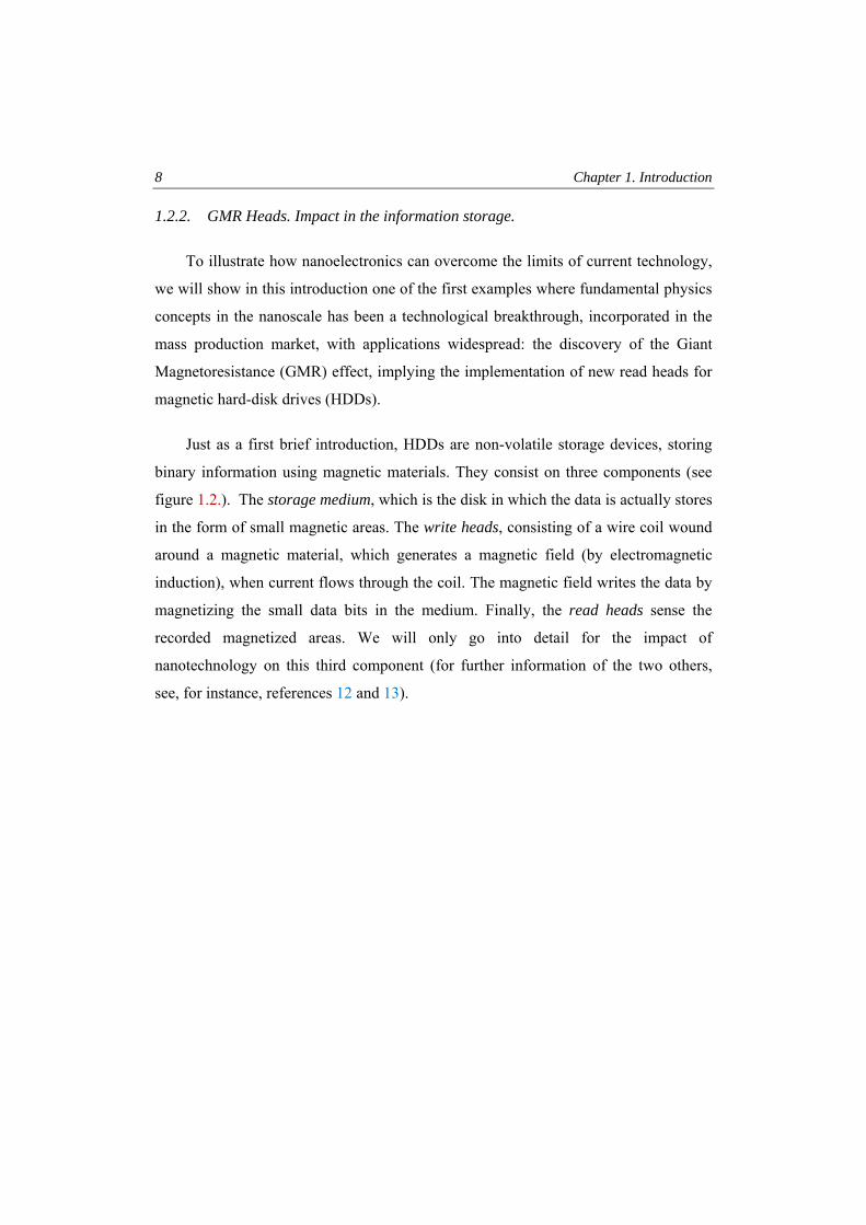
Just as a first brief introduction, HDDs are non-volatile storage devices, storing
binary information using magnetic materials. They consist on three components (see
figure 1.2.). The storage medium, which is the disk in which the data is actually stores
in the form of small magnetic areas. The write heads, consisting of a wire coil wound
around a magnetic material, which generates a magnetic field (by electromagnetic
induction), when current flows through the coil. The magnetic field writes the data by
magnetizing the small data bits in the medium. Finally, the read heads sense the
recorded magnetized areas. We will only go into detail for the impact of
nanotechnology on this third component (for further information of the two others,
see, for instance, references 12 and 13).
1.2. Introduction to nanoelectronics 9
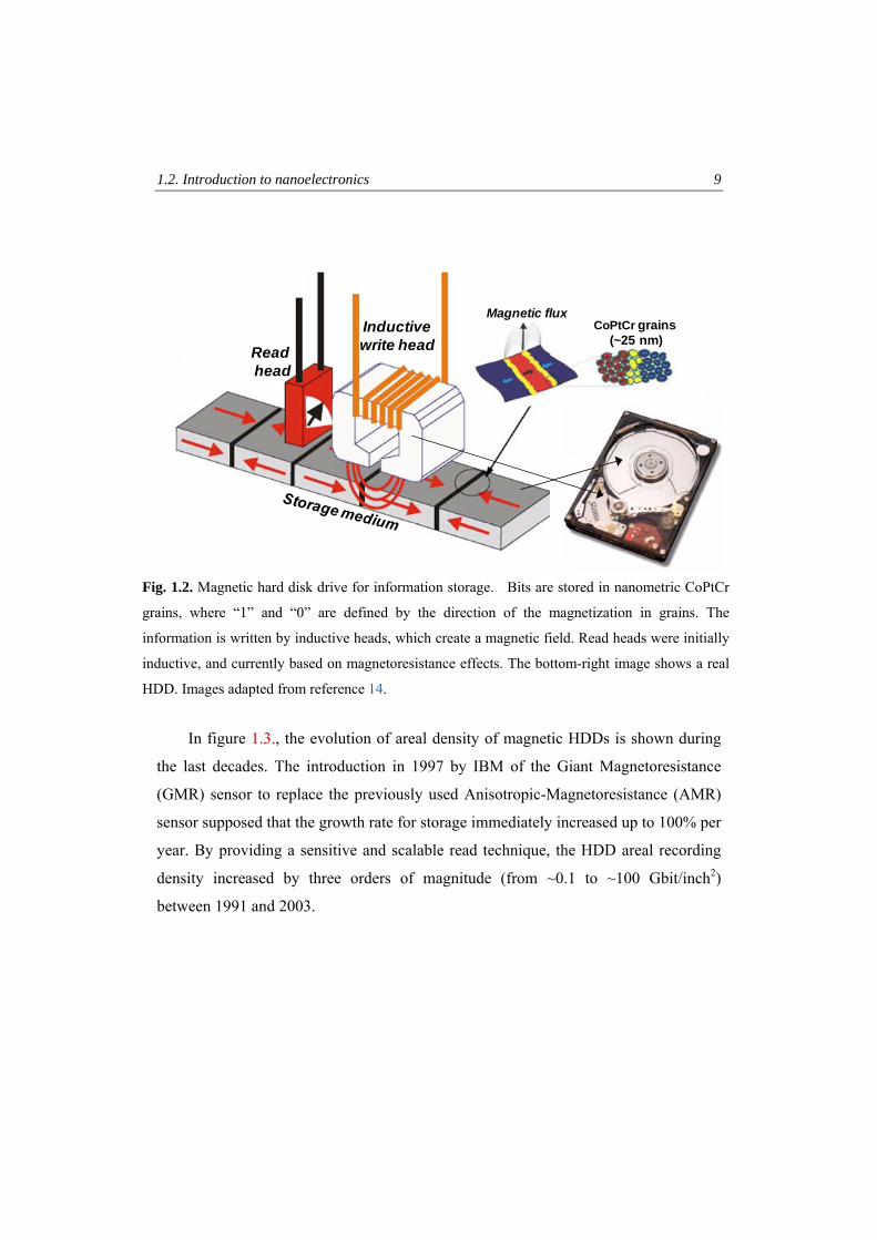
In figure 1.3., the evolution of areal density of magnetic HDDs is shown during
the last decades. The introduction in 1997 by IBM of the Giant Magnetoresistance
(GMR) sensor to replace the previously used Anisotropic-Magnetoresistance (AMR)
sensor supposed that the growth rate for storage immediately increased up to 100% per
year. By providing a sensitive and scalable read technique, the HDD areal recording
density increased by three orders of magnitude (from ~0.1 to ~100 Gbit/inch2)
between 1991 and 2003.
Magnetic fluxInductivewrite headRead
head
CoPtCr grains(~25 nm)
Fig. 1.2. Magnetic hard disk drive for information storage. Bits are stored in nanometric CoPtCr
grains, where “1” and “0” are defined by the direction of the magnetization in grains. The
information is written by inductive heads, which create a magnetic field. Read heads were initially
inductive, and currently based on magnetoresistance effects. The bottom-right image shows a real
HDD. Images adapted from reference 14.
10 Chapter 1. Introduction
We will briefly discuss the physical origin of GMR. Its discovery should be
contextualized in a time (end of 1980s) where most of the research of magnetic
nanostructures was dedicated to studies in which only one dimension of the material
was reduced to the nanoscale via thin-film deposition. The excellent control of these
processes gave rise to extensive research in the field of metallic superlattices and
heterostructures. A fascinating outcome of this research was the observation of
interlayer coupling between ferromagnetic (FM) layers separated by a non-magnetic
metallic (M) spacer [15]. This coupling oscillates from FM to antiferromagnetic (AF)
with increasing the spacer layer thickness, as RKKY interaction [16] describes. When
the FM layers thickness become comparable to the mean free path of electrons, spin-
dependent transport effects appear. In figure 1.4(a), the simplest model of the GMR
effect is schematically shown, where electrons are conducted through alternating FM
and M materials.
Fig. 1.3. Evolution of the HDD areal density in the last decades. In 1991, the introduction of
AMR-based reads supposed a growth in the areal density up to 60% per year. In 1997, the
substitution of AMR-based read heads by GMR heads supposed an immediate growth rate
increase, from 60% up to 100% per year. Future next strategies are perpendicular storage and
Tunneling magnetoresistance read heads. Image taken from reference 14.
1.2. Introduction to nanoelectronics 11
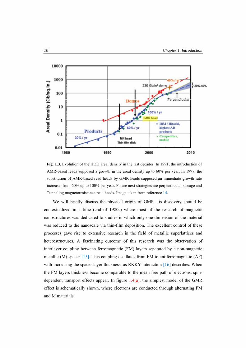
The two-current model proposed by Mott [17] and applied in ferromagnetic
metals by Fert and Campbell [18] establishes that spin-up and spin-down electrons are
conducted in two separated channels, as a consequence of the different spin-dependent
scattering probabilities. Electrons passing though the first FM get spin polarized. If the
next M layer is thin enough, this polarization is maintained, and interacts with the
second FM. This interaction results in a different resistance, depending on the relative
orientation of the FM layers (see figure 1.4(a)). For applications, devices called spin-
valves are constructed (see figure 1.4(b)), where these effects are up to 20 % at 10-20
Oe [19]. The simple concept behind spin valves consist on fixing one FM layer along
Fig. 1.4. (a) Scheme of the GMR effect. Spin-up and down electrons are conducted in two
separated channels. As a consequence, the parallel configuration is less resistive than the
antiparallel one (see text for details). (b) Scheme of the simplest spin-valve device, formed
by a fixed-FM( (top), a M, and a free-FM (bottom). (c) Two geometries for the GMR. The
CPP gives higher MR effects than CIP.
FM M M M
RP
FM FM
FM M M MFM FM
FIXED
FREE
CIP
CPP
ρ↑ = m↑ / (n↑ e2 τ↑)ρ↓ = m↓ / (n↓ e2 τ↓)
APP
2
P
PAP
ρ4ρ)ρ(ρ
ρρρGMR(%) ↑↓ −=
−= 100100
↓↑
↓↑
+=
ρρρρ
ρP
4ρρ
ρAP↓↑ +=
↓↑≠ρρ
(b)(a)
(c)
12 Chapter 1. Introduction
one orientation (normally by the AF interaction with adjacent layers), and leaving the
other free. This free layer “opens” or closes” the flow of electrons. Two types of
geometries are possible, the current-in-plane geometry (CIP), used today in sensors,
and the current-out-of-plane (CPP) (see figure 1.4(c)). The underlying GMR physical
effects are more complex than this simple explanation, being necessary the
introduction of intrinsic potentials, models in the ballistic regime of conduction, spin-
accumulation concept, etc. For details see, for instance, references 19-24.
The GMR was discovered almost simultaneously by Albert Fert’s [25] and Peter
Grünberg’s [26] groups, and, due to the huge influence in the IT, with applications in
magnetic storage, sensors and electronics [22], supposed the 2007 Nobel Prize in
Physics for both scientists. GMR is the founding effect for Spintronics. In
conventional electronic devices, the charge is the property of the electron which is
exploited. In magnetic recording, the spin (through its macroscopic manifestation, the
magnetization) is used. In Spintronics, effects where both charge and spin, and its
interplay, are studied, which are manifested in nanoscale magnetic materials.
Spintronics effects is one of the main research lines nowadays in nanoelectronics.
1.4. Promising future routes in nanoelectronics 13
1.3. Promising future routes in nanoelectronics
We will now show some effects and devices that recently have, and will have in
the future, importance in nanoelectronics. For it, five main areas will be cited [27]:
semiconductor nanostructures, Spintronics, molecular and carbon electronics,
interconnectors, and quantum computation. The aim of this section is to show some
typical quantum effects appearing in nanomaterials (discretization of energy levels,
conduction by tunneling, resonance effects, change of the energy dominating magnetic
configurations, interplay between current and spin, quantum logic…), as well as try to
give a wide idea of the most important routes that research in electronics is devoted
nowadays. The nanostructures studied during the thesis are inside one of the points of
this classification, but the physics behind them are explained in detail not here, but in
the introductory part of the corresponding chapter. The section for Spintronics is
significantly more extensive than the others, since most of the nanostructures studied
in this thesis are classified within this field.
1.3.1. Semiconductor nanostructures
As explained previously, the silicon transistors are smaller and faster every time.
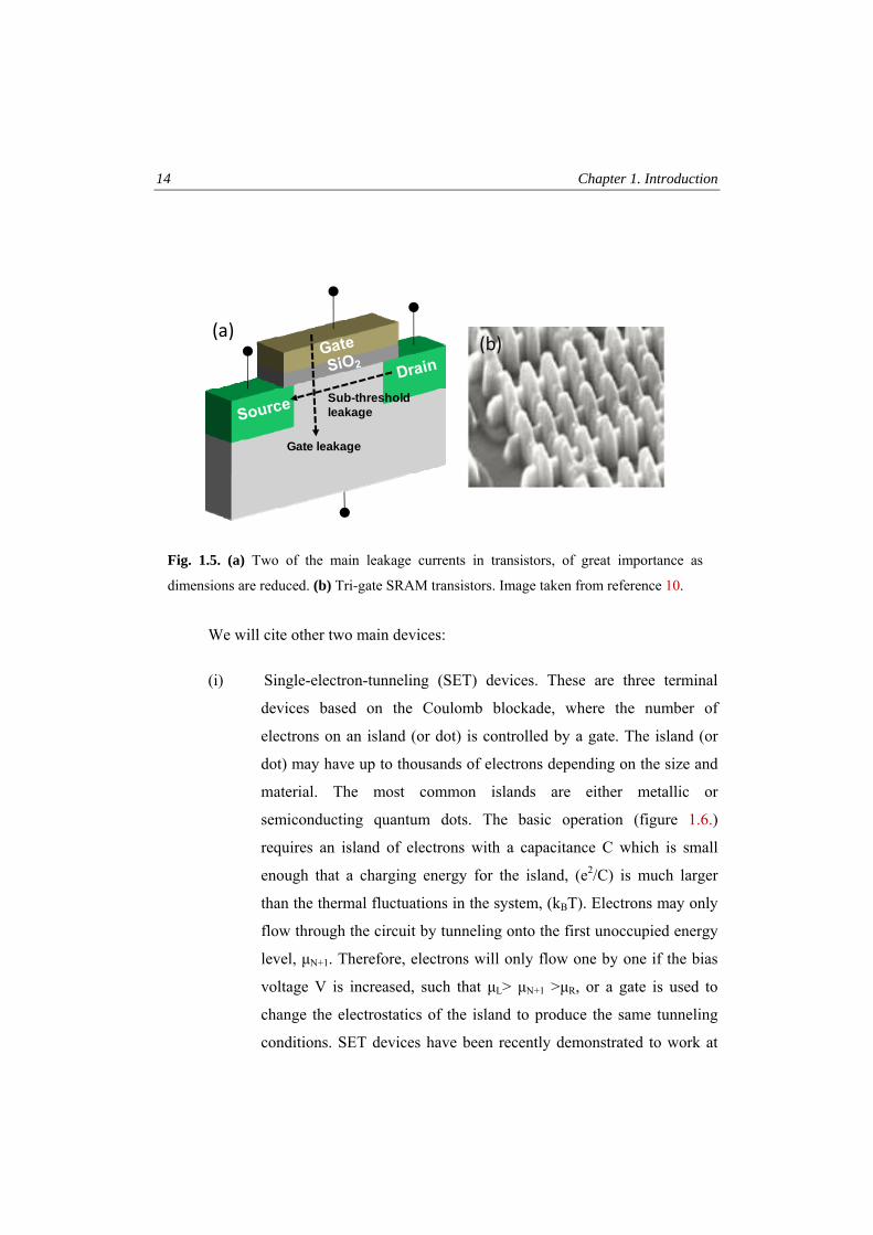
One of the main problems with the miniaturization in silicon CMOS devices is the
increasing leakage currents, between transistor source and drain, or gate-oxide leakage
(see figure 1.5(a)), which could eventually suppose a 50% of power consumption in
future [28]. Strained silicon in source and drain (instead of silicon), which increases
carrier mobility, or high-K/metal gate dielectrics (instead of traditional SiO2
dielectric), have been demonstrated to be excellent solutions to this problem, and will
continue playing a significant role over next years [10]. A transition from the currently
established planar structure to a non-planar structure [10] (the so-called tri-gate
transistor, see figure 1.5(b)) seems to be a good solution to improve performance. This
three-dimensional approach is also followed for those who use Si or other
semiconductor nanowires for the fabrication of transistors [9].
14 Chapter 1. Introduction
We will cite other two main devices:
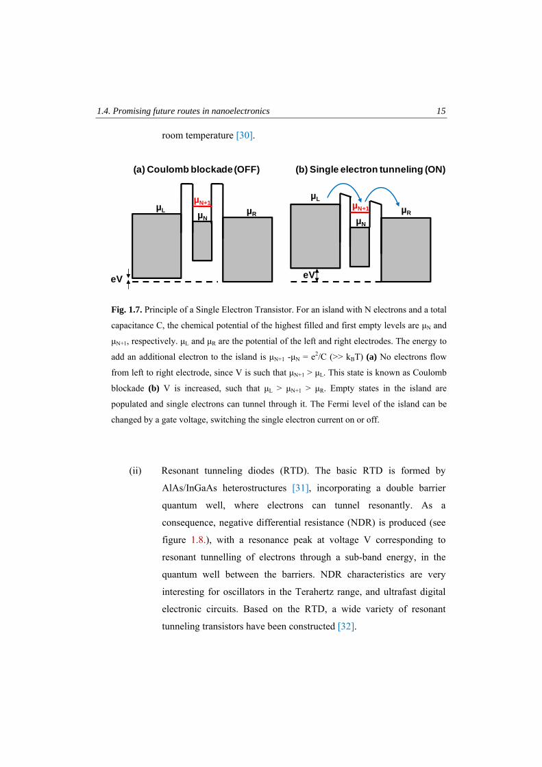
(i) Single-electron-tunneling (SET) devices. These are three terminal
devices based on the Coulomb blockade, where the number of
electrons on an island (or dot) is controlled by a gate. The island (or
dot) may have up to thousands of electrons depending on the size and
material. The most common islands are either metallic or
semiconducting quantum dots. The basic operation (figure 1.6.)
requires an island of electrons with a capacitance C which is small
enough that a charging energy for the island, (e2/C) is much larger
than the thermal fluctuations in the system, (kBT). Electrons may only
flow through the circuit by tunneling onto the first unoccupied energy
level, μN+1. Therefore, electrons will only flow one by one if the bias
voltage V is increased, such that μL> μN+1 >μR, or a gate is used to
change the electrostatics of the island to produce the same tunneling
conditions. SET devices have been recently demonstrated to work at
Sub-thresholdleakage
Gate leakage
(b)(a)
Fig. 1.5. (a) Two of the main leakage currents in transistors, of great importance as
dimensions are reduced. (b) Tri-gate SRAM transistors. Image taken from reference 10.
1.4. Promising future routes in nanoelectronics 15
room temperature [30].
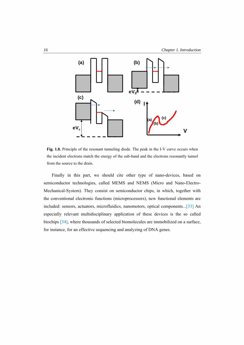
(ii) Resonant tunneling diodes (RTD). The basic RTD is formed by
AlAs/InGaAs heterostructures [31], incorporating a double barrier
quantum well, where electrons can tunnel resonantly. As a
consequence, negative differential resistance (NDR) is produced (see
figure 1.8.), with a resonance peak at voltage V corresponding to
resonant tunnelling of electrons through a sub-band energy, in the
quantum well between the barriers. NDR characteristics are very
interesting for oscillators in the Terahertz range, and ultrafast digital
electronic circuits. Based on the RTD, a wide variety of resonant
tunneling transistors have been constructed [32].
Fig. 1.7. Principle of a Single Electron Transistor. For an island with N electrons and a total
capacitance C, the chemical potential of the highest filled and first empty levels are μN and
μN+1, respectively. μL and μR are the potential of the left and right electrodes. The energy to
add an additional electron to the island is μN+1 -μN = e2/C (>> kBT) (a) No electrons flow
from left to right electrode, since V is such that μN+1 > μL. This state is known as Coulomb
blockade (b) V is increased, such that μL > μN+1 > μR. Empty states in the island are
populated and single electrons can tunnel through it. The Fermi level of the island can be
changed by a gate voltage, switching the single electron current on or off.
eV eV
µL µNµR
µN+1
µN
µN+1
(a) Coulomb blockade (OFF) (b) Single electron tunneling (ON)
µL
µRµN
16 Chapter 1. Introduction
Finally in this part, we should cite other type of nano-devices, based on
semiconductor technologies, called MEMS and NEMS (Micro and Nano-Electro-
Mechanical-System). They consist on semiconductor chips, in which, together with
the conventional electronic functions (microprocessors), new functional elements are
included: sensors, actuators, microfluidics, nanomotors, optical components...[33] An
especially relevant multidisciplinary application of these devices is the so called
biochips [34], where thousands of selected biomolecules are immobilized on a surface,
for instance, for an effective sequencing and analyzing of DNA genes.
(a) (b)
eVb(c)
eVc
(a) (b)
(c)
(d)
Fig. 1.8. Principle of the resonant tunneling diode. The peak in the I-V curve occurs when
the incident electrons match the energy of the sub-band and the electrons resonantly tunnel
from the source to the drain.
1.4. Promising future routes in nanoelectronics 17
1.3.2. Spintronics and magnetic nanostructures
A commented previously, Spintronics devices use the interplay between charge
and spin in electrons. We briefly summarize some interesting effects in nanometric
magnetic materials, different from GMR.
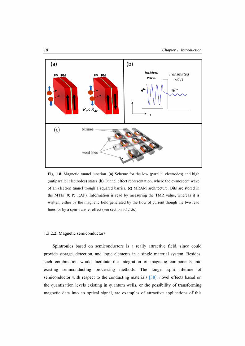
1.3.2.1. Magnetic tunnel junctions
These devices (MTJ) are similar to those exhibiting GMR (CPP configuration),
but instead of metallic barriers separating FM layers, a very thin non-magnetic
insulator, I (typically 1-3 nm) is used as barrier (see figure 1.8(a)). Electrons pass from
one FM to the other by tunnel effect, which conserves the spin. A high or low
resistance state defines a magnetoresistance (tunneling magnetoresistance, TMR) as
we previously explained in the case of GMR. More details of TMR are given in
section 3.1.2. Since the observation of a very high tunnel magnetoresistance at room
temperature by Moodera et al [35] in 1995, a great deal of research has been devoted
to this new form of spin-dependent transport. TMR values much higher than GMR can
obtained, with record values at low temperature of hundreds per cent, using MgO
barriers and half-metal electrodes [36]. From the point of view of applications, MTJs
with TMR~ 50% are used. The higher sensitivity of TMR versus GMR makes it, in
principle, more suitable for nanoelectronics. TMR read heads are, indeed, commercial
since 2005 [37], substituting the spin valve heads in HDDs. These high values have
resulted in a use for MTJs, not only for sensing, but also as another type of non-
volatile memory, to substitute HDDs: The Magnetic-Random-Access-Memory
(MRAM), see figure 1.8(c). However, the future of MTJs-based technology is now
uncertain, since MTJs have intrinsic high resistances, making impossible to maintain
current high signal-to-noise ratios with further downscaling. CPP spin valves-
memories are nowadays proposed as an alternative [19].
18 Chapter 1. Introduction
1.3.2.2. Magnetic semiconductors
Spintronics based on semiconductors is a really attractive field, since could
provide storage, detection, and logic elements in a single material system. Besides,
such combination would facilitate the integration of magnetic components into
existing semiconducting processing methods. The longer spin lifetime of
semiconductor with respect to the conducting materials [38], novel effects based on
the quantization levels existing in quantum wells, or the possibility of transforming
magnetic data into an optical signal, are examples of attractive applications of this
Fig. 1.8. Magnetic tunnel junction. (a) Scheme for the low (parallel electrodes) and high
(antiparallel electrodes) states (b) Tunnel effect representation, where the evanescent wave
of an electron tunnel trough a squared barrier. (c) MRAM architecture. Bits are stored in
the MTJs (0: P; 1:AP). Information is read by measuring the TMR value, whereas it is
written, either by the magnetic field generated by the flow of current though the two read
lines, or by a spin-transfer effect (see section 3.1.1.6.).
RP< RAP
Incident wave
eikz Teikz
z
E
Transmitted wave
FM I FM FM I FM
(b)(a)
(c)
1.4. Promising future routes in nanoelectronics 19
type of materials. The main concern in this area is the difficulty of injecting a spin into
a metal/semiconductor interface [39, 40]. The spin injection in diluted magnetic
semiconductors, such as (GaxMn1-x) has shown promising results [41], and this line of
research could be exploited in the future. The spin-FET (spin field effect transistor) by
Datta and Das [42], is one of maybe the most famous device proposed, where a
semiconductor channel between spin-polarized source and drain would transform the
spin information in large and tunable (by gate voltage) electrical signal.
1.3.2.3. Spintronics in single electron devices
The paradigmatic example is the spin-SET [43, 44], analogous to the SET
explained in section 1.3.1., but now all electrodes are magnetic, including the central
one (typically a particle). The interplay between the Coulomb effect and the
magnetism produces a coherent co-tunneling between electrodes, resulting in an
important enhancement of the TMR values.
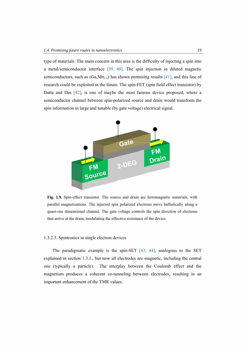
Fig. 1.9. Spin-effect transistor. The source and drain are ferromagnetic materials, with
parallel magnetizations. The injected spin polarized electrons move ballistically along a
quasi-one dimensional channel. The gate voltage controls the spin direction of electrons
that arrive at the drain, modulating the effective resistance of the device.
20 Chapter 1. Introduction
1.3.2.4. Spintronics with organic materials: molecules, carbon nanotubes and graphene
The use of organic molecules for Spintronics is really attractive. These materials
have a weak spin–orbit and hyperfine interactions, which leads to the possibility of
preserving spin-coherence over times and distances much longer than in conventional
metals or semiconductors [45]. Spectacular MR results have been obtained using the
organic molecule Alq3 in structures type FM/Alq3/FM [46] or FM/ Alq3/I/FM [47, 48],
although more systematic studies are necessary to clear out some aspects of these
devices.
MR effects of ~60% at low temperature have also been reported for carbon
nanotubes (CNTs) connecting highly spin-polarized LSCMO electrodes [49],
implying a high efficiency in spin injection in CNTs. As in the case of molecules, the
small spin-orbit coupling of carbon, together with the high Fermi velocity that limits
the carrier dwell time, are the differential aspects for a so long spin lifetime (preserved
along ~1-2 µm). Similar results are expected in spintronic devices based on graphene
(the nanometric version of graphite, formed of a few monolayers of sp2 carbon), where
spin polarization has also been demonstrated to survive over submicron distances [50].
1.3.2.5. Domain walls in nanostructures
Domain walls in nanostructures exhibit complex spin arrangements that strongly
deviate from the wall types commonly encountered in magnetic thin-film systems, and
they can be modified by changing the geometry of the element [51]. Lateral
confinement leads to pronounced geometrical effects. Various types of domain walls
arise in micro- and nanostructures because of the demagnetizing energy at the edges
[52]. This in turn offers the possibility to finely tune the wall properties, such as the
wall width. This is an important aspect, because it enables the use of domain walls as
individual tailored objects [53], and determines, for instance, the resistance or the
dynamic properties of the domain wall. Aspects such as the velocity of displacement
of domain walls, or the movement of these domains by applying external spin-
polarized currents (see next section) are now attracting much attention. The control of
1.4. Promising future routes in nanoelectronics 21
domain walls in nanowires, for memory [54] and logic devices [55] is especially
attractive, being treated in more detail in section 7.6.1. Vortex domains in circular and
squared nanostructures are also attracting much interest [56, 57], by their possible
application in information storage. The advance in a number of methods for direct,
real-space imaging in magnetic microscopy is remarkable [58], and techniques such as
the magnetic microscopy using X-ray dichroism in synchrotron sources permits, not
only sub-100nm spatial resolution, but also sub-ns time resolution observing the
magnetism dynamics in nanostructures [56, 57].
1.3.2.6. Spin-transfer effects
The normal way to change the magnetization of a ferromagnet is to apply an
external magnetic field. However, in the 1970s, theoretical [59] and experimental [60]
results indicated that a new way was possible, by the direct transfer of spin angular
momentum from a spin polarized current. Much effort has been done in the last years
regarding this effect, since the possibility to manipulate magnetization with current
would suppose a breakthrough in spin storage. The physical effect underneath is called
spin-transfer-torque, which consists on an effective torque on the magnetization of a
material, by the absorption and transfer of the transverse component of the spin
current. Spin-torque effect can be modeled by the modification of the Landau-Lifshitz-
Gilbert equation, describing the damped precession of the magnetization, in the
presence of a spin-torque effect, which compensates the damping [59, 61]:
( )HmmmmHmmeff ××+×+×−= J
dtd
dtd
00 γαγ (1.1.)
where γ0 is the gyromagnetic ratio, and α the damping coefficient. In figure 1.10. the
three terms are represented.
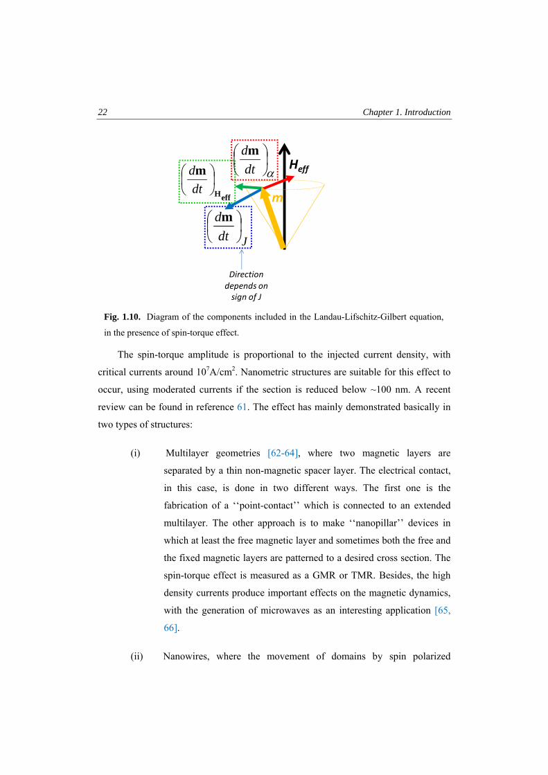
22 Chapter 1. Introduction
The spin-torque amplitude is proportional to the injected current density, with
critical currents around 107A/cm2. Nanometric structures are suitable for this effect to
occur, using moderated currents if the section is reduced below ~100 nm. A recent
review can be found in reference 61. The effect has mainly demonstrated basically in
two types of structures:
(i) Multilayer geometries [62-64], where two magnetic layers are
separated by a thin non-magnetic spacer layer. The electrical contact,
in this case, is done in two different ways. The first one is the
fabrication of a ‘‘point-contact’’ which is connected to an extended
multilayer. The other approach is to make ‘‘nanopillar’’ devices in
which at least the free magnetic layer and sometimes both the free and
the fixed magnetic layers are patterned to a desired cross section. The
spin-torque effect is measured as a GMR or TMR. Besides, the high
density currents produce important effects on the magnetic dynamics,
with the generation of microwaves as an interesting application [65,
66].
(ii) Nanowires, where the movement of domains by spin polarized
Heff
effH
m⎟⎠⎞
⎜⎝⎛
dtd α
⎟⎠⎞
⎜⎝⎛
dtdm
Jdtd
⎟⎠⎞
⎜⎝⎛ m
m
Direction depends on sign of J
Fig. 1.10. Diagram of the components included in the Landau-Lifschitz-Gilbert equation,
in the presence of spin-torque effect.
1.4. Promising future routes in nanoelectronics 23
currents has been demonstrated [54, 67]. This possibility is really
attractive, combined with applications cited in section 1.3.2.5.
1.3.3. Molecular and carbon electronics
The field of molecular electronics has had intense activity since the beginning of
1990s. Molecules have a series of advantages with respect to inorganic silicon [6]:
- Their synthesis is easily, and with low cost in many cases
- They can be grown in three dimensions as opposed to the typical 2D
semiconductor lithographic layout
- They can self-assemble
- Heat and noise production are expected to be reduced
- They can display a whole new world of properties and functionalities
- Very promising in Spintronic devices (see previous section)
Important developments have been done during the last years in molecular
electronics. We will cite [6] signal rectification, current-light converters, switches and
logic gates, realization of transistors based on molecules, heat transport and
themopower, or the study of transport in single molecules by insertion in nanogaps.
Special attention requires carbon nanotubes (CNTs) [68], perhaps the most
famous of all the nanostructures. CNT are formed by sp2 layers rolled to form a tube.
They possess unique mechanical and thermal properties. But furthermore, their
electrical properties are amazing. Electrical transport is ballistic, enabling them to
carry high currents with essentially no heating, they can exhibit metallic or
semiconducting behavior depending on their structure and dimensions… [69]. CNTs
are one of the most promising materials for the future in nanoelectronics. Devices such
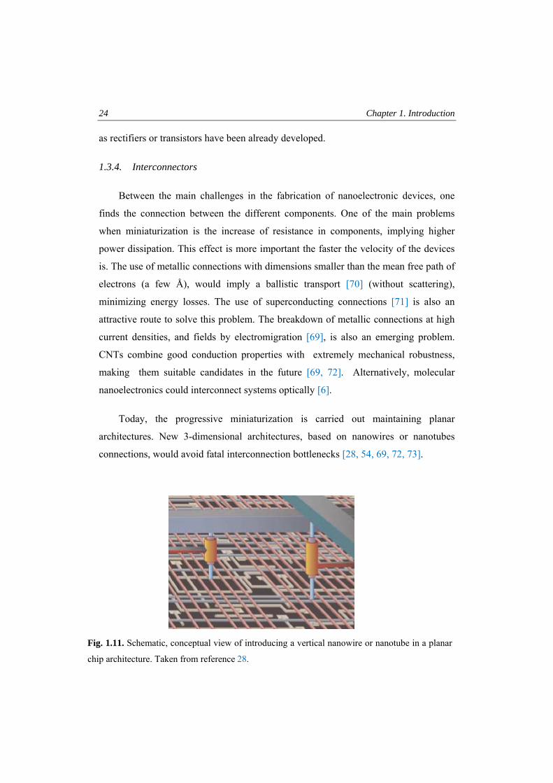
24 Chapter 1. Introduction
as rectifiers or transistors have been already developed.
1.3.4. Interconnectors
Between the main challenges in the fabrication of nanoelectronic devices, one
finds the connection between the different components. One of the main problems
when miniaturization is the increase of resistance in components, implying higher
power dissipation. This effect is more important the faster the velocity of the devices
is. The use of metallic connections with dimensions smaller than the mean free path of
electrons (a few Å), would imply a ballistic transport [70] (without scattering),
minimizing energy losses. The use of superconducting connections [71] is also an
attractive route to solve this problem. The breakdown of metallic connections at high
current densities, and fields by electromigration [69], is also an emerging problem.
CNTs combine good conduction properties with extremely mechanical robustness,
making them suitable candidates in the future [69, 72]. Alternatively, molecular
nanoelectronics could interconnect systems optically [6].
Today, the progressive miniaturization is carried out maintaining planar
architectures. New 3-dimensional architectures, based on nanowires or nanotubes
connections, would avoid fatal interconnection bottlenecks [28, 54, 69, 72, 73].
Fig. 1.11. Schematic, conceptual view of introducing a vertical nanowire or nanotube in a planar
chip architecture. Taken from reference 28.
1.4. Promising future routes in nanoelectronics 25
1.3.5. Quantum computation
The rapid miniaturization of nanoelectronics will suppose, in some point, a
crossover where quantum mechanics will govern completely the physics of the
processes, giving rise to the so called quantum computation. Quantum computers
process information in a completely different way than microprocessors, using
quantum algorithms that do not have classical analogues. From a physical point of
view a bit is a two-state system, in which one of two distinguishable states,
representing two logical values, is occupied. A qubit (quantum bit), the information
unit in quantum computers, can not only be in the state "0" or "1," it may also be in a
superposition of the two, just as a photon or an electron in a two-slit experiment can
be in a superposition of passing through one slit or the other. In a sense, a qubit carries
both values at the same time. Even more counterintuitive, two or more qubits can be
quantum entangled, which means that neither of them carries any well-defined
information on its own; rather, all information is stored in joint properties. This leads
to nonlocal correlations, with measurement on one qubit instantly defining the state of
the others, no matter how far they are apart. The use of this property supposes massive
parallel computation, solving unapproachable problems up to date, in minutes.
In principle, any two-level system can be used as a qubit. The main problem
occurs in the transmission of the quantum information, where decoherence, i.e. the
destruction of the entanglement due to non-controlled interactions with the
environment, must be avoided. For example, a tunneling process between normal
metallic junctions is incoherent, ruling these systems out as possible candidates [74].
Various systems have been demonstrated to be possible components for quantum
computers: trapped ions, neutral atoms, photons, nuclear magnetic resonance in
liquids, or superconductor components [74-79].
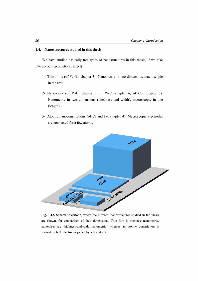
26 Chapter 1. Introduction
1.4. Nanostructures studied in this thesis
We have studied basically tree types of nanostructures in this thesis, if we take
into account geometrical effects:
1- Thin films (of Fe3O4: chapter 3): Nanometric in one dimension, macroscopic
in the rest.
2- Nanowires (of Pt-C: chapter 5, of W-C: chapter 6, of Co: chapter 7):
Nanometric in two dimensions (thickness and width), macroscopic in one
(length).
3- Atomic nanoconstrictions (of Cr and Fe, chapter 4): Macroscopic electrodes
are connected for a few atoms.
Fig. 1.12. Schematic cartoon, where the different nanostructures studied in the thesis
are shown, for comparison of their dimensions. Thin film is thickness-nanometric,
nanowires are thickness-and-width-nanometric, whereas an atomic constriction is
formed by bulk electrodes joined by a few atoms.
1.3. Nanostructures studied in this thesis 27
We can do a rough comparison of how many atoms are contained in a 10 µm× 10
µm × 10 µm cube for all these geometries considered, by assuming a typical size of
0.1 nm for an atom, and using common sizes of the materials studied. Thus, whereas a
bulk material would contain 1015 atoms, a thin film (thickness=20 nm) would have
2×10¹² atoms. In the case of a nanowire (thickness= 50nm, width=100 nm), 5 ×10¹⁰
would be contained. For nanoconstrictions, although we would calculate 1013 atoms
(and the response of them would be measured by a macroscopic probe), the electrical
conduction is dominated by a few tens of atoms, those forming the constriction and a
few neighbors in the electrodes. In this case, besides, superficial atoms are
approximately the 100%, whereas it is of the order of ~10-3% in the other geometries.
The scaling shown here when reducing dimensions is still more spectacular if
nanometric dimensions would approach the nanometer. Surface effects, defects,
confinement effects, etc get importance versus intrinsic properties as a smaller amount
of atoms plays a role in the phenomenon studied. Some of the effects studied in this
thesis are, in some way, manifestations of it.

Chapter 2
Experimental techniques
In this chapter we report on the experimental techniques used during this thesis both in
the sample patterning and characterization. An important part will be focused in the
lithography techniques and processes (micro and nano) used for the creation of
structures with a well defined geometry in these scales. The setup of an experimental
installation for the study of magnetotransport properties as a function of temperature,
as well as that for electrical measurements inside a Dual Beam chamber will be also
exposed. Spectroscopy (EDX and XPS), magnetometry (MOKE) and microscopy
(SEM and AFM) techniques used along the work are included in this chapter. Most of
the instruments described are located, in the Institute of Nanoscience of Aragón and in
the Institute of Science Materials of Aragón (ICMA). Spatially-resolved MOKE and
AFM were done in a two-month stage in the Imperial College in London, in the group
of Prof. Russell P. Cowburn.
30 Chapter 2. Experimental techniques
2.1. Lithography techniques
Lithography is the group of techniques used to transfer previously-determined
patterns on a substrate. The typical size of these structures is micro- and nano-metric.
Depending on the type of lithography technique used, the transfer is performed in a
different way, which defines the resolution that can be attained. In this thesis, we have
used two big groups of lithographies, both of them inside the top-down
approximation:
(i) Optical lithography: These techniques have been used in a clean room
environment. By far, this is the most common lithography technique in
microelectronic fabrication. It permits the fabrication of micrometric
structures
(ii) Lithography using focused electron and ion beams: This technique has been
used in a Dual Beam system. With these techniques, nanostructures below
100 nm can be patterned.
We should remark that the equipments used were installed in the Institute of
Nanoscience of Aragón (INA) premises, in Zaragoza, during the first two years of this
thesis. Thus, the protocols for a big amount of the processes that will be shown here
were carried out by myself, together with the technical staff of the Lithography
Laboratory (R. Valero, I. Rivas, and R. Córdoba), and Doctor Javier Sesé.
2.1.1. Optical lithography
All the photolithography processes have been performed in a 10,000 class-
clean room, in the INA. Clean rooms are special rooms, with well-controlled ambient
conditions. Temperature, humidity, differential pressure and flux of air, as well as
lightning and electrostatic protection have to fulfill determined standards.
Class=10,000 means that the number of particles of size=0.5 µm per cubic meter
should not be higher than 104. A deviation of these parameters can alter the processes,
as well as modify their quality.
2.1. Lithography techniques 31
We will give a short overview of the equipments and processes used, by
explaining one particular example patterned in this thesis: lithography in Fe3O4 thin
films, whose results will be presented in chapter 3.
The starting point is to create a computer layout for the specific application. We
have used the program Clewin® for it. In figure 2.1. we show the mask designed,
where the different colors symbolize different layers. Since we desire to have two
materials on top of the substrate (in this case MgO) with different shapes, it will be
necessary to perform two lithographic processes. For both patterns to be well oriented
one with respect to the other, lithography marks are added to the design (see figure
2.1(c))
Fig. 2.1. Lithography mask designed by computer. (a) Top and 3D view of the mask. The red,
blue and grey symbols symbolize a metallic material, Fe3O4 and the substrate MgO,
respectively. (b) The two patterns included in the design. Each pattern requires a separated
complete lithography process. (c) Marks used, which are necessary for the good alignment of
the two steps.
metal
Fe3O4
MgO(a)
(b) (c)
32 Chapter 2. Experimental techniques
Once the pattern is done, two photolithography masks (one for each step) are
fabricated. These masks consist on a glass plate having the desired pattern in the form
of a thin (~100 nm) chromium layer. The masks were fabricated by a company located
in the Netherlands.
As shown in figure 2.2, the lithography process involves the following steps:
(i) First step: After it, a Fe3O4 film on top of MgO has the shape shown
in figure 2.1(b)-left. The involved processes are:
(a) A thin film of Fe3O4 is epitaxially deposited on MgO (001) by
Pulsed Laser Deposition. This work is part of the thesis of Julia
Orna [1].
(b) The Fe3O4 thin film is spin coated with a photoresist. This is a
polymeric photosensitive material that can be spun onto the wafer
in liquid form. The spinning speed and photoresist viscosity will
determine the final resist thickness. For the first step, we used a
typical thickness of 2.4 µm.
(c) The substrate is soft-baked during 50 s at 100ºC in a hot plate, in
order to remove the solvents from the resist, minimizes the stress,
and improve the adhesion.
(d) The mask is aligned to the wafer, using a mask aligner by Karl
Suss®, and the photoresist is exposed to a UV source, passing
through the photomask (Hg light source, h-line: λ=405 nm),
during 50 s. The areas of the mask with chromium are completely
opaque to the light and complementary areas are transparent. The
light passes through the mask, continuing through the lenses. The
zones of photoresist which are exposed to light undergo a
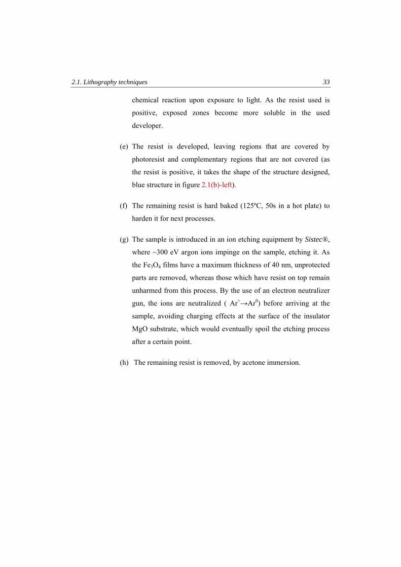
2.1. Lithography techniques 33
chemical reaction upon exposure to light. As the resist used is
positive, exposed zones become more soluble in the used
developer.
(e) The resist is developed, leaving regions that are covered by
photoresist and complementary regions that are not covered (as
the resist is positive, it takes the shape of the structure designed,
blue structure in figure 2.1(b)-left).
(f) The remaining resist is hard baked (125ºC, 50s in a hot plate) to
harden it for next processes.
(g) The sample is introduced in an ion etching equipment by Sistec®,
where ~300 eV argon ions impinge on the sample, etching it. As
the Fe3O4 films have a maximum thickness of 40 nm, unprotected
parts are removed, whereas those which have resist on top remain
unharmed from this process. By the use of an electron neutralizer
gun, the ions are neutralized ( Ar+→Ar0) before arriving at the
sample, avoiding charging effects at the surface of the insulator
MgO substrate, which would eventually spoil the etching process
after a certain point.
(h) The remaining resist is removed, by acetone immersion.
34 Chapter 2. Experimental techniques
Second step: Metallic pads are deposited on top of the Fe3O4, with the shape of
figure 2.1(b)-right. Processes
(a) The sample is spin coated with an image-reversal (negative)
photoresist. The thickness chosen was of 1.4 µm
(b) The resist is soft-baked during 50 s at 110 ºC in a hot plate.
(c) The mask is aligned to the wafer, using a mask aligner, and the
photoresist is exposed (t=10 s). In principle, the exposed zones
Fig. 2.2. Photolithography of Fe3O4 thin films. The two layers are patterned in two
separated processes. In this scheme baking steps, explained in the text, are skipped. The
photoresist profiles are exaggerated for pedagogical reasons.
(i) FIRST STEP: (Direct) patterning of Fe3O4 films
c) EXPOSURE
d) DEVELOPMENT
e) Ar ETCHING
f) REMOVAL OF RESIST
a) THIN FILM DEPOSITION (PLD)
b) PHOTORESIST DEPOSITION (+)PhotoresistFe3O4MgO
MaskU.V. Rays
Fe3O4MgO
SensibilizedPhotoresist
Ar
(ii) SECOND STEP: (Inverse) patterning of metallic pads
a) PHOTORESIST DEPOSITION (‐)
b) EXPOSURE + REVERSAL BAKE
e) METAL EVAPORATION
f) LIFT‐OFF
d) DEVELOPMENT
c) FLOOD EXPOSURE
Cross‐linkedPhotoresist
SensibilizedPhotoresist
Metal
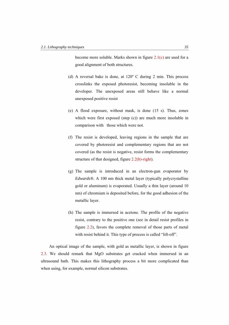
2.1. Lithography techniques 35
become more soluble. Marks shown in figure 2.1(c) are used for a
good alignment of both structures.
(d) A reversal bake is done, at 120º C during 2 min. This process
crosslinks the exposed photoresist, becoming insoluble in the
developer. The unexposed areas still behave like a normal
unexposed positive resist
(e) A flood exposure, without mask, is done (15 s). Thus, zones
which were first exposed (step (c)) are much more insoluble in
comparison with those which were not.
(f) The resist is developed, leaving regions in the sample that are
covered by photoresist and complementary regions that are not
covered (as the resist is negative, resist forms the complementary
structure of that designed, figure 2.2(b)-right).
(g) The sample is introduced in an electron-gun evaporator by
Edwards®. A 100 nm thick metal layer (typically polycrystalline
gold or aluminum) is evaporated. Usually a thin layer (around 10
nm) of chromium is deposited before, for the good adhesion of the
metallic layer.
(h) The sample is immersed in acetone. The profile of the negative
resist, contrary to the positive one (see in detail resist profiles in
figure 2.2), favors the complete removal of those parts of metal
with resist behind it. This type of process is called “lift-off”.
An optical image of the sample, with gold as metallic layer, is shown in figure
2.3. We should remark that MgO substrates get cracked when immersed in an
ultrasound bath. This makes this lithography process a bit more complicated than
when using, for example, normal silicon substrates.
36 Chapter 2. Experimental techniques
The pads are finally connected by ultrasonic wire bonding to a chip carrier,
with an instrument by Dicing Systems®. The chip carrier has macroscopic
connections, which can be manipulated in a conventional way.
The lift-off process explained has been used in other types of designs, for
applications using the Dual Beam system (see section 2.1.2). In this case, metallic
circuits are patterned by photolithography, consequently nano-lithographied by the
Dual Beam equipment. The substrate chosen for these applications is a silicon wafer,
with a 150-250 nm thick insulator on top of it (either Si3N4 deposited by Plasma-
Enhanced-Chemical-Vapor-Deposition, PECVD equipment by Sistec®, or thermally
oxidized SiO2). This layer insulates electrically the metallic pads, and, at the same
time, electrons or ions can be partially evacuated thorough the Si substrate, avoiding
charging effects, which ruin the nanolithography process.
An image of the equipments used for photolithography is shown in figure 2.4.
The minimum line width obtained routinely in our laboratory in these processes is
around 3-4 µm (better in the case of positive resist). The final resolution in an optical
process is given by the diffraction limit (λ/2, λ being the light wavelength), although
other effects such as optical aberrations of the system, the exposure mode and the
chemical process linked to the resistance are actually whom dictate the limits. In
semiconductor industry, critical dimensions below 100 nm are nowadays routinely
Au Fe3O4
MgO
Fig. 2.3. Optical image of one Fe3O4 bar with gold pads on top, which is the result of a two-
step lithography process.
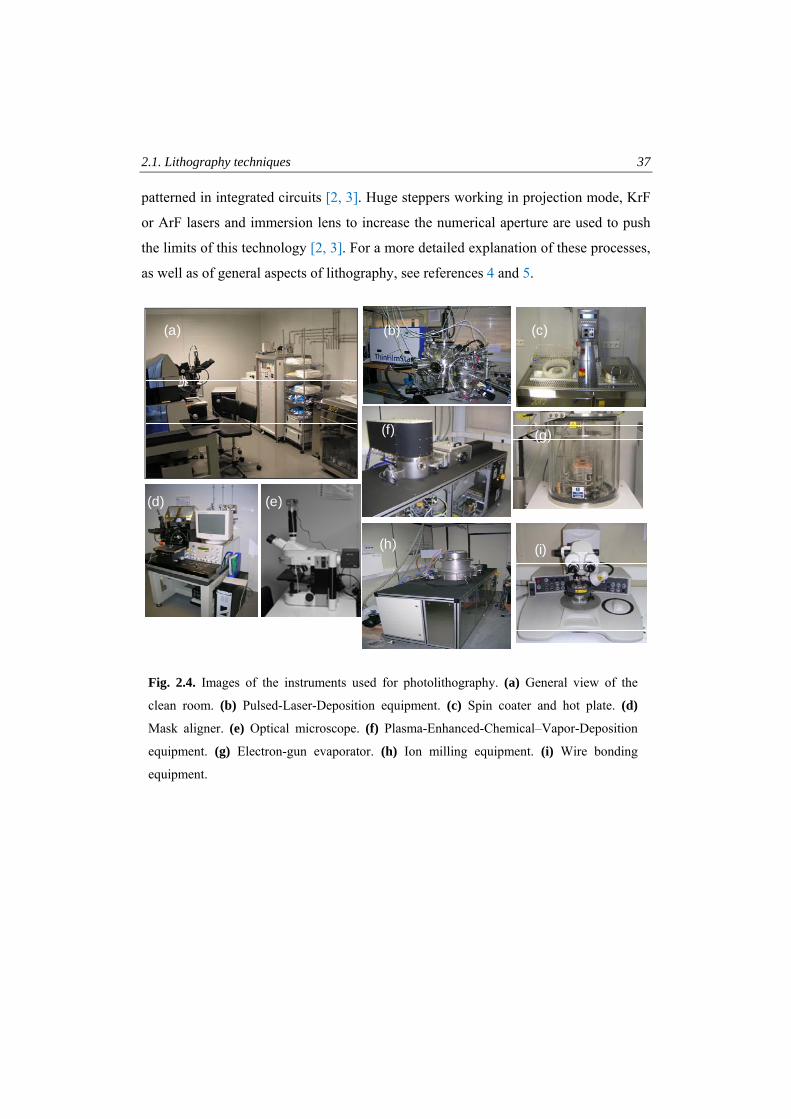
2.1. Lithography techniques 37
patterned in integrated circuits [2, 3]. Huge steppers working in projection mode, KrF
or ArF lasers and immersion lens to increase the numerical aperture are used to push
the limits of this technology [2, 3]. For a more detailed explanation of these processes,
as well as of general aspects of lithography, see references 4 and 5.
Au
(b)(a)
(d)
(c)
(e)
(f) (g)
(h) (i)
Fig. 2.4. Images of the instruments used for photolithography. (a) General view of the
clean room. (b) Pulsed-Laser-Deposition equipment. (c) Spin coater and hot plate. (d)
Mask aligner. (e) Optical microscope. (f) Plasma-Enhanced-Chemical–Vapor-Deposition
equipment. (g) Electron-gun evaporator. (h) Ion milling equipment. (i) Wire bonding
equipment.
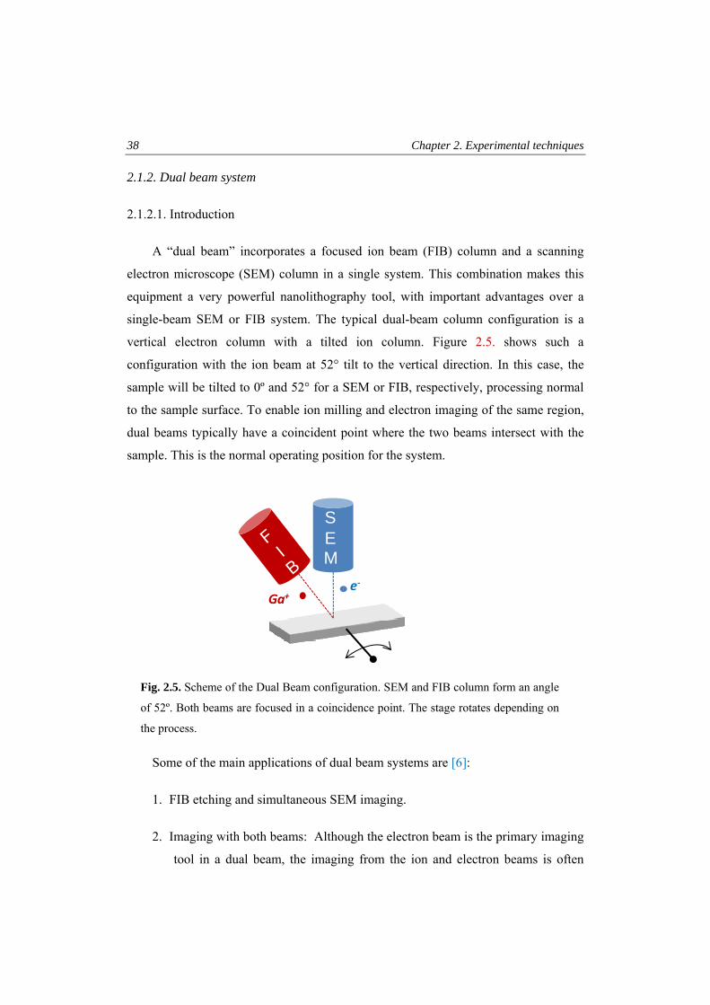
38 Chapter 2. Experimental techniques
2.1.2. Dual beam system
2.1.2.1. Introduction
A “dual beam” incorporates a focused ion beam (FIB) column and a scanning
electron microscope (SEM) column in a single system. This combination makes this
equipment a very powerful nanolithography tool, with important advantages over a
single-beam SEM or FIB system. The typical dual-beam column configuration is a
vertical electron column with a tilted ion column. Figure 2.5. shows such a
configuration with the ion beam at 52° tilt to the vertical direction. In this case, the
sample will be tilted to 0º and 52° for a SEM or FIB, respectively, processing normal
to the sample surface. To enable ion milling and electron imaging of the same region,
dual beams typically have a coincident point where the two beams intersect with the
sample. This is the normal operating position for the system.
Some of the main applications of dual beam systems are [6]:
1. FIB etching and simultaneous SEM imaging.
2. Imaging with both beams: Although the electron beam is the primary imaging
tool in a dual beam, the imaging from the ion and electron beams is often
Fig. 2.5. Scheme of the Dual Beam configuration. SEM and FIB column form an angle
of 52º. Both beams are focused in a coincidence point. The stage rotates depending on
the process.
SEM
Ga+e‐
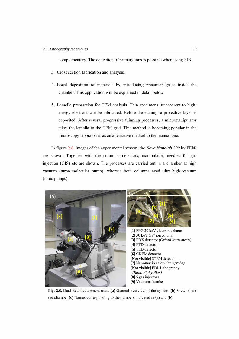
2.1. Lithography techniques 39
complementary. The collection of primary ions is possible when using FIB.
3. Cross section fabrication and analysis.
4. Local deposition of materials by introducing precursor gases inside the
chamber. This application will be explained in detail below.
5. Lamella preparation for TEM analysis. Thin specimens, transparent to high-
energy electrons can be fabricated. Before the etching, a protective layer is
deposited. After several progressive thinning processes, a micromanipulator
takes the lamella to the TEM grid. This method is becoming popular in the
microscopy laboratories as an alternative method to the manual one.
In figure 2.6. images of the experimental system, the Nova Nanolab 200 by FEI®
are shown. Together with the columns, detectors, manipulator, needles for gas
injection (GIS) etc are shown. The processes are carried out in a chamber at high
vacuum (turbo-molecular pump), whereas both columns need ultra-high vacuum
(ionic pumps).
Fig. 2.6. Dual Beam equipment used. (a) General overview of the system. (b) View inside
the chamber (c) Names corresponding to the numbers indicated in (a) and (b).
[2]
[1] [3]
[6]
[7]
[8]
[4] [5] [6]
[7] [8]
[2]
[1]
[1] FEG 30 keV electron column[2] 30 keV Ga+ ion column[3] EDX detector (Oxford Instruments)[4] ETD detector[5] TLD detector[6] CDEM detector[Not visible] STEM detector[7] Nanomanipulator (Omniprobe)[Not visible] EBL Lithography(Raith Elphy Plus)
[8] 5 gas injectors[9] Vacuum chamber
(b)(a)
40 Chapter 2. Experimental techniques
2.1.2.2. Focused electron beam (FEB)
The column used is a Field-Emission-Gun Schottky source, where electrons are
emitted from a field sharp-pointed emitter, held several kilovolts negative potential
relative to a nearby electrode, causing field electron emission. Schottky emitters are
made by coating a tungsten tip with a layer of zirconium oxide, which has the unusual
property of increasing in electrical conductivity at high temperature. The FEG produce
an electron beam smaller in diameter, more coherent and with up to three orders of
magnitude higher brightness than conventional thermionic emitters such as tungsten
filaments. The result is a significant improved signal-to-noise ratio and spatial
resolution.
The electron optics shares similarities with to that of light optics. The FEB
column typically has two lenses, i.e., a condenser lens and an objective lens. The
condenser lens is the probe forming lens, and the objective lens is used to focus the
beam of electrons at the sample surface. A set of apertures of various diameters also
helps in defining the probe size and provides a range of electron currents that may be
used for different applications. Big apertures give high currents and low spatial
resolution. For SEMs the acceleration beam energy is usually in the 1–30 keV range
and the minimum beam diameter is near 1 nm.
To form an image, the beam is scanned, by means of magnetic lenses, along
the sample, row by row. As the electron beam hits each spot on the sample, particles
are emitted by the specimen surface, collected by the detectors to form the SEM image
when convoluting all the spots. Several types of detectors are available in the
equipment. We will only mention the most commonly used: the Everhart-Thornley SE
detector.
As a consequence of the interaction of primary electrons (PE) with matter, both
electrons and photons are emitted by the specimen surface. In figure 2.7(a) we show
those used in our equipment to obtain information. In this section we will only center
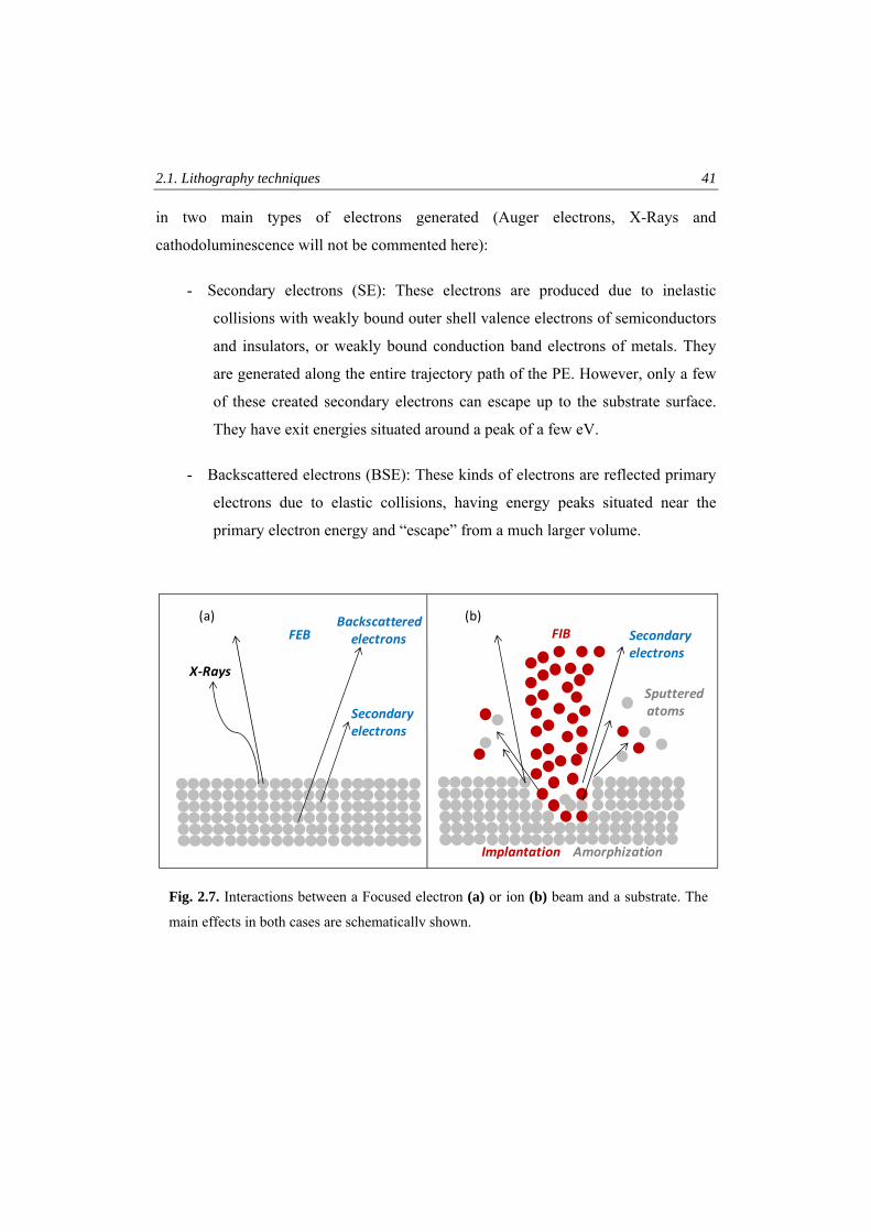
2.1. Lithography techniques 41
in two main types of electrons generated (Auger electrons, X-Rays and
cathodoluminescence will not be commented here):
- Secondary electrons (SE): These electrons are produced due to inelastic
collisions with weakly bound outer shell valence electrons of semiconductors
and insulators, or weakly bound conduction band electrons of metals. They
are generated along the entire trajectory path of the PE. However, only a few
of these created secondary electrons can escape up to the substrate surface.
They have exit energies situated around a peak of a few eV.
- Backscattered electrons (BSE): These kinds of electrons are reflected primary
electrons due to elastic collisions, having energy peaks situated near the
primary electron energy and “escape” from a much larger volume.
Sputteredatoms
Secondaryelectrons
AmorphizationImplantation
FIBBackscatteredelectronsFEB
Secondaryelectrons
X‐Rays
(b)(a)
Fig. 2.7. Interactions between a Focused electron (a) or ion (b) beam and a substrate. The
main effects in both cases are schematically shown.
42 Chapter 2. Experimental techniques
2.1.2.3. Focused ion beam (FIB)
The FIB apparatus is very similar to a SEM. It is composed of three main parts:
the source, the ion optics column, and the stage and beam control. The FIB optics and
stage and beam control are very similar to those for FEB, explained in previous
section. The ion source is a liquid metal source (LMIS), consisting of a reservoir of
liquid gallium, which feeds the liquid metal to a sharpened needle, made of tungsten.
The LMIS has the ability to provide a source of ions of ~ 5 nm in diameter [6], with a
high brightness, typically ~106 A/cm2 sr. The heated Ga flows and wets the W needle.
An electric field applied to the end of the wetted tip causes the liquid Ga to form a
point source on the order of 2-5 nm in diameter at the sample surface. The extraction
voltage can pull Ga from the W tip and efficiently ionize it. Once the ions are
extracted from the LMIS, they are accelerated through a potential (5-30 kV) down the
ion column.
Figure 2.7(b) shows a schematic diagram illustrating some of the possible ion
beam/material interactions that can result from ion bombardment of a solid. Milling
takes place as a result of physical sputtering of the target, when the sputtered particle
receives enough kinetic energy to overcome the surface binding energy of the target
material. Sputtering occurs as the result of a series of elastic collisions where
momentum is transferred from the incident ions to the target atoms within a collision
cascade region. A portion of the ejected atoms may be ionized and collected to either
form an image or be mass analyzed. Inelastic interactions also occur as the result of
ion bombardment. Inelastic scattering events can result in the production of phonons,
plasmons (in metals), and the emission of secondary electrons (SE). Detection of the
emitted SE is the standard mode for imaging in the FIB. If the ion is not backscattered
out of the target surface, it will eventually come to rest, implanted within the target at
some depth below the specimen surface. As a consequence of the high energy of ions,
the amorphization of the material is an important consequence of the FIB process. For
details see reference 7.
2.1. Lithography techniques 43
2.1.2.4. Focused electron/ion beam induced deposition (FEBID/FIBID)
Anyone using an SEM will probably have observed that the surface becomes
contaminated when the beam exposes for some time the same place. This film is
formed from rest of hydrocarbons present in the vacuum system. This undesired effect
can be, however, used to deposit locally a material, if the appropriate gas is adhered to
the surface. This technique is one major application of a Dual Beam system, called
Focused-Electron-Beam-Induced-Deposition (FEBID) and Focused-Ion-Beam-
Induced-Deposition (FIBID), depending on the beam used.
FEBID and FIBID allow local deposition in the targeted place with controllable
lateral size (typical size from 15 nm to 10 µm) and thickness (typically ranging from
10 nm to 10 µm). Amongst applications of FEBID and FIBID deposits, one can cite
the reparation of optical masks and integrated circuits [8], fabrication of three-
dimensional nanostructures [9], deposition of protection layers for lamella preparation
[6], creation of electronic nanodevices [10], fabrication of nanoelectrodes and
nanocontacts [11], transport studies of nanowires [12], deposition of magnetic [13] or
superconductor materials [14], etc. This technique possesses unique advantages to
fabricate nanostructures with respect to more conventional techniques (such as
Electron Beam Lithography, for instance). It is a one step mask-less process, with
resolution around 15 nm (determined by the volume interaction of the beam with the
substrate). Sophisticated structures can be created, on principle on any surface, in a
routine way. To illustrate the advantages with respect to techniques where resist is
necessary, we show in figure 2.8. a comparison between EBL and FEBID/FIBID.
Chapters 5, 6 and 7 in this thesis are dedicated to applications using these techniques.
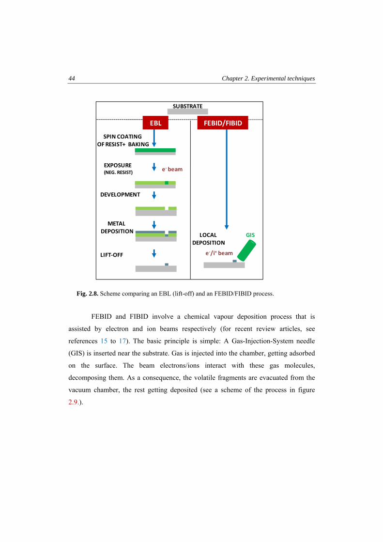
44 Chapter 2. Experimental techniques
FEBID and FIBID involve a chemical vapour deposition process that is
assisted by electron and ion beams respectively (for recent review articles, see
references 15 to 17). The basic principle is simple: A Gas-Injection-System needle
(GIS) is inserted near the substrate. Gas is injected into the chamber, getting adsorbed
on the surface. The beam electrons/ions interact with these gas molecules,
decomposing them. As a consequence, the volatile fragments are evacuated from the
vacuum chamber, the rest getting deposited (see a scheme of the process in figure
2.9.).
Fig. 2.8. Scheme comparing an EBL (lift-off) and an FEBID/FIBID process.
SPIN COATING OF RESIST+ BAKING
DEVELOPMENT
EXPOSURE(NEG. RESIST) e‐ beam
SUBSTRATE
METAL DEPOSITION
e‐/i+ beam
FEBID/FIBIDEBL
LOCALDEPOSITION
GIS
LIFT‐OFF
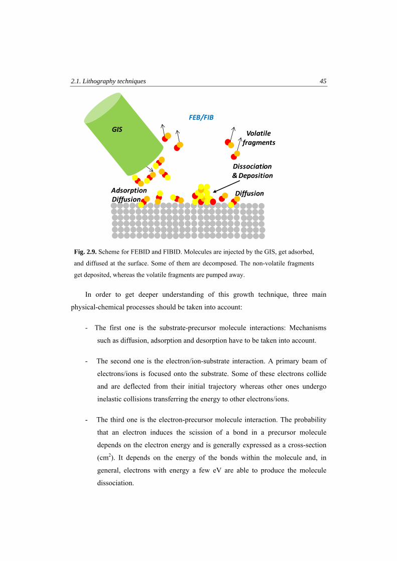
2.1. Lithography techniques 45
In order to get deeper understanding of this growth technique, three main
physical-chemical processes should be taken into account:
- The first one is the substrate-precursor molecule interactions: Mechanisms
such as diffusion, adsorption and desorption have to be taken into account.
- The second one is the electron/ion-substrate interaction. A primary beam of
electrons/ions is focused onto the substrate. Some of these electrons collide
and are deflected from their initial trajectory whereas other ones undergo
inelastic collisions transferring the energy to other electrons/ions.
- The third one is the electron-precursor molecule interaction. The probability
that an electron induces the scission of a bond in a precursor molecule
depends on the electron energy and is generally expressed as a cross-section
(cm2). It depends on the energy of the bonds within the molecule and, in
general, electrons with energy a few eV are able to produce the molecule
dissociation.
FEB/FIB
Diffusion
GIS
Adsorption
Volatilefragments
Diffusion
Dissociation& Deposition
Fig. 2.9. Scheme for FEBID and FIBID. Molecules are injected by the GIS, get adsorbed,
and diffused at the surface. Some of them are decomposed. The non-volatile fragments
get deposited, whereas the volatile fragments are pumped away.
46 Chapter 2. Experimental techniques
Furthermore, three clear deposition regimes have been identified [15-17], which
depend on all the factors described before:
- Electron-limited regime: the growth is limited by the current density and is
independent of the gas flux.
- Precursor-limited regime: the growth is limited by the number of molecules,
coming from the GIS, and arriving on the irradiated area,.
- Diffusion-enhanced regime: the supply of gas molecules for deposition is
dominated by the surface diffusion.
The physical phenomena involved in the deposition are thus complex and models
trying to explain the experimental results take into account factors such as the electron
flux as well as their spatial and energy distribution, the cross section of the precursor
as a function of electron energy, the precursor residence time, the electron-beam
induced heating, etc. An important piece of information has been gained through
Monte Carlo simulations [15-17]. Those simulations have highlighted the important
role played by the generated secondary electrons in the deposition rate and also in the
spatial distribution and resolution of the nanodeposits.
A typical situation for these techniques is to use an organo-metallic gas precursor
for the local deposition. In general, these gases are not fully decomposed, and a
carbonaceous matrix is also present in the deposits. The typical metal content for
deposits by FIBID is around 30-40% atomic, with the rest being mainly carbon,
whereas for FEBID the metal content is usually only around the 15-20 %. Thus, the
main drawback when creating metallic nanostructures with these techniques is the
high carbon percentage present in the deposits, which can influence dramatically the
properties of these nanostructures. Post-growth purification processes are sometimes
used to increase the metallic content [18, 19]. In the case of FIBID, the damage
induced by ions is also an important issue to take into account. These aspects, together
with a higher yield for FIBID with respect to FEBID, are the most relevant differences
between depositing with one or other column. In this thesis we have used three
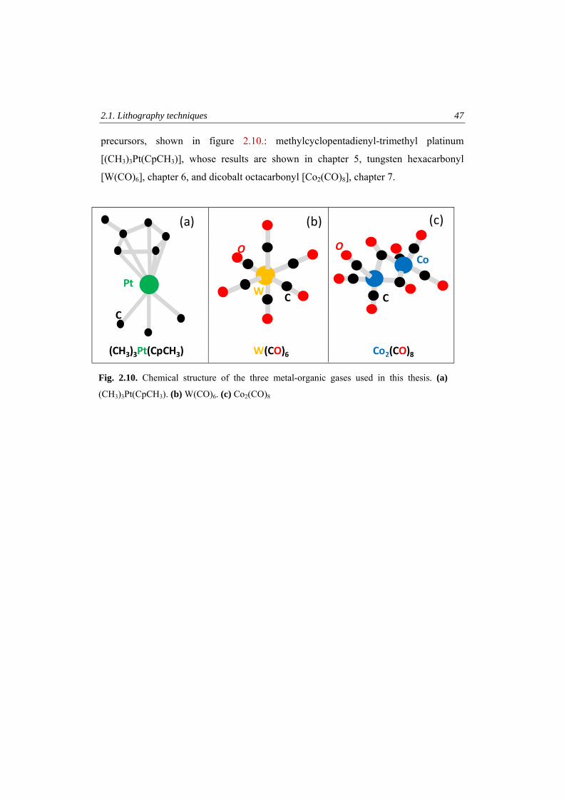
2.1. Lithography techniques 47
precursors, shown in figure 2.10.: methylcyclopentadienyl-trimethyl platinum
[(CH3)3Pt(CpCH3)], whose results are shown in chapter 5, tungsten hexacarbonyl
[W(CO)6], chapter 6, and dicobalt octacarbonyl [Co2(CO)8], chapter 7.
Fig. 2.10. Chemical structure of the three metal-organic gases used in this thesis. (a)
(CH3)3Pt(CpCH3). (b) W(CO)6. (c) Co2(CO)8
(CH3)3Pt(CpCH3)
Pt
C
Co
C
O
Co2(CO)8W(CO)6
W C
O
(b)(a) (c)
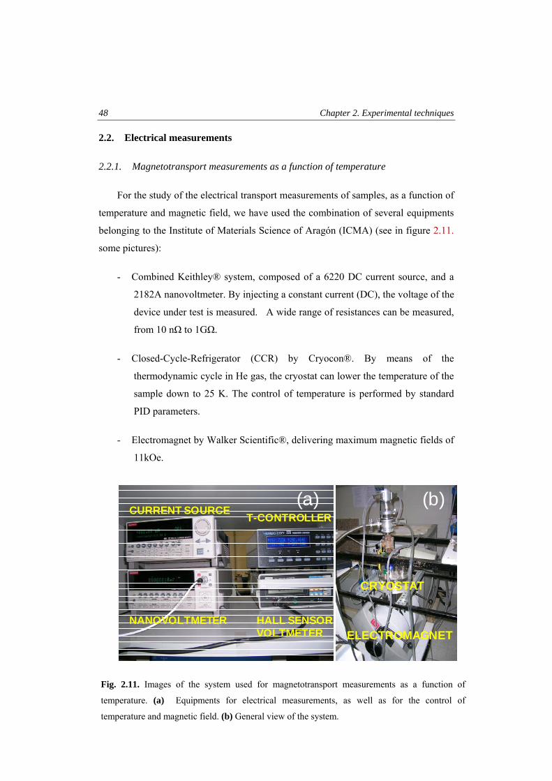
48 Chapter 2. Experimental techniques
2.2. Electrical measurements
2.2.1. Magnetotransport measurements as a function of temperature
For the study of the electrical transport measurements of samples, as a function of
temperature and magnetic field, we have used the combination of several equipments
belonging to the Institute of Materials Science of Aragón (ICMA) (see in figure 2.11.
some pictures):
- Combined Keithley® system, composed of a 6220 DC current source, and a
2182A nanovoltmeter. By injecting a constant current (DC), the voltage of the
device under test is measured. A wide range of resistances can be measured,
from 10 nΩ to 1GΩ.
- Closed-Cycle-Refrigerator (CCR) by Cryocon®. By means of the
thermodynamic cycle in He gas, the cryostat can lower the temperature of the
sample down to 25 K. The control of temperature is performed by standard
PID parameters.
- Electromagnet by Walker Scientific®, delivering maximum magnetic fields of
11kOe.
CURRENT SOURCE
NANOVOLTMETER
T-CONTROLLER
HALL SENSORVOLTMETER ELECTROMAGNET
CRYOSTAT
(b)(a)
Fig. 2.11. Images of the system used for magnetotransport measurements as a function of
temperature. (a) Equipments for electrical measurements, as well as for the control of
temperature and magnetic field. (b) General view of the system.
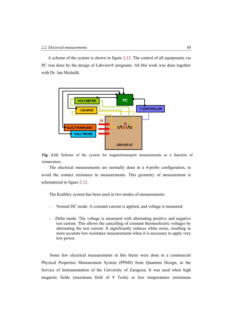
2.2. Electrical measurements 49
A scheme of the system is shown in figure 2.12. The control of all equipments via
PC was done by the design of Labview® programs. All this work was done together
with Dr. Jan Michalik.
The electrical measurements are normally done in a 4-probe configuration, to
avoid the contact resistance in measurements. This geometry of measurement is
schematized in figure 2.12.
The Keithley system has been used in two modes of measurements:
- Normal DC mode: A constant current is applied, and voltage is measured.
- Delta mode: The voltage is measured with alternating positive and negative test current. This allows the cancelling of constant thermoelectric voltages by alternating the test current. It significantly reduces white noise, resulting in more accurate low resistance measurements when it is necessary to apply very low power.
Some few electrical measurements in this thesis were done in a commercial
Physical Properties Measurement System (PPMS) from Quantum Design, in the
Service of Instrumentation of the University of Zaragoza. It was used when high
magnetic fields (maximum field of 9 Tesla) or low temperatures (minimum
PC
R
I SOURCE
VOLTMETER
ELECTROMAGNET
CRYOSTAT
HALL PROBE
T CONTROLLER
H
Fig. 2.12. Scheme of the system for magnetotransport measurements as a function of
temperature.
50 Chapter 2. Experimental techniques
temperature of 300 mK) were necessary, for resistances below ~1MΩ.
2.2.2. “In situ” electrical measurements
Some of the results obtained in the thesis have been done by the combination of
the nanolithography techniques with electrical measurements. The usual approach
followed consists on a study of the devices after having been created or modified.
However, in our case we have also done, in some cases, simultaneous electrical
measurements while the nanostructure was being patterned. For it, two types of special
stages were inside the Dual Beam system (see figure 2.13.):
(i) Four electrical microprobes by Kleindiek®. They are separately moved by a
motor or piezoelectric, till contacted to pads. They are made of tungsten,
have a final diameter of around 1 µm.
(ii) Home-made stage, with eight connections, with the sample contacted by wire-
bonding to a chip carrier, which is loaded in the stage.
The electrical wires are transferred outside the chamber by a port, and connected to the
same Keithley system explained before.
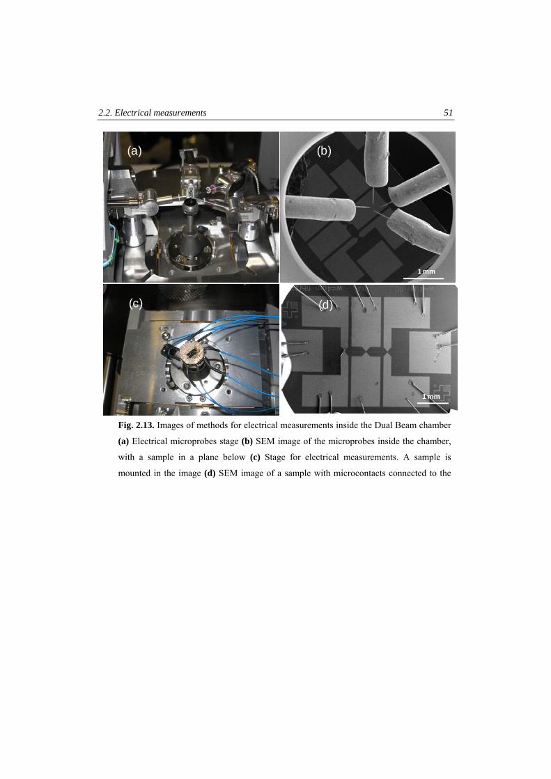
2.2. Electrical measurements 51
Fig. 2.13. Images of methods for electrical measurements inside the Dual Beam chamber
(a) Electrical microprobes stage (b) SEM image of the microprobes inside the chamber,
with a sample in a plane below (c) Stage for electrical measurements. A sample is
mounted in the image (d) SEM image of a sample with microcontacts connected to the
1 mm
(b)(a)
1 mm
(d)(c)
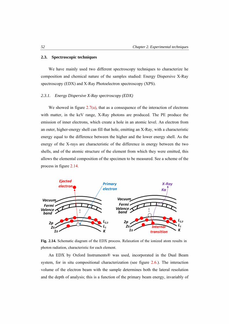
52 Chapter 2. Experimental techniques
2.3. Spectroscopic techniques
We have mainly used two different spectroscopy techniques to characterize he
composition and chemical nature of the samples studied: Energy Dispersive X-Ray
spectroscopy (EDX) and X-Ray Photoelectron spectroscopy (XPS).
2.3.1. Energy Dispersive X-Ray spectroscopy (EDX)
We showed in figure 2.7(a), that as a consequence of the interaction of electrons
with matter, in the keV range, X-Ray photons are produced. The PE produce the
emission of inner electrons, which create a hole in an atomic level. An electron from
an outer, higher-energy shell can fill that hole, emitting an X-Ray, with a characteristic
energy equal to the difference between the higher and the lower energy shell. As the
energy of the X-rays are characteristic of the difference in energy between the two
shells, and of the atomic structure of the element from which they were emitted, this
allows the elemental composition of the specimen to be measured. See a scheme of the
process in figure 2.14.
An EDX by Oxford Instruments® was used, incorporated in the Dual Beam
system, for in situ compositional characterization (see figure 2.6.). The interaction
volume of the electron beam with the sample determines both the lateral resolution
and the depth of analysis; this is a function of the primary beam energy, invariably of
KL12s
L2,32p
1s
Primaryelectron
2p3/2...
Vacuum
Valenceband
Fermi
Ejectedelectron
KL12s
L2,32p
1s
2p3/2...
Vacuum
Valenceband
Fermi
X‐RayKα
Internaltransition
Fig. 2.14. Schematic diagram of the EDX process. Relaxation of the ionized atom results in
photon radiation, characteristic for each element.
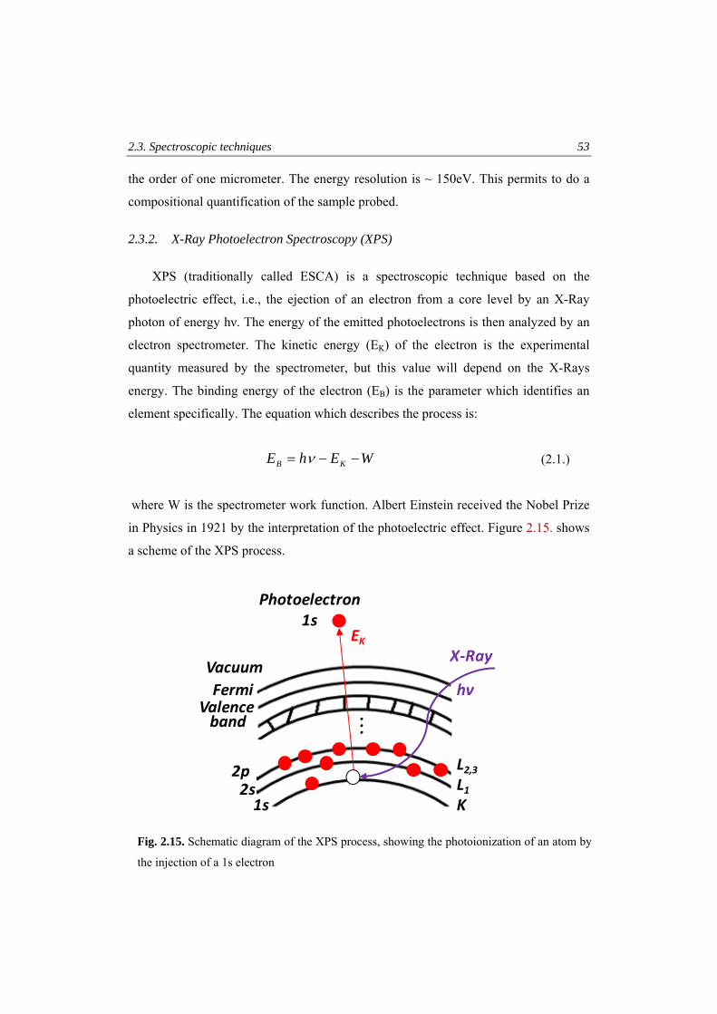
2.3. Spectroscopic techniques 53
the order of one micrometer. The energy resolution is ~ 150eV. This permits to do a
compositional quantification of the sample probed.
2.3.2. X-Ray Photoelectron Spectroscopy (XPS)
XPS (traditionally called ESCA) is a spectroscopic technique based on the
photoelectric effect, i.e., the ejection of an electron from a core level by an X-Ray
photon of energy hν. The energy of the emitted photoelectrons is then analyzed by an
electron spectrometer. The kinetic energy (EK) of the electron is the experimental
quantity measured by the spectrometer, but this value will depend on the X-Rays
energy. The binding energy of the electron (EB) is the parameter which identifies an
element specifically. The equation which describes the process is:
WEhE KB −−= ν (2.1.)
where W is the spectrometer work function. Albert Einstein received the Nobel Prize
in Physics in 1921 by the interpretation of the photoelectric effect. Figure 2.15. shows
a scheme of the XPS process.
KL12s
L2,32p
1s
Vacuum
Valenceband
Fermi
Photoelectron1s
EK
hν
X‐Ray
...
Fig. 2.15. Schematic diagram of the XPS process, showing the photoionization of an atom by
the injection of a 1s electron
54 Chapter 2. Experimental techniques
For these experiments we used an Axis Ultra DLD equipment by Kratos® , in the
INA. A monochromatic Al kα X-Ray source was used, with exciting energy
hν=1486.6eV. The sampling depth of X-ray is in the micrometric level, while only
those photoelectrons from the outermost, ~10 nm or less, escape without energy loss.
These electrons are those used for quantitative quantification; XPS is, thus a surface-
sensitive technique. An in-depth study can be performed since the equipment
incorporates a 5kV- Ar+ gun, which progressively etches layers of material, which are
consequently probed by XPS. A hemispherical detector analyzes the electron energy.
The experiments require ultra-high vacuum conditions (ionic pump).
Due to the difficulty in focusing X-Rays, the effective minimum area probed in
the equipment is approximately 30 × 30 µm2. The high resolution of the equipment
(maximum = 0.25 eV) permits to distinguish the valence state of the atoms composing
the sample.
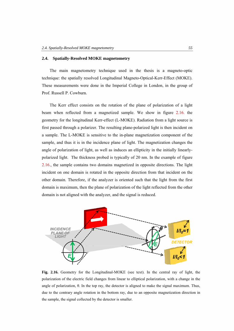
2.4. Spatially-Resolved MOKE magnetometry 55
2.4. Spatially-Resolved MOKE magnetometry
The main magnetometry technique used in the thesis is a magneto-optic
technique: the spatially resolved Longitudinal Magneto-Optical-Kerr-Effect (MOKE).
These measurements were done in the Imperial College in London, in the group of
Prof. Russell P. Cowburn.
The Kerr effect consists on the rotation of the plane of polarization of a light
beam when reflected from a magnetized sample. We show in figure 2.16. the
geometry for the longitudinal Kerr-effect (L-MOKE). Radiation from a light source is
first passed through a polarizer. The resulting plane-polarized light is then incident on
a sample. The L-MOKE is sensitive to the in-plane magnetization component of the
sample, and thus it is in the incidence plane of light. The magnetization changes the
angle of polarization of light, as well as induces an ellipticity in the initially linearly-
polarized light. The thickness probed is typically of 20 nm. In the example of figure
2.16., the sample contains two domains magnetized in opposite directions. The light
incident on one domain is rotated in the opposite direction from that incident on the
other domain. Therefore, if the analyzer is oriented such that the light from the first
domain is maximum, then the plane of polarization of the light reflected from the other
domain is not aligned with the analyzer, and the signal is reduced.
Fig. 2.16. Geometry for the Longitudinal-MOKE (see text). In the central ray of light, the
polarization of the electric field changes from linear to elliptical polarization, with a change in the
angle of polarization, θ. In the top ray, the detector is aligned to make the signal maximum. Thus,
due to the contrary angle rotation in the bottom ray, due to an opposite magnetization direction in
the sample, the signal collected by the detector is smaller.
E
E
θ I/I0=1
DETECTOR
INCIDENCEPLANE OF
LIGHT
I/I0<1
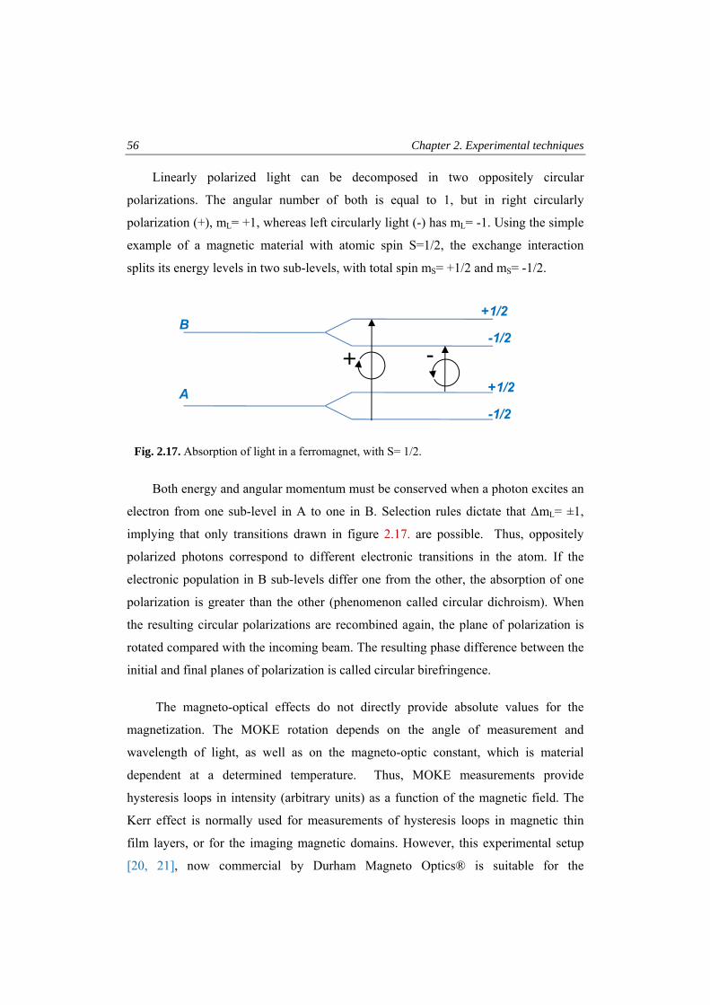
56 Chapter 2. Experimental techniques
Linearly polarized light can be decomposed in two oppositely circular
polarizations. The angular number of both is equal to 1, but in right circularly
polarization (+), mL= +1, whereas left circularly light (-) has mL= -1. Using the simple
example of a magnetic material with atomic spin S=1/2, the exchange interaction
splits its energy levels in two sub-levels, with total spin mS= +1/2 and mS= -1/2.
Both energy and angular momentum must be conserved when a photon excites an
electron from one sub-level in A to one in B. Selection rules dictate that ΔmL= ±1,
implying that only transitions drawn in figure 2.17. are possible. Thus, oppositely
polarized photons correspond to different electronic transitions in the atom. If the
electronic population in B sub-levels differ one from the other, the absorption of one
polarization is greater than the other (phenomenon called circular dichroism). When
the resulting circular polarizations are recombined again, the plane of polarization is
rotated compared with the incoming beam. The resulting phase difference between the
initial and final planes of polarization is called circular birefringence.
The magneto-optical effects do not directly provide absolute values for the
magnetization. The MOKE rotation depends on the angle of measurement and
wavelength of light, as well as on the magneto-optic constant, which is material
dependent at a determined temperature. Thus, MOKE measurements provide
hysteresis loops in intensity (arbitrary units) as a function of the magnetic field. The
Kerr effect is normally used for measurements of hysteresis loops in magnetic thin
film layers, or for the imaging magnetic domains. However, this experimental setup
[20, 21], now commercial by Durham Magneto Optics® is suitable for the
Fig. 2.17. Absorption of light in a ferromagnet, with S= 1/2.
A
B+1/2
+1/2
-1/2
-1/2
+ -
2.4. Spatially-Resolved MOKE magnetometry 57
measurement of magnetic nanometric structures. A diode-pumped solid state laser
(λ=532 nm) with a diameter of about 5 µm (FWHM) is used as probe. A CCD camera
is used for pre-alignment of the nanometric structure, located on a substrate. The final
alignment is done by performing a reflectivity map of the zone of interest. A motor
permits to move the stage with a resolution of 50 nm. A quadruple is used for applying
AC magnetic fields (1-27Hz), with Hmax~400 Oe. The system is the state-of-the-art-
MOKE instrument, having, for instance, a sensitivity for permalloy S=6×10-12 emu at
room temperature [21] (in a SQUID magnetometer S ~10-8- 10-9 emu). This high
sensitivity permits to measure hysteresis loops in sub-micrometric & sub-λ
nanomagnets. As the diameter of the laser is bigger than, at least, one of the
dimensions of the nanostructure probed, a dilution factor is present in the MOKE
signal with respect to the bulk material.
58 Chapter 2. Experimental techniques
2.5. Atomic Force Microscopy
In previous sections we have cited two main microscopy techniques used for this
work: the optical microscope, allowing the observation of structures with sizes slightly
below one micron, and the scanning electron microscope, which can resolve objects
around 1 nm in size.
In this section, we will comment some aspects of another microscope used, with
resolution of fractions of a nanometer: the Atomic Force Microscope (AFM). AFM is
a type of scanning probe microscope (as its father, the Scanning Tunneling
Microscope), based on the interaction of a sharp tip with the surface sample, when it is
brought into proximity to the surface. The tip is the end of a microscopic cantilever,
used to scan the specimen surface. The cantilever is typically silicon or silicon nitride
with a tip radius of curvature on the order of nanometers. The forces between the tip
and the sample lead to a deflection of the cantilever, which can be modeled with the
Hooke's law. The typical AFM forces are mechanical contact force, Van der Waals
force, capillary forces, electrostatic forces, magnetic force (MFM) etc. Typically, the
deflection is measured using a laser spot reflected from the top surface of the
cantilever into an array of photodiodes.
The AFM images were performed in the Imperial College in London, with a
Veeco® AFM. The PHD student Liam O’Brien, whose thesis director is Prof. Russell
P. Cowburn, did a part of the measurements. Contact mode was used for imaging,
where the force between the tip and the surface is kept constant during scanning by
maintaining a constant deflection. The tip deflection is used as a feedback signal,
which is used to form an image of the structure probed.
Some clear advantages of AFM with respect to the SEM can be named, such as a
better spatial resolution, the measurements do not require vacuum conditions, a true
three-dimensional surface profile is obtained, and there are not charging-effects
problems with insulator samples. However, there exist important disadvantages of
AFM compared with SEM. The SEM can image an area on the order of mm × mm,
2.5. Atomic Force Microscopy 59
with a depth of field on the order of mm. The AFM can only image a maximum height
on the order of microns, and a maximum scanning area of a few µm2. Besides, image
artifacts are common, especially if an incorrect choice of tip for the required resolution
is done. The significant lower speed in the image is also an important drawback, as
well as the possible hysteresis in the piezoelectric. We should cite for completeness
that AFM is also used as a tool for nano-patterning, by local oxidation, dip-pen
nanolithography, etc.
60 Chapter 2. Experimental techniques
2.6. Other techniques
In the thesis, some results will be presented with other techniques different from
those explained before, and should also be mentioned. The person in charge of the
measurements is cited in the text when a particular result is presented, in following
chapters.
Pulsed Laser Deposition, PLD (INA): Fe3O4 thin films were epitaxially grown on
MgO (001) substrates. A KrF pulsed laser produces an ablation in a Fe3O4 target,
depositing stochiometrically the iron oxide on the substrate.
High Resolution X-Ray Diffraction, HR-XRD (INA): Structural characterization
of thin films. Determination of the degree of crystallinity of a film grown on a
substrate.
Superconducting quantum interference device, SQUID magnetometer (Scientific
services of University of Zaragoza): A constant current passes through two in-parallel
Josephson junctions. The applied voltage oscillates with the changes in the phase of
the two junctions, which depend upon the change in magnetic flux. This results in a
highly sensitive magnetometer.
High-Resolution Transmission Electron Microscope, HRTEM (Scientific
Services of the University of Barcelona): 200 kV- electrons are accelerated, being
transmitted through a thin sample (~100 nm). The image formed, consequence of the
diffraction of electrons with the material, can be transformed to the real space,
resulting in an image of the crystallographic structure of a sample at an atomic scale.
Scanning-Tunneling-Spectroscopy, STS (University Autonóma of Madrid, group
of Prof. Sebastián Vieira): The local density of electronic states of a surface is probed
at the atomic scale, by measuring the tunneling differential conductance between a
STM tip and a sample at low temperatures.
Chapter 3
Magnetotransport properties of
epitaxial Fe3O4 thin films
In this chapter we will show the magnetotransport properties of epitaxial Fe3O4 thin
films [grown on MgO (001)]. A broad characterization has been performed, studying
systematically, for several film thicknesses and as a function of temperature, the
resistivity, magnetoresistance in different geometries, Hall effect and Planar Hall
effect. Most of the measurements are substantially influenced by the presence of the
Antiphase Boundaries, especially for ultra-thin films. In the case of the Anomalous
Hall effect, an experimental evidence of the universal character of this phenomenon
was demonstrated.
The growth of the films was performed by J. Orna, being matter of her Ph. D. Thesis.
62 Chapter 3.Magnetotransport properties of epitaxial Fe3O4 thin films
3.1. Introduction
3.1.1. General properties of Fe3O4
Magnetite, Fe3O4 is the first magnetic material referred in the history of
humankind. Its magnetic properties were reported in the Chinese book of the Devil
Master, in the 4th century BC. This iron oxide is the magnetic mineral contained in
lodestone, from which first compasses for navigation were made. In spite of this long
perid, physics of magnetite still has a lot of open unresolved aspects.
Magnetite is magnetic at room temperature, being ferrimagnetic, with a Curie
temperature of 858 K [1]. It belongs to the cubic ferrite family: Fe2+O2-·(2Fe3+3O2-),
with an inverse spinel crystallographic structure (lattice constant=8.397 Å). This
structure (Fd3m space group) consist of a face-centered-cubic (FCC) oxygen lattice,
with Fe3+ ions filling 1/8 of the available tetrahedral sites (A sites), and equal amounts
of Fe2+ and Fe3+ ions filling half of the available octahedral site (B sites), see figure
3.1(a).
The spin moments of all the Fe3+ ions on B sites are ferromagnetically aligned
and in opposite direction to the Fe3+ occupying the A sites. Therefore the magnetic
moments of all Fe3+ cancel out, resulting in a zero contribution to the overall
magnetization of the solid. However, all the divalent ions are ferromagnetically
aligned parallel, providing a net magnetization of approximately 4 µB/f.u. Several
magnetic exchange interactions are present in Fe3O4, which are detailed in figure
3.1(b).
The conduction in magnetite has been extensively studied and modeled. In a
simple picture, as a consequence of the double-exchange (ferromagnetic) interaction
existing between Fe2+ and Fe3+ in B sites, the additional spin-down electron can hop
between neighboring B-sites, resulting in a high conductivity, and an intermediate
valence of Fe2.56+. Around 120 K (Tv), a first-order phase transition occurs, the so
called Verwey transition [2]. At this transition, the structure distorts from cubic
symmetry [3, 4], and a charge ordering occurs at the B sites, reducing the conductivity
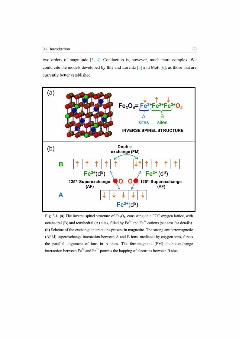
3.1. Introduction 63
two orders of magnitude [3, 4]. Conduction is, however, much more complex. We
could cite the models developed by Ihle and Lorentz [5] and Mott [6], as those that are
currently better established.
Fig. 3.1. (a) The inverse spinel structure of Fe3O4, consisting on a FCC oxygen lattice, with
octahedral (B) and tetrahedral (A) sites, filled by Fe2+ and Fe3+ cations (see text for details).
(b) Scheme of the exchange interactions present in magnetite. The strong antiferromagnetic
(AFM) superexchange interaction between A and B ions, mediated by oxygen ions, forces
the parallel alignment of ions in A sites. The ferromagnetic (FM) double-exchange
interaction between Fe2+ and Fe3+ permits the hopping of electrons between B sites.
Fe3O4= Fe3+Fe2+Fe3+O4
Asites
INVERSE SPINEL STRUCTURE
Bsites
Fe2+ (d6)Fe3+(d5)
Fe3+(d5)
Double exchange (FM)
B
A
125º- Superexchange (AF)
125º- Superexchange (AF)
O O
(a)
(b)
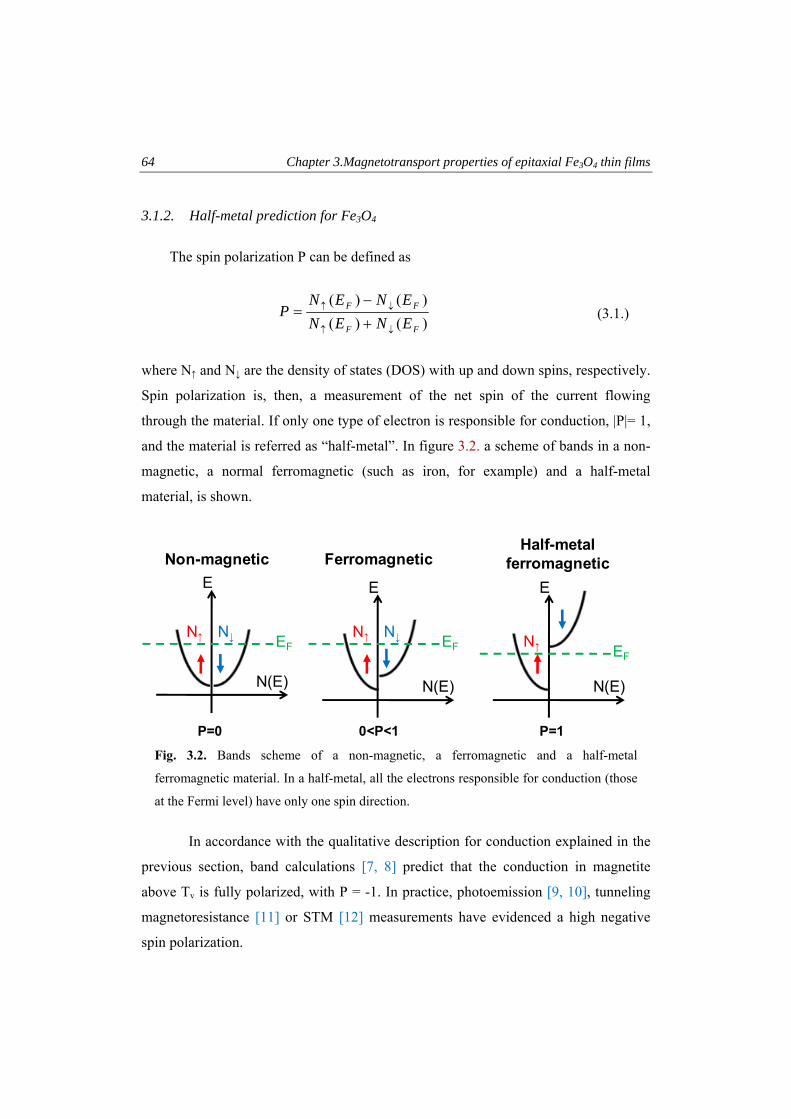
64 Chapter 3.Magnetotransport properties of epitaxial Fe3O4 thin films
3.1.2. Half-metal prediction for Fe3O4
The spin polarization P can be defined as
)()()()(
FF
FF
ENENENEN
P↓↑
↓↑
+−
= (3.1.)
where N↑ and N↓ are the density of states (DOS) with up and down spins, respectively.
Spin polarization is, then, a measurement of the net spin of the current flowing
through the material. If only one type of electron is responsible for conduction, |P|= 1,
and the material is referred as “half-metal”. In figure 3.2. a scheme of bands in a non-
magnetic, a normal ferromagnetic (such as iron, for example) and a half-metal
material, is shown.
In accordance with the qualitative description for conduction explained in the
previous section, band calculations [7, 8] predict that the conduction in magnetite
above Tv is fully polarized, with P = -1. In practice, photoemission [9, 10], tunneling
magnetoresistance [11] or STM [12] measurements have evidenced a high negative
spin polarization.
EFN↑ N↓
Non-magneticE
N(E)
P=0
N↑ N↓ EF
Ferromagnetic
E
N(E)
0<P<1
N↑ EF
Half-metal ferromagnetic
E
N(E)
P=1
Fig. 3.2. Bands scheme of a non-magnetic, a ferromagnetic and a half-metal
ferromagnetic material. In a half-metal, all the electrons responsible for conduction (those
at the Fermi level) have only one spin direction.
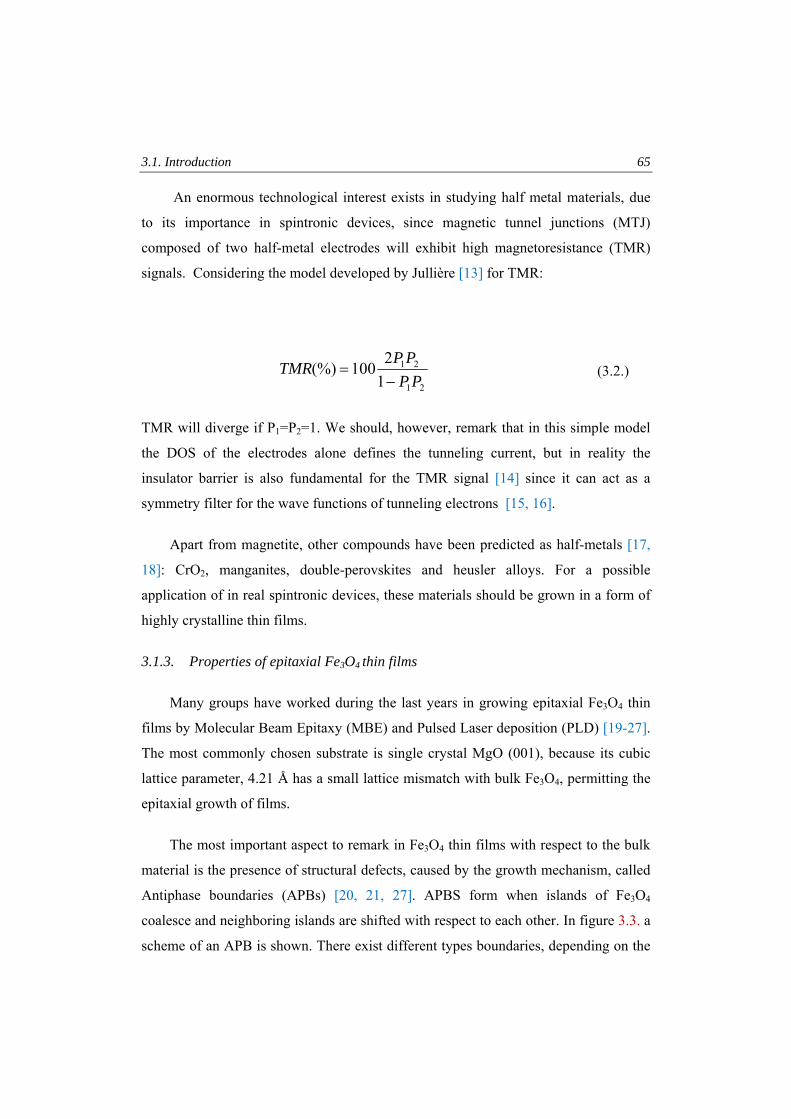
3.1. Introduction 65
An enormous technological interest exists in studying half metal materials, due
to its importance in spintronic devices, since magnetic tunnel junctions (MTJ)
composed of two half-metal electrodes will exhibit high magnetoresistance (TMR)
signals. Considering the model developed by Jullière [13] for TMR:
21
21
12100(%)
PPPPTMR
−= (3.2.)
TMR will diverge if P1=P2=1. We should, however, remark that in this simple model
the DOS of the electrodes alone defines the tunneling current, but in reality the
insulator barrier is also fundamental for the TMR signal [14] since it can act as a
symmetry filter for the wave functions of tunneling electrons [15, 16].
Apart from magnetite, other compounds have been predicted as half-metals [17,
18]: CrO2, manganites, double-perovskites and heusler alloys. For a possible
application of in real spintronic devices, these materials should be grown in a form of
highly crystalline thin films.
3.1.3. Properties of epitaxial Fe3O4 thin films
Many groups have worked during the last years in growing epitaxial Fe3O4 thin
films by Molecular Beam Epitaxy (MBE) and Pulsed Laser deposition (PLD) [19-27].
The most commonly chosen substrate is single crystal MgO (001), because its cubic
lattice parameter, 4.21 Å has a small lattice mismatch with bulk Fe3O4, permitting the
epitaxial growth of films.
The most important aspect to remark in Fe3O4 thin films with respect to the bulk
material is the presence of structural defects, caused by the growth mechanism, called
Antiphase boundaries (APBs) [20, 21, 27]. APBS form when islands of Fe3O4
coalesce and neighboring islands are shifted with respect to each other. In figure 3.3. a
scheme of an APB is shown. There exist different types boundaries, depending on the
66 Chapter 3.Magnetotransport properties of epitaxial Fe3O4 thin films
vector shift present. For details of APBs see references 21 and 27.
These structural defects play a major role in the properties of magnetite thin films,
mainly due to the superexchange AF interactions between spins surrounding the
boundary. The important increase of resistivity [22], the lack of saturation in the
magnetization [27], or a higher magnetoresistance effect than in single crystals [20,
26, 28], as a consequence of the spin-polarized transport, are caused by APBs. It is
important to point out that spin-resolved photoemission studies in thin films, show that
APBs do not seem to reduce significantly the spin polarization in films [29].
Fig. 3.3. Schematic representation of an APB in Fe3O4 formed in a MgO (001) substrate.
When right and left iron oxide islands coalesce while growing, a loss of periodicity can
occur, forming a boundary.
Fe O=[110]
[110]
MgO(001)
3.2. Experimental details 67
3.2. Experimental details
3.2.1. Growth of the films
The Fe3O4 target was prepared from Fe powder by solid-sate reaction [30]. Fe3O4
thin films were grown [31] on MgO (001) substrates by PLD using a KrF excimer
laser with 248 nm wavelength, 10 Hz repetition rate and 3×10⁹ W/cm2 irradiance. The
base pressure in the deposition chamber was lower than 10-8 Torr, and the substrate
was kept in vacuum at ≈400 ºC during laser ablation of the target.
3.2.2. Types of electrical measurement: Van der Paw and Optical lithography
The magnetotransport measurements were performed in the combined closed
cycle refrigerator- electromagnet-Keithley system explained in section 2. Basically, all
the work that will be exposed below comprises two types of measurements:
- As a function of the thin film thickness, at room temperature: 5 × 5 mm2
samples were deposited, being measured by the Van Der Pauw technique
[32] (current // [001] or // [110], depending on if longitudinal or
transversal resistivity components is measured) after wire-bonding to the
corners of the sample (see figure 3.4(a1) and (a2))
- As a function of temperature, for selected thicknesses= 40 and 20 nm: An
optical lithography process was carried out in 0.5 × 0.5 inch2 samples
(current // (001), see figure 3.4(b) and section 2.1.1.), since the big
resistance values for Fe3O4 at low temperatures (especially below Tv)
would do unfeasible the measurements of transversal voltages (Hall and
Planar Hall effect) with the Van Der Paw method.
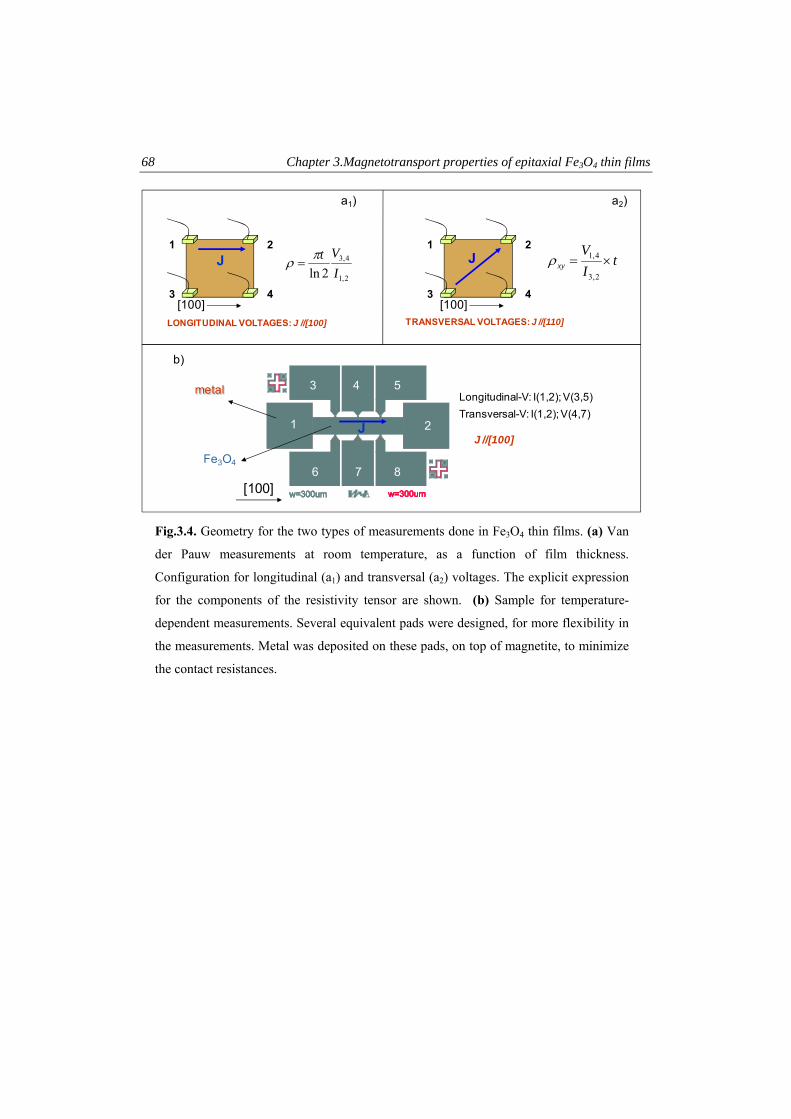
68 Chapter 3.Magnetotransport properties of epitaxial Fe3O4 thin films
Fig.3.4. Geometry for the two types of measurements done in Fe3O4 thin films. (a) Van
der Pauw measurements at room temperature, as a function of film thickness.
Configuration for longitudinal (a1) and transversal (a2) voltages. The explicit expression
for the components of the resistivity tensor are shown. (b) Sample for temperature-
dependent measurements. Several equivalent pads were designed, for more flexibility in
the measurements. Metal was deposited on these pads, on top of magnetite, to minimize
the contact resistances.
2,1
4,3
2ln IVtπρ =
metal
Fe3O4
1 2
3 4 5
6 7 8
Longitudinal-V: I(1,2); V(3,5)Transversal-V: I(1,2); V(4,7)
[100]
tIV
xy ×=2,3
4,1ρ1 2
3 4
J1 2
3 4
J
LONGITUDINAL VOLTAGES: J //[100] TRANSVERSAL VOLTAGES: J //[110]
[100] [100]
a1) a2)
J //[100]
b)
J
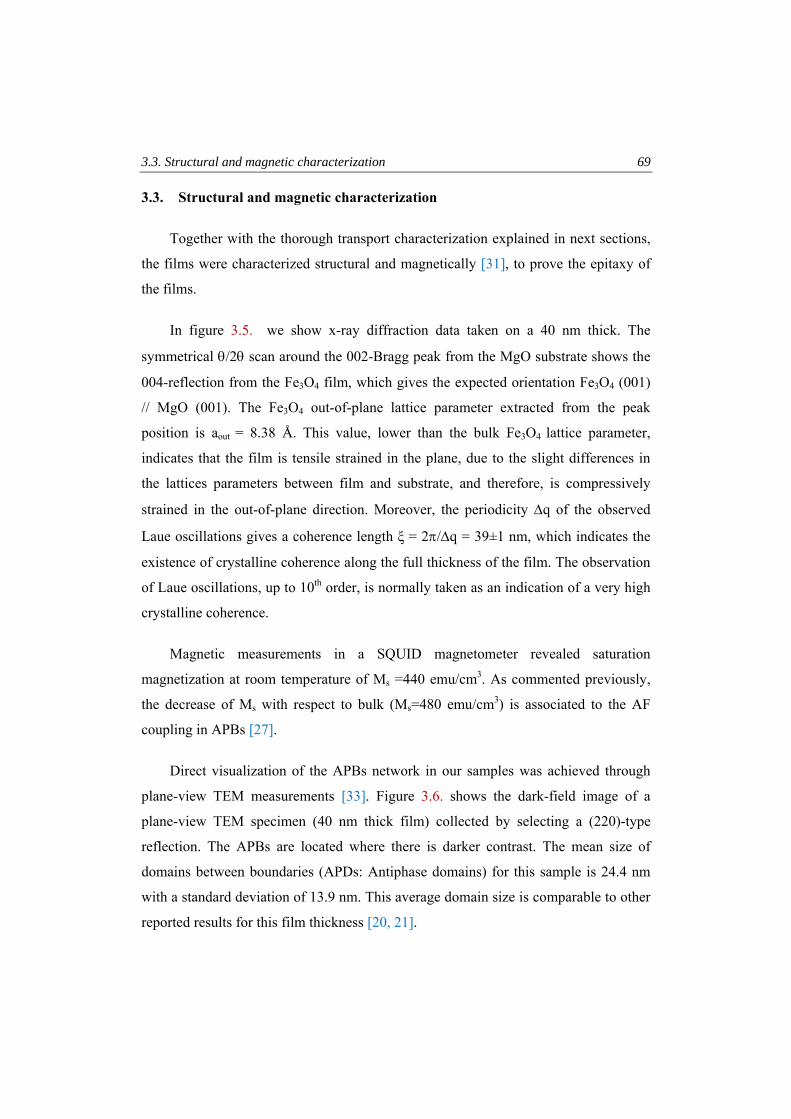
3.3. Structural and magnetic characterization 69
3.3. Structural and magnetic characterization
Together with the thorough transport characterization explained in next sections,
the films were characterized structural and magnetically [31], to prove the epitaxy of
the films.
In figure 3.5. we show x-ray diffraction data taken on a 40 nm thick. The
symmetrical θ/2θ scan around the 002-Bragg peak from the MgO substrate shows the
004-reflection from the Fe3O4 film, which gives the expected orientation Fe3O4 (001)
// MgO (001). The Fe3O4 out-of-plane lattice parameter extracted from the peak
position is aout = 8.38 Å. This value, lower than the bulk Fe3O4 lattice parameter,
indicates that the film is tensile strained in the plane, due to the slight differences in
the lattices parameters between film and substrate, and therefore, is compressively
strained in the out-of-plane direction. Moreover, the periodicity Δq of the observed
Laue oscillations gives a coherence length ξ = 2π/Δq = 39±1 nm, which indicates the
existence of crystalline coherence along the full thickness of the film. The observation
of Laue oscillations, up to 10th order, is normally taken as an indication of a very high
crystalline coherence.
Magnetic measurements in a SQUID magnetometer revealed saturation
magnetization at room temperature of Ms =440 emu/cm3. As commented previously,
the decrease of Ms with respect to bulk (Ms=480 emu/cm3) is associated to the AF
coupling in APBs [27].
Direct visualization of the APBs network in our samples was achieved through
plane-view TEM measurements [33]. Figure 3.6. shows the dark-field image of a
plane-view TEM specimen (40 nm thick film) collected by selecting a (220)-type
reflection. The APBs are located where there is darker contrast. The mean size of
domains between boundaries (APDs: Antiphase domains) for this sample is 24.4 nm
with a standard deviation of 13.9 nm. This average domain size is comparable to other
reported results for this film thickness [20, 21].
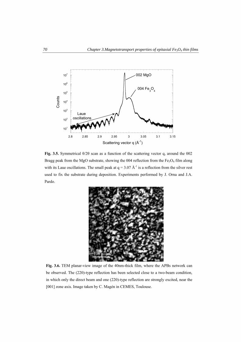
70 Chapter 3.Magnetotransport properties of epitaxial Fe3O4 thin films
Fig. 3.6. TEM planar-view image of the 40nm-thick film, where the APBs network can
be observed. The (220)-type reflection has been selected close to a two-beam condition,
in which only the direct beam and one (220)-type reflection are strongly excited, near the
[001] zone axis. Image taken by C. Magén in CEMES, Toulouse.
101
102
103
104
105
106
107
2.8 2.85 2.9 2.95 3 3.05 3.1 3.15
Cou
nts
Scattering vector q (Å-1)
002 MgO
004 Fe3O
4
Laue oscillations
0
100
200
300
400
500
-180 -135 -90 -45 0 45 90 135 180
Cou
nts
φ (degrees)
(311) Fe3O
4
Fig. 3.5. Symmetrical θ/2θ scan as a function of the scattering vector q, around the 002
Bragg peak from the MgO substrate, showing the 004 reflection from the Fe3O4 film along
with its Laue oscillations. The small peak at q = 3.07 Å-1 is a reflection from the silver rest
used to fix the substrate during deposition. Experiments performed by J. Orna and J.A.
Pardo.
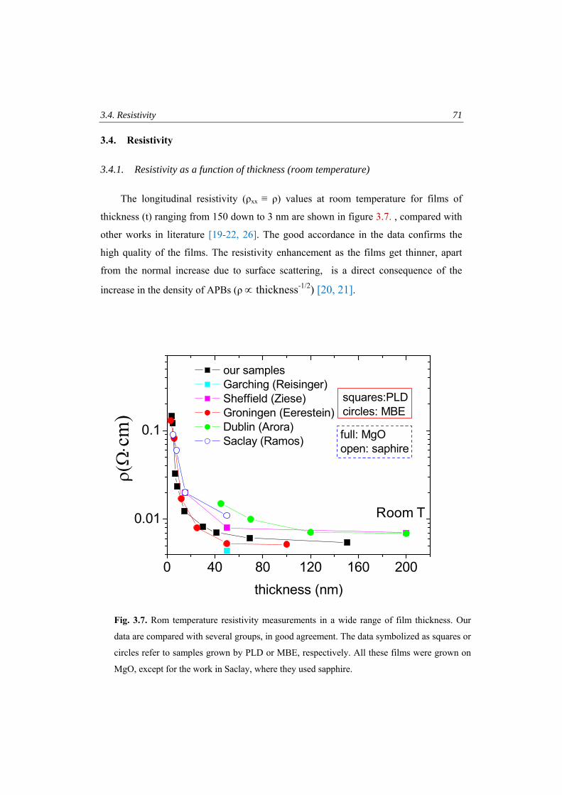
3.4. Resistivity 71
3.4. Resistivity
3.4.1. Resistivity as a function of thickness (room temperature)
The longitudinal resistivity (ρxx ≡ ρ) values at room temperature for films of
thickness (t) ranging from 150 down to 3 nm are shown in figure 3.7. , compared with
other works in literature [19-22, 26]. The good accordance in the data confirms the
high quality of the films. The resistivity enhancement as the films get thinner, apart
from the normal increase due to surface scattering, is a direct consequence of the
increase in the density of APBs (ρ ∝ thickness-1/2) [20, 21].
0 40 80 120 160 200
0.01
0.1
our samples Garching (Reisinger) Sheffield (Ziese) Groningen (Eerestein) Dublin (Arora) Saclay (Ramos)
ρ(Ω
⋅cm
)
thickness (nm)
squares:PLDcircles: MBE
full: MgOopen: saphire
Room T
Fig. 3.7. Rom temperature resistivity measurements in a wide range of film thickness. Our
data are compared with several groups, in good agreement. The data symbolized as squares or
circles refer to samples grown by PLD or MBE, respectively. All these films were grown on
MgO, except for the work in Saclay, where they used sapphire.
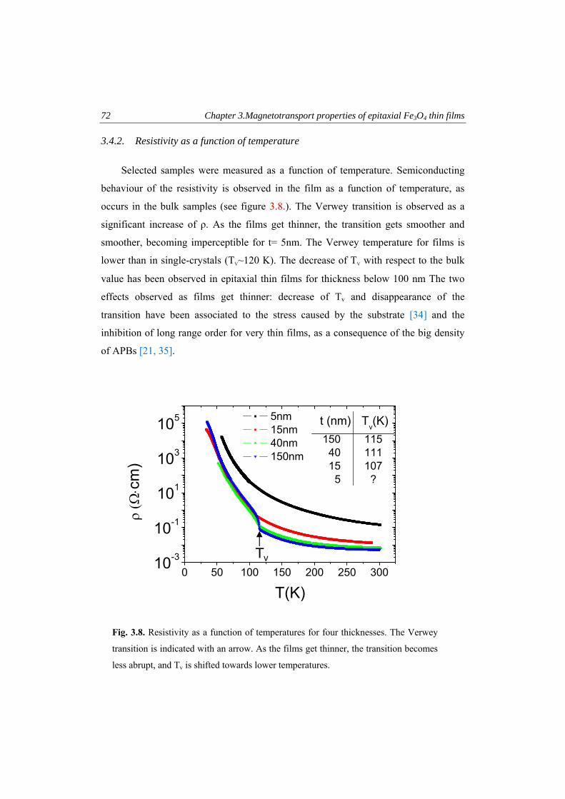
72 Chapter 3.Magnetotransport properties of epitaxial Fe3O4 thin films
3.4.2. Resistivity as a function of temperature
Selected samples were measured as a function of temperature. Semiconducting
behaviour of the resistivity is observed in the film as a function of temperature, as
occurs in the bulk samples (see figure 3.8.). The Verwey transition is observed as a
significant increase of ρ. As the films get thinner, the transition gets smoother and
smoother, becoming imperceptible for t= 5nm. The Verwey temperature for films is
lower than in single-crystals (TV~120 K). The decrease of TV with respect to the bulk
value has been observed in epitaxial thin films for thickness below 100 nm The two
effects observed as films get thinner: decrease of Tv and disappearance of the
transition have been associated to the stress caused by the substrate [34] and the
inhibition of long range order for very thin films, as a consequence of the big density
of APBs [21, 35].
Fig. 3.8. Resistivity as a function of temperatures for four thicknesses. The Verwey
transition is indicated with an arrow. As the films get thinner, the transition becomes
less abrupt, and Tv is shifted towards lower temperatures.
0 50 100 150 200 250 30010-3
10-1
101
103
105
t (nm) Tv(K)
ρ (Ω
⋅cm
)
T(K)
5nm 15nm 40nm 150nm
150 40 15 5
115111107 ?
Tv
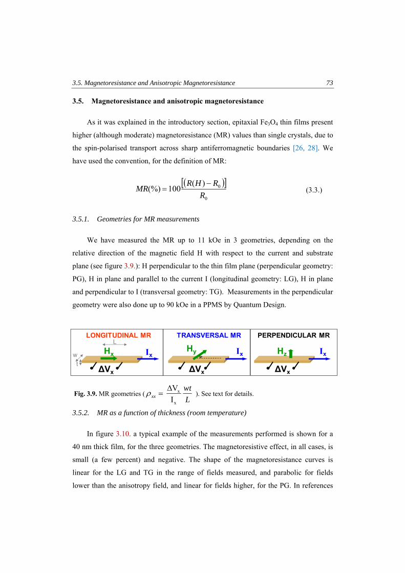
3.5. Magnetoresistance and Anisotropic Magnetoresistance 73
3.5. Magnetoresistance and anisotropic magnetoresistance
As it was explained in the introductory section, epitaxial Fe3O4 thin films present
higher (although moderate) magnetoresistance (MR) values than single crystals, due to
the spin-polarised transport across sharp antiferromagnetic boundaries [26, 28]. We
have used the convention, for the definition of MR:
( )[ ]0
0)(100(%)
RRHR
MR−
= (3.3.)
3.5.1. Geometries for MR measurements
We have measured the MR up to 11 kOe in 3 geometries, depending on the
relative direction of the magnetic field H with respect to the current and substrate
plane (see figure 3.9.): H perpendicular to the thin film plane (perpendicular geometry:
PG), H in plane and parallel to the current I (longitudinal geometry: LG), H in plane
and perpendicular to I (transversal geometry: TG). Measurements in the perpendicular
geometry were also done up to 90 kOe in a PPMS by Quantum Design.
3.5.2. MR as a function of thickness (room temperature)
In figure 3.10. a typical example of the measurements performed is shown for a
40 nm thick film, for the three geometries. The magnetoresistive effect, in all cases, is
small (a few percent) and negative. The shape of the magnetoresistance curves is
linear for the LG and TG in the range of fields measured, and parabolic for fields
lower than the anisotropy field, and linear for fields higher, for the PG. In references
Fig. 3.9. MR geometries (Lwt
xxx
x
IV Δ=ρ ). See text for details.
Ix
LONGITUDINAL MR TRANSVERSAL MR PERPENDICULAR MR
Hx Hz
ΔVx ΔVx ΔVx
Ix IxHy
tw
L
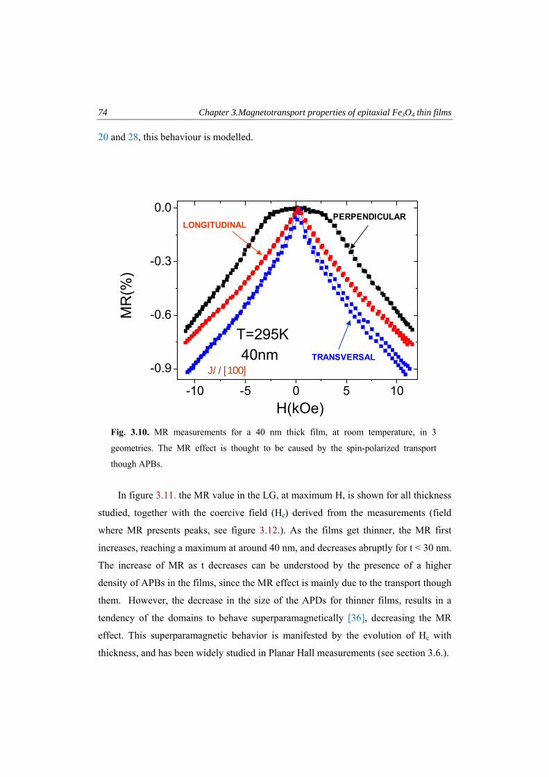
74 Chapter 3.Magnetotransport properties of epitaxial Fe3O4 thin films
20 and 28, this behaviour is modelled.
In figure 3.11. the MR value in the LG, at maximum H, is shown for all thickness
studied, together with the coercive field (Hc) derived from the measurements (field
where MR presents peaks, see figure 3.12.). As the films get thinner, the MR first
increases, reaching a maximum at around 40 nm, and decreases abruptly for t < 30 nm.
The increase of MR as t decreases can be understood by the presence of a higher
density of APBs in the films, since the MR effect is mainly due to the transport though
them. However, the decrease in the size of the APDs for thinner films, results in a
tendency of the domains to behave superparamagnetically [36], decreasing the MR
effect. This superparamagnetic behavior is manifested by the evolution of Hc with
thickness, and has been widely studied in Planar Hall measurements (see section 3.6.).
-10 -5 0 5 10
-0.9
-0.6
-0.3
0.0
40nm
MR
(%)
H(kOe)
T=295K
LONGITUDINAL
TRANSVERSAL
PERPENDICULAR
J//[100]
Fig. 3.10. MR measurements for a 40 nm thick film, at room temperature, in 3
geometries. The MR effect is thought to be caused by the spin-polarized transport
though APBs.
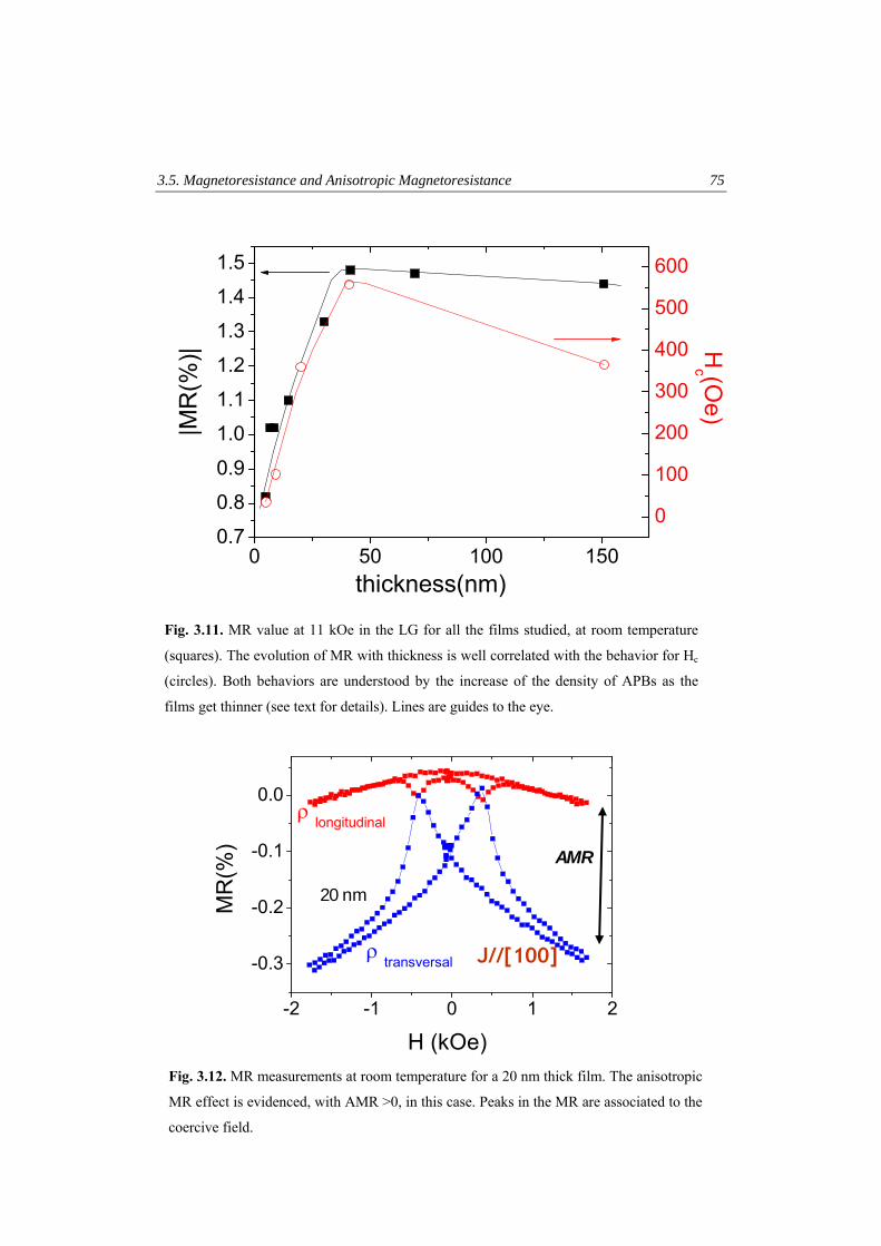
3.5. Magnetoresistance and Anisotropic Magnetoresistance 75
Fig. 3.11. MR value at 11 kOe in the LG for all the films studied, at room temperature
(squares). The evolution of MR with thickness is well correlated with the behavior for Hc
(circles). Both behaviors are understood by the increase of the density of APBs as the
films get thinner (see text for details). Lines are guides to the eye.
0
100
200
300
400
500
600
0 50 100 1500.7
0.8
0.9
1.0
1.1
1.2
1.3
1.4
1.5
|MR
(%)| H
c (Oe)
thickness(nm)
Fig. 3.12. MR measurements at room temperature for a 20 nm thick film. The anisotropic
MR effect is evidenced, with AMR >0, in this case. Peaks in the MR are associated to the
coercive field.
-2 -1 0 1 2
-0.3
-0.2
-0.1
0.0
ρ transversal
MR
(%)
H (kOe)
ρ longitudinal
J//[100]
20 nm
AMR
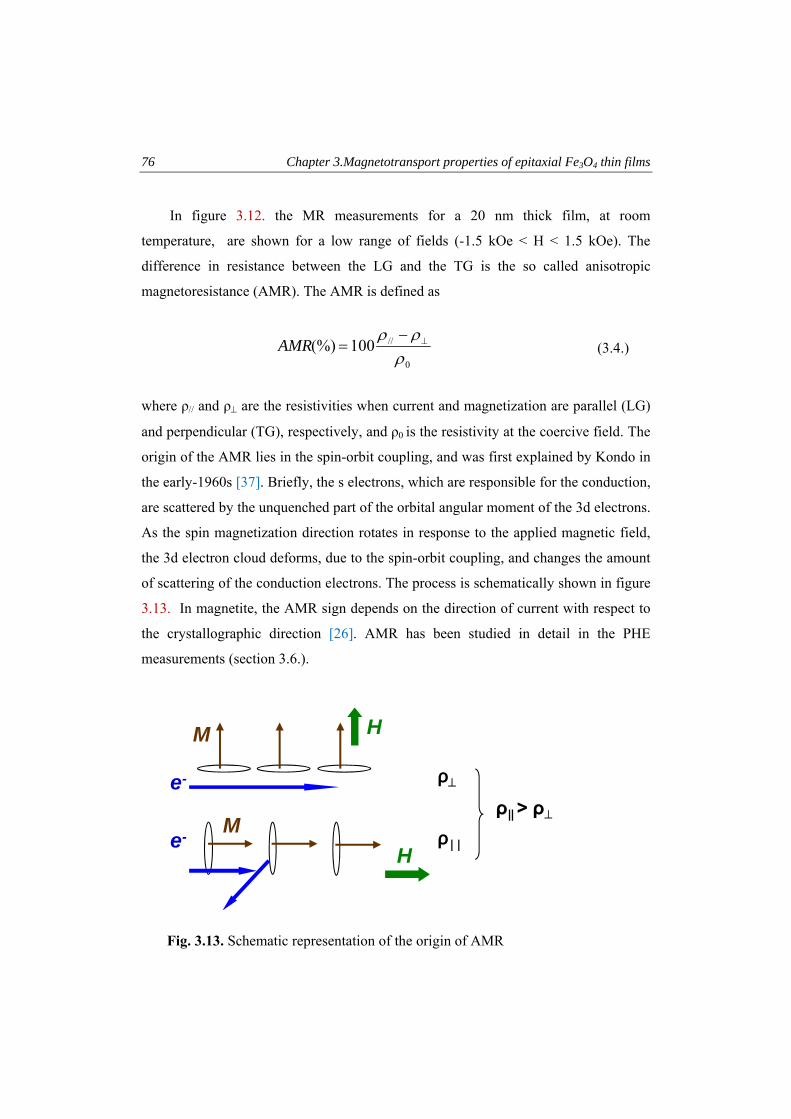
76 Chapter 3.Magnetotransport properties of epitaxial Fe3O4 thin films
In figure 3.12. the MR measurements for a 20 nm thick film, at room
temperature, are shown for a low range of fields (-1.5 kOe < H < 1.5 kOe). The
difference in resistance between the LG and the TG is the so called anisotropic
magnetoresistance (AMR). The AMR is defined as
0
//100(%)ρ
ρρ ⊥−=AMR (3.4.)
where ρ// and ρ⊥ are the resistivities when current and magnetization are parallel (LG)
and perpendicular (TG), respectively, and ρ0 is the resistivity at the coercive field. The
origin of the AMR lies in the spin-orbit coupling, and was first explained by Kondo in
the early-1960s [37]. Briefly, the s electrons, which are responsible for the conduction,
are scattered by the unquenched part of the orbital angular moment of the 3d electrons.
As the spin magnetization direction rotates in response to the applied magnetic field,
the 3d electron cloud deforms, due to the spin-orbit coupling, and changes the amount
of scattering of the conduction electrons. The process is schematically shown in figure
3.13. In magnetite, the AMR sign depends on the direction of current with respect to
the crystallographic direction [26]. AMR has been studied in detail in the PHE
measurements (section 3.6.).
Fig. 3.13. Schematic representation of the origin of AMR
H
e-
M
Hρ||
ρ⊥
ρ|| > ρ⊥
e-M
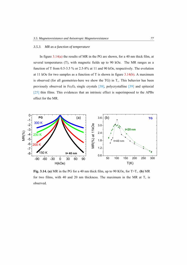
3.5. Magnetoresistance and Anisotropic Magnetoresistance 77
3.5.3. MR as a function of temperature
In figure 3.14(a) the results of MR in the PG are shown, for a 40 nm thick film, at
several temperatures (T), with magnetic fields up to 90 kOe. The MR ranges as a
function of T from 0.5-3.5 % or 2.5-8% at 11 and 90 kOe, respectively. The evolution
at 11 kOe for two samples as a function of T is shown in figure 3.14(b). A maximum
is observed (for all geometries-here we show the TG) in Tv. This behavior has been
previously observed in Fe3O4 single crystals [38], polycrystalline [39] and epitaxial
[25] thin films. This evidences that an intrinsic effect is superimposed to the APBs
effect for the MR.
Fig. 3.14. (a) MR in the PG for a 40 nm thick film, up to 90 KOe, for T>Tv. (b) MR
for two films, with 40 and 20 nm thickness. The maximum in the MR at Tv is
observed.
t= 40 nm
PG
-90 -60 -30 0 30 60 90-8-7-6-5-4-3-2-10
200 K
150 K
300 K
MR
(%)
H(kOe)
250 K
50 100 150 200 250 3000.6
1.2
1.8
2.4
3.0
3.6
MR
(%) a
t 11k
Oe
T(K)
TG
t=40 nm
t=20 nm
(a) (b)
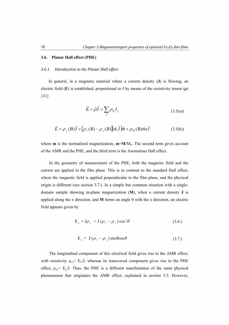
78 Chapter 3.Magnetotransport properties of epitaxial Fe3O4 thin films
3.6. Planar Hall effect (PHE)
3.6.1. Introduction to the Planar Hall effect
In general, in a magnetic material where a current density (J) is flowing, an
electric field (E) is established, proportional to J by means of the resistivity tensor (ρ)
[40]:
∑==j
jij JJE ρρrr ~ (3.5(a))
[ ]( ) JxmBmJmBBJBE H
rrrrrrr)(.)()()( // ρρρρ +−+= ⊥⊥ (3.5(b))
where m is the normalized magnetization, m=M/M0. The second term gives account
of the AMR and the PHE, and the third term is the Anomalous Hall effect.
In the geometry of measurement of the PHE, both the magnetic field and the
current are applied in the film plane. This is in contrast to the standard Hall effect,
where the magnetic field is applied perpendicular to the film plane, and the physical
origin is different (see section 3.7.). In a simple but common situation with a single-
domain sample showing in-plane magnetization (M), when a current density J is
applied along the x direction, and M forms an angle θ with the x direction, an electric
field appears given by
θρρρ 2//x cos )( J + J =E ⊥⊥ − (3.6.)
θθρρ cossin )( J =E //y ⊥− (3.7.)
The longitudinal component of this electrical field gives rise to the AMR effect,
with resistivity ρxx= Ex/J, whereas its transversal component gives rise to the PHE
effect, ρxy= Ey/J. Thus, the PHE is a different manifestation of the same physical
phenomenon that originates the AMR effect, explained in section 3.5. However,
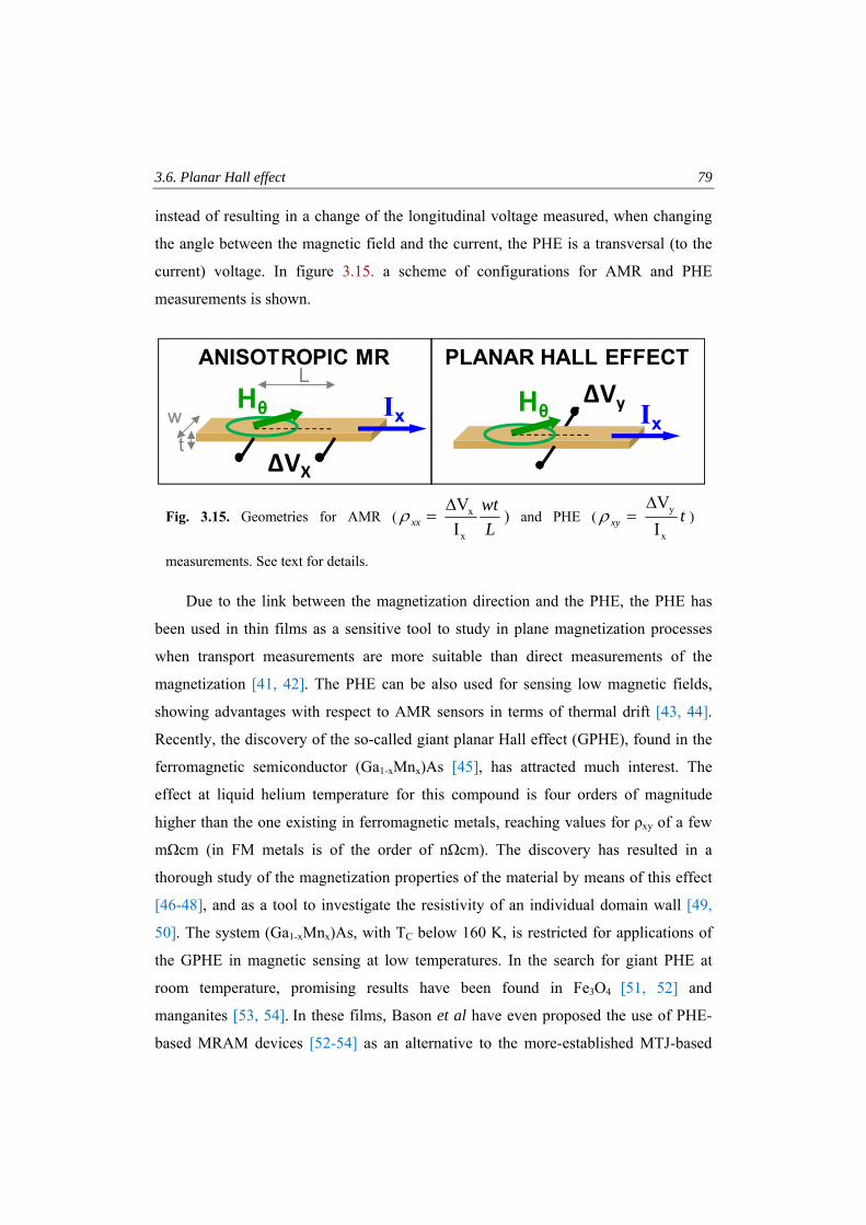
3.6. Planar Hall effect 79
instead of resulting in a change of the longitudinal voltage measured, when changing
the angle between the magnetic field and the current, the PHE is a transversal (to the
current) voltage. In figure 3.15. a scheme of configurations for AMR and PHE
measurements is shown.
Due to the link between the magnetization direction and the PHE, the PHE has
been used in thin films as a sensitive tool to study in plane magnetization processes
when transport measurements are more suitable than direct measurements of the
magnetization [41, 42]. The PHE can be also used for sensing low magnetic fields,
showing advantages with respect to AMR sensors in terms of thermal drift [43, 44].
Recently, the discovery of the so-called giant planar Hall effect (GPHE), found in the
ferromagnetic semiconductor (Ga1-xMnx)As [45], has attracted much interest. The
effect at liquid helium temperature for this compound is four orders of magnitude
higher than the one existing in ferromagnetic metals, reaching values for ρxy of a few
mΩcm (in FM metals is of the order of nΩcm). The discovery has resulted in a
thorough study of the magnetization properties of the material by means of this effect
[46-48], and as a tool to investigate the resistivity of an individual domain wall [49,
50]. The system (Ga1-xMnx)As, with TC below 160 K, is restricted for applications of
the GPHE in magnetic sensing at low temperatures. In the search for giant PHE at
room temperature, promising results have been found in Fe3O4 [51, 52] and
manganites [53, 54]. In these films, Bason et al have even proposed the use of PHE-
based MRAM devices [52-54] as an alternative to the more-established MTJ-based
Fig. 3.15. Geometries for AMR (Lwt
xxx
x
IV Δ=ρ ) and PHE ( txy
x
y
IV
Δ
=ρ )
measurements. See text for details.
IxHθ
ΔVX
IxHθ
ΔVy
PLANAR HALL EFFECTANISOTROPIC MR
tw
L
80 Chapter 3.Magnetotransport properties of epitaxial Fe3O4 thin films
technology.
3.6.2. PHE as a function of film thickness (room temperature)
At room temperature the PHE has been studied in films with thickness of 5, 9,
15, 40 and 150 nm. For the study of the PHE, all measurements were done with the
applied magnetic field forming a fixed angle with the current, θ=45º, since the signal
will be maximum in this geometry when saturation in magnetization is reached. From
equation 3.7.:
J2
J =E //)(45º)(45ºy
⊥−=
ρρρ xy (3.8.)
(For simplicity in notation, we will refer ρxy45º as ρxy from now on). From these
measurements, the AMR can be directly derived:
xx
xyAMRρρ
200(%) = (3.9.)
To confirm that the even response measured at 45º was caused by the PHE, we
also measured with a 135º configuration (ρxy135º = -ρxy
45º), see equation 3.7.). After
subtracting the common offset, signals with opposite sign were obtained (see the
particular case for the 40 nm-thick film at room temperature in the figure 3.16(a)). In
figure 3.16(b) the results of the PHE for the 40 nm-thick film with current applied in
two different directions, J//[110] and J//[100], are compared (van Der Pauw and
optically-lithographed bar, respectively). The sign is different, which indicates that the
AMR is positive (ρ//>ρ) if J//[100] whereas it is negative (ρ||<ρ) if J//[110]. Such a
difference in the sign of the AMR in Fe3O4 has been explained by Ziese and Blythe
with a phenomenological model in which the AMR is expressed as a function of the
magnetocrystalline anisotropy constants [26]. As discussed in such reference, the
AMR sign and its absolute value have an intrinsic origin related to the spin-orbit
coupling via the magnetocrystalline anisotropy constants.
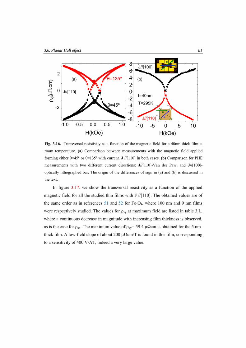
3.6. Planar Hall effect 81
In figure 3.17. we show the transversal resistivity as a function of the applied
magnetic field for all the studied thin films with J //[110]. The obtained values are of
the same order as in references 51 and 52 for Fe3O4, where 100 nm and 9 nm films
were respectively studied. The values for ρxy at maximum field are listed in table 3.I.,
where a continuous decrease in magnitude with increasing film thickness is observed,
as is the case for ρxx. The maximum value of ρxy=-59.4 µΩcm is obtained for the 5 nm-
thick film. A low-field slope of about 200 µΩcm/T is found in this film, corresponding
to a sensitivity of 400 V/AT, indeed a very large value.
Fig. 3.16. Transversal resistivity as a function of the magnetic field for a 40nm-thick film at
room temperature. (a) Comparison between measurements with the magnetic field applied
forming either θ=45º or θ=135º with current. J //[110] in both cases. (b) Comparison for PHE
measurements with two different current directions: J//[110]-Van der Paw, and J//[100]-
optically lithographed bar. The origin of the differences of sign in (a) and (b) is discussed in
the text.
J
H
-10 -5 0 5 10-8-6-4-202468
t=40nm
J//[100]
J//[110]
H(kOe)
T=295K
JH
(b)
ρ xy( μ
Ω.c
m )
-1.0 -0.5 0.0 0.5 1.0
-2
0
2
θ=45º
θ=135º
H(kOe)
J//[110]
(a)
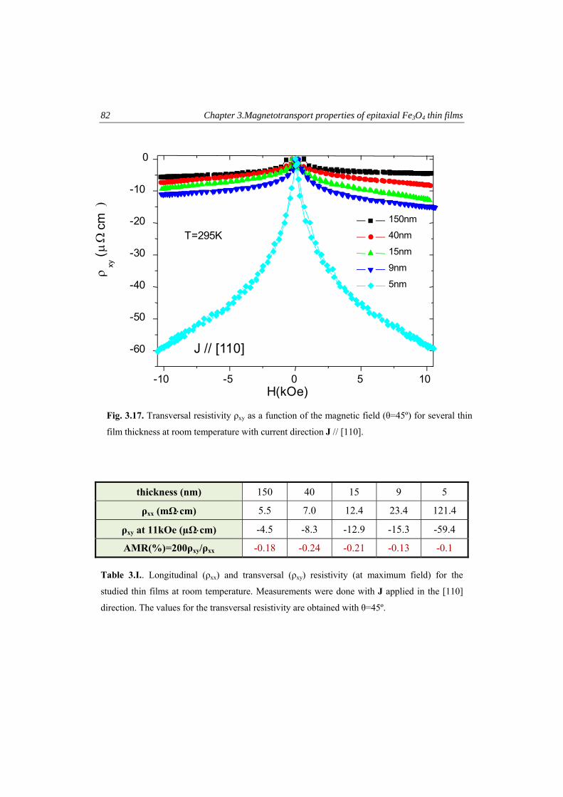
82 Chapter 3.Magnetotransport properties of epitaxial Fe3O4 thin films
thickness (nm) 150 40 15 9 5
ρxx (mΩ⋅cm) 5.5 7.0 12.4 23.4 121.4
ρxy at 11kOe (µΩ⋅cm) -4.5 -8.3 -12.9 -15.3 -59.4
AMR(%)=200ρxy/ρxx -0.18 -0.24 -0.21 -0.13 -0.1
Table 3.I.. Longitudinal (ρxx) and transversal (ρxy) resistivity (at maximum field) for the
studied thin films at room temperature. Measurements were done with J applied in the [110]
direction. The values for the transversal resistivity are obtained with θ=45º.
-10 -5 0 5 10
-60
-50
-40
-30
-20
-10
0
T=295K150nm
40nm
15nm
9nm
5nm
ρxy
(μΩ
cm)
H(kOe)
J // [110]
Fig. 3.17. Transversal resistivity ρxy as a function of the magnetic field (θ=45º) for several thin
film thickness at room temperature with current direction J // [110].
3.6. Planar Hall effect 83
An important issue to point out is the evolution of the films towards
superparamagnetic (SP) behaviour as the films decrease in thickness, due to the
reduction of the ferrimagnetic exchange coupling existing between spins surrounding
the APBs [36]. As explained before, the density of APBs varies as t-1/2 [20, 21]. The
APDs for ultrathin films have sizes of a few unit cells, and their magnetic moments
start to fluctuate due to the thermal energy. The progressive shift towards zero field
found for the peaks associated with the coercive field in our PHE measurements, as
well as the increase of the slope for ρxy at high fields suggest the occurrence of this
phenomenon. These features influence the possible applications of the PHE observed
in these films. The SP tendency is also reflected when the AMR is calculated from
PHE measurements (see table 3.I). The AMR has an approximately constant value of -
0.2% for films above 10 nm, in agreement with bulk results and thin films in this
range of thickness for J//[110] (ref. 26). Below 10 nm, an important decrease in
magnitude occurs, compatible with the absence of anisotropy found for SP samples
[36]. This behavior is the same as MR measurements shown in section 3.5.2. Thus, for
very thin films (below 5 nm), the PHE will be limited in magnitude by the difficulty in
magnetizing the sample and the decrease in the AMR value. Therefore, thinner films
than the studied here are not expected to present higher PHE values than the reported
ones. It should be also noticed the difficulty to use the GPHE in very thin Fe3O4 films
for magnetic storage since an improvement in signal magnitude with decreasing
thickness also implies a decrease in coercive field. On the other hand, the
superparamagnetic tendency implies a less-hysteretical GPHE effect, which is
welcomed for magnetic sensing.
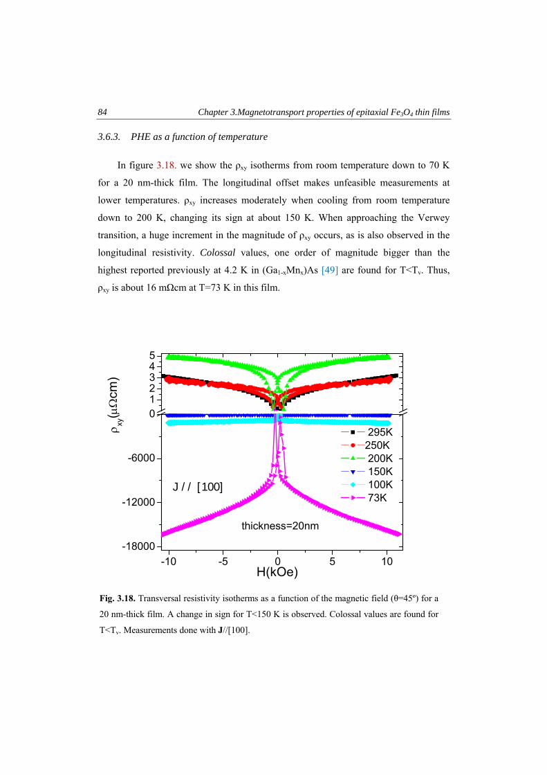
84 Chapter 3.Magnetotransport properties of epitaxial Fe3O4 thin films
3.6.3. PHE as a function of temperature
In figure 3.18. we show the ρxy isotherms from room temperature down to 70 K
for a 20 nm-thick film. The longitudinal offset makes unfeasible measurements at
lower temperatures. ρxy increases moderately when cooling from room temperature
down to 200 K, changing its sign at about 150 K. When approaching the Verwey
transition, a huge increment in the magnitude of ρxy occurs, as is also observed in the
longitudinal resistivity. Colossal values, one order of magnitude bigger than the
highest reported previously at 4.2 K in (Ga1-xMnx)As [49] are found for T<Tv. Thus,
ρxy is about 16 mΩcm at T=73 K in this film.
-10 -5 0 5 10-18000
-12000
-6000
012345
295K250K 200K 150K 100K 73K
thickness=20nm
ρ xy(μ
Ωcm
)
H(kOe)
J // [100]
Fig. 3.18. Transversal resistivity isotherms as a function of the magnetic field (θ=45º) for a
20 nm-thick film. A change in sign for T<150 K is observed. Colossal values are found for
T<Tv. Measurements done with J//[100].
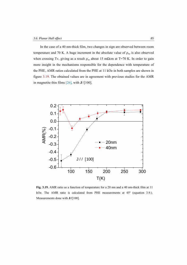
3.6. Planar Hall effect 85
In the case of a 40 nm-thick film, two changes in sign are observed between room
temperature and 70 K. A huge increment in the absolute value of ρxy is also observed
when crossing Tv, giving as a result ρxy about 15 mΩcm at T=70 K. In order to gain
more insight in the mechanisms responsible for the dependence with temperature of
the PHE, AMR ratios calculated from the PHE at 11 kOe in both samples are shown in
figure 3.19. The obtained values are in agreement with previous studies for the AMR
in magnetite thin films [26], with J//[100].
100 150 200 250 300-0.6
-0.5
-0.4
-0.3
-0.2
-0.1
0.0
0.1
0.2
AMR
(%)
T(K)
20nm 40nm
J // [100]
Fig. 3.19. AMR ratio as a function of temperature for a 20 nm and a 40 nm-thick film at 11
kOe. The AMR ratio is calculated from PHE measurements at 45º (equation 3.9.).
Measurements done with J//[100].
86 Chapter 3.Magnetotransport properties of epitaxial Fe3O4 thin films
For both films, AMR≈0.2%, independent of temperature, is found for
temperatures above 150 K. Different tendencies are followed in each thin film below
this temperature. Whereas in the case of the 20 nm-thick film, a change in sign occurs,
giving as a result negative values for T<150K, for the 40 nm film ρxy is positive except
in the surroundings of Tv. The changes of sign in the AMR are likely related to
intrinsic changes in the magnetocristalline anisotropy in this temperature range as
previously observed in bulk single crystals [55]. Such changes will dramatically
modify the anisotropy constants, which correspondingly will vary the AMR/PHE
value as demonstrated in the phenomenological model presented in ref. 26. The
magnetic anisotropy in these films is expected to depend strongly on the film
thickness and detailed magnetic studies beyond the scope of the present study would
be required to clarify the quantitative relationship between the magnetic anisotropy
changes and the AMR/PHE.
One important result inferred from the obtained AMR temperature dependence is
that the absolute value of the AMR is large below the Verwey transition. The ground
state of Fe3O4 below the Verwey transition is still a matter of debate [56]. Recent
experiments indicate that pure electrostatic models do not seem to be able to explain
the ground state below the Verwey transition and the electron-lattice coupling must
play a key role in order to stabilize it [56]. The large values of the AMR below the
Verwey transition observed by us give evidence for a substantial magnetocrystalline
anisotropy of the ground state caused by a significant spin-orbital coupling. This
suggests that the claimed strong electron-lattice coupling could arise from a large spin-
orbital coupling.
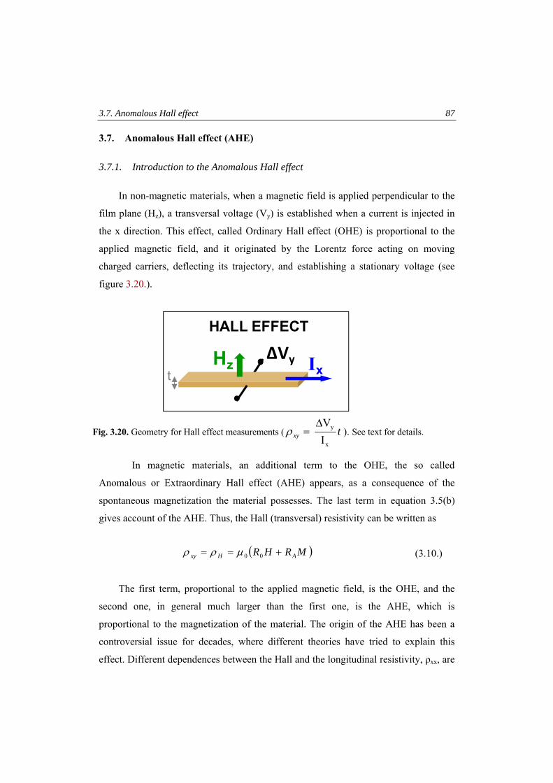
3.7. Anomalous Hall effect 87
3.7. Anomalous Hall effect (AHE)
3.7.1. Introduction to the Anomalous Hall effect
In non-magnetic materials, when a magnetic field is applied perpendicular to the
film plane (Hz), a transversal voltage (Vy) is established when a current is injected in
the x direction. This effect, called Ordinary Hall effect (OHE) is proportional to the
applied magnetic field, and it originated by the Lorentz force acting on moving
charged carriers, deflecting its trajectory, and establishing a stationary voltage (see
figure 3.20.).
In magnetic materials, an additional term to the OHE, the so called
Anomalous or Extraordinary Hall effect (AHE) appears, as a consequence of the
spontaneous magnetization the material possesses. The last term in equation 3.5(b)
gives account of the AHE. Thus, the Hall (transversal) resistivity can be written as
( )MRHR AHxy +== 00μρρ (3.10.)
The first term, proportional to the applied magnetic field, is the OHE, and the
second one, in general much larger than the first one, is the AHE, which is
proportional to the magnetization of the material. The origin of the AHE has been a
controversial issue for decades, where different theories have tried to explain this
effect. Different dependences between the Hall and the longitudinal resistivity, ρxx, are
Fig. 3.20. Geometry for Hall effect measurements ( txyx
y
IV
Δ
=ρ ). See text for details.
IxHz
ΔVy
HALL EFFECT
t
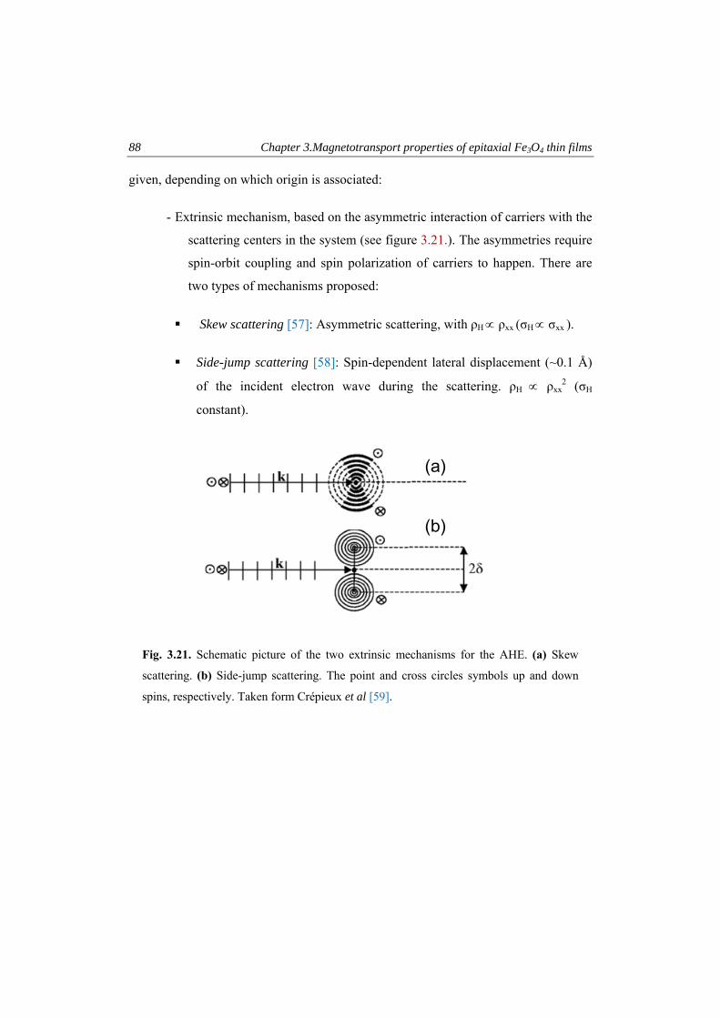
88 Chapter 3.Magnetotransport properties of epitaxial Fe3O4 thin films
given, depending on which origin is associated:
- Extrinsic mechanism, based on the asymmetric interaction of carriers with the
scattering centers in the system (see figure 3.21.). The asymmetries require
spin-orbit coupling and spin polarization of carriers to happen. There are
two types of mechanisms proposed:
Skew scattering [57]: Asymmetric scattering, with ρH ∝ ρxx (σH ∝ σxx ).
Side-jump scattering [58]: Spin-dependent lateral displacement (~0.1 Å)
of the incident electron wave during the scattering. ρH ∝ ρxx2 (σH
constant).
(b)
(a)
Fig. 3.21. Schematic picture of the two extrinsic mechanisms for the AHE. (a) Skew
scattering. (b) Side-jump scattering. The point and cross circles symbols up and down
spins, respectively. Taken form Crépieux et al [59].
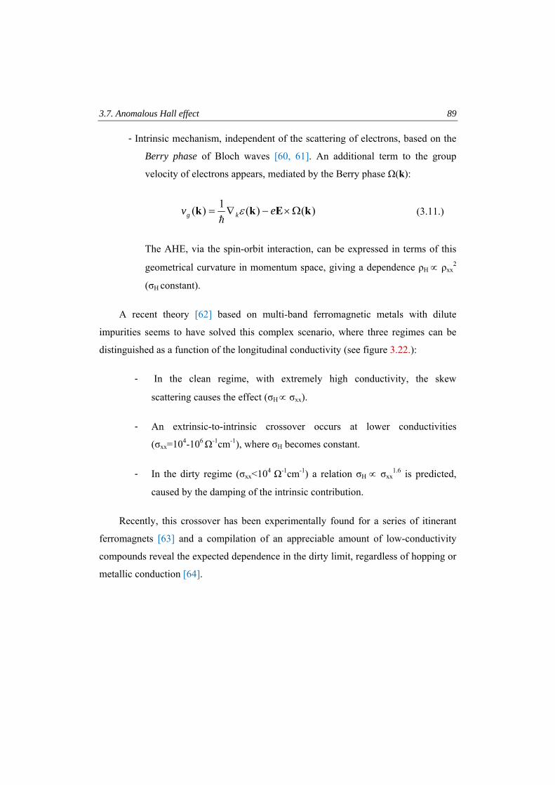
3.7. Anomalous Hall effect 89
- Intrinsic mechanism, independent of the scattering of electrons, based on the
Berry phase of Bloch waves [60, 61]. An additional term to the group
velocity of electrons appears, mediated by the Berry phase Ω(k):
)()(1)( kEkk Ω×−∇= ev kg εh
(3.11.)
The AHE, via the spin-orbit interaction, can be expressed in terms of this
geometrical curvature in momentum space, giving a dependence ρH ∝ ρxx2
(σH constant).
A recent theory [62] based on multi-band ferromagnetic metals with dilute
impurities seems to have solved this complex scenario, where three regimes can be
distinguished as a function of the longitudinal conductivity (see figure 3.22.):
- In the clean regime, with extremely high conductivity, the skew
scattering causes the effect (σH ∝ σxx).
- An extrinsic-to-intrinsic crossover occurs at lower conductivities
(σxx=104-106 Ω-1cm-1), where σH becomes constant.
- In the dirty regime (σxx<104 Ω-1cm-1) a relation σH ∝ σxx1.6 is predicted,
caused by the damping of the intrinsic contribution.
Recently, this crossover has been experimentally found for a series of itinerant
ferromagnets [63] and a compilation of an appreciable amount of low-conductivity
compounds reveal the expected dependence in the dirty limit, regardless of hopping or
metallic conduction [64].
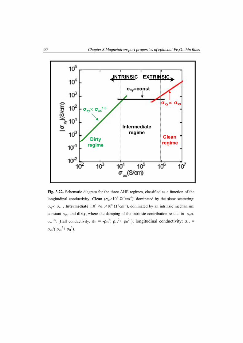
90 Chapter 3.Magnetotransport properties of epitaxial Fe3O4 thin films
Fig. 3.22. Schematic diagram for the three AHE regimes, classified as a function of the
longitudinal conductivity: Clean (σxx>106 Ω-1cm-1), dominated by the skew scattering:
σxy∝ σxx , Intermediate (104 <σxx<106 Ω-1cm-1), dominated by an intrinsic mechanism:
constant σxy, and dirty, where the damping of the intrinsic contribution results in σxy∝
σxx1.6. [Hall conductivity: σH = -ρH/( ρxx
2+ ρH2 ); longitudinal conductivity: σxx =
ρxx/( ρxx2+ ρH
2).
Cleanregime
Dirtyregime
Intermediateregime
σxy∝ σxx1.6
σxy=const
σxy ∝ σxx
EXTRINSICINTRINSIC
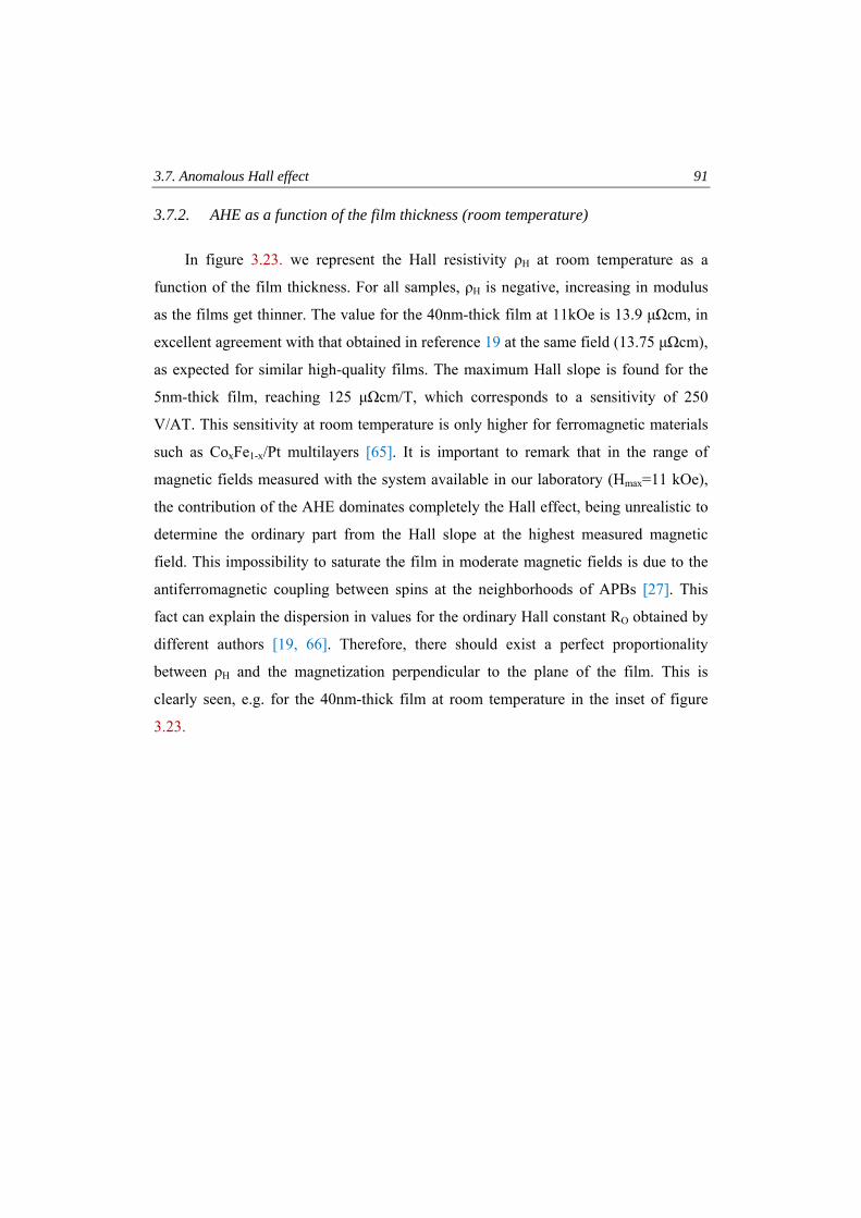
3.7. Anomalous Hall effect 91
3.7.2. AHE as a function of the film thickness (room temperature)
In figure 3.23. we represent the Hall resistivity ρH at room temperature as a
function of the film thickness. For all samples, ρH is negative, increasing in modulus
as the films get thinner. The value for the 40nm-thick film at 11kOe is 13.9 μΩcm, in
excellent agreement with that obtained in reference 19 at the same field (13.75 μΩcm),
as expected for similar high-quality films. The maximum Hall slope is found for the
5nm-thick film, reaching 125 μΩcm/T, which corresponds to a sensitivity of 250
V/AT. This sensitivity at room temperature is only higher for ferromagnetic materials
such as CoxFe1-x/Pt multilayers [65]. It is important to remark that in the range of
magnetic fields measured with the system available in our laboratory (Hmax=11 kOe),
the contribution of the AHE dominates completely the Hall effect, being unrealistic to
determine the ordinary part from the Hall slope at the highest measured magnetic
field. This impossibility to saturate the film in moderate magnetic fields is due to the
antiferromagnetic coupling between spins at the neighborhoods of APBs [27]. This
fact can explain the dispersion in values for the ordinary Hall constant RO obtained by
different authors [19, 66]. Therefore, there should exist a perfect proportionality
between ρH and the magnetization perpendicular to the plane of the film. This is
clearly seen, e.g. for the 40nm-thick film at room temperature in the inset of figure
3.23.
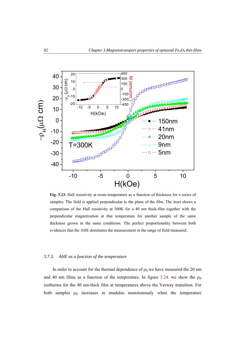
92 Chapter 3.Magnetotransport properties of epitaxial Fe3O4 thin films
3.7.3. AHE as a function of the temperature
In order to account for the thermal dependence of ρH we have measured the 20 nm
and 40 nm films as a function of the temperature. In figure 3.24. we show the ρH
isotherms for the 40 nm-thick film at temperatures above the Verwey transition. For
both samples ρH increases in modulus monotonously when the temperature
-10 -5 0 5 10
-40
-30
-20
-10
0
10
20
30
40
150nm 41nm 20nm 9nm 5nm
−ρH(μ
Ω c
m)
H(kOe)
T=300K
-10 -5 0 5 10-20
-10
0
10
20
-450-300-1500150300450 M
(emu/cm
3)−ρH
(μΩ
cm
)
H(kOe)
Fig. 3.23. Hall resistivity at room temperature as a function of thickness for a series of
samples. The field is applied perpendicular to the plane of the film. The inset shows a
comparison of the Hall resistivity at 300K for a 40 nm thick-film together with the
perpendicular magnetization at that temperature for another sample of the same
thickness grown in the same conditions. The perfect proportionality between both
evidences that the AHE dominates the measurement in the range of field measured.
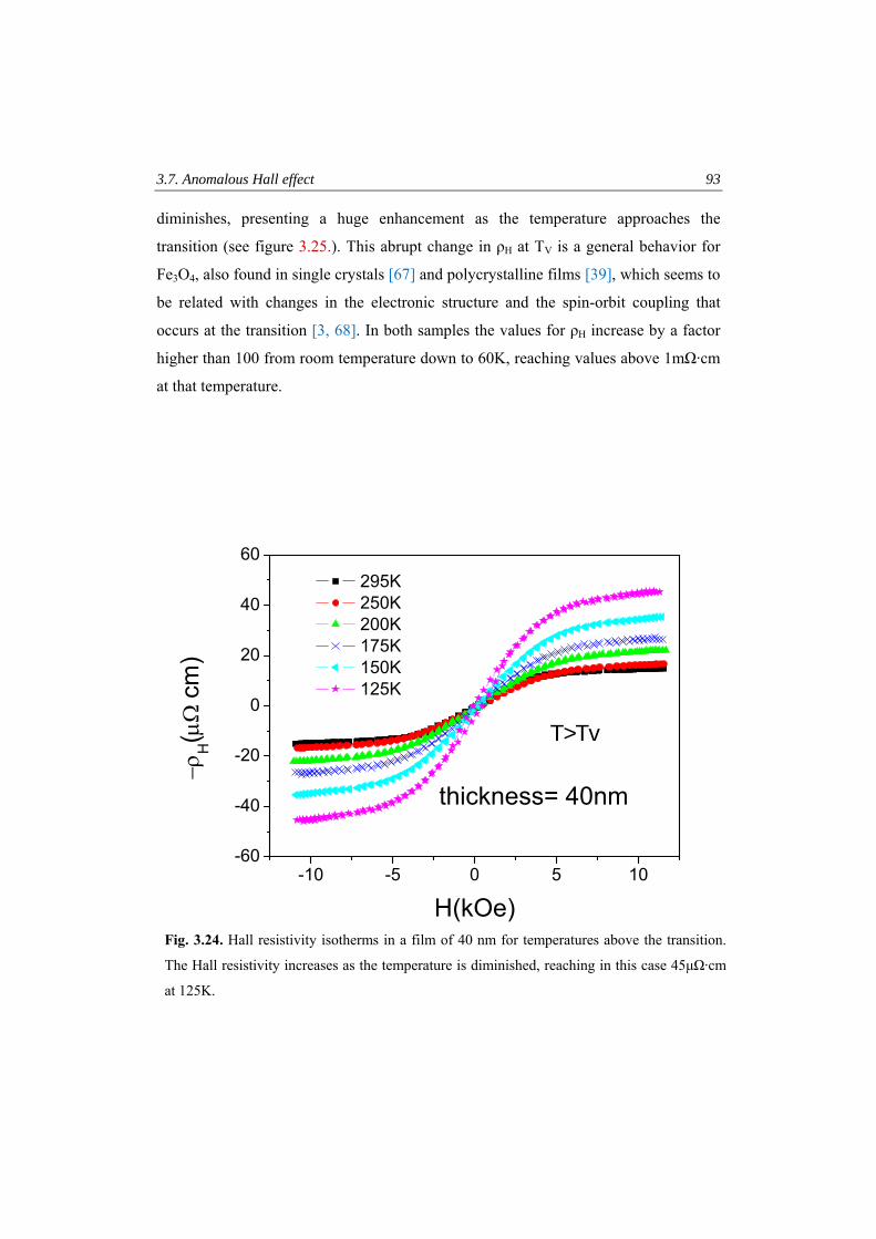
3.7. Anomalous Hall effect 93
diminishes, presenting a huge enhancement as the temperature approaches the
transition (see figure 3.25.). This abrupt change in ρH at TV is a general behavior for
Fe3O4, also found in single crystals [67] and polycrystalline films [39], which seems to
be related with changes in the electronic structure and the spin-orbit coupling that
occurs at the transition [3, 68]. In both samples the values for ρH increase by a factor
higher than 100 from room temperature down to 60K, reaching values above 1mΩ·cm
at that temperature.
-10 -5 0 5 10-60
-40
-20
0
20
40
60
−ρH(μ
Ω c
m)
H(kOe)
295K 250K 200K 175K 150K 125K
thickness= 40nm
T>Tv
Fig. 3.24. Hall resistivity isotherms in a film of 40 nm for temperatures above the transition.
The Hall resistivity increases as the temperature is diminished, reaching in this case 45μΩ·cm
at 125K.
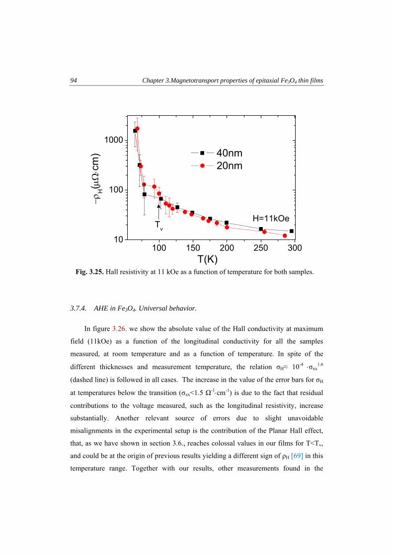
94 Chapter 3.Magnetotransport properties of epitaxial Fe3O4 thin films
3.7.4. AHE in Fe3O4. Universal behavior.
In figure 3.26. we show the absolute value of the Hall conductivity at maximum
field (11kOe) as a function of the longitudinal conductivity for all the samples
measured, at room temperature and as a function of temperature. In spite of the
different thicknesses and measurement temperature, the relation σH≈ 10-4 ⋅σxx1.6
(dashed line) is followed in all cases. The increase in the value of the error bars for σH
at temperatures below the transition (σxx<1.5 Ω-1⋅cm-1) is due to the fact that residual
contributions to the voltage measured, such as the longitudinal resistivity, increase
substantially. Another relevant source of errors due to slight unavoidable
misalignments in the experimental setup is the contribution of the Planar Hall effect,
that, as we have shown in section 3.6., reaches colossal values in our films for T<Tv,
and could be at the origin of previous results yielding a different sign of ρH [69] in this
temperature range. Together with our results, other measurements found in the
100 150 200 250 30010
100
1000
40nm 20nm
−ρH(μ
Ω⋅c
m)
T(K)
H=11kOeTv
Fig. 3.25. Hall resistivity at 11 kOe as a function of temperature for both samples.
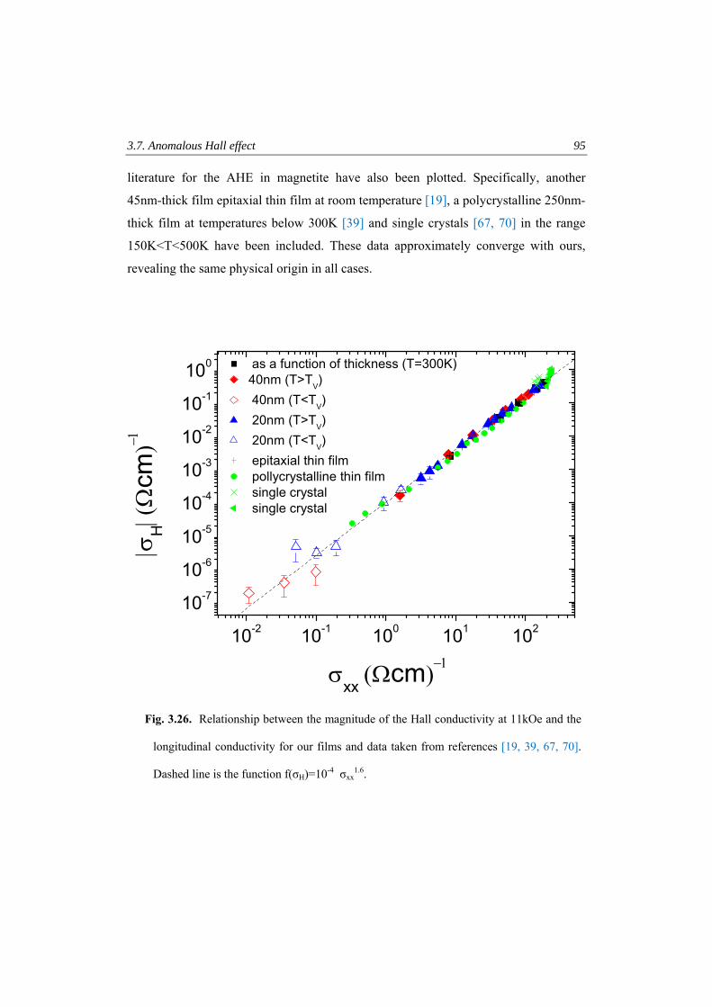
3.7. Anomalous Hall effect 95
literature for the AHE in magnetite have also been plotted. Specifically, another
45nm-thick film epitaxial thin film at room temperature [19], a polycrystalline 250nm-
thick film at temperatures below 300K [39] and single crystals [67, 70] in the range
150K<T<500K have been included. These data approximately converge with ours,
revealing the same physical origin in all cases.
10-2 10-1 100 101 102
10-7
10-6
10-5
10-4
10-3
10-2
10-1
100
as a function of thickness (T=300K)40nm (T>TV) 40nm (T<TV) 20nm (T>TV) 20nm (T<TV) epitaxial thin film pollycrystalline thin film single crystal single crystal
σxx (Ωcm)−1
|σH| (
Ωcm
)−1
Fig. 3.26. Relationship between the magnitude of the Hall conductivity at 11kOe and the
longitudinal conductivity for our films and data taken from references [19, 39, 67, 70].
Dashed line is the function f(σH)=10-4 σxx1.6.
96 Chapter 3.Magnetotransport properties of epitaxial Fe3O4 thin films
We explained in section 3.1.3 some effects appearing in epitaxial Fe3O4 thin
films, associated with the presence of APBs. These effects become more evident the
thinner the films are. In previous sections we have shown how the APBs influence the
magnetotransport properties measured: resistivity, MR and PHE. However, in this
section, we have shown that the AHE in Fe3O4 thin films presents a universal
behavior. First, the enhancement in the Hall resistivity as the temperature is
diminished seems to be related with the increase in the longitudinal resistance, as a
consequence of the broadening that occurs in the band gap as TV is approached. This
results in huge Hall resistivities of the order of mΩ·cm at low temperatures. Second,
the dependence σH ∝ σxx1.6 found over four decades of longitudinal conductivity is in
accordance with the recent unifying theory for the AHE presented in section 3.7.1.
[62]. This relation is followed by samples in a wide range of thicknesses and
irrespective of the measurement temperature. Furthermore, the same dependence for
σH is found in other samples of magnetite taken from the literature, regardless they are
single crystals or polycrystalline thin films. The theory [62] explains that the
magnitude of the AHE is determined by the degree of resonance caused by the
location of Fermi level around an anticrossing of band dispersions. Besides, it assumes
metallic conduction. From our results we can infer that the Verwey transition,
associated with a cubic-to-monoclinic structure transition, does not play an important
role in this behavior. It was pointed out before that this dependence is also followed in
hopping conduction [64]. In the case of Fe3O4, our results suggest that this dependence
also takes place irrespective of the different conduction mechanisms occurring above
and below TV [3]. Other important issue is related with the presence of APBs. As was
mentioned before, some magnitudes such as the resistivity or magnetization are
subjected to important changes from the bulk material to the thin films, due to the
presence of these structural defects. The moderate magnetoresistance ratios in films
are explained by the spin-polarized transport through them. However, the AHE is
again not affected by the density of APBs, which decreases with film thickness.
Finally, it should also be remarked that the presence of stress in epitaxial thin films
caused by the substrate could eventually have an influence in the band structure in
comparison with the bulk material, but the convergence of all data reveals that this is
3.7. Anomalous Hall effect 97
not an important issue for the AHE. All these facts support the belief that the relation
σH ∝ σxx1.6 is universal for this low-conductivity regime.
3.7.5. Fe3O4 inside the AHE dirty regime of conductivities.
Finally, for completeness, we show in figure 3.27. a wide compilation of results
for the AHE found in the literature for magnetic compounds, together with those for
Fe3O4 previously shown in figure 3.26., all of them in the dirty regime of conduction.
We include data for metals, oxides, and magnetically-doped semiconductors, with
completely different crystallographic structure, magnetic density when doping, and
electrical conduction. The Hall conductivity follows the universal relationship σH ∝
σxx1.6 over six decades of longitudinal conductivity in all cases. The different
proportionality constants in the fits are explained in theory to be caused by a different
impurity potential [62]. The universal scaling is followed in spite of the big
differences between these compounds. The theory developed in reference 62 was done
for metallic conduction, with the band playing a vital role in this effect, so it is
surprising the good convergence of all these results.
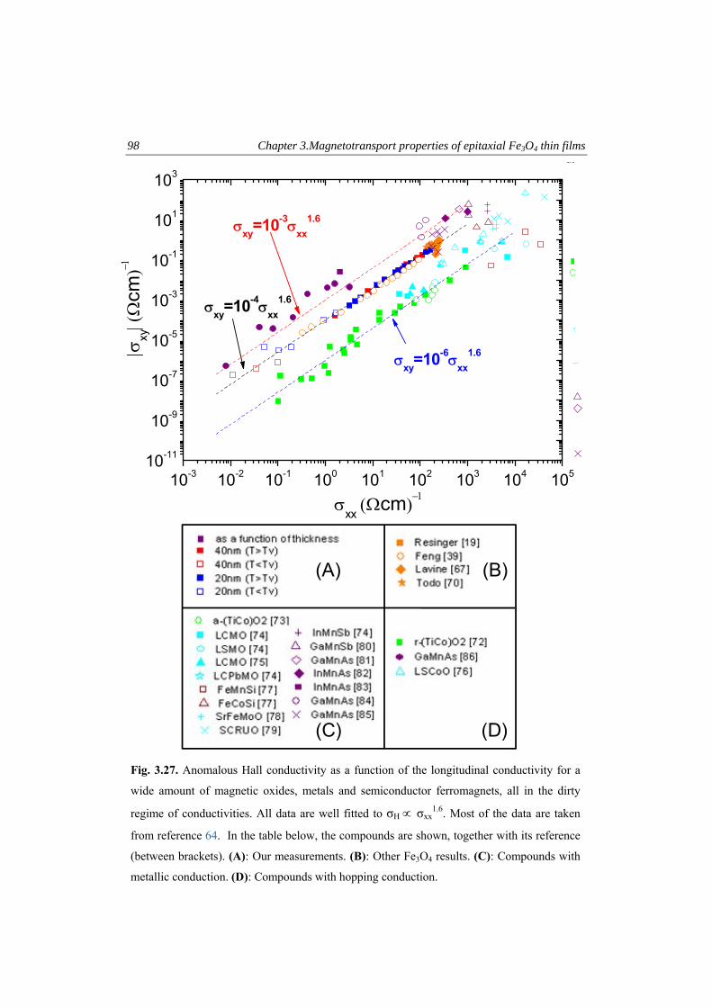
98 Chapter 3.Magnetotransport properties of epitaxial Fe3O4 thin films
10-3 10-2 10-1 100 101 102 103 104 10510-11
10-9
10-7
10-5
10-3
10-1
101
103
σxy=10-6σxx1.6
σxy=10-4σxx1.6
as
σxx (Ωcm)−1
|σxy
| (Ω
cm)−1
σxy=10-3σxx1.6
(A) (B)
(C) (D)
Fig. 3.27. Anomalous Hall conductivity as a function of the longitudinal conductivity for a
wide amount of magnetic oxides, metals and semiconductor ferromagnets, all in the dirty
regime of conductivities. All data are well fitted to σH ∝ σxx1.6. Most of the data are taken
from reference 64. In the table below, the compounds are shown, together with its reference
(between brackets). (A): Our measurements. (B): Other Fe3O4 results. (C): Compounds with
metallic conduction. (D): Compounds with hopping conduction.
3.8. Conclusions 99
3.8. Conclusions
We have grown high-quality epitaxial Fe3O4 films on MgO substrates and studied
systematically their magnetotransport properties. A complete optical lithography
process was successfully performed for the films, allowing technically difficult
measurements, below the Verwey transition.
Resistivity measurements show a perfect agreement with previous results of other
groups. ρ follows the relation t-1/2, as a consequence of the increase of the APBs when
film thickness decreases. Measurements as a function of temperature show a decrease
of Tv as films get thinner, together with a smoothing of the Verwey transition,
becoming undistinguishable for t<10 nm.
Magnetoresistance measurements reproduce previous results in the literature, and
can be understood by the spin-polarized transport through APBs. The tendency
towards the superparamagnetic behavior of the APDs is evidenced for ultra-thin films.
An intrinsic peak for the absolute value of the MR at Tv indicates that an intrinsic
phenomenon is superimposed to the extrinsic effect caused by APBs.
Thickness and temperature dependences of the giant planar Hall effect in the
films have been studied. Samples with moderately-high APBs density show higher
PHE signals due to the induced increase in the absolute value of the resistivity
anisotropy, making them interesting candidates for magnetic sensing and non-volatile
memories, as well as for magnetization studies through transport measurements. A
record value of the planar Hall effect at room temperature of |ρxy|≈60 µΩcm was
obtained for the 5 nm-thick film. As a function of temperature, the PHE increases in
magnitude, reaching colossal values below the Verwey transition, in the range of a few
mΩcm. The anisotropic magnetoresistance values inferred from these measurements
indicate that the ground state below the Verwey transition likely bears a substantial
spin-orbit coupling.
Anomalous Hall effect measurements in the films show that the dependence σH ∝
σxx1.6 is fulfilled over four decades of longitudinal conductivity, irrespective of

100 Chapter 3.Magnetotransport properties of epitaxial Fe3O4 thin films
thickness or measurement temperature. Comparison with literature confirms this
behavior is general for this compound, as well as for others in the same (low) regime
of conduction. This result supports a recent theory developed to explain the anomalous
Hall effect, indicating the universality of this relation in the dirty regime of
conductivities.
Chapter 4
Conduction in atomic-sized
magnetic metallic constrictions
created by FIB
This chapter reports the study of electron conduction in metallic constrictions, with
sizes in the atomic range. First, a novel technique for the fabrication of
nanoconstrictions at room temperature in metallic materials will be presented, based
on the potentialities that the dual-beam equipment offers.
We will show that it is possible to create atomic-sized constrictions inside the vacuum
chamber where the sample is fabricated. Second, this method has been used for
experiments in a magnetic metal as iron, where phenomena such as ballistic
magnetoresistance and ballistic anisotropic magnetoresistance have been investigated.
102 Chapter 4. Exploring conduction in atomic-size magnetic constrictions created by FIB
4.1. Theoretical background for atomic-sized constrictions
4.1.1. Introduction
In the macroscopic world, the nature of the electrical conduction in metals does
not depend of its size. However, when this size approaches the atomic regime,
electrons can be conducted without being scattered, and Ohm’s Law is not fulfilled
anymore. In this regime, called ballistic, the normal concept for conduction is
changed, being necessary to invoke the wave nature of the electrons in the conductor
for a proper description. The energy scales involved are so large than quantum effects
are visible at room temperature [1].
The creation of constrictions with these dimensions is a hard task, and laboratory
techniques which manipulate in the molecular and atomic scale are necessary,
normally under highly strict environmental conditions
4.1.2. Conduction regimes for metals
Let us imagine two big metallic electrodes, connected by a constriction (also
denoted as contact) of length L, through which electrons flow.
If this contact has macroscopic dimensions, the electrons are scattered when
passing, since L > l (where l is the elastic mean free path, typically a few tens of
nanometers in metals at low temperatures). In this case, Ohm’s law is fulfilled, and the
conductance of this constriction is given by the classical expression:
σS/LG = (4.1.)
where σ is the conductivity of the material, and S is the section of the contact. We call
this regime of conduction diffusive.
When the dimensions of a contact are much smaller than l the electrons will pass
through it without being scattered. This regime is called ballistic. In such contacts
there will be a large potential gradient near the contact, causing the electrons to
4.1. Theoretical background for atomic-sized constrictions 103
accelerate within a short distance. This problem was first treated semiclassically by
Sharvin [2], obtaining for the conductance: 2
F
2
λπa
h2eG ⎟⎟
⎠
⎞⎜⎜⎝
⎛= (4.2.)
where a is the radius of the contact. In this case, the resistance is not proportional, as it
was the case in the diffusive regime, to the number of scattering events. The resistance
of the ballistic channel tends to zero, and it is the boundaries between the leads and
channel which are responsible of the resistance of the system. In Sharvin’s formula, G
depends on the electronic density through the Fermi wavelength λF, and it is
independent of σ and l. Quantum mechanics are only introduced in this treatment by
Fermi Statistics.
This semiclassical approach is, however, not valid, when the contacts are atomic-
sized, with a few atoms contributing to the conduction of electrons. In this case L ~ λF
(from a few to fractions of Å) and we enter into the full quantum limit. This problem
was treated by Landauer [3], reaching for the value of the conductance:
∑=
=N
ii
1
2
h2eG τ (4.3.)
where τi is the transmission coefficient of the channel i. The conductance is
proportional to the value
h2eG
2
0 = (4.4.)
which is called the “quantum of conductance”, and whose corresponding resistance
value, the quantum of resistance, is R0=12.9 kΩ. Thus, the wave nature of electrons is
manifested by the quantization of the conductance. This result is analogous to the
propagation of waves through wave guides, when the channel width is of the order of
the incident wavelength.
The existence of conduction channels is related to the presence of wavefunctions
at the Fermi energy. For the simplest 1D case, the number of conduction channels
104 Chapter 4. Exploring conduction in atomic-size magnetic constrictions created by FIB
results from the number of intersecting branches of a 1D dispersion curve with the
Fermi energy. For metallic systems, the occurrence of single channel conduction is
thus expected in monovalent metals. Moreover, realistic geometries for atomic-size
contacts can deviate significantly from a periodic 1D system, resulting in non-perfect
transmission factors. It has indeed been shown theoretically and experimentally that
perfect single-channel conduction is rather rare, exclusively limited to monovalent
metals like Au [4]. The full atomic orbital overlap and bonding has to be considered in
describing realistic atomic-sized contacts. When doing so, it appears that the number
of conducting channels is roughly of the order of the number of valence electrons.
Transmission factors can also depend sensitively on the exact geometry of the contact
and the orbitals considered. Hence, it should be underlined that conductance
quantization in an integer number of G0 is only obtained for idealized 1D systems. In
fact, it can be shown that transmission factors vary continuously with orbital overlap:
if it were possible to continuously change the interatomic distance between two central
atoms of an atomic chain, the conductance would smoothly decrease. Thus, it is likely
that conductance steps that are experimentally observed when creating atomic contacts
are associated with the stability of some specific atomic configurations rather than a
signature of quantized transport [1].
4.1.3. Typical methods for the fabrication of atomic contacts
As it was commented in the introductory part, the methods for creating atomic
contacts are mainly laboratory techniques, normally working at Helium liquid
temperature, and in ultra-high vacuum conditions. These experiments have led to huge
advances in the understanding of electron conduction in atomic-sized metal structures.
Between the most commonly used we should cite:
(i) Mechanical break junctions (MBJ) [5]: A metallic film is broken in a
controllable way, by bending a flexible substrate on which the material
has previously been deposited. This is clearly the most documented
method for fabricating atomic contacts.
4.1. Theoretical background for atomic-sized constrictions 105
(ii) Use of STM [6]: The tip is contacted to a surface, and the distance
between the tip-sample distance is varied at a constant low bias voltage
(~10 mV), recording the current.
(iii) Electrical Break Junctions [7]: Atoms are electromigrated by the
appliance of large current densities on a previously (usually by EBL)
patterned neck of a metallic thin film.
(iv) Electrochemical junctions [8]: In an electrochemical bath, a previously
patterned (EBL) gap is filled by electrodeposition.
106 Chapter 4. Exploring conduction in atomic-size magnetic constrictions created by FIB
4.2. Atomic constrictions in magnetic materials
4.2.1. Introduction
Due to the spin degeneracy of the conduction electrons in magnetic materials, the
quantum of conductance includes a factor of two. Due to the strong exchange energy,
magnetic materials have their band structure split. Conducting channels are therefore
spin dependent and the conductance quantum in magnetic materials is
heG
2
0 =M (4.5.)
Hence, in the case of single-channel conduction, electronic transport would be
fully polarized and the material would become (locally) a half-metallic conductor.
4.2.2. Ballistic magnetoresistance (BMR)
Since the conduction in metals in the ballistic regime is governed by the band
structure, the magnetoresistance properties of magnetic materials should therefore be
affected, due to the absence of spin-dependent diffusion. In the case of GMR, this fact
was studied theoretically by Schep et al [9], although experimental results in this issue
were unsuccessful [10].
The topic was revived with spectacular results, when MR values of a few hundred
per cent were measured in Ni contacts formed by approaching wires mechanically
[11]. These results were also obtained in nanocontacts of other ferromagnetic
materials by using different techniques, by several groups [12-16]. The effect
proposed, coined as Ballistic Magnetoresistance (BMR), was associated to the
presence or non-presence of a domain wall in the contact, blocking or letting the
electrons pass through the contact. When the magnetizations in the electrodes are
parallel, the conductance is of the order of the conductance quantum, but in the
antiparallel case, electrons are partially reflected because the majority spin channel
changes its spin direction in the contact. Hence, magnetoresistance would be expected
to reach extremely large values when the sample resistance is of the order of 10 kΩ.
4.2. Atomic constrictions in magnetic materials 107
These results supposed a high impact in the Spintronics community, since new
devices based on this effect, higher than GMR, could be performed. However, next
experiments [17-19] trying to reproduce previous results revealed that actually
mechanical artifacts, such as atomic reconfigurations or magnetostriction (change of
volume in a magnetic material when its magnetization changes), were responsible for
this high effect, and actually BMR would be only of the order of a few tens per cent
[20]. The high controversial scenario lived in these years had its maximum point in
2004, in the “Symposium on the Controversy Over Ballistic Magnetoresistance’ at the
Ninth Intermag Conference (Anaheim, CA, January 5–9, 2004)”. Currently, the
scientific community has basically concluded that the impressive BMR is a
consequence of spurious effects [20], although it should be also remarked that it is still
unclear if magnetic nanocontacts of high transmission factors can be made [1]. This
would require making a 1D wire, without imperfections, with a diameter smoothly
increasing when connected to the diffusive reservoirs.
4.2.3. Ballistic anisotropic magnetoresistance (BAMR)
Another different finding in atomic-sized contacts was a large anisotropy in the
MR of the contacts, whose magnitude and angular dependence were found to be very
distinct from bulk materials, the so called ballistic anisotropic magnetoresistance
(BAMR).
Anisotropic magnetoresistance in bulk ferromagnetic materials (diffusive regime)
was introduced in chapter 3. In a few words, in a FM it is possible to describe its
conductance in two separated channels, for spin up and down directions [21]. When
adding to the energy of the system the spin-orbit coupling (L-S), the wavefunctions of
electrons have to be recalculated, not being anymore eigenstates of Sz, since the L-S
mixes spin states. This mixing is anisotropic, giving as a consequence an anisotropy of
the resistance [22, 23]:
108 Chapter 4. Exploring conduction in atomic-size magnetic constrictions created by FIB
0
//100(%)Aρρρ ⊥−
=MR (4.6.)
The sign of the AMR depends on the band structure of the FM, normally being
positive in metals (ρ// > ρ).
The dependence of the AMR with the angle θ formed by the current and the
magnetization is:
( ) θρρρθρ 2// cos)( ⊥⊥ −=− (4.6.)
In ballistic transport, the AMR has to be recalculated, since the structural,
electronic and magnetic properties of atoms change. For instance, the quenching of the
orbital moment will not be as quenched as in bulk [24], and the spin-orbit coupling
will increase substantially [20]. Theoretical studies of BAMR in chains of Ni and Co
[25, 26] indicate that the effect would be much higher than in bulk, of the order of G0,
and with an angle dependence much more abrupt.
Some experimental measurements support these theories. Specifically, we can
cite the work by Sokolov et al [27], where in Co contacts made by electrodeposition,
changes in the AMR of the order of the quantum of conductance were found, and the
work by Viret et al [28], where iron contacts fabricated by mechanical break junction
were systematically studied, finding even higher effects for samples in the tunneling
regime than in the metallic (ballistic) regime. However, critical voices have claimed
that atomic reconfigurations in the contact, rather than an intrinsic electronic effect,
are the most feasible reason for this behavior [29].
4.2.4. Objective of this work
After having exposed the interesting effects appearing in magnetic atomic-sized
constrictions, together with the polemics associated to these high-impact results, it
seems crucial the creation of magnetic nanocontacts free from spurious effects, to
4.2. Atomic constrictions in magnetic materials 109
clearly discriminate whether these effects are intrinsic, or not, in magnetic materials.
The typical techniques used for this purpose (see section 4.1.3.) control extraordinarily
well the reduction of the contacts to the atomic regime. However, the constrictions
fabricated by these methods are not tightly attached to a substrate, favoring the
mechanical artifacts to be present. Besides, the realization of real devices using BMR
or BAMR with those methods is not possible, due to its incompatibility for
integration. Therefore, nanolithography techniques have been used aiming to create
stable nanoconstrictions at room temperature, which could lead to immense
applications. However, the resolution of techniques such as EBL or FIB makes really
challenging the creation of contacts smaller than 100 nm. Some results can be cited
using these techniques [30-35], but MR effects found are, in general, similar to those
for bulk, and the lack of reproducibility is evident.
Thus, the work presented in this chapter has had as objective the creation of
magnetic nanoconstrictions in the ballistic regime of conduction by means of FIB,
trying to systematically study the BMR and BAMR. The work has been successful in
the realization of an approach that creates atomic-sized contacts, although the study of
MR effects in magnetic nanoconstrictions has, on the contrary, been less satisfactory.
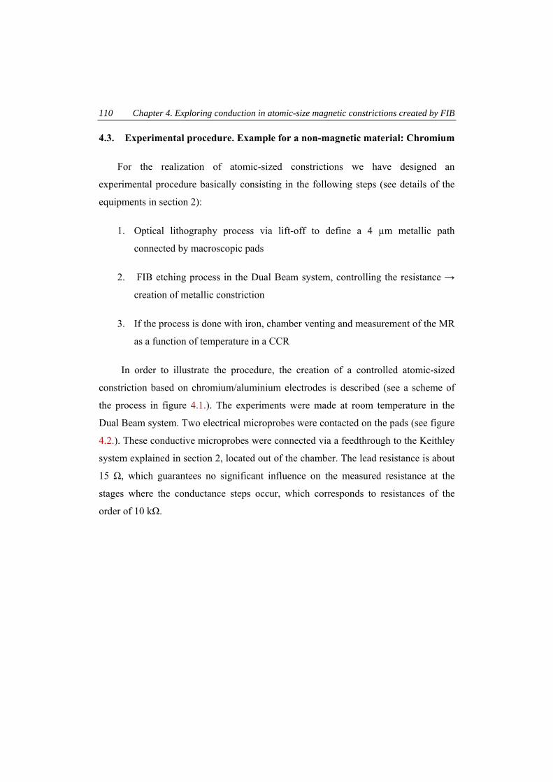
110 Chapter 4. Exploring conduction in atomic-size magnetic constrictions created by FIB
4.3. Experimental procedure. Example for a non-magnetic material: Chromium
For the realization of atomic-sized constrictions we have designed an
experimental procedure basically consisting in the following steps (see details of the
equipments in section 2):
1. Optical lithography process via lift-off to define a 4 µm metallic path
connected by macroscopic pads
2. FIB etching process in the Dual Beam system, controlling the resistance →
creation of metallic constriction
3. If the process is done with iron, chamber venting and measurement of the MR
as a function of temperature in a CCR
In order to illustrate the procedure, the creation of a controlled atomic-sized
constriction based on chromium/aluminium electrodes is described (see a scheme of
the process in figure 4.1.). The experiments were made at room temperature in the
Dual Beam system. Two electrical microprobes were contacted on the pads (see figure
4.2.). These conductive microprobes were connected via a feedthrough to the Keithley
system explained in section 2, located out of the chamber. The lead resistance is about
15 Ω, which guarantees no significant influence on the measured resistance at the
stages where the conductance steps occur, which corresponds to resistances of the
order of 10 kΩ.
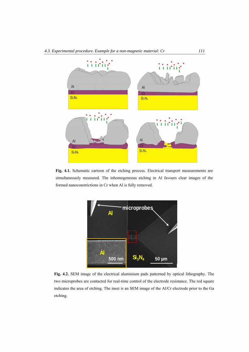
4.3. Experimental procedure. Example for a non-magnetic material: Cr 111
Fig. 4.2. SEM image of the electrical aluminium pads patterned by optical lithography. The
two microprobes are contacted for real-time control of the electrode resistance. The red square
indicates the area of etching. The inset is an SEM image of the Al/Cr electrode prior to the Ga
etching.
Al
Al
microprobes
500 nm 50 µmSi3N4
Fig. 4.1. Schematic cartoon of the etching process. Electrical transport measurements are
simultaneously measured. The inhomogeneous etching in Al favours clear images of the
formed nanoconstrictions in Cr when Al is fully removed.
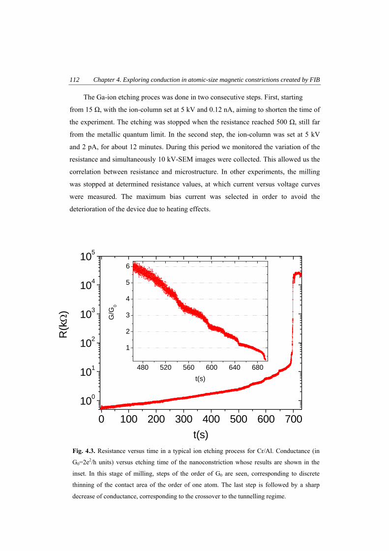
112 Chapter 4. Exploring conduction in atomic-size magnetic constrictions created by FIB
The Ga-ion etching proces was done in two consecutive steps. First, starting
from 15 Ω, with the ion-column set at 5 kV and 0.12 nA, aiming to shorten the time of
the experiment. The etching was stopped when the resistance reached 500 Ω, still far
from the metallic quantum limit. In the second step, the ion-column was set at 5 kV
and 2 pA, for about 12 minutes. During this period we monitored the variation of the
resistance and simultaneously 10 kV-SEM images were collected. This allowed us the
correlation between resistance and microstructure. In other experiments, the milling
was stopped at determined resistance values, at which current versus voltage curves
were measured. The maximum bias current was selected in order to avoid the
deterioration of the device due to heating effects.
0 100 200 300 400 500 600 700
100
101
102
103
104
105
R(kΩ
)
t(s)
480 520 560 600 640 680
1
2
3
4
5
6
G/G
0
t(s)
Fig. 4.3. Resistance versus time in a typical ion etching process for Cr/Al. Conductance (in
G0=2e2/h units) versus etching time of the nanoconstriction whose results are shown in the
inset. In this stage of milling, steps of the order of G0 are seen, corresponding to discrete
thinning of the contact area of the order of one atom. The last step is followed by a sharp
decrease of conductance, corresponding to the crossover to the tunnelling regime.
4.3. Experimental procedure. Example for a non-magnetic material: Cr 113
In figure 4.3. we show a typical resistance-versus-etching time result at a starting
value of 500 Ω. The resistance increases continuously for about 10 minutes, up to a
point, in which a 3 orders of magnitude jump is seen. Just before this abrupt change,
the resistance shows a discrete number of steps. We can see in the inset that, for this
particular case, plateaus with a small negative slope for the conductance are roughly
located near integer multiples of G0. This step-wise structure is a clear indication of the
formation of point contacts in the metal electrode before the complete breaking of the
formed nanowires. This is similar to what it is seen in experiments done with the other
techniques explained in section 4.1.3. [1]. The long experimental time to create one of
these constrictions (hundreds of seconds) compared to other techniques such as STM
or MBJ (tens of microseconds) does not favor the building of histograms with enough
statistics to assign the observed step-wise behavior to conductance quantization. From
tens of experiments, we can conclude the reproducible existence of steps in the
conductance in the verge of the metal-tunneling crossover and certain dispersion in the
specific values of the conductance plateaus, which we always observe below 4 G0.
Anyhow, previous studies indicate that conductance histograms are more irregular in
transition metals nanoconstrictions [1, 36] than in the case of monovalent metals like
Au [4]. This is due to the fact that the number of conducting channels in a single-atom
contact is determined by the number of valence electrons and its orbital state.
Theoretical works show that the conductance in non-monovalent metals strongly
depends on the specific atomic configurations of the constriction [37-39], which
suggests that strong dispersion in the specific values of the conductance plateaus are
expected in a reduced number of experiments. To determine the values where steps in
conductance occur, numerical differentiation of the G(t) curve was done. Peaks with
approximately zero maximum value are observed where plateaus in G occur. In the
particular case of figure 4.3., the fit of these peaks to a Gaussian curve gives the
maximum at the values (1.02 ± 0.01) G0, (1.72 ± 0.01) G0, (2.17 ± 0.01) G0, and (3.24
± 0.02) G0. The broadness of the found steps is a typical feature of room temperature
measurements [1, 36, 40].
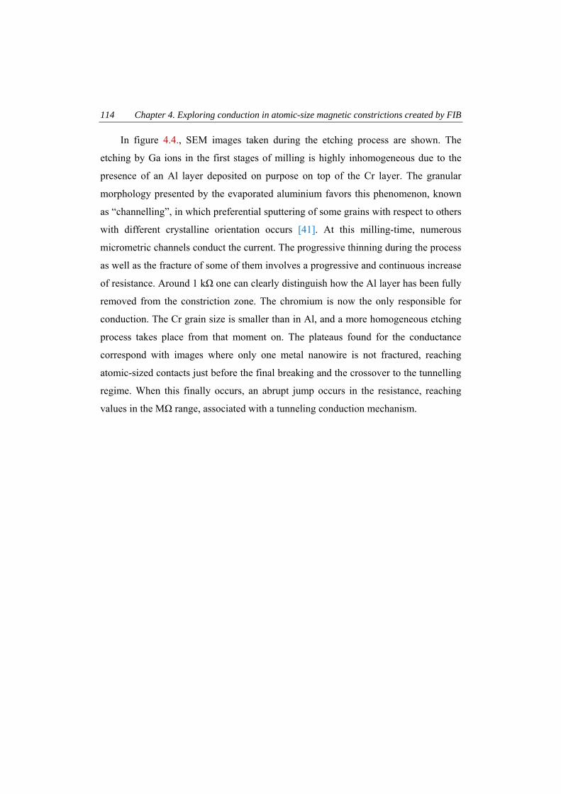
114 Chapter 4. Exploring conduction in atomic-size magnetic constrictions created by FIB
In figure 4.4., SEM images taken during the etching process are shown. The
etching by Ga ions in the first stages of milling is highly inhomogeneous due to the
presence of an Al layer deposited on purpose on top of the Cr layer. The granular
morphology presented by the evaporated aluminium favors this phenomenon, known
as “channelling”, in which preferential sputtering of some grains with respect to others
with different crystalline orientation occurs [41]. At this milling-time, numerous
micrometric channels conduct the current. The progressive thinning during the process
as well as the fracture of some of them involves a progressive and continuous increase
of resistance. Around 1 kΩ one can clearly distinguish how the Al layer has been fully
removed from the constriction zone. The chromium is now the only responsible for
conduction. The Cr grain size is smaller than in Al, and a more homogeneous etching
process takes place from that moment on. The plateaus found for the conductance
correspond with images where only one metal nanowire is not fractured, reaching
atomic-sized contacts just before the final breaking and the crossover to the tunnelling
regime. When this finally occurs, an abrupt jump occurs in the resistance, reaching
values in the MΩ range, associated with a tunneling conduction mechanism.
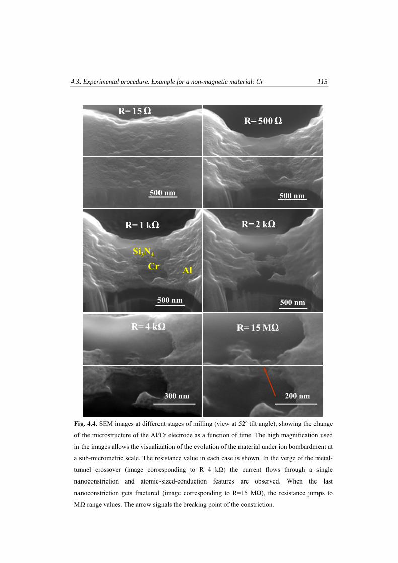
4.3. Experimental procedure. Example for a non-magnetic material: Cr 115
Fig. 4.4. SEM images at different stages of milling (view at 52º tilt angle), showing the change
of the microstructure of the Al/Cr electrode as a function of time. The high magnification used
in the images allows the visualization of the evolution of the material under ion bombardment at
a sub-micrometric scale. The resistance value in each case is shown. In the verge of the metal-
tunnel crossover (image corresponding to R=4 kΩ) the current flows through a single
nanoconstriction and atomic-sized-conduction features are observed. When the last
nanoconstriction gets fractured (image corresponding to R=15 MΩ), the resistance jumps to
MΩ range values. The arrow signals the breaking point of the constriction.
500 nm
R= 15 Ω
200 nm
R= 15 MΩR= 4 kΩ
300 nm
500 nm
R= 500 Ω
R= 1 kΩ
Si3N4
AlCr
500 nm
R= 2 kΩ
500 nm
116 Chapter 4. Exploring conduction in atomic-size magnetic constrictions created by FIB
In some constrictions, the etching was stopped at different moments, measuring
I-V curves. As it can be seen in figure 4.5., the linear I-V behavior indicates metallic
conduction, and consequently that the constriction is not broken. Once the constriction
breaks, a non-linear I-V behaviour is found, as expected in tunnelling conduction.
Fitting the I-V curves for tunnelling conduction to the Simmons model for a
rectangular tunnel barrier [42] gives as a result a barrier height of the order of 4.5 V, a
junction effective area of 300 nm2 and a barrier width of the order of 0.65 nm. The
found barrier height corresponds with the work function for chromium [43] and the
other parameters seem reasonable, evidencing the adequacy of the fit in spite of the
simplified assumptions of the model. Even though re-sputtering of some Al atoms
towards the contact area could be possible, the value found for the barrier height in the
tunneling regime seems to indicate that the electronic transport through the
nanocontact is governed by the Cr atoms.
We have not observed degradation during the measurement time (tens of seconds)
since the substrate under the formed metal constriction guarantees a robust and stable
structure. We have found that when the constriction shows resistance values of the
order of the conductance quantum, a limiting maximum power of 0.3 nW is required
to avoid degradation, which constrains the maximum applied voltage to values below
~6 mV. Considering a contact area of 0.3x0.3 nm2, a 5.5x10⁷ A/cm2 current density is
obtained, which is around three orders of magnitude larger than the maximum current
bearable by a macroscopic metallic wire. This huge current density is understood in
terms of ballistic transport through the contact [1].
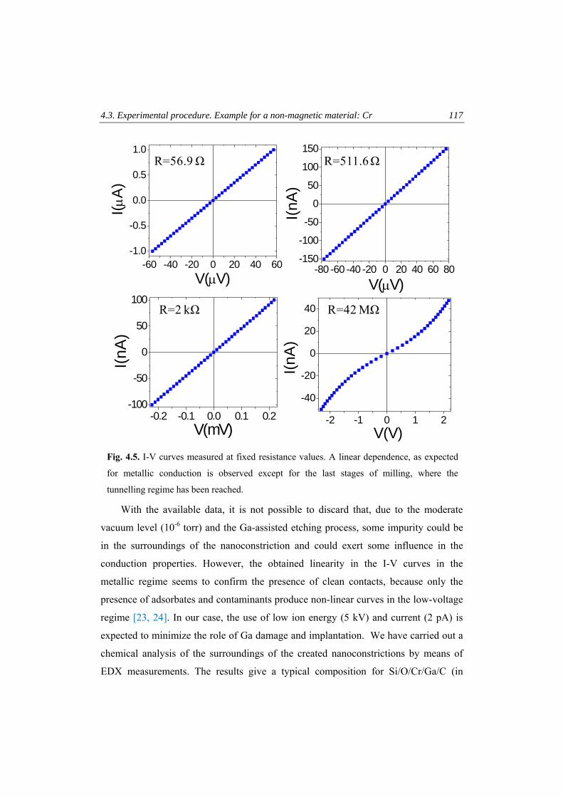
4.3. Experimental procedure. Example for a non-magnetic material: Cr 117
With the available data, it is not possible to discard that, due to the moderate
vacuum level (10-6 torr) and the Ga-assisted etching process, some impurity could be
in the surroundings of the nanoconstriction and could exert some influence in the
conduction properties. However, the obtained linearity in the I-V curves in the
metallic regime seems to confirm the presence of clean contacts, because only the
presence of adsorbates and contaminants produce non-linear curves in the low-voltage
regime [23, 24]. In our case, the use of low ion energy (5 kV) and current (2 pA) is
expected to minimize the role of Ga damage and implantation. We have carried out a
chemical analysis of the surroundings of the created nanoconstrictions by means of
EDX measurements. The results give a typical composition for Si/O/Cr/Ga/C (in
-60 -40 -20 0 20 40 60-1.0
-0.5
0.0
0.5
1.0
I(μ
A)
V(μV)
-2 -1 0 1 2
-40
-20
0
20
40
V(V)
I(nA
)-80 -60 -40 -20 0 20 40 60 80
-150
-100
-50
0
50
100
150
I(n
A)
V(μV)
-0.2 -0.1 0.0 0.1 0.2-100
-50
0
50
100
I(n
A)
V(mV)
R=56.9 Ω
R=2 kΩ
R=511.6 Ω
R=42 MΩ
Fig. 4.5. I-V curves measured at fixed resistance values. A linear dependence, as expected
for metallic conduction is observed except for the last stages of milling, where the
tunnelling regime has been reached.
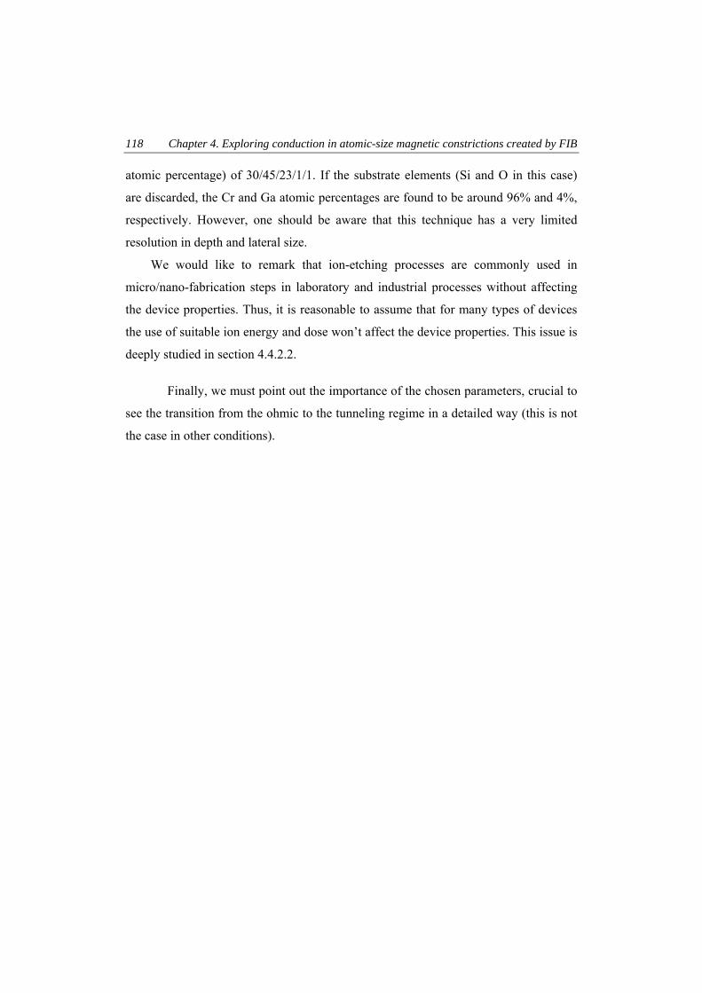
118 Chapter 4. Exploring conduction in atomic-size magnetic constrictions created by FIB
atomic percentage) of 30/45/23/1/1. If the substrate elements (Si and O in this case)
are discarded, the Cr and Ga atomic percentages are found to be around 96% and 4%,
respectively. However, one should be aware that this technique has a very limited
resolution in depth and lateral size.
We would like to remark that ion-etching processes are commonly used in
micro/nano-fabrication steps in laboratory and industrial processes without affecting
the device properties. Thus, it is reasonable to assume that for many types of devices
the use of suitable ion energy and dose won’t affect the device properties. This issue is
deeply studied in section 4.4.2.2.
Finally, we must point out the importance of the chosen parameters, crucial to
see the transition from the ohmic to the tunneling regime in a detailed way (this is not
the case in other conditions).
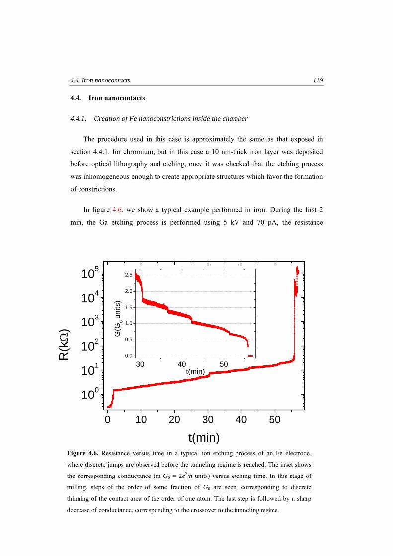
4.4. Iron nanocontacts 119
4.4. Iron nanocontacts
4.4.1. Creation of Fe nanoconstrictions inside the chamber
The procedure used in this case is approximately the same as that exposed in
section 4.4.1. for chromium, but in this case a 10 nm-thick iron layer was deposited
before optical lithography and etching, once it was checked that the etching process
was inhomogeneous enough to create appropriate structures which favor the formation
of constrictions.
In figure 4.6. we show a typical example performed in iron. During the first 2
min, the Ga etching process is performed using 5 kV and 70 pA, the resistance
0 10 20 30 40 50
100
101
102
103
104
105
R(kΩ
)
t(min)
30 40 500.0
0.5
1.0
1.5
2.0
2.5
G(G
0 uni
ts)
t(min)
Figure 4.6. Resistance versus time in a typical ion etching process of an Fe electrode,
where discrete jumps are observed before the tunneling regime is reached. The inset shows
the corresponding conductance (in G0 = 2e2/h units) versus etching time. In this stage of
milling, steps of the order of some fraction of G0 are seen, corresponding to discrete
thinning of the contact area of the order of one atom. The last step is followed by a sharp
decrease of conductance, corresponding to the crossover to the tunneling regime.
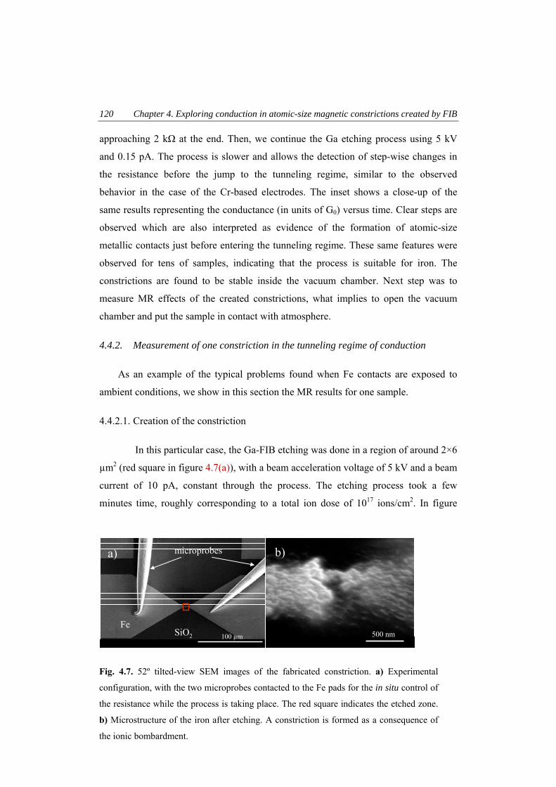
120 Chapter 4. Exploring conduction in atomic-size magnetic constrictions created by FIB
approaching 2 kΩ at the end. Then, we continue the Ga etching process using 5 kV
and 0.15 pA. The process is slower and allows the detection of step-wise changes in
the resistance before the jump to the tunneling regime, similar to the observed
behavior in the case of the Cr-based electrodes. The inset shows a close-up of the
same results representing the conductance (in units of G0) versus time. Clear steps are
observed which are also interpreted as evidence of the formation of atomic-size
metallic contacts just before entering the tunneling regime. These same features were
observed for tens of samples, indicating that the process is suitable for iron. The
constrictions are found to be stable inside the vacuum chamber. Next step was to
measure MR effects of the created constrictions, what implies to open the vacuum
chamber and put the sample in contact with atmosphere.
4.4.2. Measurement of one constriction in the tunneling regime of conduction
As an example of the typical problems found when Fe contacts are exposed to
ambient conditions, we show in this section the MR results for one sample.
4.4.2.1. Creation of the constriction
In this particular case, the Ga-FIB etching was done in a region of around 2×6
µm2 (red square in figure 4.7(a)), with a beam acceleration voltage of 5 kV and a beam
current of 10 pA, constant through the process. The etching process took a few
minutes time, roughly corresponding to a total ion dose of 1017 ions/cm2. In figure
100 µm100 µm 500 nm500 nmSiO2
Fe
microprobesa) b)
100 µm100 µm 500 nm500 nm100 µm100 µm 500 nm500 nmSiO2
Fe
microprobesa) b)
Fig. 4.7. 52º tilted-view SEM images of the fabricated constriction. a) Experimental
configuration, with the two microprobes contacted to the Fe pads for the in situ control of
the resistance while the process is taking place. The red square indicates the etched zone.
b) Microstructure of the iron after etching. A constriction is formed as a consequence of
the ionic bombardment.
4.4. Iron nanocontacts 121
4.7(b) the microstructure of the constriction after the milling is shown.
In figure 4.8. we show the evolution of the resistance with the process time.
Since the initial resistance of the iron electrode is Ri ~3 kΩ, the resistance
corresponding to the etched part (Rc) is the measured value minus Ri (R=Ri + Rc).
After 2 minutes of etching, R starts to increase abruptly, and the FIB column is
stopped when Rc ≈ 8 kΩ. The R is measured during several minutes, finding that the
constriction, in the metallic regime, is stable under the high vacuum conditions of the
chamber (P~10-6 mbar). To avoid the possible deterioration when exposed to ambient
conditions, a ~10 nm-thick layer of Pt-C was deposited by electrons (FEBID) on top
of the etched zone (one single deposition, at 0º), using (CH3)3Pt(CpCH3) as gas
precursor. The high resistance of this material, because of the high amount of carbon,
guarantees a resistance in parallel to the constriction of the order of tens of MΩ [44],
which is confirmed by the negligible change of R while the deposit is done.
Figure 4.8. Resistance of the iron electrode as a function of the process time. The FIB
etching is stopped when the resistance reaches 11 kΩ (Rc~8 kΩ). The constriction is covered
by a thin layer of Pt-C, deposited by FEBID. The fabricated nanostructure is stable inside
the vacuum chamber.
0 2 4 6 8
4
6
8
10
end depos. Pt-C
start depos. Pt-C
endetching
R (k
Ω)
t (min)
startetching
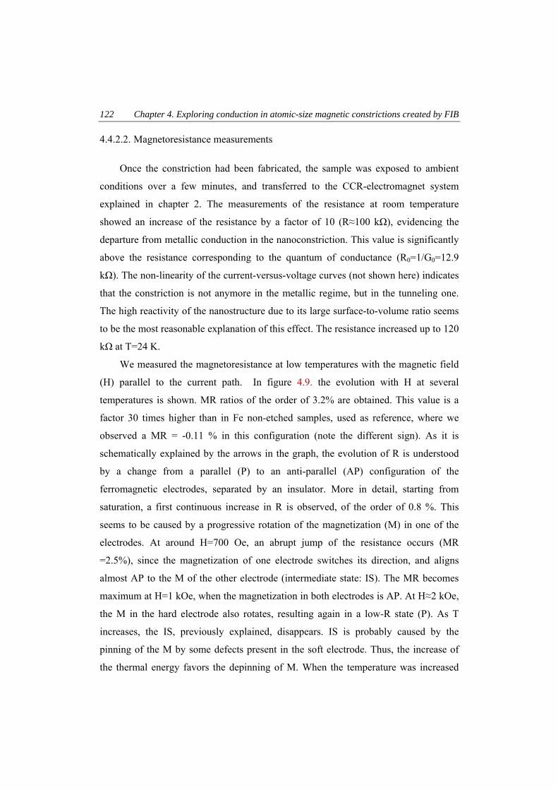
122 Chapter 4. Exploring conduction in atomic-size magnetic constrictions created by FIB
4.4.2.2. Magnetoresistance measurements
Once the constriction had been fabricated, the sample was exposed to ambient
conditions over a few minutes, and transferred to the CCR-electromagnet system
explained in chapter 2. The measurements of the resistance at room temperature
showed an increase of the resistance by a factor of 10 (R≈100 kΩ), evidencing the
departure from metallic conduction in the nanoconstriction. This value is significantly
above the resistance corresponding to the quantum of conductance (R0=1/G0=12.9
kΩ). The non-linearity of the current-versus-voltage curves (not shown here) indicates
that the constriction is not anymore in the metallic regime, but in the tunneling one.
The high reactivity of the nanostructure due to its large surface-to-volume ratio seems
to be the most reasonable explanation of this effect. The resistance increased up to 120
kΩ at T=24 K.
We measured the magnetoresistance at low temperatures with the magnetic field
(H) parallel to the current path. In figure 4.9. the evolution with H at several
temperatures is shown. MR ratios of the order of 3.2% are obtained. This value is a
factor 30 times higher than in Fe non-etched samples, used as reference, where we
observed a MR = -0.11 % in this configuration (note the different sign). As it is
schematically explained by the arrows in the graph, the evolution of R is understood
by a change from a parallel (P) to an anti-parallel (AP) configuration of the
ferromagnetic electrodes, separated by an insulator. More in detail, starting from
saturation, a first continuous increase in R is observed, of the order of 0.8 %. This
seems to be caused by a progressive rotation of the magnetization (M) in one of the
electrodes. At around H=700 Oe, an abrupt jump of the resistance occurs (MR
=2.5%), since the magnetization of one electrode switches its direction, and aligns
almost AP to the M of the other electrode (intermediate state: IS). The MR becomes
maximum at H=1 kOe, when the magnetization in both electrodes is AP. At H≈2 kOe,
the M in the hard electrode also rotates, resulting again in a low-R state (P). As T
increases, the IS, previously explained, disappears. IS is probably caused by the
pinning of the M by some defects present in the soft electrode. Thus, the increase of
the thermal energy favors the depinning of M. When the temperature was increased
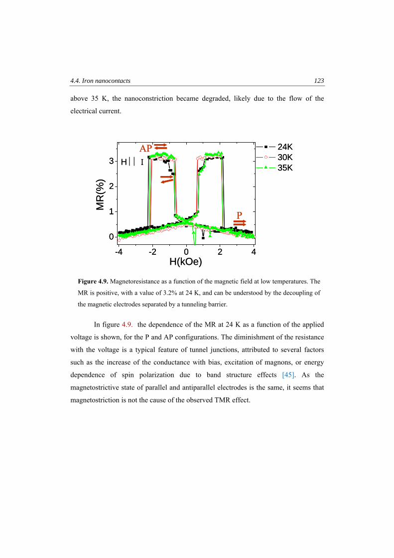
4.4. Iron nanocontacts 123
above 35 K, the nanoconstriction became degraded, likely due to the flow of the
electrical current.
In figure 4.9. the dependence of the MR at 24 K as a function of the applied
voltage is shown, for the P and AP configurations. The diminishment of the resistance
with the voltage is a typical feature of tunnel junctions, attributed to several factors
such as the increase of the conductance with bias, excitation of magnons, or energy
dependence of spin polarization due to band structure effects [45]. As the
magnetostrictive state of parallel and antiparallel electrodes is the same, it seems that
magnetostriction is not the cause of the observed TMR effect.
-4 -2 0 2 4
0
1
2
3
H I
24K 30K 35K
MR
(%)
H(kOe)
P
AP
-4 -2 0 2 4
0
1
2
3
H I
24K 30K 35K
MR
(%)
H(kOe)
P
AP
Figure 4.9. Magnetoresistance as a function of the magnetic field at low temperatures. The
MR is positive, with a value of 3.2% at 24 K, and can be understood by the decoupling of
the magnetic electrodes separated by a tunneling barrier.
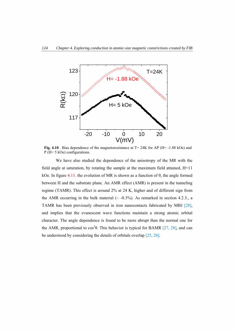
124 Chapter 4. Exploring conduction in atomic-size magnetic constrictions created by FIB
We have also studied the dependence of the anisotropy of the MR with the
field angle at saturation, by rotating the sample at the maximum field attained, H=11
kOe. In figure 4.11. the evolution of MR is shown as a function of θ, the angle formed
between H and the substrate plane. An AMR effect (AMR) is present in the tunneling
regime (TAMR). This effect is around 2% at 24 K, higher and of different sign from
the AMR occurring in the bulk material (~ -0.3%). As remarked in section 4.2.3., a
TAMR has been previously observed in iron nanocontacts fabricated by MBJ [28],
and implies that the evanescent wave functions maintain a strong atomic orbital
character. The angle dependence is found to be more abrupt than the normal one for
the AMR, proportional to cos2θ. This behavior is typical for BAMR [27, 28], and can
be understood by considering the details of orbitals overlap [25, 26].
Fig. 4.10 . Bias dependence of the magnetoresistance at T= 24K for AP (H= -1.88 kOe) and P (H= 5 kOe) configurations.
-20 -10 0 10 20
117
120
123
H= 5 kOe
H= -1.88 kOe
R
(kΩ
)
V(mV)
T=24K
4.4. Iron nanocontacts 125
The experiments as a function of angle are also helpful to discard that
magnetostriction effects are responsible of the observed MR. The magnetostriction in
iron is given by:
)31(cos
23 2 −=
Δ θλSll
(4.7.)
with Δl/l = -7 × 10⁻⁶ for θ = 0º, and Δl/l = 3.5 × 10⁻⁶ for θ = 90º.
Thus, the increase of the MR as a function of θ has a contrary sign that if it was
caused by magnetostriction, where the minimum resistance would be expected when
H is perpendicular to the substrate plane.
The results for this sample are an example of the behavior of all samples we have
created. Although it is possible to fabricate Fe nanoconstrictions near the ballistic
regime of conductance by the method developed, which are stable inside the FIB
chamber, they are degraded when exposed to ambient conditions, breaking or
oxidizing, changing to the tunneling regime of conductivities. For the sample shown
Fig. 4.11. Angle dependence of the MR for low temperatures. A fixed field, H=11 kOe,
is applied.
0 15 30 45 60 75 90
0.0
0.5
1.0
1.5
2.0
H⊥ substrate plane
24K 30K 35K
M
R(%
)
θ(º)
H || I

126 Chapter 4. Exploring conduction in atomic-size magnetic constrictions created by FIB
here, the TMR ratios at low temperature are 30 times higher than non-etched samples.
We also observe a TAMR effect at low temperatures, of the order of 2%, and with an
angle dependence different from the cos2θ expected for bulk AMR. From these
experiments we also assure that magnetostriction is not playing any role in the
measurements.
This result also evidences a crucial point for FIB fabrication: under low voltages
etching, and with a moderated ion dose, the FIB procedure does not destroy the
magnetic properties of the devices, although more research is required to investigate at
what extent they are affected.
4.6. Conclusions 127
4.5. Conclusions
A new approach to obtain stable atomic-sized contacts at room temperature
under high vacuum has been performed. The combination of the FIB etching, with
simultaneous electrical measurements allows a fine control of the resistance. The steps
in the conductance just prior to the crossover to the tunnelling regime are an indication
of atomic reconstructions. The plateaus at different conductance values are associated
with different atomic configurations in the constriction. The simultaneous imaging of
the etching process via the electron column allows following the formed structure in
real-time.
The constrictions are stable at room temperature and under high vacuum
conditions, proved for Cr and Fe. The possibility of establishing point contacts in a
wide variety of materials under similar conditions is expected with the exposed
methodology. This is not the case for other techniques, which are less flexible with
respect to the used materials and protocols. In our case, the sputtering rate of the
material under etching at the used ion energy seems to be the most relevant factor
together with the ion column current, which influences the ion beam width and the
etching rate. We can forsee great potentialities of this method for the creation of
functional devices in the field of Spintronics.
In the case of Fe nanocontacts, the difficulty to have stable nanocontacts when
exposed to ambient conditions has been shown. In spite of the protective covering, the
constrictions are either completely degraded, or in the tunneling regime when they get
in contact with air.
We have shown an example of one iron contact presenting tunneling
conduction. It has TMR ratios at low temperature 30 times higher than non-etched
samples. We also observe a TAMR effect at low temperatures, of the order of 2%, and
with an angle dependence different from the cos2θ expected for bulk AMR. From
these experiments we also assure that magnetostriction is not playing any role in the
measurements. This result shows that under low voltages etching, and with a
128 Chapter 4. Exploring conduction in atomic-size magnetic constrictions created by FIB
moderated ion dose, the FIB procedure does not destroy the magnetic properties of the
devices, although more research is required to investigate at what extent they are
affected. The high stability expected for these constrictions in comparison with other
suspended atomic-size structures, makes this result promising for future research. A
systematic study of the MR is currently under progress to improve the stabilization of
constrictions in the metallic range of resistances, and investigate if high BMR and
BAMR values can be attained at room temperature, which would have high impact in
the field.
We should also remark that a different approach has been developed in our
laboratory during this thesis [46], following the same philosophy that the method
exposed in this chapter. The main advantage is the well-defined current direction
attained, suitable for anisotropic magnetoresistance measurements. However, it is
performed at 30 kV, inducing a higher amount of amorphization [41], with a possible
increase of the degree of deterioration of the magnetic properties. For details see
reference 46.
Chapter 5
1. Pt-C nanowires created by FIBID
and FEBID
In this chapter we will present a thorough characterization of the electrical properties
of Pt-C nanowires created by FIBID and FEBID. The same methodology as in chapter
4 will be used, where the resistance of the NWs is probed as the NW is being grown,
getting a perfect control of the process. The electrical properties are studied at room
temperature, “in situ”, and as a function of temperature, “ex situ”. These results are
correlated with chemical and microstructural characterization, and can be understood
within the framework of the theory by Mott and Anderson for disordered materials.
The chapter is mainly devoted to the study of wires created by FIB. By depositing
NWs with different thicknesses, we study deposits in different ranges of conductivity.
These NWs present a metal-insulator transition as a function of thickness, with the
metal-carbon proportion as the key parameter that determines the mechanism for
electrical conduction.
Besides, this same methodology has been used to compare NWs grown by FIBID in
the metallic regime of conduction with wires grown by FEBID. The deposits induced
by electrons are orders of magnitude more resistive than those induced by ions for all
thicknesses, resembling Pt-C FIBID NWs in the insulating regime of conduction. The
substantial differences in the electrical transport measurements between both types of
deposits can be understood by means of the theories detailed for FIBID-NWs, giving
rise to a complete picture for Pt-C deposits grown by focused beams.
130 Chapter 5. Pt-C nanowires created by FIBID and FEBID
5.1. Nanowires created by Focused-Ion-Beam-Induced-Deposition (FIBID)
5.1.1. Previous results in Pt-C nanodeposits grown by FIBID
One of the most commonly deposited metallic materials using FIBID is Pt. A lot
of work has been done regarding its electrical transport properties, with a wide range
of reported results on the resistivity at room temperature (ρRT), as well as on the
thermal dependence of the resistance, as pointed out in reference 1. We show in table
5.I. the results compiled in that work, together with additional references [1-12]. In
addition to the value for ρRT, we also include, when reported, the thermal coefficient of
the resistivity (β=dρ/dT), the residual resistivity ratio (RRR= ρRT/ρlowT), the electronic
mechanism proposed for conduction, the character of current-versus-voltage curves,
the chemical composition of the deposits, and the gas precursor used. As revealed by
Transmission Electron Microscopy, the microstructure found rather inhomogeneous,
with crystalline metallic inclusions (around 3-10 nm) embedded in an amorphous
carbon matrix [1-5, 9] (see section 5.2.2.3). An important point that is usually missed
when comparing these results is the two types of precursors used for Pt deposition. We
can see that in two groups [3-5 and 10], the nanowires (NWs) are deposited with
cyclopentadienyl-trimethyl platinum, (CH3)3PtCp, whereas in the rest of groups [1, 2,
6-9, 11, 12] methylcyclopentadienyl-trimethyl platinum, (CH3)3Pt(CpCH3) is used.
Deposits using the first precursor (one carbon less present in the molecule) have the
lowest resistivity reported (only about 7 times higher than that of bulk Pt) and a
positive β. At low temperatures they present deviations from the behavior expected for
pure Pt NWs, such as weak antilocalization and quasi-one- dimensional-interference
effects [3-5]. On the contrary, with the second precursor, β is always negative, either
with an appreciable thermal dependence, associated with variable-range hopping
(VRH) [2, 12], or an almost-negligible dependence [1, 9, 10], resembling the
conduction of a dirty metal, with metallic [9] or tunneling conduction [1]. In this
work, we center our study on NWs created with the second precursor, of more
extended use in the scientific community, with the aim to clear up the, in principle,
contradictory reported results.
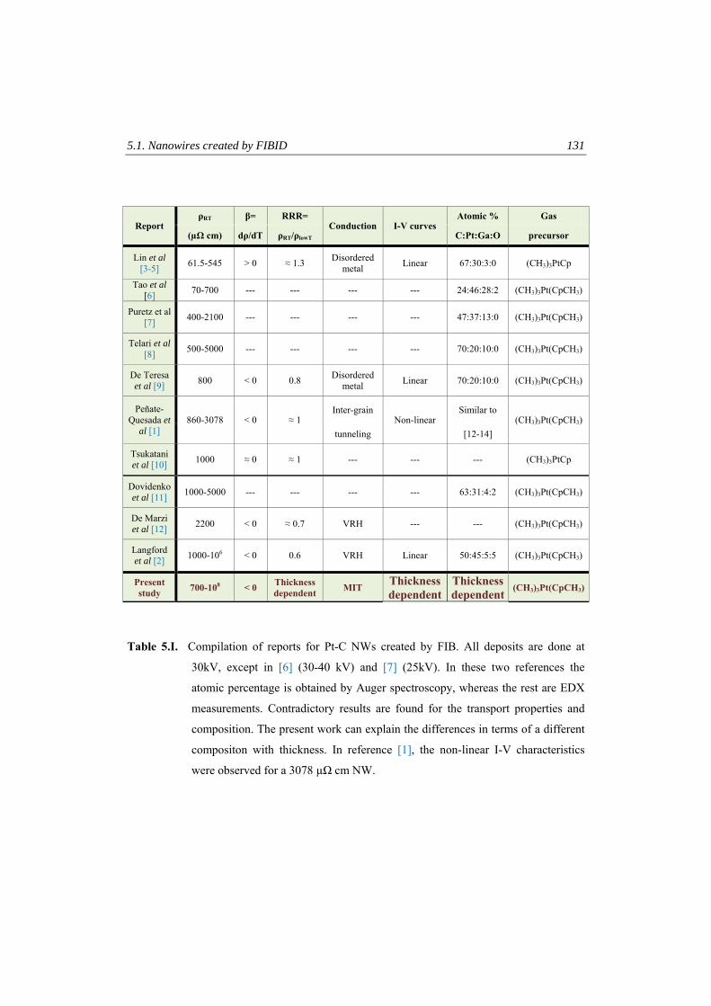
5.1. Nanowires created by FIBID 131
Report ρRT β= RRR=
Conduction I-V curves Atomic % Gas
(µΩ cm) dρ/dT ρRT/ρlowT C:Pt:Ga:O precursor
Lin et al [3-5] 61.5-545 > 0 ≈ 1.3 Disordered
metal Linear 67:30:3:0 (CH3)3PtCp
Tao et al [6] 70-700 --- --- --- --- 24:46:28:2 (CH3)3Pt(CpCH3)
Puretz et al [7] 400-2100 --- --- --- --- 47:37:13:0 (CH3)3Pt(CpCH3)
Telari et al [8] 500-5000 --- --- --- --- 70:20:10:0 (CH3)3Pt(CpCH3)
De Teresa et al [9] 800 < 0 0.8 Disordered
metal Linear 70:20:10:0 (CH3)3Pt(CpCH3)
Peñate-Quesada et
al [1] 860-3078 < 0 ≈ 1
Inter-grain Non-linear
Similar to (CH3)3Pt(CpCH3)
tunneling [12-14]
Tsukatani et al [10] 1000 ≈ 0 ≈ 1 --- --- --- (CH3)3PtCp
Dovidenko et al [11] 1000-5000 --- --- --- --- 63:31:4:2 (CH3)3Pt(CpCH3)
De Marzi et al [12] 2200 < 0 ≈ 0.7 VRH --- --- (CH3)3Pt(CpCH3)
Langford et al [2] 1000-106 < 0 0.6 VRH Linear 50:45:5:5 (CH3)3Pt(CpCH3)
Present study 700-108 < 0 Thickness
dependent MIT Thickness dependent
Thickness dependent (CH3)3Pt(CpCH3)
Table 5.I. Compilation of reports for Pt-C NWs created by FIB. All deposits are done at
30kV, except in [6] (30-40 kV) and [7] (25kV). In these two references the
atomic percentage is obtained by Auger spectroscopy, whereas the rest are EDX
measurements. Contradictory results are found for the transport properties and
composition. The present work can explain the differences in terms of a different
compositon with thickness. In reference [1], the non-linear I-V characteristics
were observed for a 3078 µΩ cm NW.
132 Chapter 5. Pt-C nanowires created by FIBID and FEBID
5.1.2. Experimental details
5.1.2.1. Deposition parameters
The Pt-C NWs were grown using the FIB column integrated in the Dual Beam
system, together with the automatic Gas Injection System (GIS) to introduce the gas
into the process chamber, all explained in detail in section 2. The SEM was used for
imaging the sample, minimizing the ion dose in the deposits. The deposition
parameters are: (CH3)3Pt(CpCH3) precursor gas, (TG) = 35 ºC precursor temperature,
(VFIB) = 30 kV beam voltage, (IFIB) = 10 pA beam current, substrate temperature = 22
ºC, dwell time = 200 ns, chamber base pressure = 10-7 mbar, process pressure = 3 ×
10-6 mbar, beam overlap = 0 %, distance between GIS needle and substrate (LD) = 1.5
mm . Under these conditions, a dose of 3 × 10¹⁶ ion / cm2-min roughly irradiates the
sample. We must emphasize that the values for TG (about 10 ºC below the usual
operation temperature) and LD (~1.35 mm higher than usually) were chosen to
decrease the deposition rate, allowing detailed measurements of the evolution of the
resistance as the deposit was realized. This is required to get fine control, especially
during the initial stages, where a very abrupt change in the resistance occurs in a very
short period of time (see section 5.3). We obtained approximately the same final
resistivity when depositing NWs using normal conditions (see section 5.2.1), so these
changes do not seem to affect substantially the properties of the NWs. Thermally-
oxidized silicon (~200 nm of SiO2) was used as substrate, and aluminium pads were
previously patterned by optical lithography (see lift-off process in section 2.1.1. for
details). The studied NWs (top-bottom deposit in figure 5.1(b)) are length (L) = 15
µm, width (w) = 500 nm, thickness (t) = variable with process time.
5.1.2.2. “In situ” measurement of the resistance during the growth process
The electrical resistance was measured inside the process chamber using the
experimental setup explained in detail in section 2.2.2. In figure 5.1(a), a SEM image
shows the experimental configuration for the deposition, where the 4 microprobes are
contacted to the pads, and the GIS needle is inserted near the substrate. By applying a
constant current between the two extremes of the NW, and measuring the voltage drop
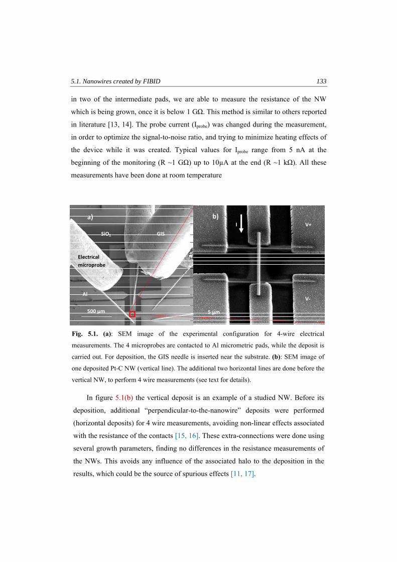
5.1. Nanowires created by FIBID 133
in two of the intermediate pads, we are able to measure the resistance of the NW
which is being grown, once it is below 1 GΩ. This method is similar to others reported
in literature [13, 14]. The probe current (Iprobe) was changed during the measurement,
in order to optimize the signal-to-noise ratio, and trying to minimize heating effects of
the device while it was created. Typical values for Iprobe range from 5 nA at the
beginning of the monitoring (R ~1 GΩ) up to 10µA at the end (R ~1 kΩ). All these
measurements have been done at room temperature
In figure 5.1(b) the vertical deposit is an example of a studied NW. Before its
deposition, additional “perpendicular-to-the-nanowire” deposits were performed
(horizontal deposits) for 4 wire measurements, avoiding non-linear effects associated
with the resistance of the contacts [15, 16]. These extra-connections were done using
several growth parameters, finding no differences in the resistance measurements of
the NWs. This avoids any influence of the associated halo to the deposition in the
results, which could be the source of spurious effects [11, 17].
500 µm 5 µm
a) b)
GIS
Electrical microprobe
I V+
V‐
SiO2
Al
Fig. 5.1. (a): SEM image of the experimental configuration for 4-wire electrical
measurements. The 4 microprobes are contacted to Al micrometric pads, while the deposit is
carried out. For deposition, the GIS needle is inserted near the substrate. (b): SEM image of
one deposited Pt-C NW (vertical line). The additional two horizontal lines are done before the
vertical NW, to perform 4 wire measurements (see text for details).
134 Chapter 5. Pt-C nanowires created by FIBID and FEBID
5.1.2.3. Compositional analysis by EDX
For the study of the composition by Energy Dispersive X-Ray (EDX), we
performed deposits on SiO2 of the same lateral dimensions as those used for electrical
measurements, and varying thickness. The EDX measurements were done by means of
a commercial Oxford INCA 200 EDX setup whose detector is driven in the vicinity of
the sample. The selected energy for the microanalysis is 20kV. Prior to each EDX
experiment, energy calibration by means of a Co calibration sample was done.
5.1.2.4. Structural analysis via Scanning-Transmission-Electron-Microscopy
Cross-section lamella of selected NWs was performed with the dual beam
equipment by means of Ga ion thinning initially at 30 kV and finally at 5 kV. An
Omniprobe nanomanipulator was used to perform in-situ lift-out and placing of the
lamella on a Cu grid. The STEM images were obtained inside the same experimental
setup, in Dark Field mode, under 30 kV and 0.15 nA conditions.
5.1.2.5. XPS measurements
In order to study the chemical nature of the deposits, we have done depth-profile
X-ray Photoelectron Spectroscopy (XPS) measurements in an Axis Ultra equipment
by Kratos, at a base pressure of 3 × 10⁻¹⁰ Torr. Because of the limited spatial resolution
of the X-ray probe, this deposit was much larger in comparison with all the others:
length = 100µm × width = 100µm × thickness = 200nm. Under the chosen conditions,
previously detailed, this would imply a process time of about 25 hours, so we changed
the IBEAM to 3 nA, reducing significantly the deposition time. The dose rate, ~1016
ions/cm2-min, was approximately the same in both types of experiments. A 5 kV-
argon etching, with current densities of the order of 0.15 A/m2 was done, to obtain a
XPS depth profile of the deposits (probing every 30 nm).
For the quantitative analysis of the XPS spectra, a Shirley-type background was
subtracted, using pseudo-Voigt peak profiles with a 10-30 % Lorentzian contribution
in all edges, except for the Pt 4f. In this case, because of the asymmetry of the peaks,
5.1. Nanowires created by FIBID 135
the spectra were analyzed using the Doniach - Sunjic function [18]:
⎟⎠⎞
⎜⎝⎛ +
+−Γ
= − )(21cos
)()1()( 2/)1(22 εθπα
γεαε αI (5.1.a)
( )γεαεθ /tan)1()( 1−+= (5.1.b)
where ε is the energy measured relative to Fermi energy, Γ is the gamma function, γ is
the natural linewidth of the hole state corresponding to its lifetime, and α is the line
asymmetry parameter. The function was convoluted with a Gaussian curve with
FWHM = 0.3 eV, to take into account the experimental broadening (instrumental
resolution, sample inhomogeneity, etc) [19].
5.1.2.6. Transport measurements as a function of temperature
The measurements of the electrical resistance as a function of temperature were
performed in the closed-cycle refrigerator detailed in section 2.2.1.
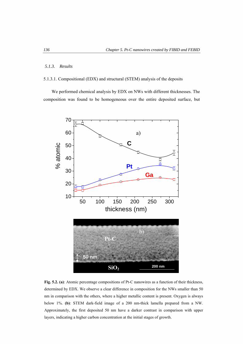
136 Chapter 5. Pt-C nanowires created by FIBID and FEBID
5.1.3. Results
5.1.3.1. Compositional (EDX) and structural (STEM) analysis of the deposits
We performed chemical analysis by EDX on NWs with different thicknesses. The
composition was found to be homogeneous over the entire deposited surface, but
50 100 150 200 250 30010
20
30
40
50
60
70
% a
tom
ic
thickness (nm)
C
PtGa
a)
thickness
50 nm
200 nm
thickness
50 nm
200 nm
b) Pt-C
SiO2
Fig. 5.2. (a): Atomic percentage compositions of Pt-C nanowires as a function of their thickness,
determined by EDX. We observe a clear difference in composition for the NWs smaller than 50
nm in comparison with the others, where a higher metallic content is present. Oxygen is always
below 1%. (b): STEM dark-field image of a 200 nm-thick lamella prepared from a NW.
Approximately, the first deposited 50 nm have a darker contrast in comparison with upper
layers, indicating a higher carbon concentration at the initial stages of growth.
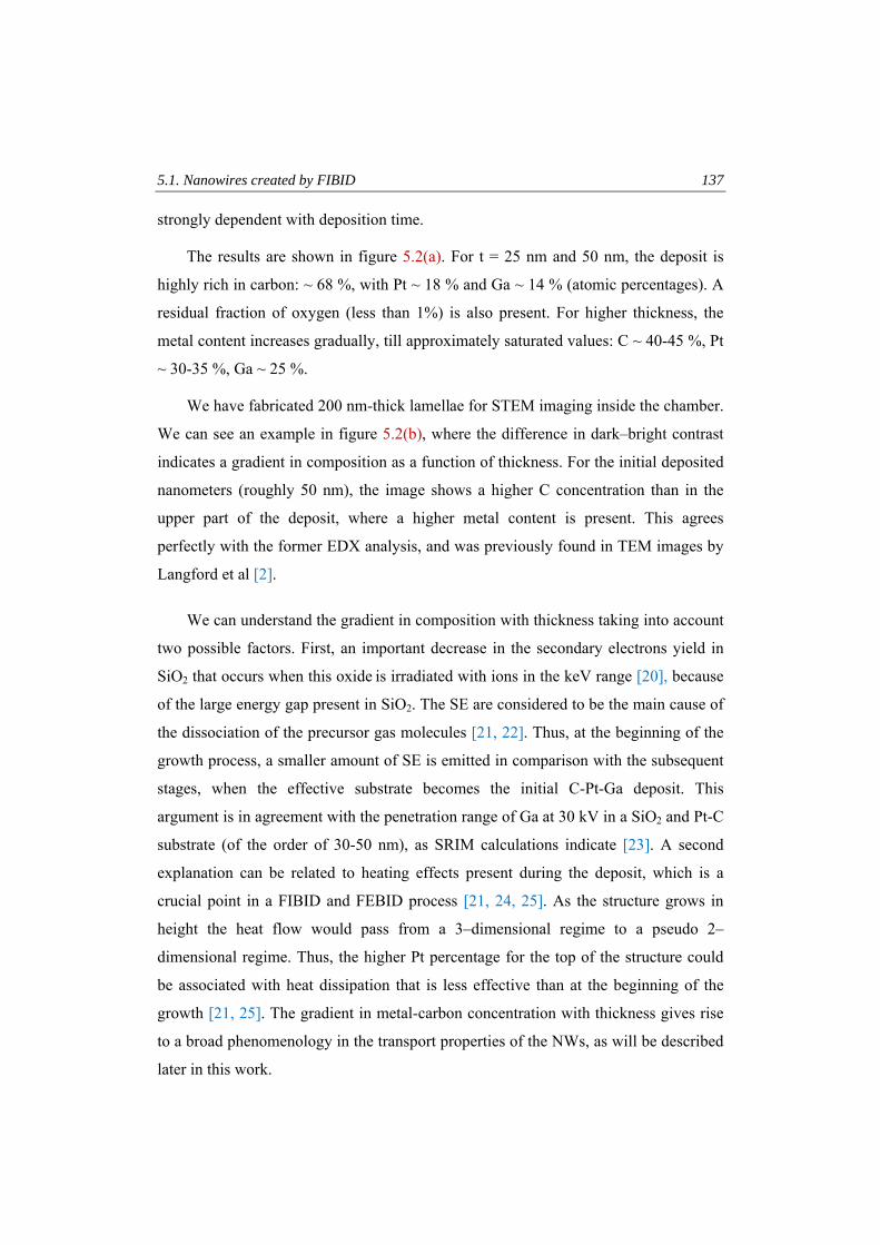
5.1. Nanowires created by FIBID 137
strongly dependent with deposition time.
The results are shown in figure 5.2(a). For t = 25 nm and 50 nm, the deposit is
highly rich in carbon: ~ 68 %, with Pt ~ 18 % and Ga ~ 14 % (atomic percentages). A
residual fraction of oxygen (less than 1%) is also present. For higher thickness, the
metal content increases gradually, till approximately saturated values: C ~ 40-45 %, Pt
~ 30-35 %, Ga ~ 25 %.
We have fabricated 200 nm-thick lamellae for STEM imaging inside the chamber.
We can see an example in figure 5.2(b), where the difference in dark–bright contrast
indicates a gradient in composition as a function of thickness. For the initial deposited
nanometers (roughly 50 nm), the image shows a higher C concentration than in the
upper part of the deposit, where a higher metal content is present. This agrees
perfectly with the former EDX analysis, and was previously found in TEM images by
Langford et al [2].
We can understand the gradient in composition with thickness taking into account
two possible factors. First, an important decrease in the secondary electrons yield in
SiO2 that occurs when this oxide is irradiated with ions in the keV range [20], because
of the large energy gap present in SiO2. The SE are considered to be the main cause of
the dissociation of the precursor gas molecules [21, 22]. Thus, at the beginning of the
growth process, a smaller amount of SE is emitted in comparison with the subsequent
stages, when the effective substrate becomes the initial C-Pt-Ga deposit. This
argument is in agreement with the penetration range of Ga at 30 kV in a SiO2 and Pt-C
substrate (of the order of 30-50 nm), as SRIM calculations indicate [23]. A second
explanation can be related to heating effects present during the deposit, which is a
crucial point in a FIBID and FEBID process [21, 24, 25]. As the structure grows in
height the heat flow would pass from a 3–dimensional regime to a pseudo 2–
dimensional regime. Thus, the higher Pt percentage for the top of the structure could
be associated with heat dissipation that is less effective than at the beginning of the
growth [21, 25]. The gradient in metal-carbon concentration with thickness gives rise
to a broad phenomenology in the transport properties of the NWs, as will be described
later in this work.
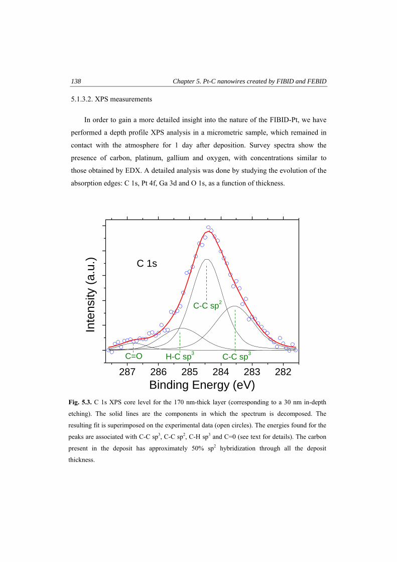
138 Chapter 5. Pt-C nanowires created by FIBID and FEBID
5.1.3.2. XPS measurements
In order to gain a more detailed insight into the nature of the FIBID-Pt, we have
performed a depth profile XPS analysis in a micrometric sample, which remained in
contact with the atmosphere for 1 day after deposition. Survey spectra show the
presence of carbon, platinum, gallium and oxygen, with concentrations similar to
those obtained by EDX. A detailed analysis was done by studying the evolution of the
absorption edges: C 1s, Pt 4f, Ga 3d and O 1s, as a function of thickness.
287 286 285 284 283 282H-C sp3
In
tens
ity (a
.u.) C 1s
Binding Energy (eV)
C-C sp2
C-C sp3C=O
Fig. 5.3. C 1s XPS core level for the 170 nm-thick layer (corresponding to a 30 nm in-depth
etching). The solid lines are the components in which the spectrum is decomposed. The
resulting fit is superimposed on the experimental data (open circles). The energies found for the
peaks are associated with C-C sp3, C-C sp2, C-H sp3 and C=0 (see text for details). The carbon
present in the deposit has approximately 50% sp2 hybridization through all the deposit
thickness.
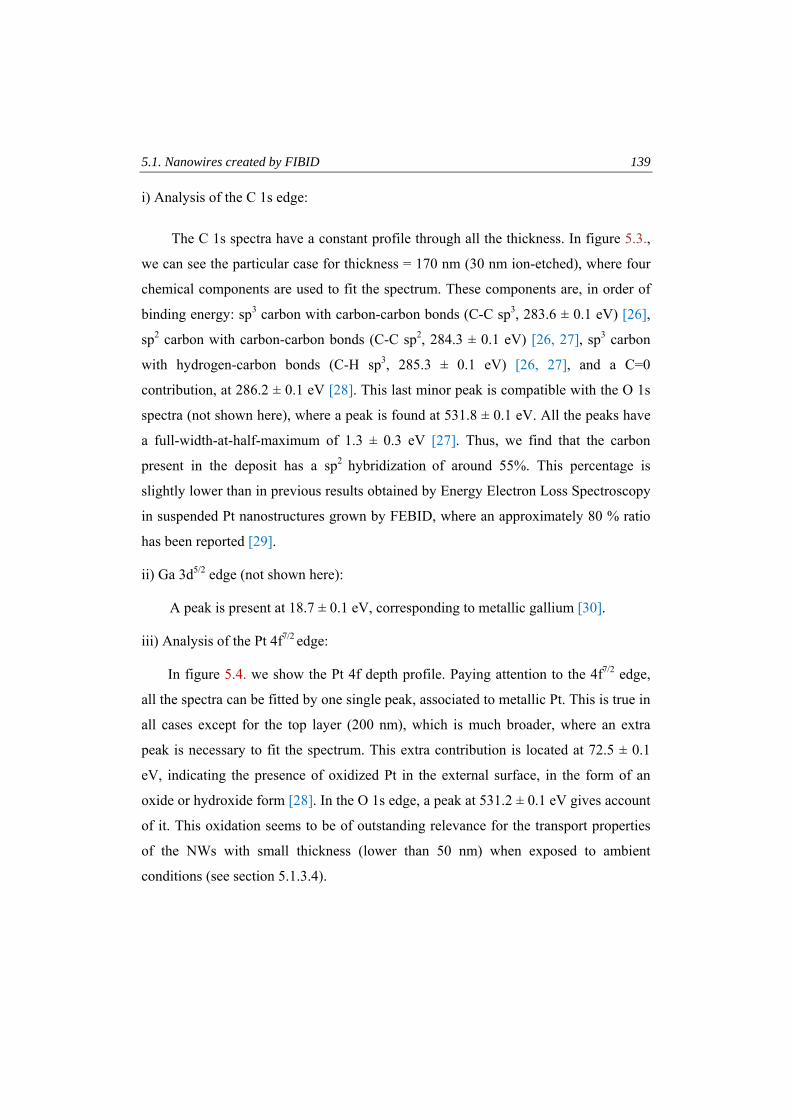
5.1. Nanowires created by FIBID 139
i) Analysis of the C 1s edge:
The C 1s spectra have a constant profile through all the thickness. In figure 5.3.,
we can see the particular case for thickness = 170 nm (30 nm ion-etched), where four
chemical components are used to fit the spectrum. These components are, in order of
binding energy: sp3 carbon with carbon-carbon bonds (C-C sp3, 283.6 ± 0.1 eV) [26],
sp2 carbon with carbon-carbon bonds (C-C sp2, 284.3 ± 0.1 eV) [26, 27], sp3 carbon
with hydrogen-carbon bonds (C-H sp3, 285.3 ± 0.1 eV) [26, 27], and a C=0
contribution, at 286.2 ± 0.1 eV [28]. This last minor peak is compatible with the O 1s
spectra (not shown here), where a peak is found at 531.8 ± 0.1 eV. All the peaks have
a full-width-at-half-maximum of 1.3 ± 0.3 eV [27]. Thus, we find that the carbon
present in the deposit has a sp2 hybridization of around 55%. This percentage is
slightly lower than in previous results obtained by Energy Electron Loss Spectroscopy
in suspended Pt nanostructures grown by FEBID, where an approximately 80 % ratio
has been reported [29].
ii) Ga 3d5/2 edge (not shown here):
A peak is present at 18.7 ± 0.1 eV, corresponding to metallic gallium [30].
iii) Analysis of the Pt 4f7/2 edge:
In figure 5.4. we show the Pt 4f depth profile. Paying attention to the 4f7/2 edge,
all the spectra can be fitted by one single peak, associated to metallic Pt. This is true in
all cases except for the top layer (200 nm), which is much broader, where an extra
peak is necessary to fit the spectrum. This extra contribution is located at 72.5 ± 0.1
eV, indicating the presence of oxidized Pt in the external surface, in the form of an
oxide or hydroxide form [28]. In the O 1s edge, a peak at 531.2 ± 0.1 eV gives account
of it. This oxidation seems to be of outstanding relevance for the transport properties
of the NWs with small thickness (lower than 50 nm) when exposed to ambient
conditions (see section 5.1.3.4).
140 Chapter 5. Pt-C nanowires created by FIBID and FEBID
For the rest of Pt 4f spectra, we can see substantial differences with thickness.
First, a progressive shift towards higher binding energies (BE) occurs from the more
external part of the deposit (170 nm) to the more internal one (20 nm) (see oblique
line). For the 170 nm spectrum, the maximum is located at 70.7 ± 0.1 eV. This BE
matches the range typically found at the surface of Pt crystals [31]. For the 20 nm
spectrum, the maximum shifts in BE to the value of 71.2 ± 0.1 eV. The second
76 74 72 70
Metallic Pt
Oxidized Pt
Pt 4f200nm
170nm140nm110nm80nm50nm
In
tens
ity (a
.u.)
Binding Energy (eV)
20nm
Fig. 5.4. Pt 4f core level XPS depth profile. Successive spectra were obtained after a 30 nm
argon etching process. The numbers in the figure refer to the remaining sample thickness.
The external surface of the deposit presents a broader spectrum than the rest, as a
consequence of an extra peak present, associated with platinum oxide or hydroxide (left
dashed line). For the rest of surfaces, the spectra can be fitted by only one contribution,
associated to metallic platinum. This peak presents a shift towards lower binding energies as
the probed layer is increasingly internal (oblique, right dashed line), as well as a decrease in
the asymmetry of the Pt 4f peak. We correlate this evolution with thickness with a
progressive increase of the cluster sizes as the deposit gets thicker
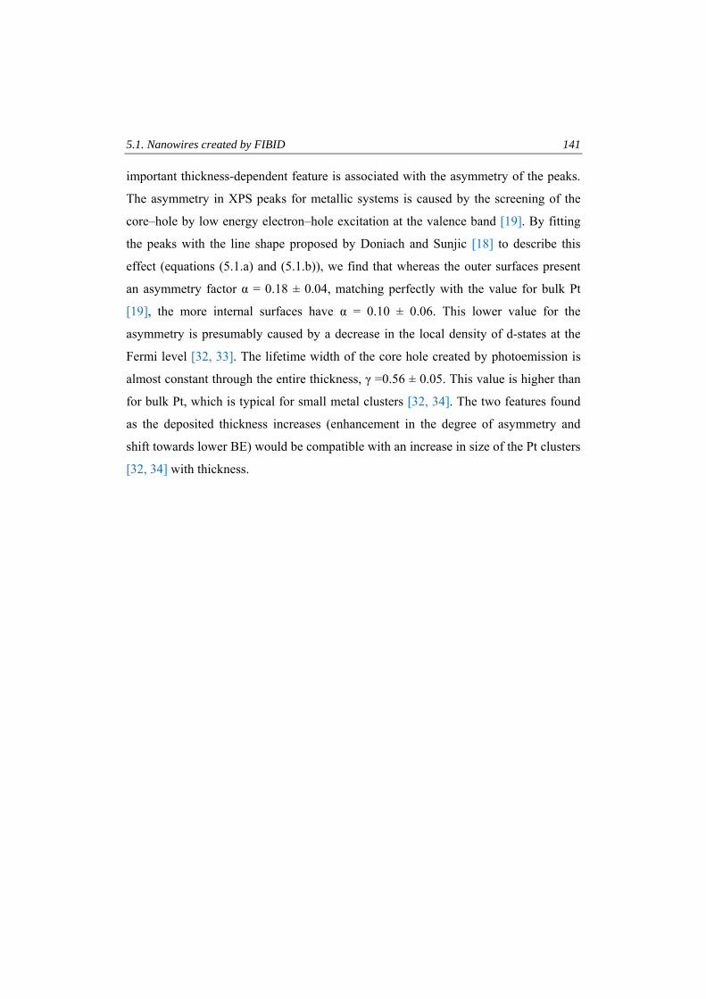
5.1. Nanowires created by FIBID 141
important thickness-dependent feature is associated with the asymmetry of the peaks.
The asymmetry in XPS peaks for metallic systems is caused by the screening of the
core–hole by low energy electron–hole excitation at the valence band [19]. By fitting
the peaks with the line shape proposed by Doniach and Sunjic [18] to describe this
effect (equations (5.1.a) and (5.1.b)), we find that whereas the outer surfaces present
an asymmetry factor α = 0.18 ± 0.04, matching perfectly with the value for bulk Pt
[19], the more internal surfaces have α = 0.10 ± 0.06. This lower value for the
asymmetry is presumably caused by a decrease in the local density of d-states at the
Fermi level [32, 33]. The lifetime width of the core hole created by photoemission is
almost constant through the entire thickness, γ =0.56 ± 0.05. This value is higher than
for bulk Pt, which is typical for small metal clusters [32, 34]. The two features found
as the deposited thickness increases (enhancement in the degree of asymmetry and
shift towards lower BE) would be compatible with an increase in size of the Pt clusters
[32, 34] with thickness.
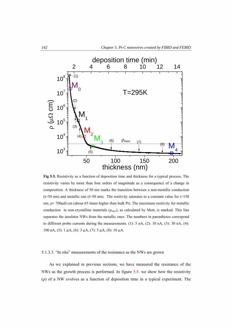
142 Chapter 5. Pt-C nanowires created by FIBID and FEBID
5.1.3.3. “In situ” measurements of the resistance as the NWs are grown
As we explained in previous sections, we have measured the resistance of the
NWs as the growth process is performed. In figure 5.5. we show how the resistivity
(ρ) of a NW evolves as a function of deposition time in a typical experiment. The
50 100 150 200103
104
105
106
107
108
2 4 6 8 10 12 14
(8)(7)(6)
(5)
(3)
(1)
M2
M1
deposition time (min)ρ
(μΩ
cm
)
thickness (nm)
M0 T=295K
R=200 rho(μΩcm)/t(nm)
M3 M4
(2)
(4)ρmax
Fig 5.5. Resistivity as a function of deposition time and thickness for a typical process. The
resistivity varies by more than four orders of magnitude as a consequence of a change in
composition. A thickness of 50 nm marks the transition between a non-metallic conduction
(t<50 nm) and metallic one (t>50 nm). The resitivity saturates to a constant value for t>150
nm, ρ≈ 700µΩ cm (about 65 times higher than bulk Pt). The maximum resitivity for metallic
conduction in non-crystalline materials (ρmax), as calculated by Mott, is marked. This line
separates the insulator NWs from the metallic ones. The numbers in parentheses correspond
to different probe currents during the measurements. (1): 5 nA, (2): 10 nA, (3): 30 nA, (4):
100 nA, (5): 1 µA, (6): 3 µA, (7): 5 µA, (8): 10 µA.
5.1. Nanowires created by FIBID 143
results were reproduced over several experiments.
The highest value for ρ corresponds to ~1 GΩ in resistance, and to ~1 kΩ for the
lowest value. We have correlated the process time (Tp) with the deposited thickness by
doing cross-section inspections of NWs created at different times. Thus, we can also
express the results in terms of resistivity, by using the relation:
LtwR ×
=ρ (5.2.)
We can see that under these conditions the resistivity of the NWs starts from a
value above 108 µΩ cm. An abrupt decrease is produced as the thickness increases,
lowering its resistivity in 4 orders of magnitude when the thickness reaches 50 nm.
From that moment on, ρ decreases slightly, saturating to a constant value of ~ 700
µΩcm (around 65 times higher than the value for bulk Pt) for t> 150 nm. The
negligible thickness dependence of ρ for thickness >50 nm was previously evidenced
in reference 15. We have not observed any increase in ρ for long Tp as a consequence
of the disorder created by ions, such as that reported for W and Pd-FIBID [13]. This
procedure has been repeated many times (~10), the behavior being the same in all
cases. From these experiments, we conclude that the resistivity at room temperature is
highly dependent on the NW thickness. This result explains the large diversity of
values for ρRT of FIBID-Pt NWs reported in the literature [1-12]. We must emphasize
that the chosen parameters are of great importance in the particular values of the
resistivity for a given thickness, since effects such as heating, diffusion, interaction of
the beam with substrate, etc, can differ depending on the conditions. We are not able
to reach resistivities as low as the ones reported by Lin et al [3-9]. The different
precursor gas used for deposition, as it was pointed out in section 5.1.1., seems to be
the most probable reason for it. The resistivity as a function of thickness crosses the
value reported by Mott for the maximum metallic resistivity for a non-crystalline
material, ρmax≈ 3000 µΩcm [35] at ≈50 nm (see dashed line in figure 5.5). Taking into
account this criterion, we would roughly expect a non-metallic conduction for samples
with ρ>ρmax, and a metallic conduction for ρ<ρmax.
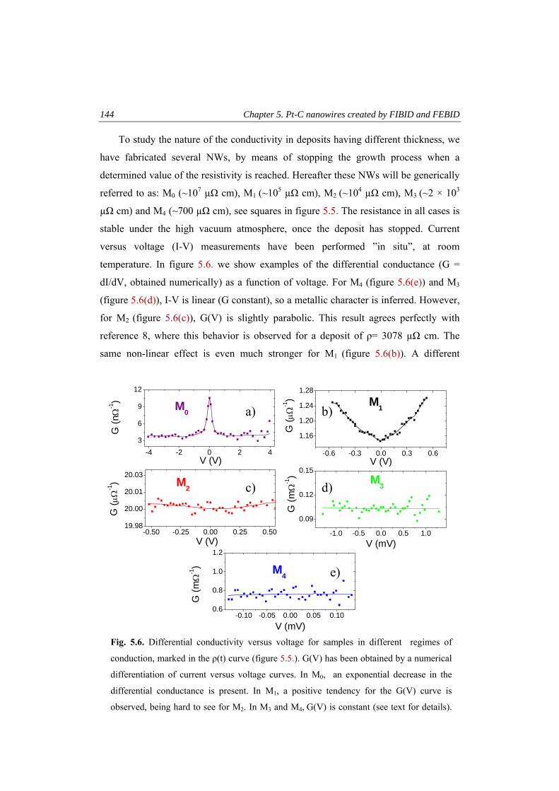
144 Chapter 5. Pt-C nanowires created by FIBID and FEBID
To study the nature of the conductivity in deposits having different thickness, we
have fabricated several NWs, by means of stopping the growth process when a
determined value of the resistivity is reached. Hereafter these NWs will be generically
referred to as: M0 (~107 µΩ cm), M1 (~105 µΩ cm), M2 (~104 µΩ cm), M3 (~2 × 10³
µΩ cm) and M4 (~700 µΩ cm), see squares in figure 5.5. The resistance in all cases is
stable under the high vacuum atmosphere, once the deposit has stopped. Current
versus voltage (I-V) measurements have been performed ”in situ”, at room
temperature. In figure 5.6. we show examples of the differential conductance (G =
dI/dV, obtained numerically) as a function of voltage. For M4 (figure 5.6(e)) and M3
(figure 5.6(d)), I-V is linear (G constant), so a metallic character is inferred. However,
for M2 (figure 5.6(c)), G(V) is slightly parabolic. This result agrees perfectly with
reference 8, where this behavior is observed for a deposit of ρ= 3078 µΩ cm. The
same non-linear effect is even much stronger for M1 (figure 5.6(b)). A different
-4 -2 0 2 43
6
9
12
-0.6 -0.3 0.0 0.3 0.6
1.16
1.20
1.24
1.28
-0.50 -0.25 0.00 0.25 0.5019.98
20.00
20.01
20.03
-1.0 -0.5 0.0 0.5 1.0
0.09
0.12
0.15
-0.10 -0.05 0.00 0.05 0.100.6
0.8
1.0
1.2
G (μ
Ω-1)
M4
M3M2
M1
G (n
Ω-1)
V (V)
M0
V (V)
G (m
Ω-1)
G (m
Ω-1)
G (μ
Ω-1)
V (V)
V (mV)
V (mV)
a) b)
c) d)
e)
Fig. 5.6. Differential conductivity versus voltage for samples in different regimes of
conduction, marked in the ρ(t) curve (figure 5.5.). G(V) has been obtained by a numerical
differentiation of current versus voltage curves. In M0, an exponential decrease in the
differential conductance is present. In M1, a positive tendency for the G(V) curve is
observed, being hard to see for M2. In M3 and M4, G(V) is constant (see text for details).
5.1. Nanowires created by FIBID 145
behavior in G(V) occurs for the most resistive sample, M0 (fig. 5.6(a)), where a peak
in the differential conductance is found at low bias, decreasing from ~ 10 nΩ-1 to a
constant value of 4 nΩ-1 for voltages higher than 0.5 V. G(V) measurements confirm
Mott’s criterion for the maximum resistivity for metallic conduction in non-crystalline
materials [35]. We discuss in detail the evolution of G(V) with thickness in sections
5.1.3.3 and 5.1.4.
We can understand these strong differences for the electrical transport properties
at room temperature taking into account the results obtained in section 5.1.3.1., where
a gradient in composition is observed for the NWs as a function of thickness. For NWs
thinner than approximately 50 nm, the metal (Pt + Ga) content is lower than 33%
(atomic), resulting in resistivity values orders of magnitude higher than those for pure
Pt, together with non-linear features in the I–V curves. For NWs thicker than 50 nm,
the metal content is higher than 33 %. In this case, the resistivity reaches a minimum
value (about 65 times higher than for Pt), and metallic I–V characteristics are
observed. A more detailed discussion will be presented in section 5.1.4.
5.1.3.4. Temperature dependence of the electrical properties
For a better understanding of the transport mechanisms in the Pt-C NWs, we have
measured the thermal dependence of the resistance, as well as I–V curves at different
temperatures. We have studied NWs in the representative ranges shown in section
5.1.3.3.: M0, M1, M2, M3 and M4. The first substantial difference between samples is
related to the modification of the resistance when the NWs come into contact with
ambient atmosphere. For M4, M3 and M2, we did not observe important changes in R,
whereas for M1 the resistance was roughly doubled, and for M0 it became higher than
1GΩ. These changes are clearly associated with the oxidation effect for Pt at the top
part of the deposits after exposure to ambient conditions (see section 5.1.3.2).
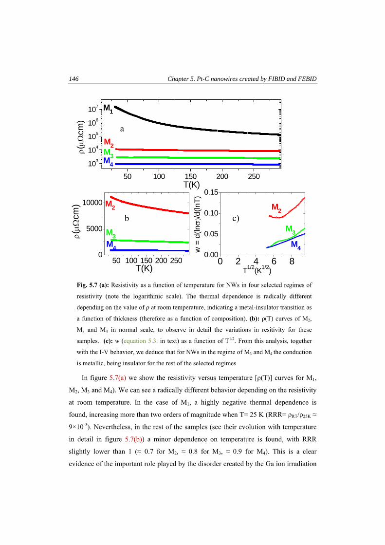
146 Chapter 5. Pt-C nanowires created by FIBID and FEBID
In figure 5.7(a) we show the resistivity versus temperature [ρ(T)] curves for M1,
M2, M3 and M4). We can see a radically different behavior depending on the resistivity
at room temperature. In the case of M1, a highly negative thermal dependence is
found, increasing more than two orders of magnitude when T= 25 K (RRR= ρRT/ρ25K ≈
9×10⁻³). Nevertheless, in the rest of the samples (see their evolution with temperature
in detail in figure 5.7(b)) a minor dependence on temperature is found, with RRR
slightly lower than 1 (≈ 0.7 for M2, ≈ 0.8 for M3, ≈ 0.9 for M4). This is a clear
evidence of the important role played by the disorder created by the Ga ion irradiation
50 100 150 200 250
103
104
105
106
107
50 100 150 200 2500
5000
10000
0 2 4 6 80.00
0.05
0.10
0.15
M4
M3
M4
M3
M2
ρ(μΩ
cm)
T(K)
M4
M3
M2
ρ(μΩ
cm)
T(K)
w =
d(ln
σ)/d
(lnT)
T1/2(K1/2)
M2
M1
a
b c)
Fig. 5.7 (a): Resistivity as a function of temperature for NWs in four selected regimes of
resistivity (note the logarithmic scale). The thermal dependence is radically different
depending on the value of ρ at room temperature, indicating a metal-insulator transition as
a function of thickness (therefore as a function of composition). (b): ρ(T) curves of M2,
M3 and M4 in normal scale, to observe in detail the variations in resitivity for these
samples. (c): w (equation 5.3. in text) as a function of T1/2. From this analysis, together
with the I-V behavior, we deduce that for NWs in the regime of M3 and M4 the conduction
is metallic, being insulator for the rest of the selected regimes
5.1. Nanowires created by FIBID 147
during the growth, as well as by the inhomogeneous nature of the deposit. We must
remark again that a positive thermal coefficient for FIBID-Pt has been shown in
literature [10-12], but using a different gas precursor.
We have used the ρ(T) measurements to determine if the NWs series presents a
metal-insulator transition (MIT) with thickness, by calculating the variable:
( )( )Td
dTwln
ln)(1−
=ρ
(5.3.)
The dependence of w upon T is far more sensitive for determining the transition
than ρ(T), as has been stressed by Möbius et al [36]. w(T→ 0) = 0 implies a metallic
character of the conduction, whereas either a diverging or finite value for w(T→ 0)
indicates that the sample is an insulator. In our case, the lowest temperature attainable
is too high (25 K) to apply this criterion strictly. However, in M2, as shown in figure
5.7(c), w(T) is far from tending to zero, whereas in M3 and M4 the behavior of w(T)
has this tendency. We could then infer that M3 and M4 have metallic conduction, being
insulators for the rest. This is in perfect agreement with the results obtained at room
temperature (see section 5.1.3.2.) and, as will be shown below, with the I-V study
done as a function of temperature. Therefore, the results support a scenario where the
Pt-C NWs grown by FIB present a MIT as a function of thickness (metal/carbon
composition). If a low metal content is present, the conduction is attributable to carrier
hopping into localized states, whereas a high enough amount of metallic inclusions
guarantees that transport will take place by carriers in extended states. This explains
the diversity of results found in literature for the dependence of Pt-FIBID resistivity
with temperature. It should be noticed that amorphous carbon by itself is well known
to present a MIT by tuning the sp2-sp3 ratio [37, 38], but in our case the amount of
metal present in the deposits is the key parameter for determining the mechanism
responsible for conduction.
We have studied in detail ρ(T) in the non-metallic sample M1. By fitting the curve
using an activation dependence:
148 Chapter 5. Pt-C nanowires created by FIBID and FEBID
N
T
T
T⎟⎟⎟
⎠
⎞
⎜⎜⎜
⎝
⎛
∞=
0
exp)( ρρ (5.4.)
it is found that the best exponent N is 0.5. Variable-range hopping (VRH) of electrons
between localized states, as predicted by Mott, has the same functional dependence,
but with N=0.25 [35]. Efros and Shklovskii demonstrated that a VRH process when
the Coulomb interaction between sites is taken into account (ES-VRH) results in a
Coulomb gap, yielding an exponent of 0.5, instead of 0.25 [39]. There exists a critical
temperature Tc above which Mott-VRH is fulfilled, whereas below Tc, Coulomb
interactions become important, and the conduction is by ES-VRH. As discussed in
reference 40 for FEBID-Pt nanostructures, a Tc higher than room temperature is
expected if reasonable assumptions are made for the values of two unknown quantities
in this material: the density of states at the Fermi energy, and the dielectric constant.
The observed thermal dependence of M1 suggests that the same arguments are valid in
this case. We should also mention that ρ(T) in M2 also follows this dependence in the
low T-regime.
We have also performed I-V curves as a function of temperature for all the
samples and, as in the case of measurements inside the chamber, differentiated
numerically the curves to obtain the differential conductance G. First, for M4 and M3,
I-V curves are linear for all temperatures (not shown here), indicating a metallic
character in all the range of T studied. This is not the case for M2 and M1. The results
are in perfect agreement with the w(T) analysis done before.
In the case of M2, we show in figure 5.8. the normalized conductance G/G0 versus
voltage for selected temperatures, where G0 is the lowest value for G. The non-
linearity effects increase as T diminishes, reaching 2 % [100×(G/G0-1)] at 25 K. We
can see that the dependence for this sample is the same as that for the one reported in
reference 1, where the increase in the differential conductance with voltage was
understood in terms of the Glazman-Matveev model [41] for multi-step tunnelling
occurring between the Pt-Ga nanocrystals embedded in the C-insulator matrix. We
will discuss this dependence in section 5.1.4.
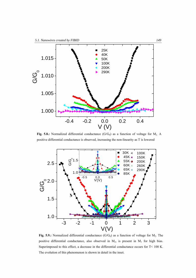
5.1. Nanowires created by FIBID 149
-0.4 -0.2 0.0 0.2 0.4
1.000
1.005
1.010
1.015
V (V)
25K 40K 50K 100K 200K 290K
G/G
0
Fig. 5.8.: Normalized differential conductance (G/G0) as a function of voltage for M2. A
positive differential conductance is observed, increasing the non-linearity as T is lowered
100K 150K 200K 260K 290K
30K 45K 55K 60K 65K 85K
-3 -2 -1 0 1 2 31.0
1.5
2.0
2.5
100K 150K 200K 260K 290K
30K 45K 55K 60K 65K 85K
-0.5 0.0 0.51.0
1.5
G/G
0
V(V)
G/G
0
V(V)
M
Fig. 5.9.: Normalized differential conductance (G/G0) as a function of voltage for M2. The
positive differential conductance, also observed in M2, is present in M1 for high bias.
Superimposed to this effect, a decrease in the differential conductance occurs for T< 100 K.
The evolution of this phenomenon is shown in detail in the inset.
150 Chapter 5. Pt-C nanowires created by FIBID and FEBID
In figure 5.9. we show the normalized conductance for M1. For temperatures
higher than 100 K, the same dependence as in M2 is exhibited. This sample is much
more insulating than M2, so the non-linearity at 100 K, for instance, is around 5%. A
richer behavior is found for temperatures below 100 K. As can be observed, a peak in
G(V) appears at zero bias, as a consequence of a decrease of the conductance for low
voltages. It is the same behavior found for the sample M0 for “in situ” measurements,
and we will show in section 5.2. that this behavior is also present in NWs grown by
FEBID. For higher V the same non-linear dependence for G(V) as in sample M2 is
observed. We can see in detail the thermal evolution of the peak in G(V) as a function
of temperature in the inset of figure 5.9. The height of the peak increases in magnitude
as the temperature is lowered, reaching its maximum at 60 K (around 80 % at V=0).
For lower T, the peak becomes broader and smaller in height. On the other hand, the
non-linear effect at high voltages (increase of the differential conductance) is above
150 % at 30 K. We interpret in detail all these results in the following section.
5.1.4. Discussion of the results
As has been shown in previous sections, the methodology we have used to study
the resistivity of Pt-C NWs created by FIB, using “in situ” measurement of the
resistance while the deposit is being performed, has allowed us to determine
substantial differences in the electrical transport properties with thickness, i.e., with
composition. In this section we discuss the different mechanisms for conduction
existing in the NWs, and their temperature dependence, which depend on their
composition.
The MIT we observe in the NWs as a function of thickness can be understood
under the Mott-Anderson theory for non-crystalline materials [3]. Amorphous carbon
(a-C) is a disordered semiconductor. The gap when the hybridization is partially sp2,
as we have determined by the XPS analysis, is typically around 1- 2.5 eV [42, 43].
Because of the intrinsic disorder present in the nanodeposits, band tails appear inside
the gap as localized states, with the so called mobility edge separating localized and
non-localized states inside the band. If inside a matrix composed by a-C, metallic
5.1. Nanowires created by FIBID 151
inclusions are introduced in a low percentage (M0 and M1), this will mainly result in
the incorporation of localized defects within the band gap. The conductivity,
especially at low temperatures, will be due to hopping conduction between these
defects. As the deposit induced by ions continues (M2), two effects occur: an increase
of disorder favored by the continuous ion irradiation, and the incorporation of a higher
percentage of metal, as we showed by EDX characterization. The disorder will result
in a decrease of the gap by an enlargement of the band tails, resulting in a partial
delocalization [42]. Therefore, the hopping will not be only between the impurity
states within the gap, but also by means of the localized states inside the band, below
the mobility edge. An even higher percentage of metallic inclusions will create a
continuum of levels, inducing a transition to the metallic regime when the
concentration is above the percolation edge (M3 and M4). Under this scenario, we can
understand the different results reported in literature regarding the transport properties
of Pt-C deposits grown by FIB (see section 5.1.1. and table 5.I.). Depending on the
carbon concentration, the conduction will be metallic, by means of extended states, or
insulating, by a hopping process between localized states.
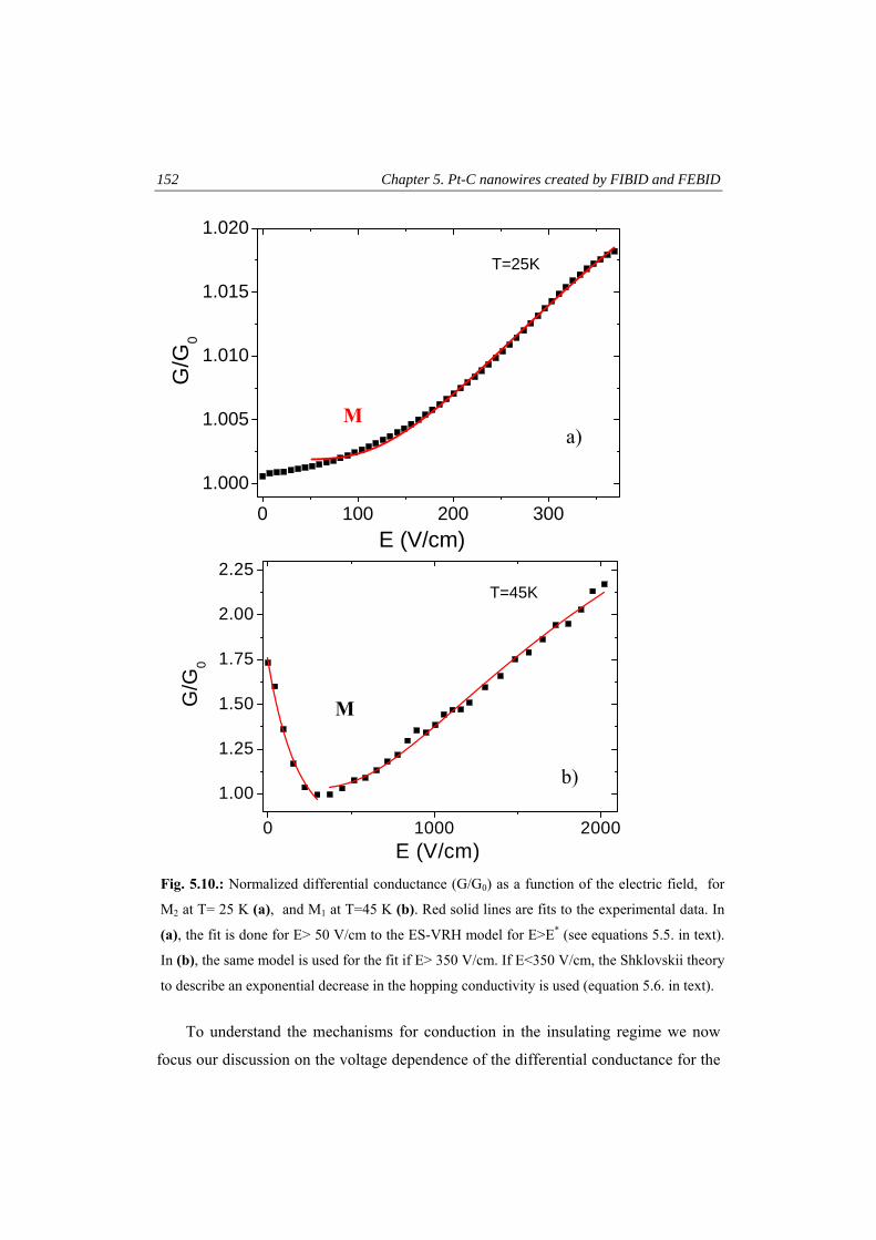
152 Chapter 5. Pt-C nanowires created by FIBID and FEBID
To understand the mechanisms for conduction in the insulating regime we now
focus our discussion on the voltage dependence of the differential conductance for the
0 100 200 3001.000
1.005
1.010
1.015
1.020
G/G
0
E (V/cm)
a) M
T=25K
0 1000 2000
1.00
1.25
1.50
1.75
2.00
2.25
E (V/cm)
G/G
0
b)
M
T=45K
Fig. 5.10.: Normalized differential conductance (G/G0) as a function of the electric field, for
M2 at T= 25 K (a), and M1 at T=45 K (b). Red solid lines are fits to the experimental data. In
(a), the fit is done for E> 50 V/cm to the ES-VRH model for E>E* (see equations 5.5. in text).
In (b), the same model is used for the fit if E> 350 V/cm. If E<350 V/cm, the Shklovskii theory
to describe an exponential decrease in the hopping conductivity is used (equation 5.6. in text).
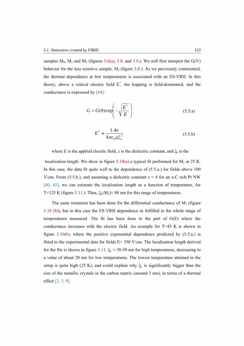
5.1. Nanowires created by FIBID 153
samples M0, M1 and M2 (figures 5.6(a), 5.8. and 5.9.). We will first interpret the G(V)
behavior for the less resistive sample, M2 (figure 5.8.). As we previously commented,
the thermal dependence at low temperatures is associated with an ES-VRH. In this
theory, above a critical electric field E*, the hopping is field-dominated, and the
conductance is expressed by [44]:
⎟⎟⎠
⎞⎜⎜⎝
⎛−=
EEGG
*
exp)0( (5.5.a)
20
*
44.1
L
eEεξπε
≈ (5.5.b)
where E is the applied electric field, ε is the dielectric constant, and ξL is the
localization length. We show in figure 5.10(a) a typical fit performed for M2 at 25 K.
In this case, the data fit quite well to the dependence of (5.5.a.) for fields above 100
V/cm. From (5.5.b.), and assuming a dielectric constant ε ≈ 4 for an a-C rich Pt NW
[40, 45], we can estimate the localization length as a function of temperature, for
T<125 K (figure 5.11.). Thus, ξL(M2)≈ 80 nm for this range of temperatures.
The same treatment has been done for the differential conductance of M1 (figure
5.10 (b)), but in this case the ES-VRH dependence in fulfilled in the whole range of
temperatures measured. The fit has been done to the part of G(E) where the
conductance increases with the electric field. An example for T=45 K is shown in
figure 5.10(b), where the positive exponential dependence predicted by (5.5.a.) is
fitted to the experimental data for fields E> 350 V/cm. The localization length derived
for the fits is shown in figure 5.11. ξL ≈ 30-50 nm for high temperatures, decreasing to
a value of about 20 nm for low temperatures. The lowest temperature attained in the
setup is quite high (25 K), and could explain why ξL is significantly bigger than the
size of the metallic crystals in the carbon matrix (around 3 nm), in terms of a thermal
effect [2, 3, 9].
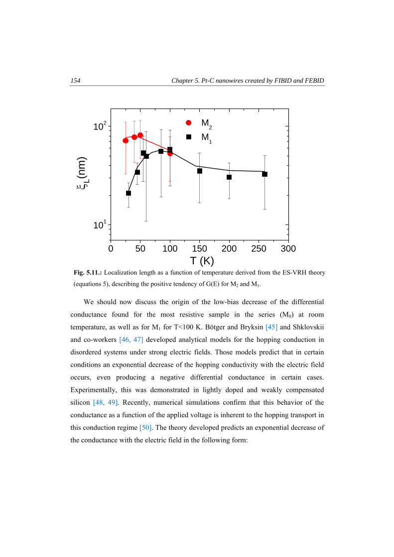
154 Chapter 5. Pt-C nanowires created by FIBID and FEBID
We should now discuss the origin of the low-bias decrease of the differential
conductance found for the most resistive sample in the series (M0) at room
temperature, as well as for M1 for T<100 K. Bötger and Bryksin [45] and Shklovskii
and co-workers [46, 47] developed analytical models for the hopping conduction in
disordered systems under strong electric fields. Those models predict that in certain
conditions an exponential decrease of the hopping conductivity with the electric field
occurs, even producing a negative differential conductance in certain cases.
Experimentally, this was demonstrated in lightly doped and weakly compensated
silicon [48, 49]. Recently, numerical simulations confirm that this behavior of the
conductance as a function of the applied voltage is inherent to the hopping transport in
this conduction regime [50]. The theory developed predicts an exponential decrease of
the conductance with the electric field in the following form:
Fig. 5.11.: Localization length as a function of temperature derived from the ES-VRH theory
(equations 5), describing the positive tendency of G(E) for M2 and M1.
0 50 100 150 200 250 300
101
102
ξ L(nm
)
T (K)
M2 M1
5.1. Nanowires created by FIBID 155
⎟⎠⎞
⎜⎝⎛ −
≈kT
eELGEG
2exp)0()( 0 (5.6.a)
88.0
074.1
3 ⎟⎟⎠
⎞⎜⎜⎝
⎛=
L
RRLξ
(5.6.b)
where R=N-1/3 is the mean inter-impurity distance, ξL is the localization length, and L0
is the typical length of the region where the electron gets “trapped”. This equation is
valid if eEL0>>kT. To understand the essence of the effect, let us think of a cluster
composed of impurities, responsible for the hopping conduction. In a hopping process
at moderate fields, the electron hops from one site to other, opposite to the electric
field. In this process, there exists the possibility that the electron arrives at a “dead-
end”, i.e. an impurity centre whose neighboring sites are distant enough to make it
energetically unfeasible that the electron to continue its way. If this happens, the
electron tries to move in the direction of the field to escape from this “trap” to further
continue hopping again opposite to E. However, if the conduction occurs under a
strong electric field, some of these backward movements are forbidden. Thus,
electrons get trapped in such dead–ends, and consequently the current density
decreases with E. For a detailed description of the phenomenon see references 45-47
and 50. We associate the decrease in G(V) found in M0 and M1 to this effect, in
complete agreement with the previous interpretations done for other ranges of
resistivities and fields. As observed experimentally in figures 5.6(a) and 5.9, after the
drop in G(V) at low bias, a change to positive slopes appears at even higher fields,
which is a direct consequence of the high value of the field, which provides enough
energy to overcome the traps in the system, resulting in the dependence of VRH with
field described by equation 5.6 [49].
We have used the equations (5.6.) to fit the experimental G(E) data of M0 and M1.
In figure 5.10 (b), the example for M1 at 45 K is shown, where the fit is done for
0<E<350 V/cm. For T>50 K, the criterion eEL0>>kT is not fulfilled, resulting in
unphysical values for L0 (≈ 10 µm), and consequently for the localization length
(below the nanometer). We therefore centre our study for T<50 K, where L0≈ 100 nm.
156 Chapter 5. Pt-C nanowires created by FIBID and FEBID
If we assume an impurity concentration similar to that which exists in silicon when the
exponential decrease in G(V) is observed, N≈ 1016 cm-3 [47, 49], an estimate of the ξL
can be made. For low temperatures, ξL ≈ 10 nm. This value approaches the one
estimated by the ES-VRH fits for the higher-bias increase of G(E), of around 20 nm.
The non-perfect agreement between both values seems logical, since assumptions
regarding the dielectric constant and the concentration of impurities are done in both
models. Nevertheless, the values are in the same order of magnitude, evidencing the
consistency of the analysis performed. If we apply the same procedure for M0 at room
temperature, we obtain L0 ≈ 200 nm, resulting in a localization length ξL ≈ 6 nm if an
impurity concentration N= 5 × 1015 cm-3 is assumed.
5.2. Comparison of NWs created by FEBID and FIBID 157
5.2. Comparison of NWs created by FEBID and FIBID
The aim of this section is to compare the electrical conduction properties of Pt-C
NWs grown by FEBID and by FIBID. The deposits are compared for thicknesses high
enough so that FIBID-NWs have metallic conduction (in the range of M4).
5.2.1. Experimental details
We detail the parameters different from those exposed in section 5.1.2.
5.2.1.1. Deposition parameters
The deposition parameters for FEBID-NWs are: (CH3)3Pt(CpCH3) precursor gas,
(TG) = 45 ºC precursor temperature, (VFEB) = 10 kV beam voltage, (IFEB) = 0.54 nA
beam current, substrate temperature = 22 ºC, dwell time = 1 µs, chamber base pressure
= 10-7 mbar, process pressure = 3 × 10⁻⁶ mbar, beam overlap = 0 %, distance between
GIS needle and substrate (LD) = 1.35 mm. For FIBID-NWs, the parameters are the
same as in section 5.1.2.1., except for TG = 45ºC, and LD=1.35 mm.
5.2.1.2. “In situ” electrical measurements
The procedure is identical to that described in section 5.1.2.2, except that the
resistance-versus-time measurements were done in a two-probe configuration, by
connecting the conductive microprobes via a feedthrough to a Keithley 2000
multimeter located out of the dual beam chamber, which allows measuring the deposit
resistance by two-probe measurements provided that its value is below 120 MΩ. A
constant current of value 700 nA was applied. The lead resistance, only about 13 Ω,
guarantees no significant influence on the measured resistance of the deposit, which is
at least two orders of magnitude larger as will be shown later.
5.2.1.3. High Resolution Transmission-Electron-Microscopy (HRTEM)
The high-resolution TEM (HRTEM) study was carried out using a Jeol 2010F
equipment operated at 200 kV (point to point resolution 0.19 nm) on Pt deposits
grown on Cu TEM grids with a supporting carbon membrane
158 Chapter 5. Pt-C nanowires created by FIBID and FEBID
5.2.2. Results
5.2.2.1. “In situ” measurements of the resistance as the NWs are grown
In figure 5.12 we compare Pt samples by FEBID and FIBID with similar
thickness in order to give evidence for the strong difference in the resistance of the
deposits. Three FEBID and FIBID deposits are shown to illustrate the reproducibility
of the results. In the case of FEBID (FIBID) deposits, after 6.3 (1.5) minutes, the
resistance reaches 120 MΩ and we start the resistance monitorization. After additional
deposition time of 14.6 (10.7) minutes, the final resistance is found to be 23.5 MΩ (1
kΩ). Even though the final thickness of all the deposits is roughly the same (∼160
nm), measured by conventional cross-section inspection, the resistance is four orders
of magnitude lower for FIBID-Pt than for FEBID-Pt. Thus, in the case of Pt by FEBID
the resistivity is about 107 µΩcm, whereas it is about 800 µΩcm cm in the case of Pt
by FIBID, in any case much higher than for bulk Pt, of 10.8 µΩcm. EDX analysis
reveals that a higher metallic/carbon content in the case of FIB-deposits is responsible
for the important differences in resistivity (In atomic percentage, FEBID-NWs:
C(%)=87.81 ± 0.21, Pt(%)=12.19 ± 0.2; FIBID NWs: C(%)=71.80 ± 0.22,
Pt(%)=17.40 ± 0.22, Ga(%)=10.80 ± 0.21).
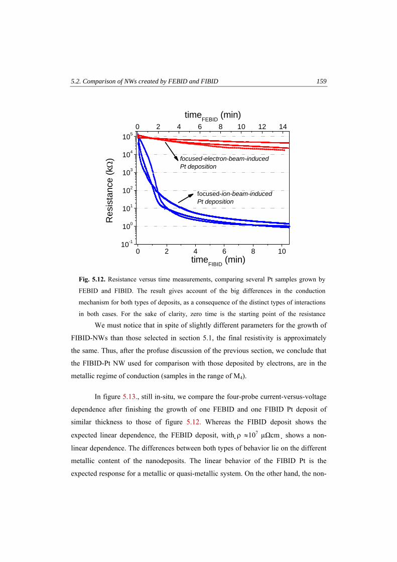
5.2. Comparison of NWs created by FEBID and FIBID 159
We must notice that in spite of slightly different parameters for the growth of
FIBID-NWs than those selected in section 5.1, the final resistivity is approximately
the same. Thus, after the profuse discussion of the previous section, we conclude that
the FIBID-Pt NW used for comparison with those deposited by electrons, are in the
metallic regime of conduction (samples in the range of M4).
In figure 5.13., still in-situ, we compare the four-probe current-versus-voltage
dependence after finishing the growth of one FEBID and one FIBID Pt deposit of
similar thickness to those of figure 5.12. Whereas the FIBID deposit shows the
expected linear dependence, the FEBID deposit, with ρ ≈107 µΩcm shows a non-
linear dependence. The differences between both types of behavior lie on the different
metallic content of the nanodeposits. The linear behavior of the FIBID Pt is the
expected response for a metallic or quasi-metallic system. On the other hand, the non-
0 2 4 6 8 1010-1
100
101
102
103
104
1050 2 4 6 8 10 12 14
timeFEBID (min)
focused-ion-beam-induced Pt deposition
Res
ista
nce
(kΩ
)
timeFIBID (min)
focused-electron-beam-induced Pt deposition
Fig. 5.12. Resistance versus time measurements, comparing several Pt samples grown by
FEBID and FIBID. The result gives account of the big differences in the conduction
mechanism for both types of deposits, as a consequence of the distinct types of interactions
in both cases. For the sake of clarity, zero time is the starting point of the resistance
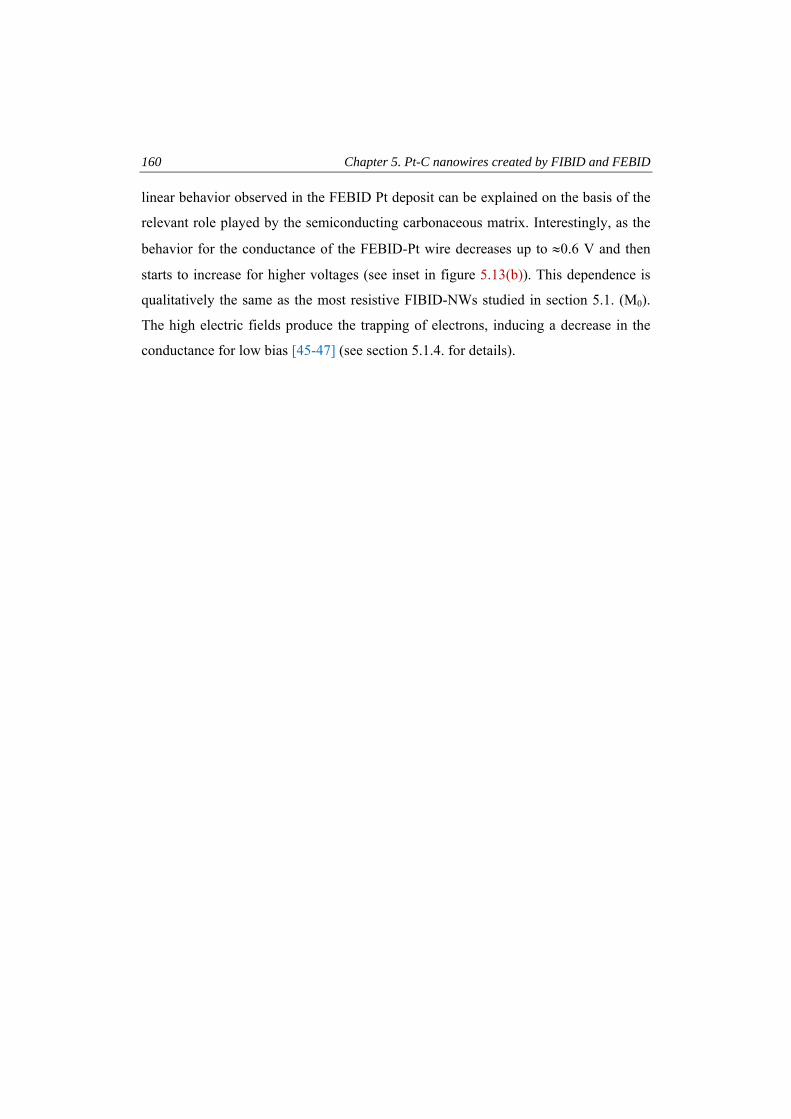
160 Chapter 5. Pt-C nanowires created by FIBID and FEBID
linear behavior observed in the FEBID Pt deposit can be explained on the basis of the
relevant role played by the semiconducting carbonaceous matrix. Interestingly, as the
behavior for the conductance of the FEBID-Pt wire decreases up to ≈0.6 V and then
starts to increase for higher voltages (see inset in figure 5.13(b)). This dependence is
qualitatively the same as the most resistive FIBID-NWs studied in section 5.1. (M0).
The high electric fields produce the trapping of electrons, inducing a decrease in the
conductance for low bias [45-47] (see section 5.1.4. for details).
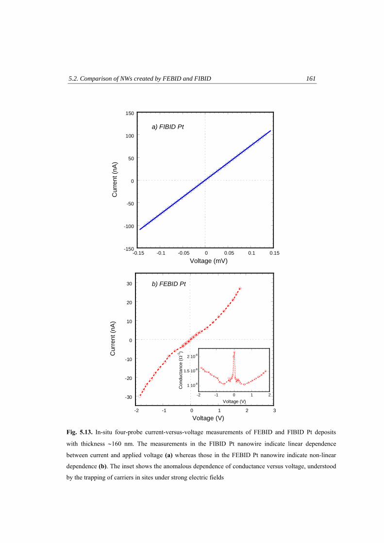
5.2. Comparison of NWs created by FEBID and FIBID 161
1 10-8
1.5 10-8
2 10-8
-2 -1 0 1 2
Con
duct
ance
(Ω
-1)
Voltage (V)-30
-20
-10
0
10
20
30
-2 -1 0 1 2 3
Cur
rent
(nA
)
Voltage (V)
b) FEBID Pt
300 K
-150
-100
-50
0
50
100
150
-0.15 -0.1 -0.05 0 0.05 0.1 0.15
Cur
rent
(nA
)
Voltage (mV)
a) FIBID Pt
300 K
Fig. 5.13. In-situ four-probe current-versus-voltage measurements of FEBID and FIBID Pt deposits
with thickness ∼160 nm. The measurements in the FIBID Pt nanowire indicate linear dependence
between current and applied voltage (a) whereas those in the FEBID Pt nanowire indicate non-linear
dependence (b). The inset shows the anomalous dependence of conductance versus voltage, understood
by the trapping of carriers in sites under strong electric fields
162 Chapter 5. Pt-C nanowires created by FIBID and FEBID
5.2.2.2. Temperature dependence of the electrical properties
In figure 5.14. the dependence of the resistance with temperature for the FEBID
deposit is shown (the behavior of the FIBID NW is almost negligible, as M4 in section
5.1.). R(T) shows a strong semiconductor behavior, and at T=150 K the resistance is
of the order of 1 GΩ, the maximum resistance that our experimental setup can
measure (a factor of 5.5 compared to 300 K). In the inset of figure 5.14., the
representation of ln(G) versus T-1/2 indicates that below 200 K the conduction
mechanism fits the ES-VRH [4] (equation 5.4., with N=0.5). The same temperature
-20
-19.5
-19
-18.5
-18
-17.5
-17
0.06 0.07 0.08
ln G
(ohm
s-1)
T (K) -1/2
280 K
160 K
VRH
200 K
5 107
1 108
1.5 108
2 108
2.5 108
3 108
160 180 200 220 240 260 280 300 320
Res
ista
nce
(Ω)
T (K)
b) FEBID Pt
Fig. 5.14. Temperature variation of the resistance of a FEBID Pt nanowire, showing a
semiconducting dependence. The inset shows the analysis of data in the form of ln(G)
versus T-1/2. An ES-VRH is deduced from this fit, for T >200 K
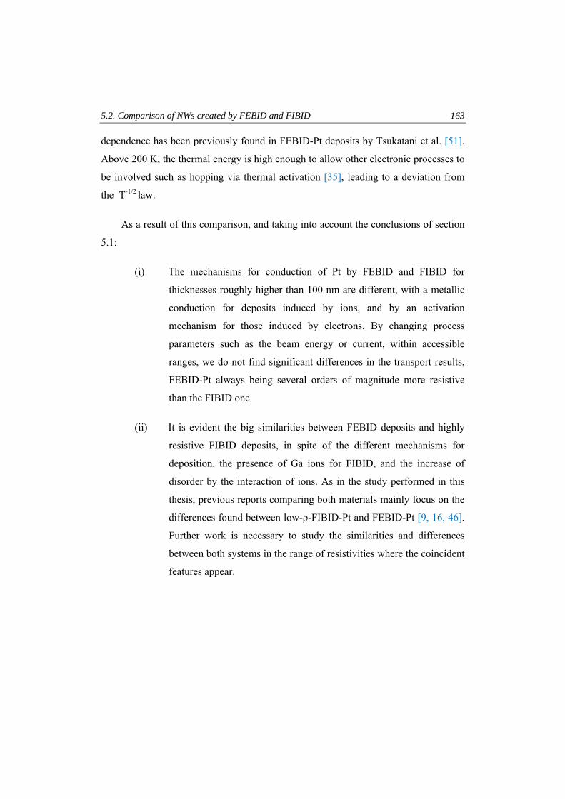
5.2. Comparison of NWs created by FEBID and FIBID 163
dependence has been previously found in FEBID-Pt deposits by Tsukatani et al. [51].
Above 200 K, the thermal energy is high enough to allow other electronic processes to
be involved such as hopping via thermal activation [35], leading to a deviation from
the T-1/2 law.
As a result of this comparison, and taking into account the conclusions of section
5.1:
(i) The mechanisms for conduction of Pt by FEBID and FIBID for
thicknesses roughly higher than 100 nm are different, with a metallic
conduction for deposits induced by ions, and by an activation
mechanism for those induced by electrons. By changing process
parameters such as the beam energy or current, within accessible
ranges, we do not find significant differences in the transport results,
FEBID-Pt always being several orders of magnitude more resistive
than the FIBID one
(ii) It is evident the big similarities between FEBID deposits and highly
resistive FIBID deposits, in spite of the different mechanisms for
deposition, the presence of Ga ions for FIBID, and the increase of
disorder by the interaction of ions. As in the study performed in this
thesis, previous reports comparing both materials mainly focus on the
differences found between low-ρ-FIBID-Pt and FEBID-Pt [9, 16, 46].
Further work is necessary to study the similarities and differences
between both systems in the range of resistivities where the coincident
features appear.
164 Chapter 5. Pt-C nanowires created by FIBID and FEBID
5.2.2.3. HRTEM images
For completeness, we include HRTEM images of both deposits [52] that illustrate
the reason for the different mechanisms of conduction.
As can be observed in figure 5.15., the FEBID and FIBID Pt-C wires consist of
ellipsoidal crystalline Pt grains embedded in an amorphous carbonaceous matrix. The
crystalline Pt grains are easily identified due to the clear observation of Pt atomic
b) FEBID Pt deposit
a) FIBID Pt deposit
(2 0 0)
(2 2 2)
(1 1 1)
(1 1 1)(2 0 0)
(2 0 2)
Fig. 5.15. HRTEM images of a Pt nanodeposit by FIBID (a) and FEBID (b), in both cases grown
at 30 kV beam energy on top of a TEM Cu grid covered with a thin supporting holey carbon
membrane. One Pt grain has been selected in each case for magnification and clear observation of
the corresponding atomic planes. The Fast-Fourier-Transform of the full image gives diffraction
spots that correspond to the (200), (111), (222) and (202) atomic planes of fcc Pt.
5.2. Comparison of NWs created by FEBID and FIBID 165
planes with the expected planar distances. Thus, fast-Fourier transforms of the images
give as a result the presence of diffraction spots corresponding to the planar distances
of 0.2263 nm, 0.1960 nm, 0.1386 nm, and 0.1132 nm, which correspond respectively
to the (111), (200), (202) and (222) atomic planes of fcc Pt, with lattice parameter of
0.3924 nm. An average size of Pt crystallites has been obtained from the measurement
of about 50 individual grains in each image through the counting of the number of
atomic planes. It is found that no matter the used beam energy and current, in all the
FEBID and FIBID deposits the average Pt crystallite size is about 3.2±0.8 nm. Thus,
from these HRTEM images, the microstructure of the FEBID and FIBID Pt deposits is
similar. The higher percentage of Pt in deposits by FIB brings about the percolation of
grains, inducing metallic characteristics in the electrical transport.
5.3. Conclusions
We have performed a detailed study of the transport properties of Pt-C NWs
grown by Focused-Ion/Electron-Beam induced deposition. By controlling the
resistance as the deposit is done, we can see the different regimes for the resistivity
existing in this material.
In the case of FIBID, we have deposited NWs with five different thicknesses, that
is, in five different regimes of (over 5 orders of magnitude) conductivity. By studying
NW resistivity as a function of temperature, as well as the dependence with voltage on
the differential conductivity, we observe a metal-insulator transition in the NWs as a
function of thickness (carbon-metal content). This transition is interpreted under the
theory of Mott-Anderson for non-metallic disordered materials. As the NW increases
in height, a higher concentration of metal is introduced in the semiconducting carbon
matrix. This gives rise to the appearance of impurity levels in the band gap, together
with the localization of states in the formed band tails. As the growth continues, the
introduction of metal clusters finally results in a delocalization of the electron wave-
functions, and NWs above 50 nm present metallic conduction.
This work explains the discrepancy existing for previous Pt-C nanostructures
created by FIB, where in some cases a metallic character was reported, in contrast to
others, where insulating conduction was observed. It also gives a counterpoint to the
traditional work when growing metal nanostructures by FIB, since we demonstrate the
possibility to deposit materials with different conduction characteristics, making it, in
principle, feasible to fabricate insulator or metal nanowires with the same technique
and precursor, just by controlling and changing the growth parameters. This is of
special relevance because of its potential extrapolation to other materials grown by
FIBID and FEBID, since most of the gas precursors used by these techniques use
organo-metallic gases, as it is the case here.
The comparison of metallic-FIBID and FEBID wires can be explained by the
different composition of both types of deposits, as a consequence of the different
mechanism responsible for deposition, with a lower metallic doping for deposits
induced by focused electrons. The common features between FEBID-NWs and low
5.3. Conclusions 167
metallic FIBID-NWs are also evidenced by electrical, spectroscopic and imaging
measurements.
The discovery of an exponential decrease in the differential conductance
behavior in low-metallic doped carbon NWs constitutes an experimental evidence in a
nanometric structure of the validity of the theories developed for hopping conduction
in strong fields. The existence of this trend in both types of deposits (grown by FEB
and FIB) indicates that this conduction process naturally appears in Pt-C NWs grown
with focused-beam methods.

Chapter 6
Superconductor W-based nanowires
created by FIBID
In this chapter the results obtained for W-based nanowires grown by Focused-Ion-
Beam-Induced-Deposition will be shown. This material is superconductor for
temperatures below ~5K
The first part of the chapter shows the characterization of the microstructure and
chemical composition, by High-Resolution-Transmission-Electron-Microscopy and X-
Ray Photoelectron Spectroscopy studies. The second part consists of the study of the
electrical measurements of wires, studying if the superconducting properties are
preserved for wire width in the nanoscale. Finally, and for completeness, spectacular
measurements by Scanning-Tunneling-Spectroscopy will be shown, as a result of
collaboration with the group of Prof. Vieira and Dr. Suderow (UAM, Madrid).
170 Chapter 6. Superconductor W-based nanowires created by FIBID
6.1. Introduction
6.1.1. Nanoscale superconductors
Since the discovery of the superconductivity in 1911 by Kamerling Onnes [1],
superconductor materials (SCs) have been one of the main research subjects in
condensed-matter physics over the last 100 years. As a result, lots of important
findings have been done, with the Fe-based SCs [2] as maybe the last hottest topic in
the field. As important applications of SCs, we could cite, among others, the
production of high magnetic field coils, applied in Magnetic Resonance Imaging, or
SQUID magnetometers. Nowadays, large effort is being made in the search of better
SC properties, by finding new materials, or by the modification of existing ones, as
well as their behavior at the nanoscale. Basic studies regarding one-dimensional
superconductivity [3], vortex confinement [4, 5], vortex pinning [6], etc. have been
tackled recently. The fabrication of nanoSQUIDS is one of the most appealing
applications of such nano-superconductors [7, 8] as well as being supporting material
for superconducting quantum bits [9, 10]. As in other branches of Nanoscience based
on a top-down approximation, complex nanolithography techniques such as electron-
beam lithography, involving several process steps, are used to create such
superconducting nanostructures.
6.1.2. Previous results in FIBID-W
Sadki et al [11] discovered in 2004 that W-based nanodeposits created by 30kV-
FIBID, using W(CO)6 as gas precursor, were superconductors, with a critical
temperature around 5 K, substantially higher than in metallic crystalline W ( Tc = 0.01
K) [12]. This high Tc was associated to the amorphous character of the material, as
determined by X-Ray diffraction measurements, as well as by the presence of C and
Ga inside the deposits (in atomic percentage, determined by EDX: W/C/Ga
=40/40/20%). Values for the critical field (Bc2=9.5 T) and current density (Jc= 0.15
MA/cm2) were deduced from electrical measurements in wires of 10 µm (length) ×
300 nm (width) × 120 nm (thickness).
6.1. Introduction 171
A few more results can be found in the literature after this important result. The
most relevant references are:
(i) Luxmoore et al [13]: analogous W-based deposits by electrons
(FEBID) do not present SC transition down to 1.6 K, suggesting the
importance of Ga in the SC properties in FIBID-W, by getting
implanted and creating amorphization.
(ii) Spodding et al [14]: Measurement of resistance during the growth of
500 nm-wide W-C wires, and study of Bc2 and Jc, with similar results
to those of reference 11.
(iii) Li et al [15]: It is claimed that Tc can be tuned from 5.0 to 6.2 K by
varying the FIB current. This is explained by the modulation of
disorder created by ions near the metal-insulator transition, in
accordance with the theory developed by Osofsky et al [16].
(iv) Kasumov et al [17, 18]: An interesting application of these W-
nanodeposits is its use as resistance-free leads, for the electrical
characterization of contacted single organometallic molecules.
172 Chapter 6. Superconductor W-based nanowires created by FIBID
6.2. Experimental details
The FIBID superconducting nanodeposits were fabricated at room temperature in
the dual-beam equipment detailed in section 2., which uses a 5-30 kV Ga+ FIB. The
W(CO)6 precursor gas is brought onto the substrate surface by a GIS, where it
becomes decomposed by the FIB. Common parameters for this deposition process are:
Precursor gas temperature=50 ºC, Vol/dose=8.3 × 10-2 µm3/nC, dwell time=200 ns,
beam overlap= 0%, chamber base pressure = 10-7 mbar, process pressure = 6 × 10⁻⁶
mbar, distance between GIS needle and substrate = 150 µm.
6.2.1. HRTEM analysis
The high-resolution transmission electron microscopy (HRTEM) study was
carried out using a FEG-TEM Jeol 1010 equipment operated at 200 kV (point to point
resolution 0.19 nm) on 20 nm-thick W nanodeposits directly grown on TEM grids for
electron transparency in the experiment.
6.2.2. XPS measurements
A 100µm ×100µm ×100 nm sample was deposited on a Si wafer, using VBEAM=
30 kV, IBEAM =5 nA.
The measurements were done in the equipment detailed in chapter 2. A 5kV-
argon etching, with current densities of the order of 0.15A/m2 was done, to obtain a
depth profile of the deposits (probing every 20nm). For the quantitative analysis of the
XPS spectra, we used pseudo-Voigt peak profiles with a 10 to 20% Lorentzian
contribution, subtracting a Shirley -type background.
6.2.3. Electrical measurement in rectangular (micro- and nano-) wires
Rectangular wires were deposited on previously-micropatterned SiO2//Si, where
Al or Ti pads were evaporated after an optical lithography process, to realize contact
pads for the magnetotransport measurements (see details of lithography in section 2).
The dimensions of the wires are: length=12 µm, variable width and thickness (2
types). The first type consists of microwires (Mi) with width ≈ 2 µm and thickness ≈ 1

6.2. Experimental details 173
µm, and the second type consists of nanowires (Ni) with widths in the range 100-250
nm and thickness of 100-150 nm. The different parameters used are detailed in table
6.I.
The transport measurements (up to 9 T magnetic fields) were done in a PPMS
system (Quantum Design).
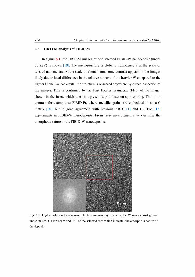
174 Chapter 6. Superconductor W-based nanowires created by FIBID
6.3. HRTEM analysis of FIBID-W
In figure 6.1. the HRTEM images of one selected FIBID-W nanodeposit (under
30 keV) is shown [19]. The microstructure is globally homogeneous at the scale of
tens of nanometers. At the scale of about 1 nm, some contrast appears in the images
likely due to local differences in the relative amount of the heavier W compared to the
lighter C and Ga. No crystalline structure is observed anywhere by direct inspection of
the images. This is confirmed by the Fast Fourier Transform (FFT) of the image,
shown in the inset, which does not present any diffraction spot or ring. This is in
contrast for example to FIBID-Pt, where metallic grains are embedded in an a-C
matrix [20], but in good agreement with previous XRD [11] and HRTEM [13]
experiments in FIBID-W nanodeposits. From these measurements we can infer the
amorphous nature of the FIBID-W nanodeposits.
5 nm
Fig. 6.1. High-resolution transmission electron microscopy image of the W nanodeposit grown
under 30 keV Ga-ion beam and FFT of the selected area which indicates the amorphous nature of
the deposit.
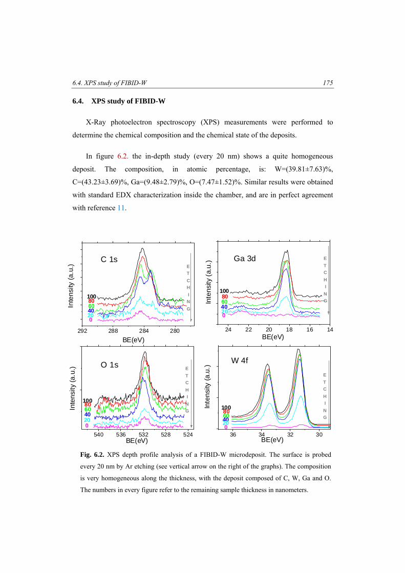
6.4. XPS study of FIBID-W 175
6.4. XPS study of FIBID-W
X-Ray photoelectron spectroscopy (XPS) measurements were performed to
determine the chemical composition and the chemical state of the deposits.
In figure 6.2. the in-depth study (every 20 nm) shows a quite homogeneous
deposit. The composition, in atomic percentage, is: W=(39.81±7.63)%,
C=(43.23±3.69)%, Ga=(9.48±2.79)%, O=(7.47±1.52)%. Similar results were obtained
with standard EDX characterization inside the chamber, and are in perfect agreement
with reference 11.
Fig. 6.2. XPS depth profile analysis of a FIBID-W microdeposit. The surface is probed
every 20 nm by Ar etching (see vertical arrow on the right of the graphs). The composition
is very homogeneous along the thickness, with the deposit composed of C, W, Ga and O.
The numbers in every figure refer to the remaining sample thickness in nanometers.
24 22 20 18 16 14
Inte
nsity
(a.u
.) Ga 3d
BE(eV)
ETCH ING
100806040200
292 288 284 280
100
200
300
400
500
600
In
tens
ity (a
.u.)
BE(eV)
ETCH ING
100806040200
C 1s
540 536 532 528 524
300
400
In
tens
ity (a
.u.)
BE(eV)
O 1s ETCH ING
100806040200
36 34 32 30
W 4f
Inte
nsity
(a.u
.)
BE(eV)
ETCH ING
100806040200
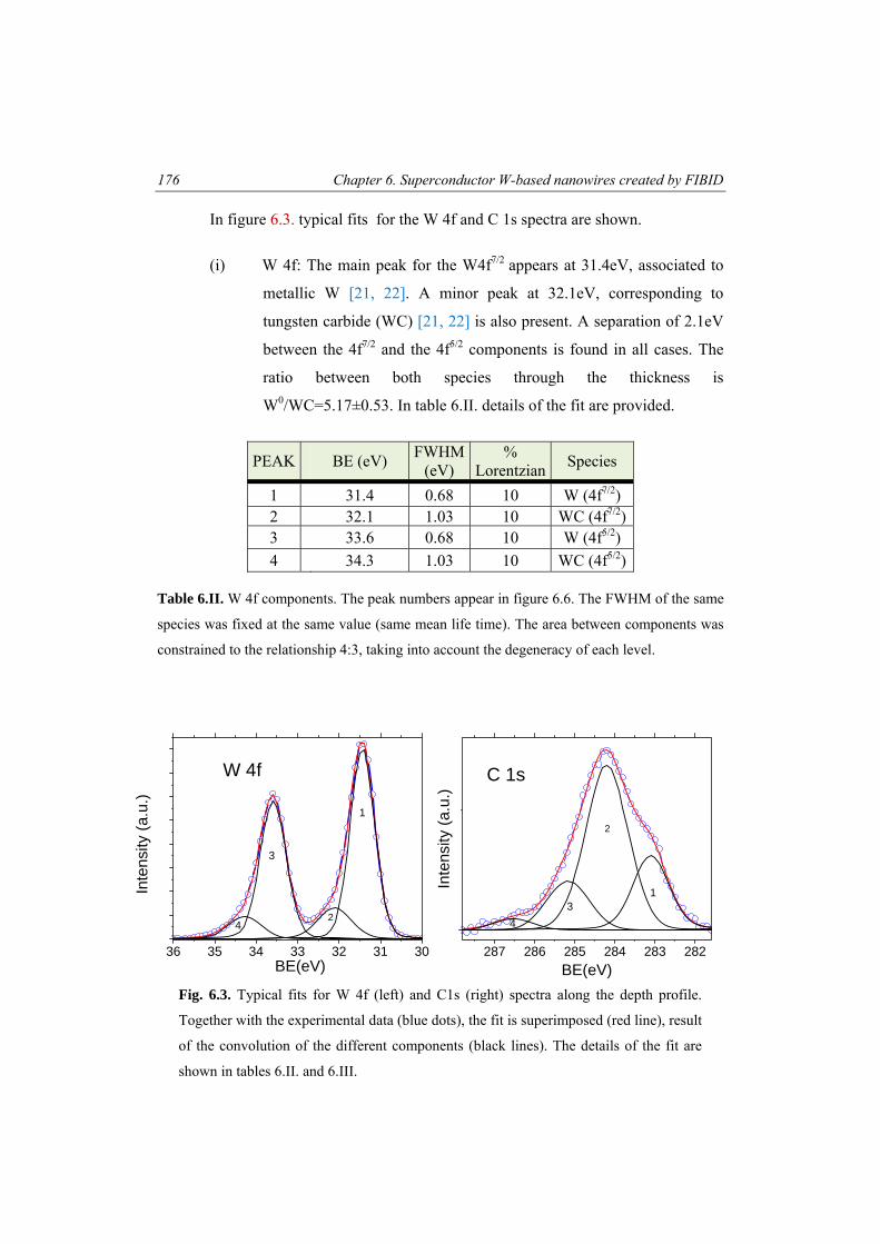
176 Chapter 6. Superconductor W-based nanowires created by FIBID
In figure 6.3. typical fits for the W 4f and C 1s spectra are shown.
(i) W 4f: The main peak for the W4f7/2 appears at 31.4eV, associated to
metallic W [21, 22]. A minor peak at 32.1eV, corresponding to
tungsten carbide (WC) [21, 22] is also present. A separation of 2.1eV
between the 4f7/2 and the 4f5/2 components is found in all cases. The
ratio between both species through the thickness is
W0/WC=5.17±0.53. In table 6.II. details of the fit are provided.
PEAK BE (eV) FWHM (eV)
% Lorentzian Species
1 31.4 0.68 10 W (4f7/2) 2 32.1 1.03 10 WC (4f7/2) 3 33.6 0.68 10 W (4f5/2) 4 34.3 1.03 10 WC (4f5/2)
Table 6.II. W 4f components. The peak numbers appear in figure 6.6. The FWHM of the same
species was fixed at the same value (same mean life time). The area between components was
constrained to the relationship 4:3, taking into account the degeneracy of each level.
36 35 34 33 32 31 300
200
400
600
800
1000
1200
1400
1600
W 4f
Ratio(W/WC) ∼ 4.5 - 5
Inte
nsity
(a.u
.)
BE(eV)
4
3
2
1
287 286 285 284 283 282
0
C 1s
43
2
Inte
nsity
(a.u
.)
BE(eV)
1
Fig. 6.3. Typical fits for W 4f (left) and C1s (right) spectra along the depth profile.
Together with the experimental data (blue dots), the fit is superimposed (red line), result
of the convolution of the different components (black lines). The details of the fit are
shown in tables 6.II. and 6.III.
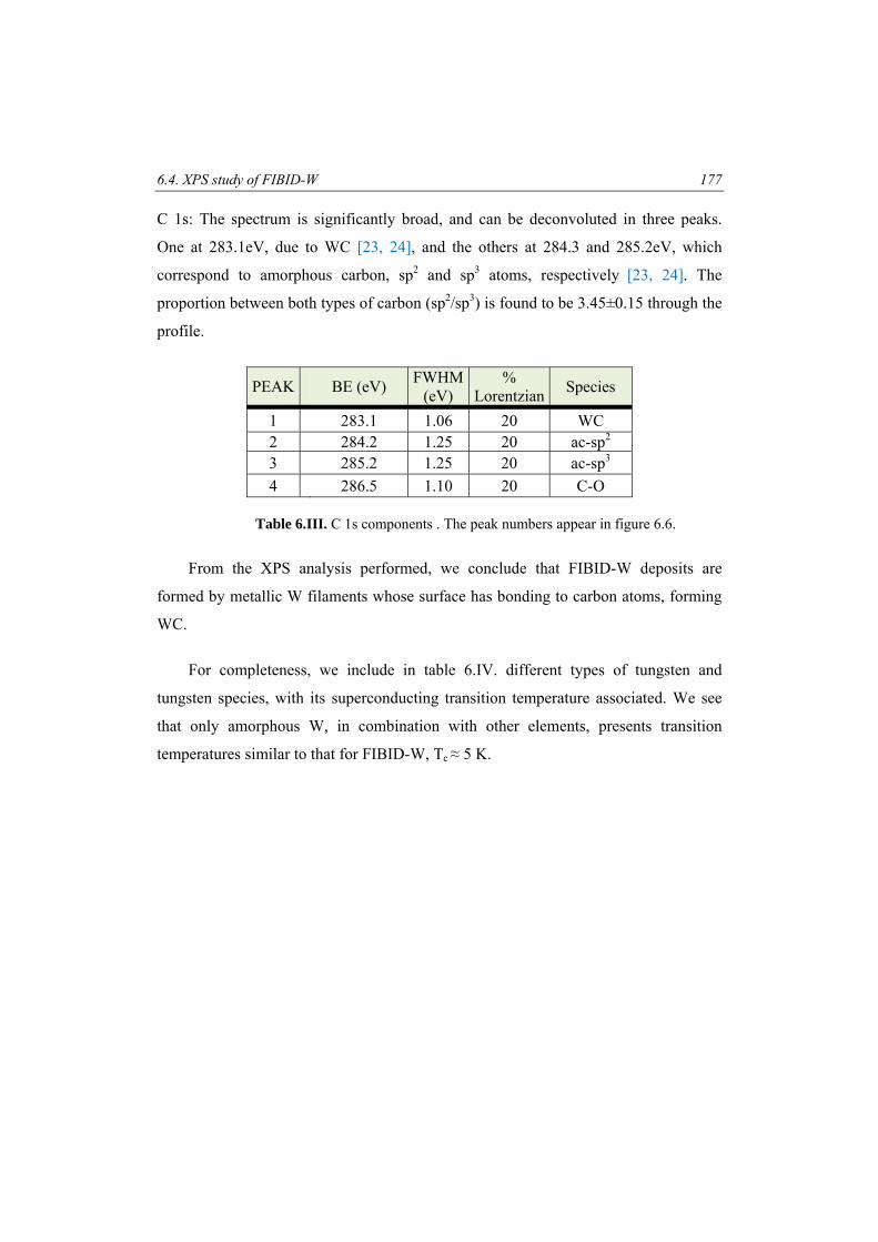
6.4. XPS study of FIBID-W 177
C 1s: The spectrum is significantly broad, and can be deconvoluted in three peaks.
One at 283.1eV, due to WC [23, 24], and the others at 284.3 and 285.2eV, which
correspond to amorphous carbon, sp2 and sp3 atoms, respectively [23, 24]. The
proportion between both types of carbon (sp2/sp3) is found to be 3.45±0.15 through the
profile.
PEAK BE (eV) FWHM (eV)
% Lorentzian Species
1 283.1 1.06 20 WC 2 284.2 1.25 20 ac-sp2 3 285.2 1.25 20 ac-sp3 4 286.5 1.10 20 C-O
Table 6.III. C 1s components . The peak numbers appear in figure 6.6.
From the XPS analysis performed, we conclude that FIBID-W deposits are
formed by metallic W filaments whose surface has bonding to carbon atoms, forming
WC.
For completeness, we include in table 6.IV. different types of tungsten and
tungsten species, with its superconducting transition temperature associated. We see
that only amorphous W, in combination with other elements, presents transition
temperatures similar to that for FIBID-W, Tc ≈ 5 K.
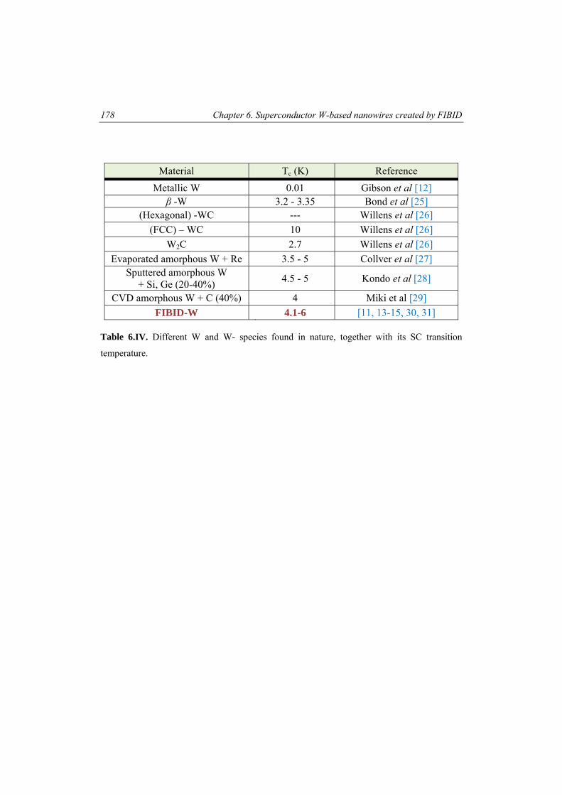
178 Chapter 6. Superconductor W-based nanowires created by FIBID
Material Tc (K) Reference Metallic W 0.01 Gibson et al [12] β -W 3.2 - 3.35 Bond et al [25]
(Hexagonal) -WC --- Willens et al [26] (FCC) – WC 10 Willens et al [26]
W2C 2.7 Willens et al [26] Evaporated amorphous W + Re 3.5 - 5 Collver et al [27]
Sputtered amorphous W + Si, Ge (20-40%) 4.5 - 5 Kondo et al [28]
CVD amorphous W + C (40%) 4 Miki et al [29] FIBID-W 4.1-6 [11, 13-15, 30, 31]
Table 6.IV. Different W and W- species found in nature, together with its SC transition
temperature.
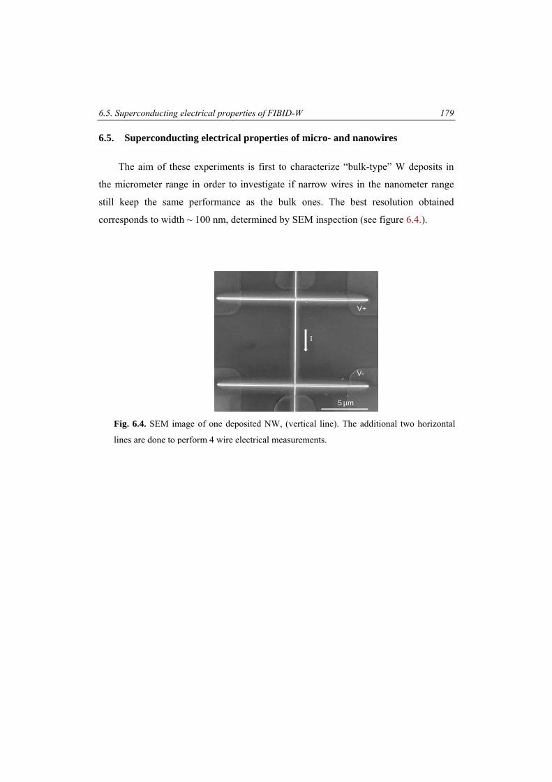
6.5. Superconducting electrical properties of FIBID-W 179
6.5. Superconducting electrical properties of micro- and nanowires
The aim of these experiments is first to characterize “bulk-type” W deposits in
the micrometer range in order to investigate if narrow wires in the nanometer range
still keep the same performance as the bulk ones. The best resolution obtained
corresponds to width ~ 100 nm, determined by SEM inspection (see figure 6.4.).
Fig. 6.4. SEM image of one deposited NW, (vertical line). The additional two horizontal
lines are done to perform 4 wire electrical measurements.
V+
V-
5 µm
I
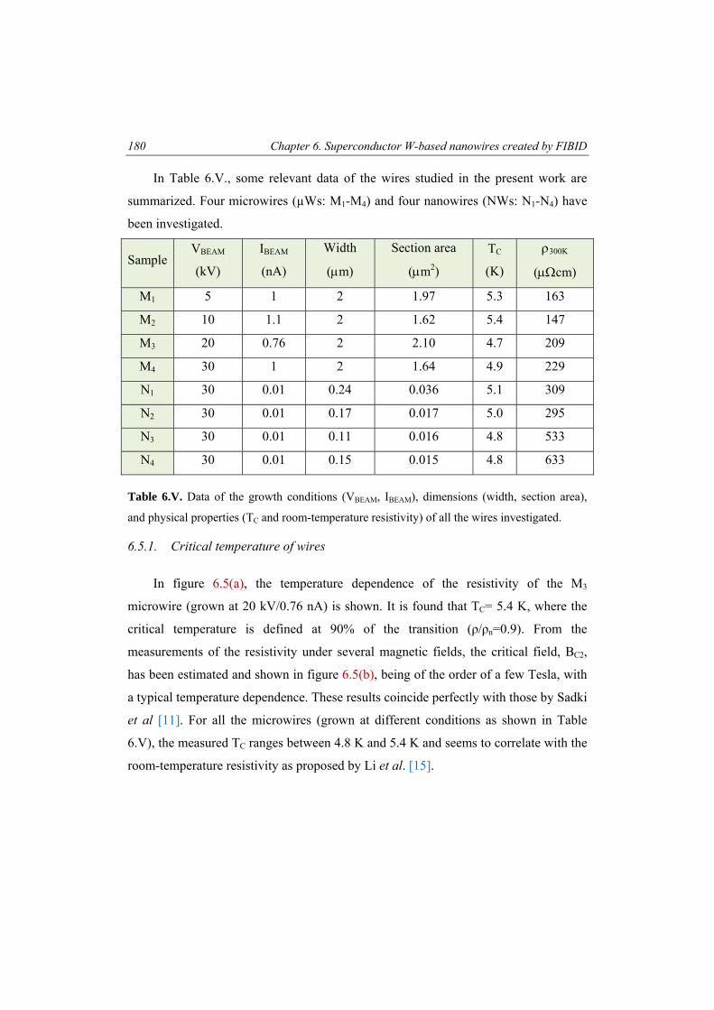
180 Chapter 6. Superconductor W-based nanowires created by FIBID
In Table 6.V., some relevant data of the wires studied in the present work are
summarized. Four microwires (µWs: M1-M4) and four nanowires (NWs: N1-N4) have
been investigated.
Sample VBEAM
(kV)
IBEAM
(nA)
Width
(μm)
Section area
(μm2)
TC
(K)
ρ300K
(μΩcm)
M1 5 1 2 1.97 5.3 163
M2 10 1.1 2 1.62 5.4 147
M3 20 0.76 2 2.10 4.7 209
M4 30 1 2 1.64 4.9 229
N1 30 0.01 0.24 0.036 5.1 309
N2 30 0.01 0.17 0.017 5.0 295
N3 30 0.01 0.11 0.016 4.8 533
N4 30 0.01 0.15 0.015 4.8 633
Table 6.V. Data of the growth conditions (VBEAM, IBEAM), dimensions (width, section area),
and physical properties (TC and room-temperature resistivity) of all the wires investigated.
6.5.1. Critical temperature of wires
In figure 6.5(a), the temperature dependence of the resistivity of the M3
microwire (grown at 20 kV/0.76 nA) is shown. It is found that TC= 5.4 K, where the
critical temperature is defined at 90% of the transition (ρ/ρn=0.9). From the
measurements of the resistivity under several magnetic fields, the critical field, BC2,
has been estimated and shown in figure 6.5(b), being of the order of a few Tesla, with
a typical temperature dependence. These results coincide perfectly with those by Sadki
et al [11]. For all the microwires (grown at different conditions as shown in Table
6.V), the measured TC ranges between 4.8 K and 5.4 K and seems to correlate with the
room-temperature resistivity as proposed by Li et al. [15].
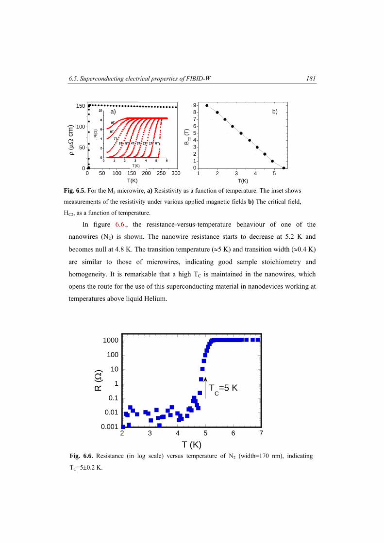
6.5. Superconducting electrical properties of FIBID-W 181
In figure 6.6., the resistance-versus-temperature behaviour of one of the
nanowires (N2) is shown. The nanowire resistance starts to decrease at 5.2 K and
becomes null at 4.8 K. The transition temperature (≈5 K) and transition width (≈0.4 K)
are similar to those of microwires, indicating good sample stoichiometry and
homogeneity. It is remarkable that a high TC is maintained in the nanowires, which
opens the route for the use of this superconducting material in nanodevices working at
temperatures above liquid Helium.
Fig. 6.5. For the M3 microwire, a) Resistivity as a function of temperature. The inset shows
measurements of the resistivity under various applied magnetic fields b) The critical field,
HC2, as a function of temperature.
0 50 100 150 200 250 3000
50
100
150
ρ (μ
Ω c
m)
T(K)
0 1 2 3 4 5 60
2
4
6
8
10
R(o
hm)
T (K)
0T1T2T3T4T5T6T7T
8T
9T
T(K)
R(Ω
)
0 1 2 3 4 5 60
2
4
6
8
10
R(o
hm)
T (K)
0T1T2T3T4T5T6T7T
8T
9T
T(K)
R(Ω
)
1 2 3 4 50123456789
BC
2 (T)
T(K)
a) b)
0.001
0.01
0.1
1
10
100
1000
2 3 4 5 6 7
R (Ω
)
T (K)
TC=5 K
Fig. 6.6. Resistance (in log scale) versus temperature of N2 (width=170 nm), indicating
TC=5±0.2 K.
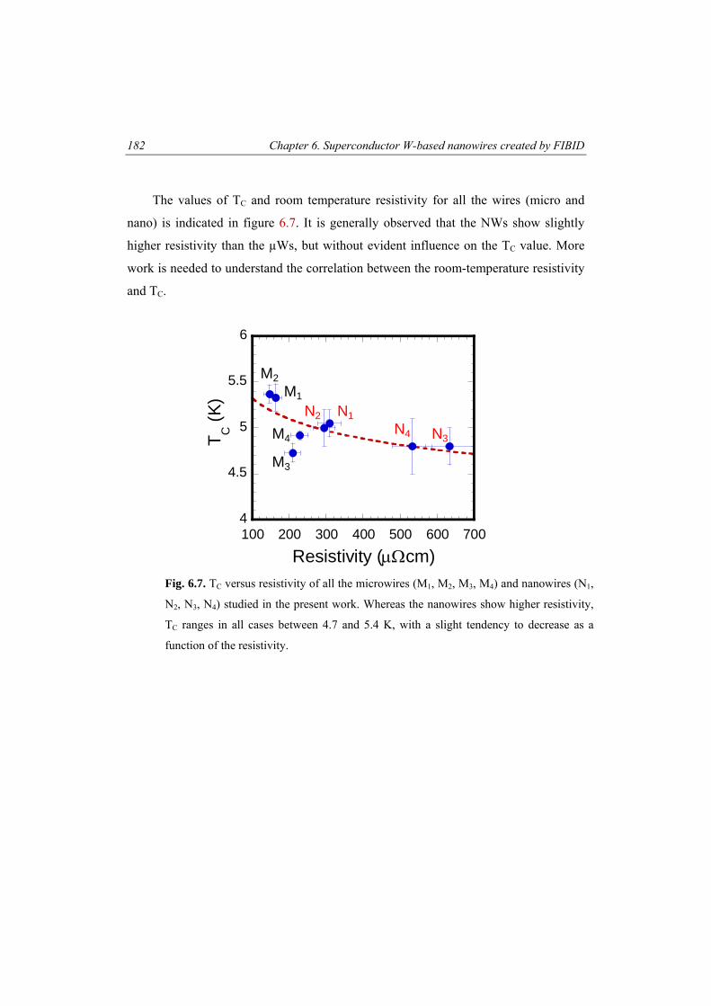
182 Chapter 6. Superconductor W-based nanowires created by FIBID
The values of TC and room temperature resistivity for all the wires (micro and
nano) is indicated in figure 6.7. It is generally observed that the NWs show slightly
higher resistivity than the µWs, but without evident influence on the TC value. More
work is needed to understand the correlation between the room-temperature resistivity
and TC.
4
4.5
5
5.5
6
100 200 300 400 500 600 700
T C (K
)
Resistivity (μΩcm)
M2M1
M4
M3
N2 N1N4 N3
Fig. 6.7. TC versus resistivity of all the microwires (M1, M2, M3, M4) and nanowires (N1,
N2, N3, N4) studied in the present work. Whereas the nanowires show higher resistivity,
TC ranges in all cases between 4.7 and 5.4 K, with a slight tendency to decrease as a
function of the resistivity.
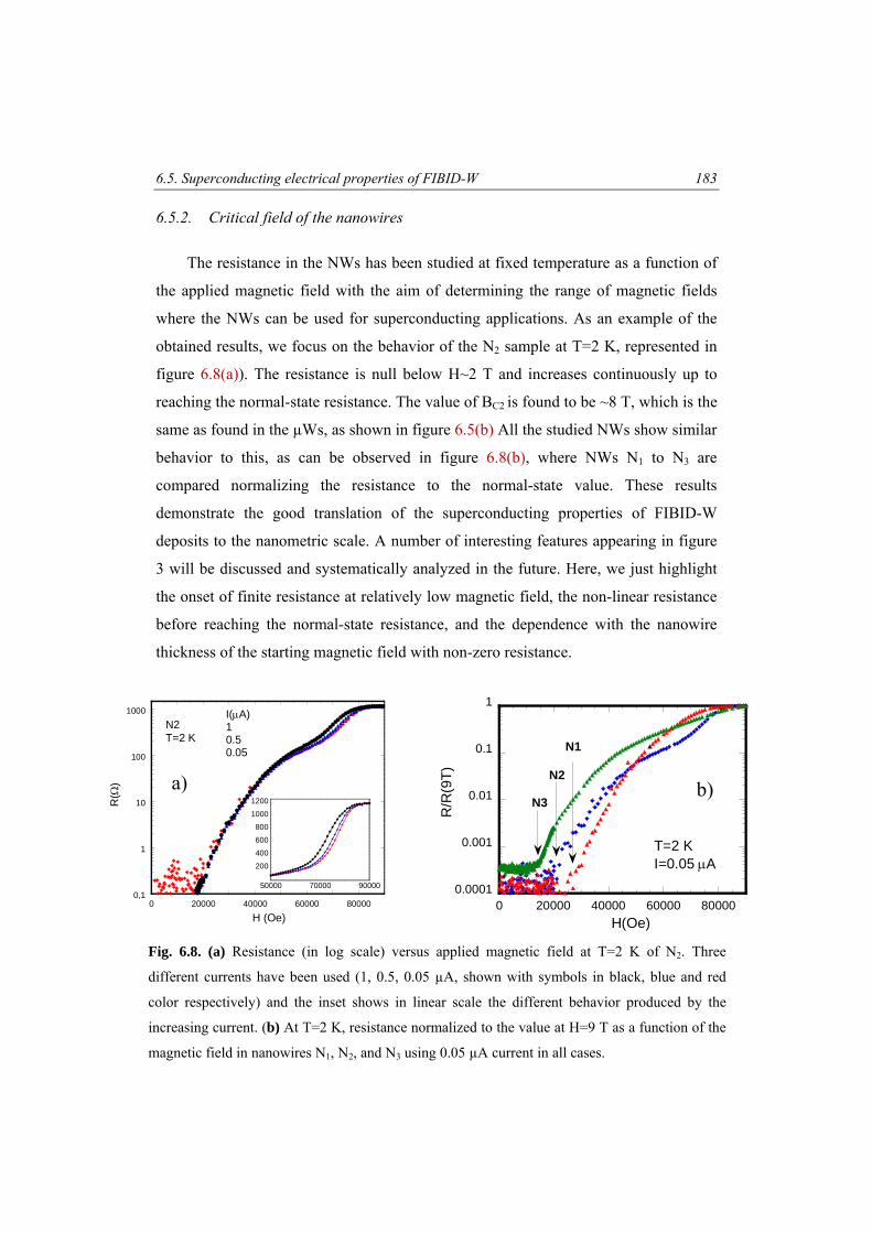
6.5. Superconducting electrical properties of FIBID-W 183
6.5.2. Critical field of the nanowires
The resistance in the NWs has been studied at fixed temperature as a function of
the applied magnetic field with the aim of determining the range of magnetic fields
where the NWs can be used for superconducting applications. As an example of the
obtained results, we focus on the behavior of the N2 sample at T=2 K, represented in
figure 6.8(a)). The resistance is null below H~2 T and increases continuously up to
reaching the normal-state resistance. The value of BC2 is found to be ~8 T, which is the
same as found in the µWs, as shown in figure 6.5(b) All the studied NWs show similar
behavior to this, as can be observed in figure 6.8(b), where NWs N1 to N3 are
compared normalizing the resistance to the normal-state value. These results
demonstrate the good translation of the superconducting properties of FIBID-W
deposits to the nanometric scale. A number of interesting features appearing in figure
3 will be discussed and systematically analyzed in the future. Here, we just highlight
the onset of finite resistance at relatively low magnetic field, the non-linear resistance
before reaching the normal-state resistance, and the dependence with the nanowire
thickness of the starting magnetic field with non-zero resistance.
Fig. 6.8. (a) Resistance (in log scale) versus applied magnetic field at T=2 K of N2. Three
different currents have been used (1, 0.5, 0.05 µA, shown with symbols in black, blue and red
color respectively) and the inset shows in linear scale the different behavior produced by the
increasing current. (b) At T=2 K, resistance normalized to the value at H=9 T as a function of the
magnetic field in nanowires N1, N2, and N3 using 0.05 µA current in all cases.
0,1
1
10
100
1000
0 20000 40000 60000 80000
R(Ω
)
H (Oe)
N2T=2 K
I(μA)10.50.05
200
400
600
8001000
1200
50000 70000 90000 0.0001
0.001
0.01
0.1
1
0 20000 40000 60000 80000
R/R
(9T)
H(Oe)
N1
N2
N3
T=2 KI=0.05 μA
0,1
1
10
100
1000
0 20000 40000 60000 80000
R(Ω
)
H (Oe)
N2T=2 K
I(μA)10.50.05
200
400
600
8001000
1200
50000 70000 90000 0.0001
0.001
0.01
0.1
1
0 20000 40000 60000 80000
R/R
(9T)
H(Oe)
N1
N2
N3
T=2 KI=0.05 μA
a) b)
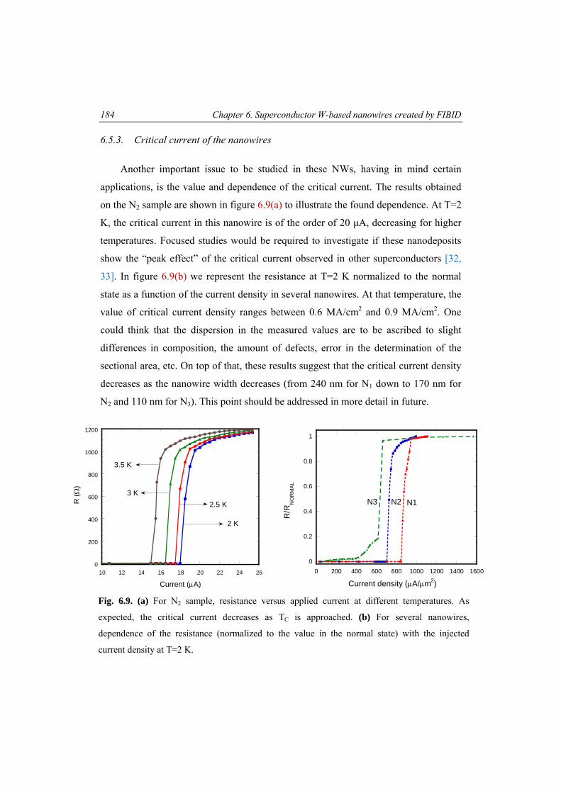
184 Chapter 6. Superconductor W-based nanowires created by FIBID
6.5.3. Critical current of the nanowires
Another important issue to be studied in these NWs, having in mind certain
applications, is the value and dependence of the critical current. The results obtained
on the N2 sample are shown in figure 6.9(a) to illustrate the found dependence. At T=2
K, the critical current in this nanowire is of the order of 20 μA, decreasing for higher
temperatures. Focused studies would be required to investigate if these nanodeposits
show the “peak effect” of the critical current observed in other superconductors [32,
33]. In figure 6.9(b) we represent the resistance at T=2 K normalized to the normal
state as a function of the current density in several nanowires. At that temperature, the
value of critical current density ranges between 0.6 MA/cm2 and 0.9 MA/cm2. One
could think that the dispersion in the measured values are to be ascribed to slight
differences in composition, the amount of defects, error in the determination of the
sectional area, etc. On top of that, these results suggest that the critical current density
decreases as the nanowire width decreases (from 240 nm for N1 down to 170 nm for
N2 and 110 nm for N3). This point should be addressed in more detail in future.
0
200
400
600
800
1000
1200
10 12 14 16 18 20 22 24 26
R (Ω
)
Current (μA)
2 K
3.5 K
3 K2.5 K
0
0.2
0.4
0.6
0.8
1
0 200 400 600 800 1000 1200 1400 1600
R/R
NO
RM
AL
Current density (μA/μm2)
N1N2N3
0
200
400
600
800
1000
1200
10 12 14 16 18 20 22 24 26
R (Ω
)
Current (μA)
2 K
3.5 K
3 K2.5 K
0
0.2
0.4
0.6
0.8
1
0 200 400 600 800 1000 1200 1400 1600
R/R
NO
RM
AL
Current density (μA/μm2)
N1N2N3
Fig. 6.9. (a) For N2 sample, resistance versus applied current at different temperatures. As
expected, the critical current decreases as TC is approached. (b) For several nanowires,
dependence of the resistance (normalized to the value in the normal state) with the injected
current density at T=2 K.
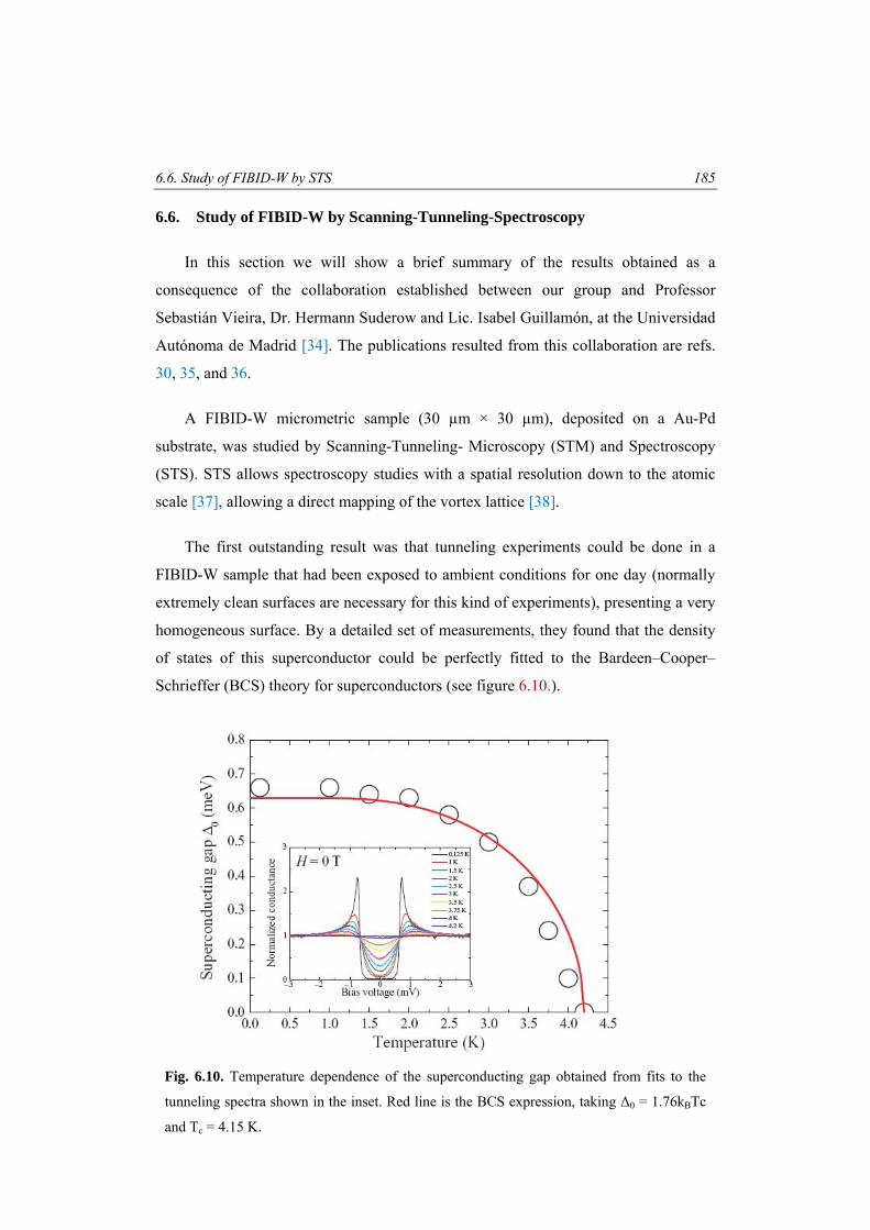
6.6. Study of FIBID-W by STS 185
6.6. Study of FIBID-W by Scanning-Tunneling-Spectroscopy
In this section we will show a brief summary of the results obtained as a
consequence of the collaboration established between our group and Professor
Sebastián Vieira, Dr. Hermann Suderow and Lic. Isabel Guillamón, at the Universidad
Autónoma de Madrid [34]. The publications resulted from this collaboration are refs.
30, 35, and 36.
A FIBID-W micrometric sample (30 µm × 30 µm), deposited on a Au-Pd
substrate, was studied by Scanning-Tunneling- Microscopy (STM) and Spectroscopy
(STS). STS allows spectroscopy studies with a spatial resolution down to the atomic
scale [37], allowing a direct mapping of the vortex lattice [38].
The first outstanding result was that tunneling experiments could be done in a
FIBID-W sample that had been exposed to ambient conditions for one day (normally
extremely clean surfaces are necessary for this kind of experiments), presenting a very
homogeneous surface. By a detailed set of measurements, they found that the density
of states of this superconductor could be perfectly fitted to the Bardeen–Cooper–
Schrieffer (BCS) theory for superconductors (see figure 6.10.).
Fig. 6.10. Temperature dependence of the superconducting gap obtained from fits to the
tunneling spectra shown in the inset. Red line is the BCS expression, taking Δ0 = 1.76kBTc
and Tc = 4.15 K.
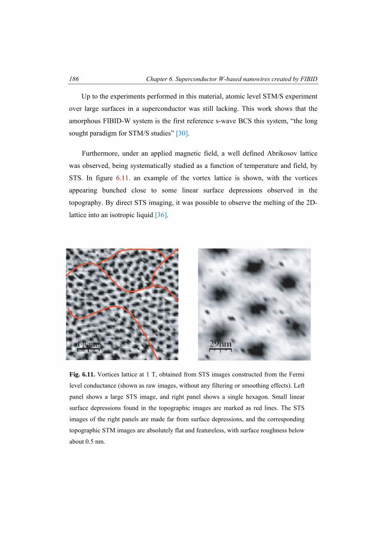
186 Chapter 6. Superconductor W-based nanowires created by FIBID
Up to the experiments performed in this material, atomic level STM/S experiment
over large surfaces in a superconductor was still lacking. This work shows that the
amorphous FIBID-W system is the first reference s-wave BCS this system, “the long
sought paradigm for STM/S studies” [30].
Furthermore, under an applied magnetic field, a well defined Abrikosov lattice
was observed, being systematically studied as a function of temperature and field, by
STS. In figure 6.11. an example of the vortex lattice is shown, with the vortices
appearing bunched close to some linear surface depressions observed in the
topography. By direct STS imaging, it was possible to observe the melting of the 2D-
lattice into an isotropic liquid [36].
Fig. 6.11. Vortices lattice at 1 T, obtained from STS images constructed from the Fermi
level conductance (shown as raw images, without any filtering or smoothing effects). Left
panel shows a large STS image, and right panel shows a single hexagon. Small linear
surface depressions found in the topographic images are marked as red lines. The STS
images of the right panels are made far from surface depressions, and the corresponding
topographic STM images are absolutely flat and featureless, with surface roughness below
about 0.5 nm.
6.7. Conclusions and perspectives 187
6.7. Conclusions and perspectives
The FIBID-W nanodeposits were characterized by HRTEM. The amorphous
character of this material explains the high Tc.
XPS measurements show an homogeneous composition, formed by metallic W
filaments, with its surface bonded to carbon atoms, forming WC.
From the electrical measurements in microwires and nanowires, we conclude that
superconducting properties are retained by the narrowest wires, opening applications
at the nanoscale. In particular, the values found for TC, for the critical field HC2, and
for the critical current make these narrow wires promising for nanometric
superconducting-based and hybrid devices.
Finally, the STS study done by the group of Prof. Sebastián Viera, shows
outstanding properties for this material. The FIBID-W nanodeposit is the first fully
isotropic s-wave superconductor that can be studied in detail down to atomic level,
allowing the direct observation of the melting of the 2D-vortex lattice.
From these conclusions, it can be anticipated that FIBID-W could be feasibly
used to build superconducting electronic devices, due to its unique characteristics and
the controllable and flexible growth at the nanometric scale. For example, mesoscopic
superconductors have been proposed to be used as logic elements in quantum
computing by manipulation of a controllable vortex lattice [9, 10]. Application of
these nanodeposits in the fabrication of micro/nano-SQUIDs [7, 8] at targeted places
for high-resolution magnetometry at the nanoscale is straightforward and the first
steps in that direction are being given. Fabrication of resistance-free nanocontacts for
dedicated transport experiments can be also a major application of these FIBID-W
nanodeposits [17]. A long-standing problem in the electrical characterization of
nanodevices is the high contact resistance of wires required to make the connection to
the macroscopic world and this problem can be solved by means of superconducting
wires. Moreover, fabrication of hybrid metallic-superconductor nanocontacts using
these superconducting W nanodeposits seems also feasible thanks to the

188 Chapter 6. Superconductor W-based nanowires created by FIBID
characteristics of FIBID W deposition. Such nanocontacts would enable the study of
interesting phenomena like Andreev reflection [18] and measurements of the spin
polarization of ferromagnets [39].
Chapter 7
Magnetic Cobalt nanostructures
created by FEBID
This chapter includes the characterization of cobalt nanostructures created by
Focused-Electron-Beam-Induced-Deposition (FEBID). Microstructural and
spectroscopic measurements show that the deposits are extremely pure (>90 %), when
relatively high beam currents are used, in sharp contrast with usual concentrations
obtained using this technique (below 50%), which is ascribed to a heating effect. A
wide range of magnetotransport measurements have been performed, evidencing the
high Co percentage in these deposits. By using spatially-resolved Magneto-Optical-
Kerr magnetometry, the reversal of the magnetization has been systematically studied
in single wires and nanostructures with different aspect ratios. Besides, nanowires
exhibiting good domain wall conduit behavior (propagation field much lower than
nucleation field) have been created.
190 Chapter 7. Magnetic Cobalt nanostructures created by FEBID
7.1. Previous results for local deposition of magnetic materials using focused
beams
The capability of locally growing magnetic devices with high resolution is a
longed-for result, since its realization would have a high impact in fields such as
magnetic storage, or magnetic sensing, among others.
The possibility to create magnetic nanometric-sized structures using a focused
technique (FIBID or FEBID) seems thus very attractive for this purpose, since these
techniques posses a high flexibility and resolution, having a perfect compatibility with
other lithography techniques. These are obvious advantages with respect to multi-step
processes involving growth and subsequent patterning. However, these techniques
have not been for the moment exploited as much as, for example, EBL or direct
patterning by FIB for the growth of functional nanometric elements. The main reason
for it is the low purity of the deposits (rarely exceeding the 50% atomic), as a
consequence of the absence of the complete low dissociation rate of the gas precursor
molecules, especially for FEBID [1, 2]. Organic precursors are usually employed,
resulting in a big amount of carbon mixed with the metallic element. Thus, properties
deviate radically from those ones desired [3]. Post-purification procedures have been
reported to improve the metallic content [4, 5].
Some results can be found in literature concerning the deposition of magnetic
nanostructures by these techniques. For iron, several gas precursors have been used:
Fe(CO)5 [6-8] , Fe3(CO)12 and Fe2(CO)9 (ref. 9). For cobalt, the same gas precursor is
mainly used: Co2(CO)8 [10-15] (except reference 10, all the works cited were done
with FEBID technique).
Due to the big fraction of carbon normally present in the deposits, it is crucial
to explore the functionality of these nanomaterials, by means of a thorough magnetic
characterization. Before this thesis, studies of the magnetism of single nanodeposits
had been carried out, either in an indirect way, by electrical magnetotransport
measurements [12, 15], or by local probes, such as Magnetic Force Microscopy [11,
13, 15] or electron holography [6-8].
7.2. Experimental details 191
7.2. Experimental details
The FEBID magnetic nanodeposits were fabricated at room temperature in the
dual-beam equipment detailed in section 2., which uses a 5-30 kV FEG-Column. The
Co2(CO)8 precursor gas is brought onto the substrate surface by a GIS, where it
becomes decomposed by the FEB. Common parameters for this deposition process
are: Precursor gas temperature=Room Temperature, Vol/dose=5 × 10-4 µm3/nC, dwell
time=1 µs, beam overlap= 50%, base chamber pressure = 10-7 mbar, process pressure
= 3 × 10⁻⁶ mbar, vertical (horizontal) distance between GIS needle and substrate = 135
(50) µm.
7.2.1. Compositional analysis by EDX
Energy Dispersive X-Ray (EDX) measurements we performed in the setup
detailed in section 2.1.2., for deposits created with beam energy and current in the
ranges of 5-30 kV and 0.13-9.5 nA, respectively. The selected electron beam energy
for the microanalysis is 20kV.
7.2.2. HRTEM
The high-resolution transmission electron microscopy (HRTEM) study was
carried out using a FEG-TEM Jeol 1010 equipment operated at 200 kV (point to point
resolution 0.19 nm) on 50 nm-thick Co nanodeposits directly grown on TEM grids for
electron transparency in the experiment.
7.2.3. Electrical measurements of wires
Rectangular wires were deposited on previously-micropatterned SiO2//Si,
where Al or Ti pads were evaporated after an optical lithography process, to realize
contact pads for the magnetotransport measurements (see details of lithography in
section 2).
These measurements were done in two different equipments, depending on the
192 Chapter 7. Magnetic Cobalt nanostructures created by FEBID
geometry of the applied magnetic field with respect to the thin film plane. For fields
perpendicular to the thin film plane, a commercial PPMS from Quantum Design was
used, with fields up to 9 T and in a temperature range 2 K<T<300 K. In this setup,
perpendicular magnetoresistance and Hall effect were measured. For fields in the
plane, the measurements were done in the CCR explained in section 2. In this case,
different geometries between the current and the magnetic field were established.
7.2.4. Spatially-resolved MOKE measurements
The MOKE measurements were performed at the Imperial College (London),
in the group of Professor Russell Cowburn. This setup (details in section 2.4.)
measures the longitudinal–Kerr effect, with a laser probe of ~ 5µm, allowing to
measure hysteresis loops measurements of single nano-objects, with for instance,
sensitivities of around 10-12 emu in the case of permalloy [16].
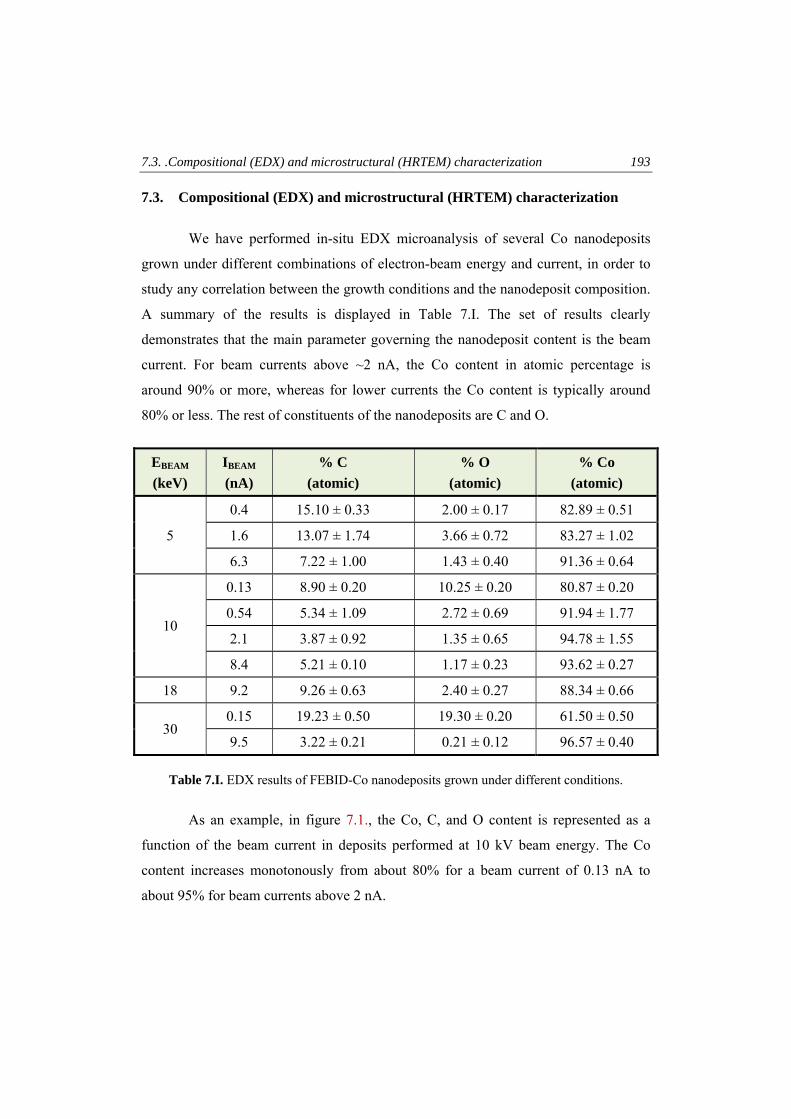
7.3. .Compositional (EDX) and microstructural (HRTEM) characterization 193
7.3. Compositional (EDX) and microstructural (HRTEM) characterization
We have performed in-situ EDX microanalysis of several Co nanodeposits
grown under different combinations of electron-beam energy and current, in order to
study any correlation between the growth conditions and the nanodeposit composition.
A summary of the results is displayed in Table 7.I. The set of results clearly
demonstrates that the main parameter governing the nanodeposit content is the beam
current. For beam currents above ~2 nA, the Co content in atomic percentage is
around 90% or more, whereas for lower currents the Co content is typically around
80% or less. The rest of constituents of the nanodeposits are C and O.
EBEAM (keV)
IBEAM (nA)
% C (atomic)
% O
(atomic) % Co
(atomic)
5
0.4 15.10 ± 0.33 2.00 ± 0.17 82.89 ± 0.51
1.6 13.07 ± 1.74 3.66 ± 0.72 83.27 ± 1.02
6.3 7.22 ± 1.00 1.43 ± 0.40 91.36 ± 0.64
10
0.13 8.90 ± 0.20 10.25 ± 0.20 80.87 ± 0.20
0.54 5.34 ± 1.09 2.72 ± 0.69 91.94 ± 1.77
2.1 3.87 ± 0.92 1.35 ± 0.65 94.78 ± 1.55
8.4 5.21 ± 0.10 1.17 ± 0.23 93.62 ± 0.27
18 9.2 9.26 ± 0.63 2.40 ± 0.27 88.34 ± 0.66
30 0.15 19.23 ± 0.50 19.30 ± 0.20 61.50 ± 0.50
9.5 3.22 ± 0.21 0.21 ± 0.12 96.57 ± 0.40
Table 7.I. EDX results of FEBID-Co nanodeposits grown under different conditions.
As an example, in figure 7.1., the Co, C, and O content is represented as a
function of the beam current in deposits performed at 10 kV beam energy. The Co
content increases monotonously from about 80% for a beam current of 0.13 nA to
about 95% for beam currents above 2 nA.
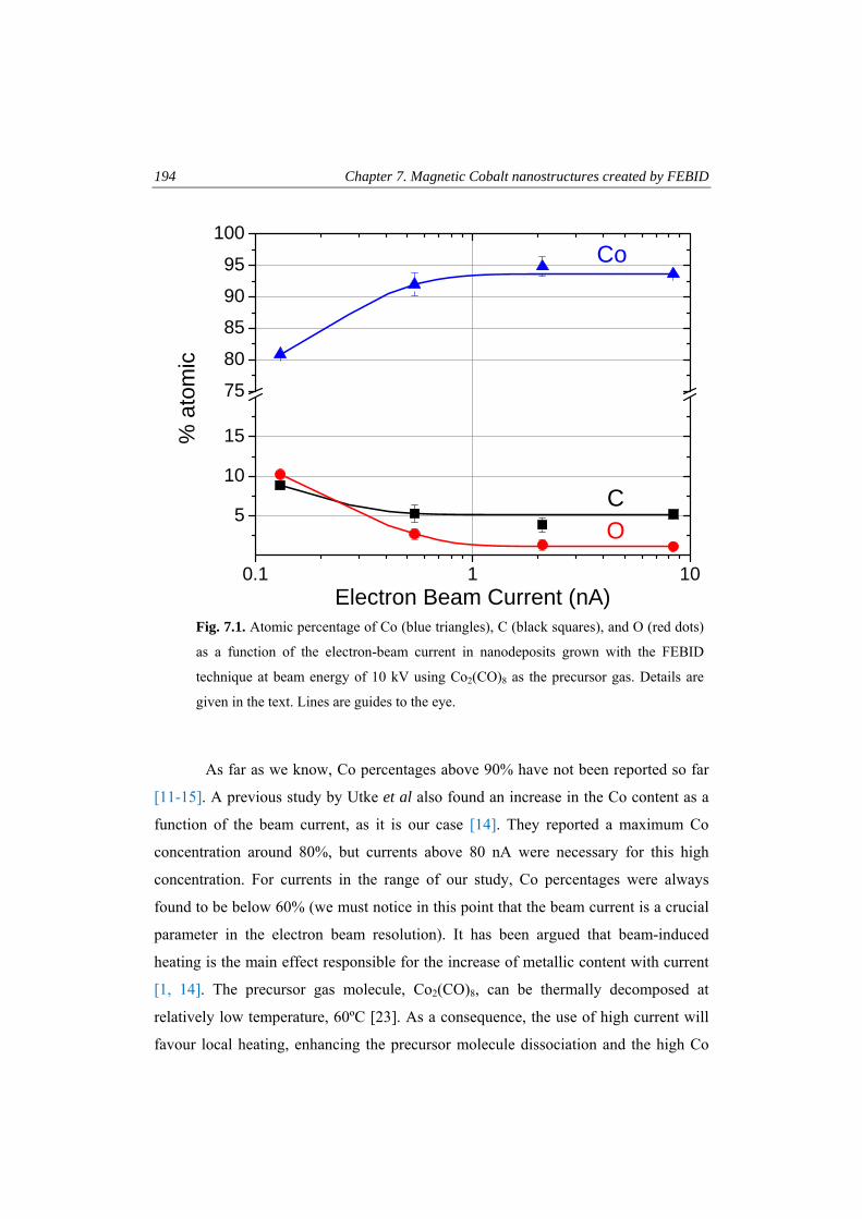
194 Chapter 7. Magnetic Cobalt nanostructures created by FEBID
As far as we know, Co percentages above 90% have not been reported so far
[11-15]. A previous study by Utke et al also found an increase in the Co content as a
function of the beam current, as it is our case [14]. They reported a maximum Co
concentration around 80%, but currents above 80 nA were necessary for this high
concentration. For currents in the range of our study, Co percentages were always
found to be below 60% (we must notice in this point that the beam current is a crucial
parameter in the electron beam resolution). It has been argued that beam-induced
heating is the main effect responsible for the increase of metallic content with current
[1, 14]. The precursor gas molecule, Co2(CO)8, can be thermally decomposed at
relatively low temperature, 60ºC [23]. As a consequence, the use of high current will
favour local heating, enhancing the precursor molecule dissociation and the high Co
0.1 1 10
5
10
15
75
80
85
90
95
100
OC
% a
tom
ic
Electron Beam Current (nA)
Co
Fig. 7.1. Atomic percentage of Co (blue triangles), C (black squares), and O (red dots)
as a function of the electron-beam current in nanodeposits grown with the FEBID
technique at beam energy of 10 kV using Co2(CO)8 as the precursor gas. Details are
given in the text. Lines are guides to the eye.
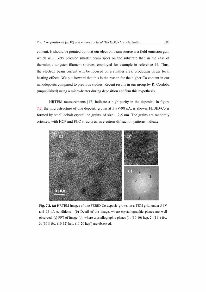
7.3. .Compositional (EDX) and microstructural (HRTEM) characterization 195
content. It should be pointed out that our electron beam source is a field-emission gun,
which will likely produce smaller beam spots on the substrate than in the case of
thermionic-tungsten-filament sources, employed for example in reference 14. Thus,
the electron beam current will be focused on a smaller area, producing larger local
heating effects. We put forward that this is the reason for the higher Co content in our
nanodeposits compared to previous studies. Recent results in our group by R. Córdoba
(unpublished) using a micro-heater during deposition confirm this hypothesis.
HRTEM measurements [17] indicate a high purity in the deposits. In figure
7.2. the microstructure of one deposit, grown at 5 kV/98 pA, is shown. FEBID-Co is
formed by small cobalt crystalline grains, of size ~ 2-5 nm. The grains are randomly
oriented, with HCP and FCC structures, as electron-diffraction patterns indicate.
Fig. 7.2. (a) HRTEM images of one FEBID-Co deposit grown on a TEM grid, under 5 kV
and 98 pA conditions. (b) Detail of the image, where crystallographic planes are well
observed. (c) FFT of image (b), where crystallographic planes [1: (10-10) hcp, 2: (111) fcc,
3: (101) fcc, (10-12) hcp, (11-20 hcp)] are observed.
a) b)
c)
5 µm
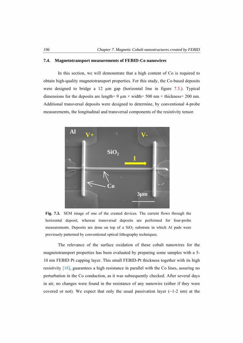
196 Chapter 7. Magnetic Cobalt nanostructures created by FEBID
7.4. Magnetotransport measurements of FEBID-Co nanowires
In this section, we will demonstrate that a high content of Co is required to
obtain high-quality magnetotransport properties. For this study, the Co-based deposits
were designed to bridge a 12 µm gap (horizontal line in figure 7.3.). Typical
dimensions for the deposits are length= 9 µm × width= 500 nm × thickness= 200 nm.
Additional transversal deposits were designed to determine, by conventional 4-probe
measurements, the longitudinal and transversal components of the resistivity tensor.
The relevance of the surface oxidation of these cobalt nanowires for the
magnetotransport properties has been evaluated by preparing some samples with a 5-
10 nm FEBID Pt capping layer. This small FEBID-Pt thickness together with its high
resistivity [18], guarantees a high resistance in parallel with the Co lines, assuring no
perturbation in the Co conduction, as it was subsequently checked. After several days
in air, no changes were found in the resistance of any nanowire (either if they were
covered or not). We expect that only the usual passivation layer (~1-2 nm) at the
3µm
Al
SiO2
Co 3µm3µm
Al
SiO2
Co
I
V+ V-
Fig. 7.3. SEM image of one of the created devices. The current flows through the
horizontal deposit, whereas transversal deposits are performed for four-probe
measurements. Deposits are done on top of a SiO2 substrate in which Al pads were
previously patterned by conventional optical lithography techniques.
7.4. Magnetotransport measurements of FEBID-Co nanowires 197
topmost surface will be present in the non-covered nanowires, without any significant
influence on the obtained results. This is not the general case in other deposits created
by focused beams [18].
7.4.1. Magnetotransport properties of cobalt NWs grown at high currents
As an example, we will show hereafter the results obtained on a NW grown
with a beam energy of 10 kV and a beam current of 2.1 nA, thus having a high Co
content (around 95%). A wide range of magnetic field-dependent transport
measurements has been performed.
In figure 7.4. we can see a typical resistivity-versus-temperature measurement
for this nanowire. The behaviour is not, as it is the general rule in FEBID deposits,
semiconducting-like [18], but fully metallic, confirming that the residual amount of
carbon in the sample is minimal. The resistivity at room temperature is of the order of
40 µΩcm, only a factor of 7 larger than in bulk polycrystalline cobalt. As will be
discussed later, this value of resistivity is just related to the small grain size of the
FEBID deposit. Another nanowire grown at 10 kV and 0.54 beam current, with Co
content around 92%, also displays similar resistivity value. These FEBID-Co deposits
are the most conductive ones found in literature. The Residual Resistivity Ratio
(RRR=ρ300K/ρ2K) is about 1.3, in agreement with results for polycrystalline cobalt thin
films [19].
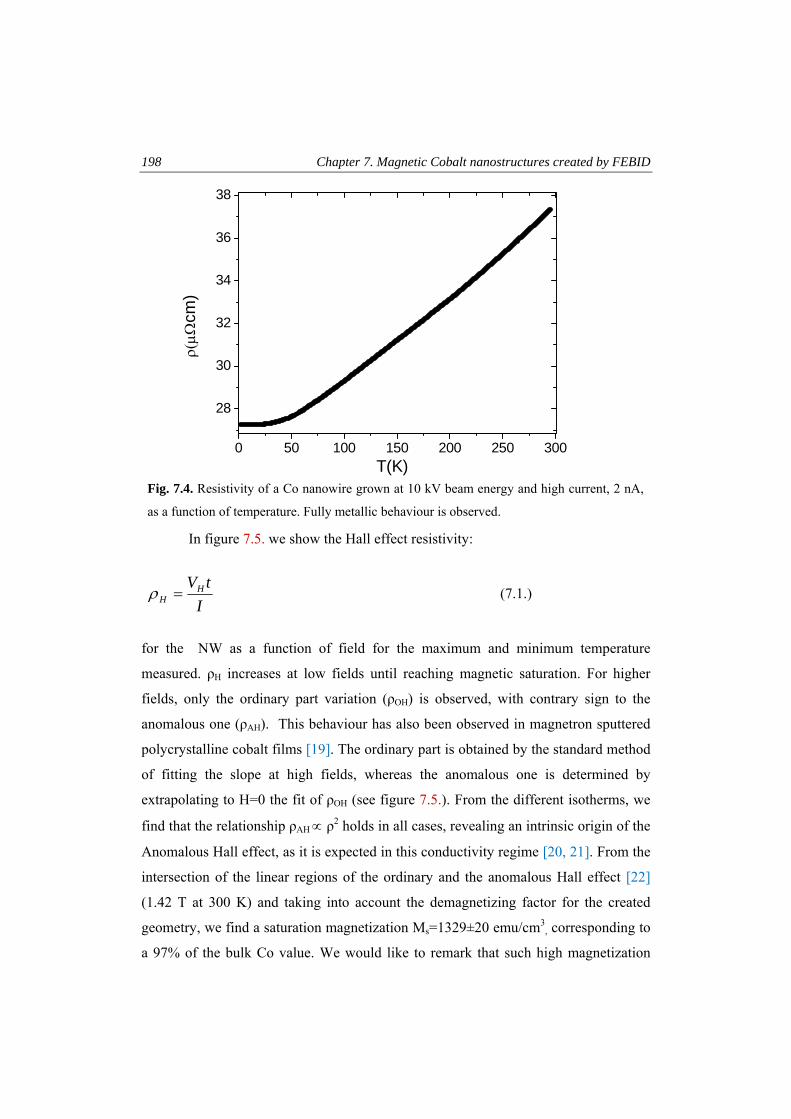
198 Chapter 7. Magnetic Cobalt nanostructures created by FEBID
In figure 7.5. we show the Hall effect resistivity:
ItVH
H =ρ (7.1.)
for the NW as a function of field for the maximum and minimum temperature
measured. ρH increases at low fields until reaching magnetic saturation. For higher
fields, only the ordinary part variation (ρOH) is observed, with contrary sign to the
anomalous one (ρAH). This behaviour has also been observed in magnetron sputtered
polycrystalline cobalt films [19]. The ordinary part is obtained by the standard method
of fitting the slope at high fields, whereas the anomalous one is determined by
extrapolating to H=0 the fit of ρOH (see figure 7.5.). From the different isotherms, we
find that the relationship ρAH ∝ ρ2 holds in all cases, revealing an intrinsic origin of the
Anomalous Hall effect, as it is expected in this conductivity regime [20, 21]. From the
intersection of the linear regions of the ordinary and the anomalous Hall effect [22]
(1.42 T at 300 K) and taking into account the demagnetizing factor for the created
geometry, we find a saturation magnetization Ms=1329±20 emu/cm3, corresponding to
a 97% of the bulk Co value. We would like to remark that such high magnetization
Fig. 7.4. Resistivity of a Co nanowire grown at 10 kV beam energy and high current, 2 nA,
as a function of temperature. Fully metallic behaviour is observed.
0 50 100 150 200 250 300
28
30
32
34
36
38
ρ(μΩ
cm)
T(K)
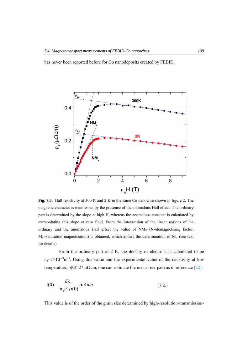
7.4. Magnetotransport measurements of FEBID-Co nanowires 199
has never been reported before for Co nanodeposits created by FEBID.
From the ordinary part at 2 K, the density of electrons is calculated to be
ne=7×10-28m-3. Using this value and the experimental value of the resistivity at low
temperature, ρ(0)≈27 µΩcm, one can estimate the mean-free-path as in reference [22]:
nme
4)0(n
k=l(0) 2
e
F ≈ρ
h (7.2.)
This value is of the order of the grain size determined by high-resolution-transmission-
0 2 4 6 80.0
0.2
0.4
NMs
ρAH
NMs
2K
ρ H(μΩ
cm)
μoH (T)
300KρAH
Fig. 7.5. Hall resistivity at 300 K and 2 K in the same Co nanowire shown in figure 2. The
magnetic character is manifested by the presence of the anomalous Hall effect. The ordinary
part is determined by the slope at high H, whereas the anomalous constant is calculated by
extrapolating this slope at zero field. From the intersection of the linear regions of the
ordinary and the anomalous Hall effect the value of NMS (N=demagnetising factor,
MS=saturation magnetization) is obtained, which allows the determination of Ms (see text
for details).
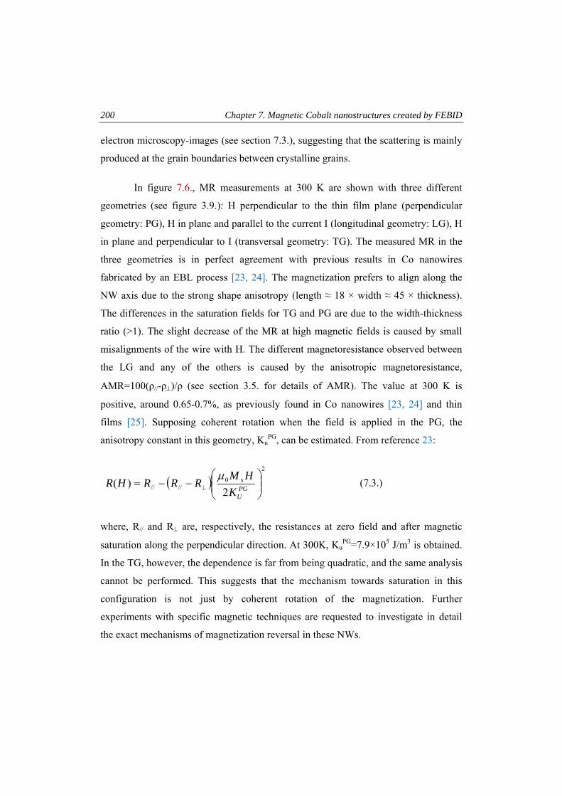
200 Chapter 7. Magnetic Cobalt nanostructures created by FEBID
electron microscopy-images (see section 7.3.), suggesting that the scattering is mainly
produced at the grain boundaries between crystalline grains.
In figure 7.6., MR measurements at 300 K are shown with three different
geometries (see figure 3.9.): H perpendicular to the thin film plane (perpendicular
geometry: PG), H in plane and parallel to the current I (longitudinal geometry: LG), H
in plane and perpendicular to I (transversal geometry: TG). The measured MR in the
three geometries is in perfect agreement with previous results in Co nanowires
fabricated by an EBL process [23, 24]. The magnetization prefers to align along the
NW axis due to the strong shape anisotropy (length ≈ 18 × width ≈ 45 × thickness).
The differences in the saturation fields for TG and PG are due to the width-thickness
ratio (>1). The slight decrease of the MR at high magnetic fields is caused by small
misalignments of the wire with H. The different magnetoresistance observed between
the LG and any of the others is caused by the anisotropic magnetoresistance,
AMR=100(ρ//-ρ⊥)/ρ (see section 3.5. for details of AMR). The value at 300 K is
positive, around 0.65-0.7%, as previously found in Co nanowires [23, 24] and thin
films [25]. Supposing coherent rotation when the field is applied in the PG, the
anisotropy constant in this geometry, KuPG, can be estimated. From reference 23:
( )2
0//// 2
)( ⎟⎟⎠
⎞⎜⎜⎝
⎛−−= ⊥ PG
U
s
KHM
RRRHRμ
(7.3.)
where, R// and R⊥ are, respectively, the resistances at zero field and after magnetic
saturation along the perpendicular direction. At 300K, KuPG=7.9×10⁵ J/m3 is obtained.
In the TG, however, the dependence is far from being quadratic, and the same analysis
cannot be performed. This suggests that the mechanism towards saturation in this
configuration is not just by coherent rotation of the magnetization. Further
experiments with specific magnetic techniques are requested to investigate in detail
the exact mechanisms of magnetization reversal in these NWs.
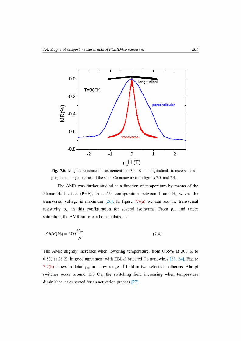
7.4. Magnetotransport measurements of FEBID-Co nanowires 201
The AMR was further studied as a function of temperature by means of the
Planar Hall effect (PHE), in a 45º configuration between I and H, where the
transversal voltage is maximum [26]. In figure 7.7(a) we can see the transversal
resistivity ρxy in this configuration for several isotherms. From ρxy and under
saturation, the AMR ratios can be calculated as
ρρ xyAMR 200(%) = (7.4.)
The AMR slightly increases when lowering temperature, from 0.65% at 300 K to
0.8% at 25 K, in good agreement with EBL-fabricated Co nanowires [23, 24]. Figure
7.7(b) shows in detail ρxy in a low range of field in two selected isotherms. Abrupt
switches occur around 150 Oe, the switching field increasing when temperature
diminishes, as expected for an activation process [27].
Fig. 7.6. Magnetoresistance measurements at 300 K in longitudinal, transversal and
perpendicular geometries of the same Co nanowire as in figures 7.5. and 7.4.
-2 -1 0 1 2-0.8
-0.6
-0.4
-0.2
0.0
perpendicular
transversal
MR
(%)
μoH (T)
longitudinal
T=300K
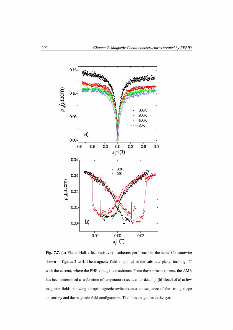
202 Chapter 7. Magnetic Cobalt nanostructures created by FEBID
-0.9 -0.6 -0.3 0.0 0.3 0.6 0.90.00
0.05
0.10
0.15
ρ H(μΩ
cm)
300K 200K 100K 25K
μoH (T)
a)
-0.02 0.00 0.02
0.00
0.01
0.02
0.03
0.04
300K 25K
ρ H(μΩ
cm)
μoH(T)
b)
Fig. 7.7. (a) Planar Hall effect resistivity isotherms performed in the same Co nanowire
shown in figures 2 to 4. The magnetic field is applied in the substrate plane, forming 45º
with the current, where the PHE voltage is maximum. From these measurements, the AMR
has been determined as a function of temperature (see text for details). (b) Detail of a) at low
magnetic fields, showing abrupt magnetic switches as a consequence of the strong shape
anisotropy and the magnetic field configuration. The lines are guides to the eye.
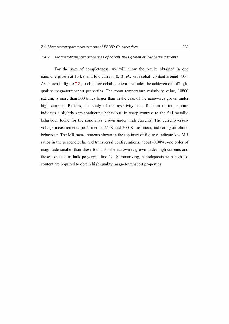
7.4. Magnetotransport measurements of FEBID-Co nanowires 203
7.4.2. Magnetotransport properties of cobalt NWs grown at low beam currents
For the sake of completeness, we will show the results obtained in one
nanowire grown at 10 kV and low current, 0.13 nA, with cobalt content around 80%.
As shown in figure 7.8., such a low cobalt content precludes the achievement of high-
quality magnetotransport properties. The room temperature resistivity value, 10800
µΩ cm, is more than 300 times larger than in the case of the nanowires grown under
high currents. Besides, the study of the resistivity as a function of temperature
indicates a slightly semiconducting behaviour, in sharp contrast to the full metallic
behaviour found for the nanowires grown under high currents. The current-versus-
voltage measurements performed at 25 K and 300 K are linear, indicating an ohmic
behaviour. The MR measurements shown in the top inset of figure 6 indicate low MR
ratios in the perpendicular and transversal configurations, about -0.08%, one order of
magnitude smaller than those found for the nanowires grown under high currents and
those expected in bulk polycrystalline Co. Summarizing, nanodeposits with high Co
content are required to obtain high-quality magnetotransport properties.
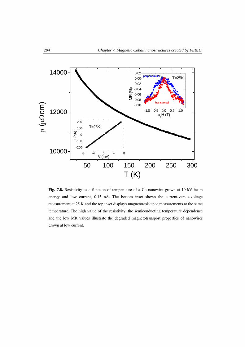
204 Chapter 7. Magnetic Cobalt nanostructures created by FEBID
50 100 150 200 250 300
10000
12000
14000
-1.0 -0.5 0.0 0.5 1.0-0.10-0.08-0.06-0.04-0.020.000.02
μoH (T)
transversal
MR
(%)
perpendicular T=25K
ρ (μΩ
cm)
T (K)
-8 -4 0 4 8
-200
-100
0
100
200
I (nA
)
V (mV)
T=25K
Fig. 7.8. Resistivity as a function of temperature of a Co nanowire grown at 10 kV beam
energy and low current, 0.13 nA. The bottom inset shows the current-versus-voltage
measurement at 25 K and the top inset displays magnetoresistance measurements at the same
temperature. The high value of the resistivity, the semiconducting temperature dependence
and the low MR values illustrate the degraded magnetotransport properties of nanowires
grown at low current.
7.5. Systematic MOKE study of rectangular nanowires 205
7.5. Systematic MOKE study of rectangular nanowires
After having demonstrated that FEBID-Co is really pure, in this section, we
will show a systematic study, by means of spatially-resolved magneto-optical Kerr
effect (MOKE), of the magnetic hysteresis loops of single wires in a wide range of
aspect ratios, and grown under different beam currents. The dependence of the
switching fields with the dimensions is studied, and compared with analogous
structures fabricated by other techniques. This study tries to understand the
mechanisms for the reversal of the magnetization for these structures. This has been
under intense study for the last decade [23, 28-33], due to its relevance in Spintronics
applications [34].
7.5.1. Types of structures grown. Maximum resolution obtained.
The rectangular deposits were grown at 5 kV, with beam currents (IFEB) = 0.4,
1.6, 6.3 and 24 nA. Two types of substrates were used for these experiments: a silicon
wafer (type I), and a 200 nm-thick SiO2 layer on top of Si, created by a thermal
oxidation process (type II). The dimensions of the rectangular lines were: length (L) =
8 or 4 µm (no difference was found for same aspect ratio), thickness (t) = 200 or 50
nm. The nominal widths (w) were chosen to have structures with aspect ratios
(AR=L/w) varying from 1 up to 32 (16). The study was complemented by depositing
single-pixel-line wires using the smallest beam current selected, IBEAM= 0.4 nA. The
aim to grow these lines was to determine the best resolution in width attained under
conditions appropriate for reasonably high Co content (see table 7.I.). The wire width
will presumably be bigger than the FEB spot size, as a consequence of the interaction
volume of the electrons with the substrate [1, 2]. The minimum width was found to
have a full width at half maximum of around 150 nm for a 40 nm-thick deposit
(corresponding to an AR =26 for L=4 µm).
In figure 7.9., some examples of SEM images of lines deposited in both
substrates are shown. Additionally to the main line, a parasitic deposit around the
structure is present (ranging, in one y-direction, between 400 nm up to 1 µm, as
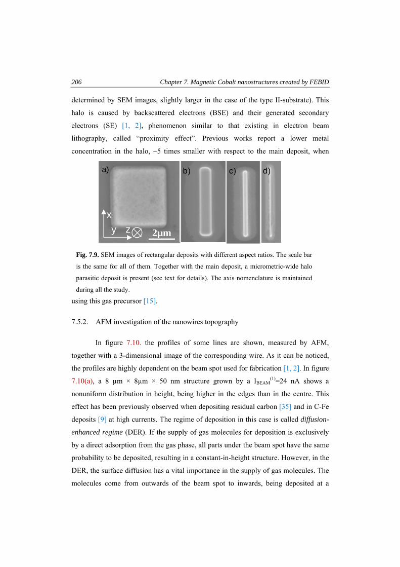
206 Chapter 7. Magnetic Cobalt nanostructures created by FEBID
determined by SEM images, slightly larger in the case of the type II-substrate). This
halo is caused by backscattered electrons (BSE) and their generated secondary
electrons (SE) [1, 2], phenomenon similar to that existing in electron beam
lithography, called “proximity effect”. Previous works report a lower metal
concentration in the halo, ~5 times smaller with respect to the main deposit, when
using this gas precursor [15].
7.5.2. AFM investigation of the nanowires topography
In figure 7.10. the profiles of some lines are shown, measured by AFM,
together with a 3-dimensional image of the corresponding wire. As it can be noticed,
the profiles are highly dependent on the beam spot used for fabrication [1, 2]. In figure
7.10(a), a 8 µm × 8µm × 50 nm structure grown by a IBEAM(1)=24 nA shows a
nonuniform distribution in height, being higher in the edges than in the centre. This
effect has been previously observed when depositing residual carbon [35] and in C-Fe
deposits [9] at high currents. The regime of deposition in this case is called diffusion-
enhanced regime (DER). If the supply of gas molecules for deposition is exclusively
by a direct adsorption from the gas phase, all parts under the beam spot have the same
probability to be deposited, resulting in a constant-in-height structure. However, in the
DER, the surface diffusion has a vital importance in the supply of gas molecules. The
molecules come from outwards of the beam spot to inwards, being deposited at a
2µmyx
z
a) b) c) d)
Fig. 7.9. SEM images of rectangular deposits with different aspect ratios. The scale bar
is the same for all of them. Together with the main deposit, a micrometric-wide halo
parasitic deposit is present (see text for details). The axis nomenclature is maintained
during all the study.
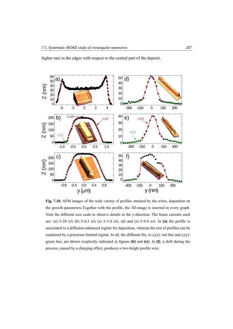
7.5. Systematic MOKE study of rectangular nanowires 207
higher rate in the edges with respect to the central part of the deposit.
Fig. 7.10. AFM images of the wide variety of profiles attained by the wires, dependent on
the growth parameters.Together with the profile, the 3D-image is inserted in every graph.
Note the different axis scale to observe details in the y-direction. The beam currents used
are: (a) I=24 nA (b) I=6.3 nA (c) I=1.6 nA, (d) and (e) I=0.4 nA. In (a) the profile is
associated to a diffusion-enhanced regime for deposition, whereas the rest of profiles can be
explained by a precursor-limited regime. In all, the different fits, to z2(y): red line and z3(y):
green line, are shown (explicitly indicated in figures (b) and (e)). In (f), a shift during the
process, caused by a charging effect, produces a two-height profile wire.
a)
b)
c)
d)
e)
f)
-4 -2 0 2 40
102030405060
-300 -150 0 150 300
01020304050
-1.0 -0.5 0.0 0.5 1.00
50
100
150
200
-300 -150 0 150 3000
1020304050
-0.8 -0.4 0.0 0.4 0.80
50100150200
-300 -150 0 150 3000
10
20
30
40
Z (n
m)
Z (n
m)
y (nm)
Z (n
m)
y (μm)
z3(y)
z2(y)
z3(y)
z2(y)z1 (y)
208 Chapter 7. Magnetic Cobalt nanostructures created by FEBID
For the rest of beam currents used this effect is not important, resulting in an
approximately constant height in the central part of the structure. In this case, the
regime for deposition is called precursor-limited regime (PLR), since the use of
relatively high currents with a moderate gas pressure results in a deposition induced
by a direct supply from the gas phase. In figure 7.10(b) and 7.10(c) lines deposited
with IBEAM(2)=6.3 nA and IBEAM
(3)=1.6 nA, respectively, are shown. Figures 7.10(d), (e)
and (f) are profiles for structures with IBEAM(4)=0.4 nA. The wire in 7.10(e) was grown
by a single-pixel-line process (in the rest, the beam defines a rectangular profile when
scanning). The structural profiles along the y direction,were fitted to a general
function:
101 )( yyforzyz <= (7.5(a))
Δ+<<⎟⎟⎠
⎞⎜⎜⎝
⎛ −= 112
2
2 2exp)( yyyfor
yAyz
σ (7.5(b))
Δ+>⎟⎟⎠
⎞⎜⎜⎝
⎛ −= 1*3 exp)( yyfor
y
yByz (7.5(c))
In the following, a deeper description of these profiles is given. Equation
(7.5(a)) gives account of the constant height in the centre of the structure when
fabricating wide structures, as a consequence of the good beam overlap (see for
instance figures 7.10(b) and (c)). The bigger height in the edges in the DER is
therefore not considered in this model. The mean roughness for this central part was
found to be typically around 10 nm. Gaussian fits of the tails of the deposit (equation
(7.5(b)) are shown in figure 7.10, as red lines. The full width at half maximum
(FWHM) of them depends on the beam current, being approximately of 500 nm for
IBEAM(1), IBEAM
(2) and IBEAM(3), and of 150 nm for IBEAM
(4). This dimension is several
times higher than the gaussian primary beams used, and is caused by the generation of
SE in the substrate in a larger volume than that targeted by the primary beam. Monte-
Carlo simulations evidence this effect [1, 2]. The most external, exponential part of the
7.5. Systematic MOKE study of rectangular nanowires 209
profile (equation 7.5(c)) corresponds to the halo deposit explained in the previous
section, occurring as a consequence of the generation of BSE when irradiating the
substrate. This picture can be understood using the Bethe stopping-power formula [12,
36]. The parameter y* was found to be of the order of a few hundreds of nanometers.
Lower currents than those used here would have resulted in a crossover to the
electron-limited regime (ELR), where the replenishment rate of molecules would be
higher than the dissociation rate of gas molecules. The profiles in this regime are
sharper [1, 2], but we intentionally did not use small currents since the purity of the
FEBID-Co is substantially smaller for low beam currents, as was deeply studied in
sections 7.4.1 and 7.4.2.
It is interesting to include figure 7.10(f), where a deposit with a two-step
height was imaged. This structure was grown on SiO2, and as a consequence of the
charging effect by the progressive accumulation of the irradiated charge, a beam shift
occurred during its growth. The grounding of the substrate near the place of interest,
by the contact of a commercial Omniprobe needle, was used to avoid this effect in
most of the deposits. As we will show in next section, this has relevant influence in the
magnetic properties, Magnetization hysteresis loops by MOKE measurements
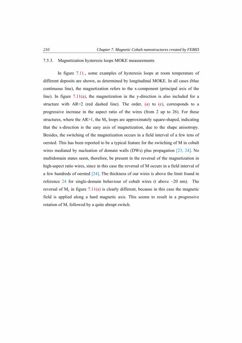
210 Chapter 7. Magnetic Cobalt nanostructures created by FEBID
7.5.3. Magnetization hysteresis loops MOKE measurements
In figure 7.11., some examples of hysteresis loops at room temperature of
different deposits are shown, as determined by longitudinal MOKE. In all cases (blue
continuous line), the magnetization refers to the x-component (principal axis of the
line). In figure 7.11(a), the magnetization in the y-direction is also included for a
structure with AR=2 (red dashed line). The order, (a) to (e), corresponds to a
progressive increase in the aspect ratio of the wires (from 2 up to 26). For these
structures, where the AR>1, the Mx loops are approximately square-shaped, indicating
that the x-direction is the easy axis of magnetization, due to the shape anisotropy.
Besides, the switching of the magnetization occurs in a field interval of a few tens of
oersted. This has been reported to be a typical feature for the switching of M in cobalt
wires mediated by nucleation of domain walls (DWs) plus propagation [23, 24]. No
multidomain states seem, therefore, be present in the reversal of the magnetization in
high-aspect ratio wires, since in this case the reversal of M occurs in a field interval of
a few hundreds of oersted [24]. The thickness of our wires is above the limit found in
reference 24 for single-domain behaviour of cobalt wires (t above ~20 nm). The
reversal of My in figure 7.11(a) is clearly different, because in this case the magnetic
field is applied along a hard magnetic axis. This seems to result in a progressive
rotation of M, followed by a quite abrupt switch.
7.5. Systematic MOKE study of rectangular nanowires 211
The MOKE loop in figure 7.11(f) corresponds to a structure analogous to that
shown in figure 7.10(f), with a two-step height profile, caused by a shift during the
growth. This profile results in a two-step switch of M.
Experiments devoted to determine the importance of the halo in the
magnetism of the wires were done, by focusing the laser spot exclusively on that zone,
out of the main structure, and performing hysteresis loops. We did not obtain a
relevant magnetic signal in any case, indicating the low magnetic character of this
second-order deposit. Thus, we conclude that although SEM images show a total
structure extending for a few microns in the x-y plane, the structure grown is
ferromagnetic only in the main wire. The reduced thickness (AFM images, figure
7.10.), more susceptible to a complete oxidation, together with a significant higher
carbon+oxygen/cobalt ratio present in the halo with respect to the main deposit, as
preliminary measurements with a STEM microscope indicate [37], are in perfect
consonance with these conclusions obtained from MOKE measurements. This result is
not general for FEBID processes, since for instance, the contrary effect has been
reported in iron deposits grown by FEBID using Fe(CO)5 as gas precursor [7].
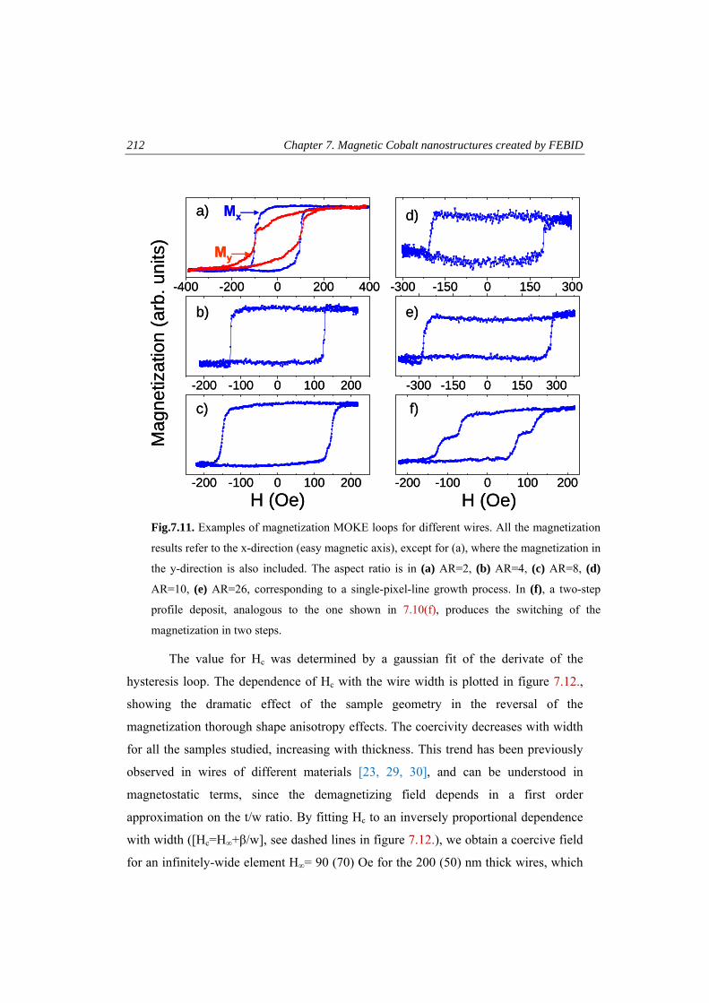
212 Chapter 7. Magnetic Cobalt nanostructures created by FEBID
The value for Hc was determined by a gaussian fit of the derivate of the
hysteresis loop. The dependence of Hc with the wire width is plotted in figure 7.12.,
showing the dramatic effect of the sample geometry in the reversal of the
magnetization thorough shape anisotropy effects. The coercivity decreases with width
for all the samples studied, increasing with thickness. This trend has been previously
observed in wires of different materials [23, 29, 30], and can be understood in
magnetostatic terms, since the demagnetizing field depends in a first order
approximation on the t/w ratio. By fitting Hc to an inversely proportional dependence
with width ([Hc=H∞+β/w], see dashed lines in figure 7.12.), we obtain a coercive field
for an infinitely-wide element H∞= 90 (70) Oe for the 200 (50) nm thick wires, which
a)
b)
c)
d)
e)
f)
Mx
My
-400 -200 0 200 400 -300 -150 0 150 300
-200 -100 0 100 200 -300 -150 0 150 300
-200 -100 0 100 200 -200 -100 0 100 200
Mag
netiz
atio
n (a
rb. u
nits
)
H (Oe)H (Oe)
a)
b)
c)
d)
e)
f)
Mx
My
-400 -200 0 200 400 -300 -150 0 150 300
-200 -100 0 100 200 -300 -150 0 150 300
-200 -100 0 100 200 -200 -100 0 100 200
Mag
netiz
atio
n (a
rb. u
nits
)
H (Oe)H (Oe)
Fig.7.11. Examples of magnetization MOKE loops for different wires. All the magnetization
results refer to the x-direction (easy magnetic axis), except for (a), where the magnetization in
the y-direction is also included. The aspect ratio is in (a) AR=2, (b) AR=4, (c) AR=8, (d)
AR=10, (e) AR=26, corresponding to a single-pixel-line growth process. In (f), a two-step
profile deposit, analogous to the one shown in 7.10(f), produces the switching of the
magnetization in two steps.
7.5. Systematic MOKE study of rectangular nanowires 213
is a reasonable value for a cobalt polycrystalline thin film. If, on the contrary, the field
derived from this fit is made equal to the coherent rotation switching field value,
Hc=2πMs ~ 8350 Oe (Ms value determined by magnetotrasport measurements, see
section 7.4.1), we obtain an equivalent width of 3.5 and 7 nm, for thickness of 50 and
200 nm, respectively. These widths are compatible with the expected lateral wire
dimension, of the order of the exchange length value, ~ 5 nm in Co [30]. These results
are in perfect agreement with ref. 23 and 30, where Co wires fabricated by EBL were
analysed in the same manner.
On the other hand, Uhlig et al [30] described the dependence of Hc with shape
in cobalt and permalloy nanolines as:
wtbMaH s
c += (7.6.)
finding a universal dependence, since b=3 in all cases. This factor is related with the
in-plane aspect ratio (L/w) of the volume in the wire responsible for the magnetization
reversal, assuming coherent rotation in this critical nucleus, and applying a Stoner-
Wolfharth analysis [38]. b=3 means that the in-plane area for the reversal is 1.25w2.
From our results, we find that the area that induces the reversal of M in our wires is
(1.20 ± 0.05)w2 for the 50 nm-thick deposits, and (1.50 ± 0.06)w2 for the 200 nm-
thick structures. Thus, both dependences do not collapse exactly to the same value.
Nevertheless, the lack of accuracy in the determination of the exact dimensions of the
wires, the different profiles they have, as well as possible changes in the purity and
microstructure of the deposits with the beam current can induce these small
differences. The remarkable conclusion from this analysis is that the volume involved
in the initial reversal of M is very different from the whole structure. The reversal
process is dominated by the formation of domain walls at the surfaces of the wire
width, near the edges (as it will be shown in section 3.3) or surrounding existing
defects, which will be propagated trough the whole wire when a magnetic field is
applied. The minimization of the magnetostatic energy, by avoiding surface magnetic
charges, causes this behaviour. Thus, the ‘‘effective’’ volume appears to be a localized
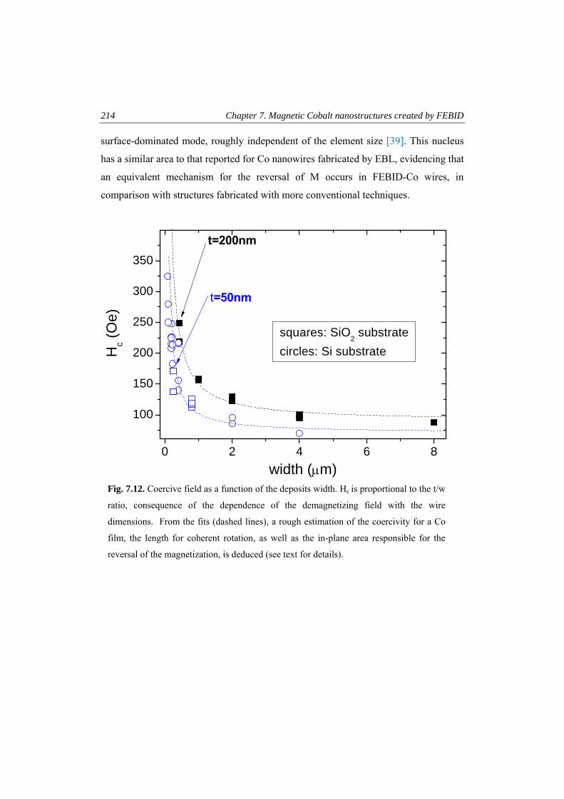
214 Chapter 7. Magnetic Cobalt nanostructures created by FEBID
surface-dominated mode, roughly independent of the element size [39]. This nucleus
has a similar area to that reported for Co nanowires fabricated by EBL, evidencing that
an equivalent mechanism for the reversal of M occurs in FEBID-Co wires, in
comparison with structures fabricated with more conventional techniques.
0 2 4 6 8
100
150
200
250
300
350
t=50nm
Hc (O
e)
width (μm)
t=200nm
squares: SiO2 substratecircles: Si substrate
Fig. 7.12. Coercive field as a function of the deposits width. Hc is proportional to the t/w
ratio, consequence of the dependence of the demagnetizing field with the wire
dimensions. From the fits (dashed lines), a rough estimation of the coercivity for a Co
film, the length for coherent rotation, as well as the in-plane area responsible for the
reversal of the magnetization, is deduced (see text for details).
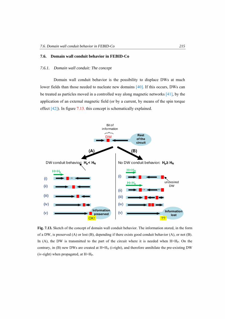
7.6. Domain wall conduit behavior in FEBID-Co 215
7.6. Domain wall conduit behavior in FEBID-Co
7.6.1. Domain wall conduit: The concept
Domain wall conduit behavior is the possibility to displace DWs at much
lower fields than those needed to nucleate new domains [40]. If this occurs, DWs can
be treated as particles moved in a controlled way along magnetic networks [41], by the
application of an external magnetic field (or by a current, by means of the spin torque
effect [42]). In figure 7.13. this concept is schematically explained.
Fig. 7.13. Sketch of the concept of domain wall conduit behavior. The information stored, in the form
of a DW, is preserved (A) or lost (B), depending if there exists good conduit behavior (A), or not (B).
In (A), the DW is transmitted to the part of the circuit where it is needed when H=HP. On the
contrary, in (B) new DWs are created at H=HN (i-right), and therefore annihilate the pre-existing DW
(iv-right) when propagated, at H=HP.
H=Hp
DW Restof thecircuit
DW conduit behavior: Hp< HN
Information preserved
OK!
(i)
(ii)
(iii)
(iv)
(v)
No DW conduit behavior: Hp≥ HN
H=HN
Information lost
??
H=Hp
(i)
(ii)
(iii)
(iv)
(v)
(A) (B)
Bit of information
undesiredDW
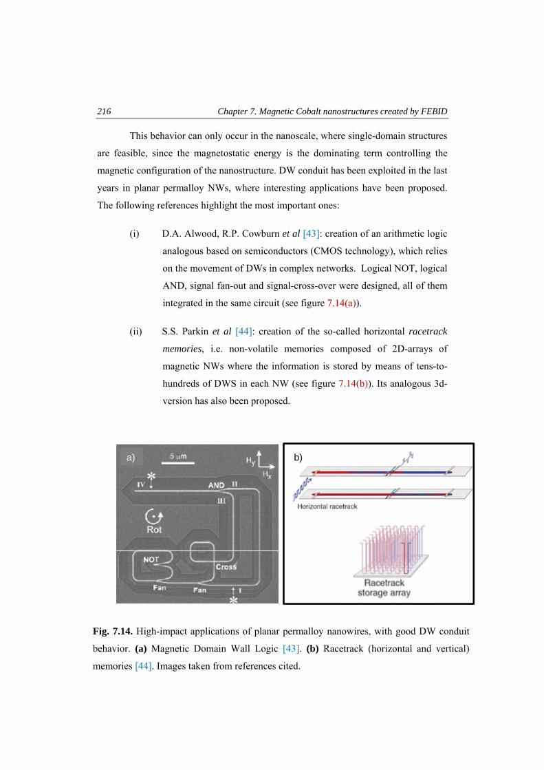
216 Chapter 7. Magnetic Cobalt nanostructures created by FEBID
This behavior can only occur in the nanoscale, where single-domain structures
are feasible, since the magnetostatic energy is the dominating term controlling the
magnetic configuration of the nanostructure. DW conduit has been exploited in the last
years in planar permalloy NWs, where interesting applications have been proposed.
The following references highlight the most important ones:
(i) D.A. Alwood, R.P. Cowburn et al [43]: creation of an arithmetic logic
analogous based on semiconductors (CMOS technology), which relies
on the movement of DWs in complex networks. Logical NOT, logical
AND, signal fan-out and signal-cross-over were designed, all of them
integrated in the same circuit (see figure 7.14(a)).
(ii) S.S. Parkin et al [44]: creation of the so-called horizontal racetrack
memories, i.e. non-volatile memories composed of 2D-arrays of
magnetic NWs where the information is stored by means of tens-to-
hundreds of DWS in each NW (see figure 7.14(b)). Its analogous 3d-
version has also been proposed.
a) b)
Fig. 7.14. High-impact applications of planar permalloy nanowires, with good DW conduit
behavior. (a) Magnetic Domain Wall Logic [43]. (b) Racetrack (horizontal and vertical)
memories [44]. Images taken from references cited.
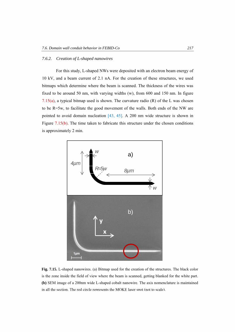
7.6. Domain wall conduit behavior in FEBID-Co 217
7.6.2. Creation of L-shaped nanowires
For this study, L-shaped NWs were deposited with an electron beam energy of
10 kV, and a beam current of 2.1 nA. For the creation of these structures, we used
bitmaps which determine where the beam is scanned. The thickness of the wires was
fixed to be around 50 nm, with varying widths (w), from 600 and 150 nm. In figure
7.15(a), a typical bitmap used is shown. The curvature radio (R) of the L was chosen
to be R=5w, to facilitate the good movement of the walls. Both ends of the NW are
pointed to avoid domain nucleation [43, 45]. A 200 nm wide structure is shown in
Figure 7.15(b). The time taken to fabricate this structure under the chosen conditions
is approximately 2 min.
Fig. 7.15. L-shaped nanowires. (a) Bitmap used for the creation of the structures. The black color
is the zone inside the field of view where the beam is scanned, getting blanked for the white part.
(b) SEM image of a 200nm wide L-shaped cobalt nanowire. The axis nomenclature is maintained
in all the section. The red circle represents the MOKE laser spot (not to scale).
8µm4µm
R=5w
w
w
y
x
a)
b)
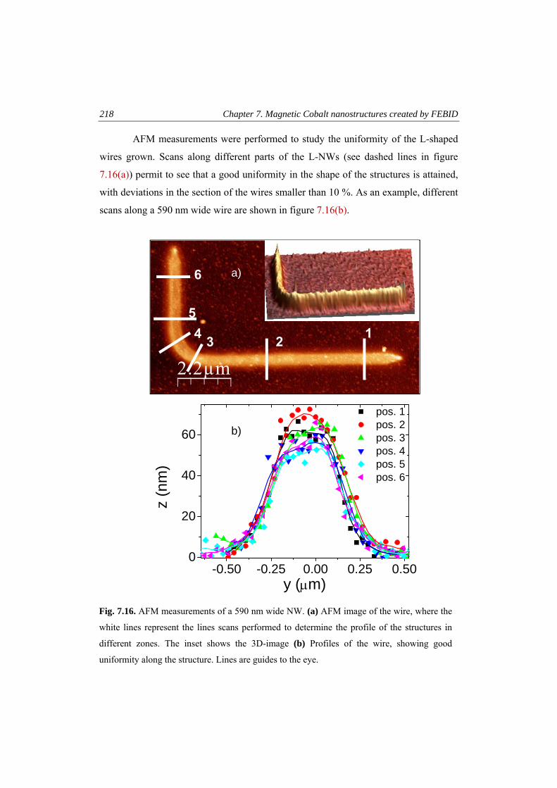
218 Chapter 7. Magnetic Cobalt nanostructures created by FEBID
AFM measurements were performed to study the uniformity of the L-shaped
wires grown. Scans along different parts of the L-NWs (see dashed lines in figure
7.16(a)) permit to see that a good uniformity in the shape of the structures is attained,
with deviations in the section of the wires smaller than 10 %. As an example, different
scans along a 590 nm wide wire are shown in figure 7.16(b).
Fig. 7.16. AFM measurements of a 590 nm wide NW. (a) AFM image of the wire, where the
white lines represent the lines scans performed to determine the profile of the structures in
different zones. The inset shows the 3D-image (b) Profiles of the wire, showing good
uniformity along the structure. Lines are guides to the eye.
2.2µm
12345
6
-0.50 -0.25 0.00 0.25 0.500
20
40
60
z (n
m)
y (μm)
pos. 1 pos. 2 pos. 3 pos. 4 pos. 5 pos. 6
b)
a)
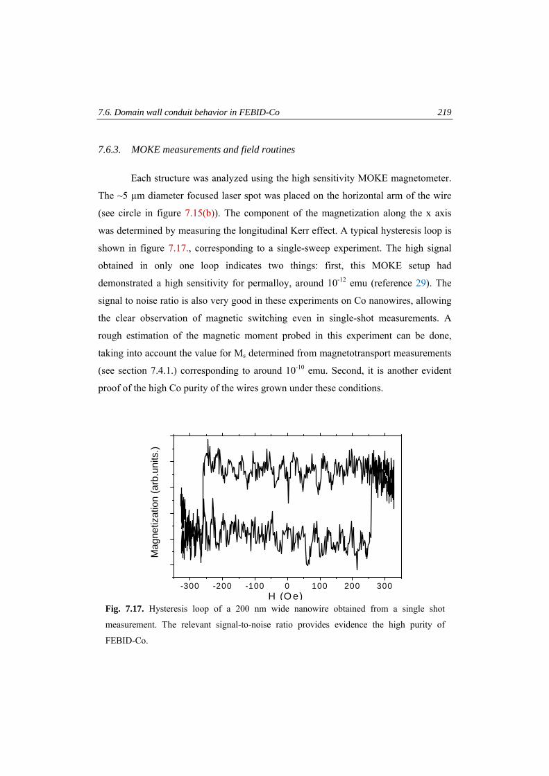
7.6. Domain wall conduit behavior in FEBID-Co 219
7.6.3. MOKE measurements and field routines
Each structure was analyzed using the high sensitivity MOKE magnetometer.
The ~5 µm diameter focused laser spot was placed on the horizontal arm of the wire
(see circle in figure 7.15(b)). The component of the magnetization along the x axis
was determined by measuring the longitudinal Kerr effect. A typical hysteresis loop is
shown in figure 7.17., corresponding to a single-sweep experiment. The high signal
obtained in only one loop indicates two things: first, this MOKE setup had
demonstrated a high sensitivity for permalloy, around 10-12 emu (reference 29). The
signal to noise ratio is also very good in these experiments on Co nanowires, allowing
the clear observation of magnetic switching even in single-shot measurements. A
rough estimation of the magnetic moment probed in this experiment can be done,
taking into account the value for Ms determined from magnetotransport measurements
(see section 7.4.1.) corresponding to around 10-10 emu. Second, it is another evident
proof of the high Co purity of the wires grown under these conditions.
-300 -200 -100 0 100 200 300
Mag
netiz
atio
n (a
rb.u
nits
.)
H (O e)Fig. 7.17. Hysteresis loop of a 200 nm wide nanowire obtained from a single shot
measurement. The relevant signal-to-noise ratio provides evidence the high purity of
FEBID-Co.
220 Chapter 7. Magnetic Cobalt nanostructures created by FEBID
To study the possible good control of DWs of the FEBID-Co, a quadrupole
electromagnet was used to apply two types of (Hx, Hy) magnetic field sequences at a
frequency of 1 Hz [46]. In the first procedure, a DW is initially formed at the corner of
the NW. In this case, magnetization reversal occurs by the propagation of this DW in
the NW. In the second field sequence, no DW is formed at the corner, so the
nucleation of a DW is required to reverse the magnetization. A schematic of the
processes occurring in the L-shaped structure in half a cycle (from positive to negative
magnetic fields) is shown in figure 7.18(a) and 7.18(b) for the two types of
measurements. The other half of the cycle is symmetric.
Hysteresis loops for two particular cases: w1 = 500 nm, and w2=200 nm, are
shown in figure 7.19. (we will cite them as 1 and 2, respectively). To reduce the noise,
30 loops were averaged. In figure 7.19 (a1) and (a2), the DW initially formed at the
corner is propagated through the horizontal NW, switching its magnetization, when
the so-called propagation field value (HP1 = 30 Oe, HP2=80 Oe), is reached. On the
contrary, in figure 7.19(b1) and (b2) no DW is previously created at the corner. The
reversal in this case happens at significant higher magnetic fields (at the nucleation
field HN1 = 91 Oe, HN2=259 Oe). In both NWs, HP and HN are very different, with
HP<HN. This behavior is fundamental for possible applications of this material to
devices which rely on the formation and control of DWs. It must be noticed that a
small field offset in the y-direction was maintained in both sequences after the
initialization of the magnetization, ensuring that the DW remains in the bottom of the
structure and does not propagate in the y direction [47]. This offset (Hyoff) was chosen
so that Hyoff>Hp for the wider NWs, and was maintained when measuring all the NWs
for consistency. Systematic measurements of Hp and Hn as a function of Hy show that
this transverse offset has very little effect on the switching fields (see figure 7.20.): a
maximum variation of 15% was observed in Hp for a 150 nm wire when Hy varied
between 20 and 80 Oe. The error bars on figure 7.21. take into account this small
effect.
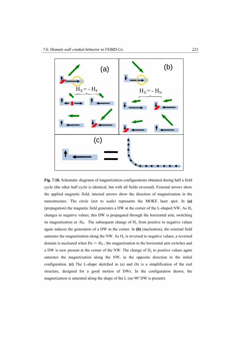
7.6. Domain wall conduit behavior in FEBID-Co 221
Fig. 7.18. Schematic diagrams of magnetization configurations obtained during half a field
cycle (the other half cycle is identical, but with all fields reversed). External arrows show
the applied magnetic field; internal arrows show the direction of magnetization in the
nanostructure. The circle (not to scale) represents the MOKE laser spot. In (a)
(propagation) the magnetic field generates a DW at the corner of the L-shaped NW. As Hx
changes to negative values, this DW is propagated through the horizontal arm, switching
its magnetization at -HP. The subsequent change of Hy from positive to negative values
again induces the generation of a DW in the corner. In (b) (nucleation), the external field
saturates the magnetization along the NW. As Hx is reversed to negative values, a reversed
domain is nucleated when Hx =- HN ; the magnetization in the horizontal arm switches and
a DW is now present at the corner of the NW. The change of Hy to positive values again
saturates the magnetization along the NW, in the opposite direction to the initial
configuration. (c) The L-shape sketched in (a) and (b) is a simplification of the real
structure, designed for a good motion of DWs. In the configuration drawn, the
magnetization is saturated along the shape of the L (no 90º DW is present).
(a)
HX = - HP
(b)
HX = - HN
(c)
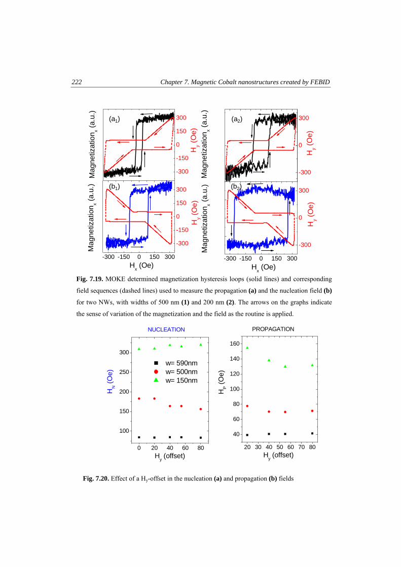
222 Chapter 7. Magnetic Cobalt nanostructures created by FEBID
Fig. 7.20. Effect of a Hy-offset in the nucleation (a) and propagation (b) fields
20 30 40 50 60 70 80
40
60
80
100
120
140
160
0 20 40 60 80
100
150
200
250
300
HP (O
e)
w= 590nm w= 500nm w= 150nm
NUCLEATION
Hy (offset)
HN (O
e)
Hy (offset)
PROPAGATION
Fig. 7.19. MOKE determined magnetization hysteresis loops (solid lines) and corresponding
field sequences (dashed lines) used to measure the propagation (a) and the nucleation field (b)
for two NWs, with widths of 500 nm (1) and 200 nm (2). The arrows on the graphs indicate
the sense of variation of the magnetization and the field as the routine is applied.
-300 -150 0 150 300
-300
0
300
-300
0
300
Hy (O
e)
Mag
netiz
atio
n x (a.u
.)M
agne
tizat
ion x (a
.u.)
Hy (O
e)
Hx (Oe)
-300 -150 0 150 300
-300
-150
0
150
300
-300
-150
0
150
300
Hy (
Oe)
Mag
netiz
atio
n x (a.u
.)M
agne
tizat
ion x (a
.u.)
Hy (O
e)
Hx (Oe)
(a2)
(b2)
(a1)
(b1)
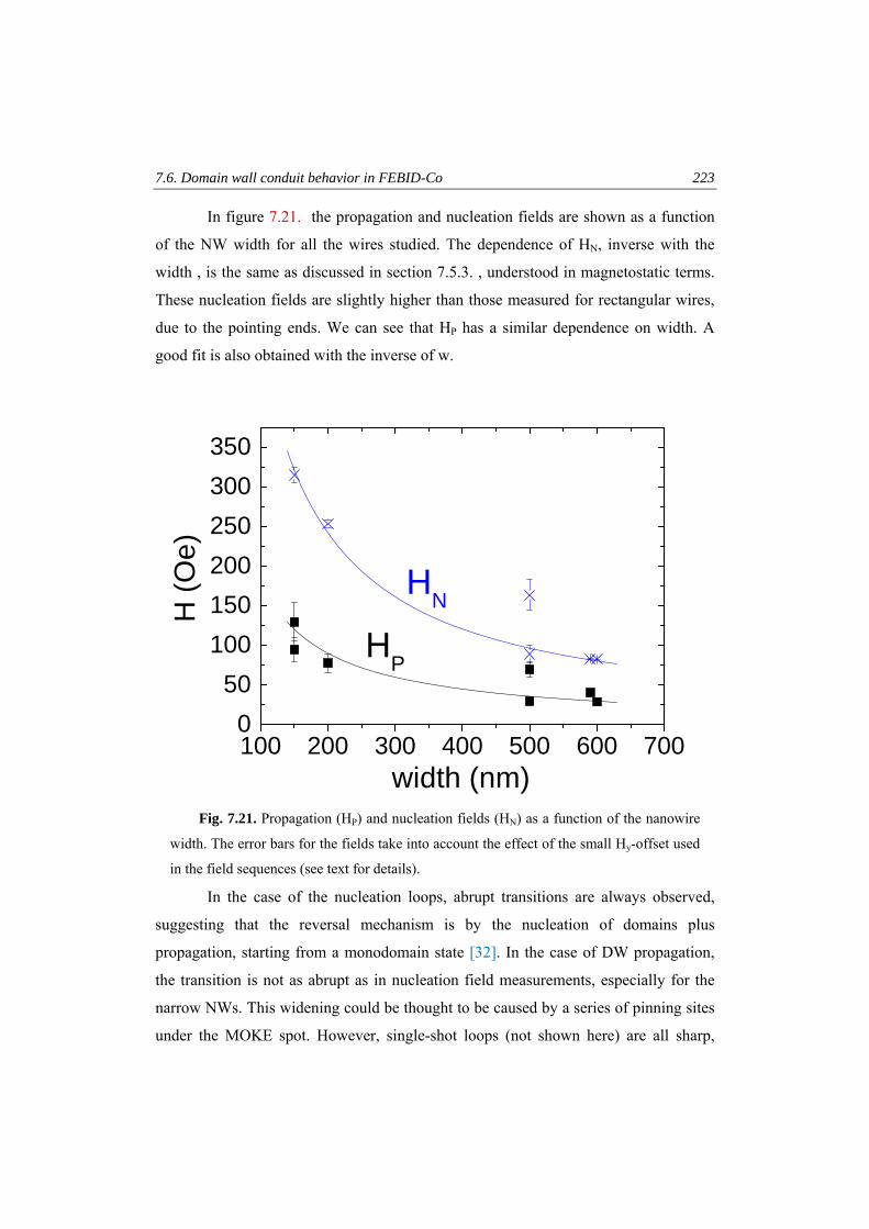
7.6. Domain wall conduit behavior in FEBID-Co 223
In figure 7.21. the propagation and nucleation fields are shown as a function
of the NW width for all the wires studied. The dependence of HN, inverse with the
width , is the same as discussed in section 7.5.3. , understood in magnetostatic terms.
These nucleation fields are slightly higher than those measured for rectangular wires,
due to the pointing ends. We can see that HP has a similar dependence on width. A
good fit is also obtained with the inverse of w.
In the case of the nucleation loops, abrupt transitions are always observed,
suggesting that the reversal mechanism is by the nucleation of domains plus
propagation, starting from a monodomain state [32]. In the case of DW propagation,
the transition is not as abrupt as in nucleation field measurements, especially for the
narrow NWs. This widening could be thought to be caused by a series of pinning sites
under the MOKE spot. However, single-shot loops (not shown here) are all sharp,
100 200 300 400 500 600 7000
50100150200250300350
H (O
e)
width (nm)
HN
HP
Fig. 7.21. Propagation (HP) and nucleation fields (HN) as a function of the nanowire
width. The error bars for the fields take into account the effect of the small Hy-offset used
in the field sequences (see text for details).
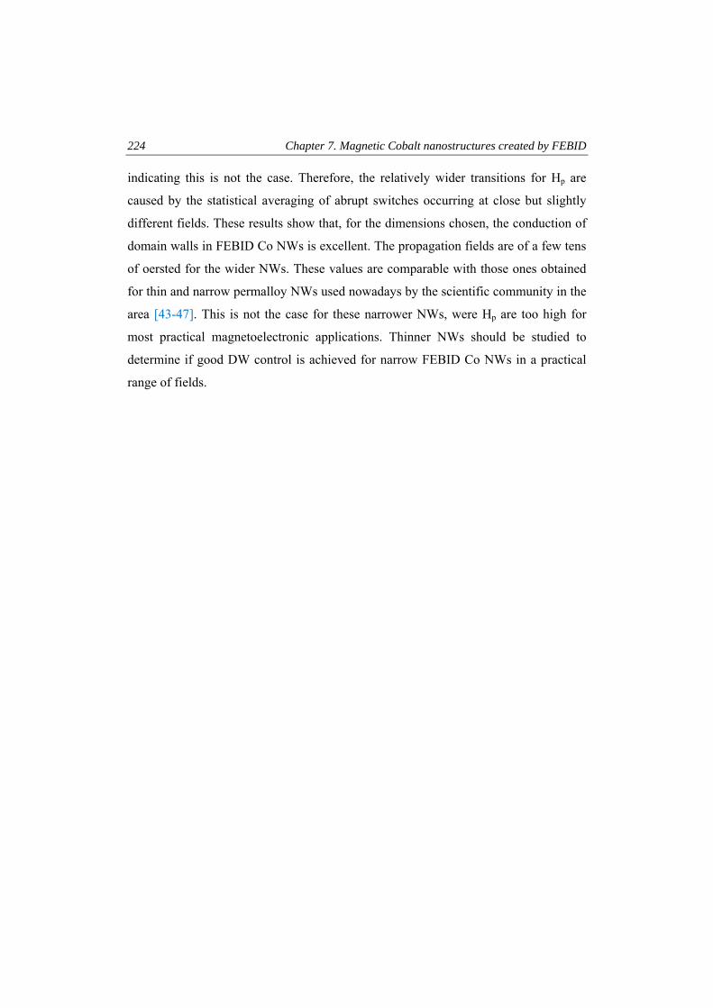
224 Chapter 7. Magnetic Cobalt nanostructures created by FEBID
indicating this is not the case. Therefore, the relatively wider transitions for Hp are
caused by the statistical averaging of abrupt switches occurring at close but slightly
different fields. These results show that, for the dimensions chosen, the conduction of
domain walls in FEBID Co NWs is excellent. The propagation fields are of a few tens
of oersted for the wider NWs. These values are comparable with those ones obtained
for thin and narrow permalloy NWs used nowadays by the scientific community in the
area [43-47]. This is not the case for these narrower NWs, were Hp are too high for
most practical magnetoelectronic applications. Thinner NWs should be studied to
determine if good DW control is achieved for narrow FEBID Co NWs in a practical
range of fields.
7.7. Conclusions 225
7.7. Conclusions
We have done a complete characterization of the compositional,
microstructural and magnetotransport properties of FEBID-Co nanowires. EDX
measurements show Co percentages higher than 90% in deposits grown under high
beam currents, with percentages around 80% for low currents. We explain the
evolution of composition, as well as the high purity attained, in terms of the high local
heating induced by the Field-Emission Gun Beam. HRTEM images show that FEBID-
Co is polycrystalline, with grain sizes ~2-5 nm. For high currents, Hall, Planar Hall
effect and MR are the typical ones for polycrystalline cobalt, with metallic conduction.
From these measurements we infer a saturation magnetization very close to the bulk
value. NWs grown under low currents show degraded magnetotransport properties.
We report direct hysteresis loop measurements performed by MOKE on single
Co nanowires fabricated by FEBID. We have done a systematic study of the reversal
of the magnetization in cobalt wires grown by FEBID in a wide range of dimensions.
The magneto-optical signal of the grown structures is high for all beam currents,
giving account of the magnetic character of the FEBID-Co under the chosen
conditions. The coercive field is proportional to the thickness/width ratio, indicating
that the differences in the coercivity with dimensions are ruled by the magnetostatic
energy. For high aspect ratios, the shape anisotropy forces the magnetization to lie in
the longitudinal direction of the NW in remanence.
By the creation of L-shaped NWs, and the application of 2-directions in-plane
magnetic field routines, we have demonstrated well-controlled formation and motion
of DWs in cobalt FEBID NWs. In the range of dimensions studied, the process for
reversal of the NW is well controlled by the magnetic fields applied, being possible to
select either DW propagation, or nucleation of a new domain. Both kinds of processes
occur at well-defined fields. Significant differences are found for the fields necessary
to reverse the magnetization, if a DW is initially present, or not, in the nanostructure.
This demonstrates the conduit properties of the Co FEBID nanowires.
226 Chapter 7. Magnetic Cobalt nanostructures created by FEBID
The excellent results obtained for FEBID-Co, makes this technique very
attractive for future applications. Implementation of complex magnetic NW networks,
necessary for real applications based on DW control, is a routine task with this
technique, with the enormous advantage of the simplicity with respect to others with
nanometer resolution, and the possibility to create these devices, in principle, on any
surface. Moreover, the good performances of FEBID for creating 3d-structures, makes
this technique a unique tool for the fabrication of magnetic nanostructures.
Chapter 8
Conclusions and outlook
The work carried out throughout this Doctoral thesis concerns the study of
electrical and magnetic properties in several nanometric materials, with different range
of scales: thin films, atomic-sized nanoconstrictions, and micro and nanowires. In this
chapter the main conclusions of the work are summarized, as well as future
perspectives resulting from this work. General conclusions, especially regarding the
use of experimental techniques and methods will be first shown. Secondly, the
concrete conclusions of the three general subjects of the thesis will be exposed: Fe3O4
thin films, nanoconstrictions created by FIB and nanowires created by FEBID/FIBID.
228 Chapter 8. Conclusions and outlook
8.1. General conclusions
The Doctoral thesis has been done thanks to the synergy of two research
institutes in Zaragoza: The (mixed CSIC-University of Zaragoza) Institute of
Materials Science of Aragón (ICMA), with a long and reputed experience in the
materials science research, and the (University of Zaragoza) Institute of Nanoscience
of Aragón (INA), interdisciplinary institute which holds state of the art equipments in
the Nanoscience field. This is the first thesis defended in this region where top-down
micro and nanolithography techniques using equipments of Zaragoza Institutions have
been used. Novel methods and procedures have been developed, which will serve as a
useful input for further research in our institutes regarding nanoscale materials and
devices. I should specially mention the development of some photolithography and
nanolithography processes, which require the learning of a large amount of
experimental techniques and protocols. Besides, the assembly and control of
equipment for the study of magnetotransport properties has been carried out. Finally,
some successful procedures for the control of the resistance of devices while they are
being manipulated in a Dual Beam equipment are also innovative in this work, even
pioneer at the international level.
8.1. Fe3O4 epitaxial thin films 229
8.2. Fe3O4 epitaxial thin films
Due to the high spin polarization of Fe3O4, with potential applications in
Spintronics devices, magnetotransport properties in epitaxial Fe3O4 thin films grown
on MgO (001) have been thoroughly studied. The photolithography process performed
has permitted us to study the longitudinal and transversal components of the resistivity
tensor in a wide range of temperatures, above and quite deep below the Verwey
transition.
Resistivity and magnetoresistance measurements reproduce previous results in
the literature, supporting the epitaxial character of the films. The transport properties
of the ultra-thin films are highly dominated by the scattering produced in the antiphase
boundaries. This is also evidenced in the systematic study of the Planar Hall effect,
giving a record value for the PHE at room temperature. Below the Verwey transition,
colossal values never attained before in any material, in the mΩcm range, are
measured. The changes in the AMR sign below the transition, as well as the
dependence of its magnitude with temperature are not well understood yet.
An important experimental result has been obtained regarding the study of the
Anomalous Hall effect, in four orders of magnitude of the longitudinal conductivity.
The dependence σH ∝ σxx1.6 is fulfilled in all cases, with no influence of the mechanism
responsible for conduction, different degree of scattering at the APBs, etc. This is a
universal behavior of all magnetite results reported in literature, as well as of all
compounds in the dirty regime of conductivities. In our opinion, deeper theoretical
work should be done to clear out how the model predicting this behavior fits with non-
metallic conduction.
The first magnetic tunnel junction based on Fe3O4 electrodes with MgO
barrier are currently (2009) being grown in our laboratory by J. Orna. We hope that
the experience gained in this thesis on the magnetotransport properties and
photolithography process of Fe3O4 films will contribute to the successful development
of these challenging devices in Zaragoza.
230 Chapter 8. Conclusions and outlook
8.3. Creation of atomic-sized constrictions in metals using a Focused-Ion-Beam
We have developed a novel method to fabricate controlled atomic-sized
constrictions in metals, by measuring the conduction of the device while a Focused-
Ion-Beam etching process is being done. We have demonstrated that the technique
works when using Cr and Fe, creating stable atomic-sized constrictions under vacuum
inside the same chamber. This method has two main advantages with respect to more
conventional (STM, MBJ, EBJ, etc) procedures. First, the FIB processes can be
introduced in the standard protocols for the integrated circuits industry, so possible
applications of these devices would be feasible using this methodology, which is not
the case for the others. Second, regarding atomic-sized in contacts in magnetic
materials, where huge magnetoresistance effects observed in the literature are under
debate, we consider that the good adherence of the atoms forming the contact to a
substrate can minimize artefacts, making this technique more suitable for this kind of
studies.
The stability of the contacts when exposed to ambient conditions has been
evidenced in iron nanoconstrictions. The results obtained are not systematic, although
there is no doubt about the preservation of the magnetic character of the material after
ion irradiation in some of the devices. The promising results for samples in the
tunnelling regime of conduction constitutes a promising filed for the study of BMR
and BAMR. New strategies for protection of the constrictions, together with the
possibility to implement a device for magnetic measurements attached to the FIB
chamber, to avoid the exposure of the sample to air, would be substantial advances for
this research.
The method developed is now being successfully applied in our laboratory for
other types of materials, with high interest from a fundamental and applied point of
view.
8.3. Nanowires created by Focused Electron/Ion Beam Induced Deposition 231
8.4. Nanowires created by Focused Electron/Ion Beam Induced Deposition
An important part of the thesis has been devoted to the study of nanowires
created by these promising nanolithography techniques. The work has been done with
three types of gas precursors: (CH3)3Pt(CpCH3), W(CO)6 and Co2(CO)8, and using in
the first case both focused electrons and ions to dissociate the precursor molecules,
using ions in the second case, and using electrons in the third one. In such local
deposition, the material is in general composed of a mixture of carbon and metal. This
wide work allows having a general view of the complex physical phenomena under
these processes, which produce completely different microstructures in the material.
With the (CH3)3Pt(CpCH3) precursor, an amorphous carbon matrix with nanometric
platinum clusters embedded inside is produced. With W(CO)6, an amorphous
disordered carbon-tungsten microstructure is formed, whereas using Co2(CO)8, under
high currents, almost pure polycrystalline cobalt is grown. Several physical
phenomena have been studied in each case, all of them influenced by the particular
microstructure of the material.
In the case of Pt-C nanowires, we have observed a Mott-Anderson metal-
insulator transition as a function of the carbon/metal concentration. This explains, in
principle, contradictory results in the literature up to now. This work shows the
importance of tuning the parameters in a FEBID/FIBID process, since in this case
insulator or metallic nanowires can be created. The discovery of an exponential
decrease in the conductance for the most resistive samples demonstrates the validity of
the theories for hopping under strong electric fields in a nanometric structure. The
method for controlling the resistance as the deposit is being performed, analogous to
that for constrictions, has been evidenced to be very useful, and is now of general use
in our laboratory.
By the study of the low temperature electrical properties of FIBID-W micro
and nanowires, we have determined that wires with sub-100nm lateral width retain the
superconducting properties. This, together with the outstanding properties of this
material, as determined by Scanning-Tunneling-Spectroscopy measurements in the
232 Chapter 8. Conclusions and outlook
group of Prof. Sebastián Viera, make FIBID-W a promising nanoscale
superconductor. Nano-SQUIDS and Andreev reflection nanocontacts based on this
nanodeposit are some promising applications currently developed in our group.
By the use of moderately high beam currents, FEBID-Co deposits (nanowires
and nanostructures) were obtained, reaching the highest, up to now, metallic purity of
the 90%. As a result, magnetotransport measurements in Co nanowires deposited in
these conditions are similar to those of pure Co wires fabricated by conventional
nanolithography techniques. When using low currents, the degradation of these
properties was observed. By the use of spatially-resolved longitudinal Magneto-
Optical-Kerr-effect, we have studied hysteresis loops in single wires with different
aspect ratios. The coercive field is linear with the thickness/width ratio, indicating that
the magnetostatic energy dominates the configuration of the magnetization in the
wires. For high aspect ratios, the shape anisotropy forces the remanent magnetization
to lie in the longitudinal direction of the NW. By creating L-shaped nanowires, and
using two-dimensional field routines, we have demonstrated the good domain wall
conduit behavior of this material. The unique advantages of this technique for creating
3-dimensional nanostructures make this result especially interesting. Steps in this
direction are in progress. Besides, next steps should be given by performing
experiments where the magnetization is switched by a spin-torque effect, and not by
an external magnetic field.
Following works should, in general, be devoted to the study of the resolution
limits of these techniques, and determine how their functional properties are affected
when the sizes are reduced substantially. Another important aspect is to try to obtain
purely metallic nanostructures, of interest in nanoelectronics. Further functionality of
these deposits in a wide variety of applications is strongly desired. Finally, the
combination of these materials to create hybrid devices such as
magnetic/superconducting ones, together with the good control of the resistance, can
imply the study of fascinating phenomena.
Bibliography
Chapter 1: Introduction
[1] R.P. Feynman, Engineering and Science, Caltech, February (1960)
[2] C.M. Vest, dissertation in Massachusetts Institute of Technology (2005)
[3] S. Bensasson, Technology roadmap for nanoelectronics (2000)
[4] G. Moore, Electronics 5, 114 (1965)
[5] http://web.sfc.keio.ac.jp
[6] J. Ferrer, and V.M. García-Suárez, J. Mater. Chem.19, 1696 (2009)
[7] L.R. Harriott, IEEE Proceedings (2001)
[8] T. Ito, and S. Okazak, Nature 406, 1027 (2000)
[9] The name of the technology means that the channel joining the source and drain in transistor has this size. In this case 45 nm.
[10] R. Chau, B. Doyle, S. Datta, J. Kavalieros, and K. Zhang, Nat. Mat. 6, 810 (2007)
[11] A. Correira, and P.A Serena, “Nanociencia y Nanotecnología en España”, Fundación Phantoms, 7 (2008)
[12] É. du Trémolet de Laceisserie, D. Gignoux, and M. Schlenker, “Magnetism”, Vol. 2 (“Materials and applications”), chapter 21, 305 Springer (2005)
[13] MRS bulletin 31, May 2006
[14] E.E. Fullerton, SNOW School, Nancy (France), 2008
[15] P. Grünberg, R. Schreiber, Y. Pang, M.B. Brodsky and H. Sowers, Phys. Rev. Lett. 57, 2442 (1986)
[16] M.T. Béal-Monod, Phys. Rev. B 36, 8835 (1987)
[17] N. Mott, Adv. Phys. 13, 325 (1964)
[18] A. Fert, and I.A. Campbell, Phys. Rev. Lett. 21, 1190 (1968)
234 Bibliography
[19] C. Chappert, A. Fert, and F. Nguyen Van Dau, Nat. Mat. 6, 813 (2007)
[20] R. Jansen, J. Phys. D: Appl. Phys. 36, R289 (2003)
[21] I. Zutic, J. Fabian, and S. Dasma, Rev. Mod. Phys. 76, 323 (2004)
[22] E.E. Fullerton, and I.K. Schüller, ACS Nano 5, 384 (2007)
[23] A. Fert, Rev. Mod. Phys. 80, 1517 (2008)
[24] P. Grünberg, Rev. Mod. Phys. 80, 1531 (2008)
[25] M.N. Baibich, J.M. Broto, A. Fert, F. Nguyen Van Dau, F. Petroff, P. Etienne, G. Creuzet, A. Friederich, and J. Chazelas, Phys. Rev. Lett. 61, 2472 (1988)
[26] G.P. Binasch, F. Grünberg, F. Saurenbach, and W. Zinn, Phys. Rev. B 39, 4828 (1989)
[27] Classification adapted from J.L. Kosta-Krämers, “Nanociencia y Nanotecnología en España”, Fundación Phantoms, 80 (2008)
[28] K. Roy, K.S. Yeo, “Low Voltage, Low Power VLSI Subsystems”, McGraw-Hill Professional (2004)
[29] D.K. Ferry, Science 319, 579 (2008)
[30] K. Uchida, J. Koga, R. Ohba, and A. Toriumi, Electron Devices Meeting, 2000
[31] G.I. Haddad, P. Mazmuder, and J.N. Schulmanm, IEEE Proceedings 86, 641 (1998)
[32] L. Geppert, IEEE Spectrum 46, September 2000
[33] K.C. Schwab, and M.L. Roukes, Phyics. Today 37, July 2005
[34] F. Su, K. Chakrabarty, and R.B. Fair, IEEE Trans. Design Int. Circ. Sys. 25, 211 (2006)
[35] J. Moodera, L.R. Kinder, R.M. Wong, R. Meservey, Phys. Rev. Lett. 74, 3273 (1995)
(1985)
[36] M. Bowen, M. Bibes, A. Barthélémy, J.P. Contour, A. Anane, Y. Lemaître, A. Fert, Appl. Phys. Lett. 82, 233 (2003)
[37] S. Mao, Y. Chen, F. Liu, X. Chen, B. Xu, P. Lu, M. Patwari, H. Xi, C. Chang, B.
Bibliography 235
Miller, D. Menard, B. Pant, J. Loven, K. Duxstad, S. Li, Z. Zhang, A. Johnston, R. Lamberton, M. Gubbins, T. McLaughlin, J. Gadbois, J. Ding, B. Cross, S. Xue, and P. Ryan, IEEE Trans. Magn. 42, 97 (2006)
[38] J.M. Kikkawa, D.D. Aschwalom, I.P. Smorchkova, N. Samarth, Science 277, 1284 (1997)
[39] P.R. Hammar, B.R. Bennett, M.J. Yang, and M. Johnson, Phys. Rev. Lett. 83, 203 (1999)
[40] H.J. Zhu, M. Ramsteiner, H. Kostial, M. Wassermeier, H.-P. Schönherr, and K.H. Ploog Phys. Rev. Lett. 87, 016601 (2001)
[41] R. Fiederling, M. Keim, G. Reuscher, W. Ossau, G. Schmidt, A. Waag and L.W. Molenkamp, Nature 402, 787 (1999)
[42] S. Datta, and B. Das, Appl. Phys. Lett. 56, 665 (1990)
[43] J. Barnaś, and A. Fert, Phys. Rev. Lett. 80, 1058 (1998)
[44] S. Takahashi, and S. Maekawa, Phys. Rev. Lett. 80, 1758 (1998)
[45] A.R. Rocha, V. M. García-Suárez, S.W. Bailey, J.C. Lambert, J. Ferrer, and S. Sanvito, Nat. Mat. 4, 335 (2005)
[46] Z.H. Xiong, D. Wu, Z.V. Vardeny, and J. Shi, Nature 427, 821 (2004)
[47] A. Riminucci, I. Bergenti, L.E. Hueso, M. Murgia, C. Taliani, Y. Zhan, F. Casoli, M.P. de Jong, V. Dediu, arXiv:cond-mat/0701603v1
[48] T.S. Santos,J.S. Lee, P. Migdal, I.C. Lekshmi, B. Satpati, and J.S. Moodera, Phys. Rev. Lett. 98, 016601 (2007)
[49] L.E. Hueso, J.M. Pruneda, V. Ferrari, G. Burnell, J.P. Valdés-Herrera, B.D. Simons, P.B. Littlewood, E. Artacho, A. Fert, N.D. Mathur, Nature 445, 410 (2007)
[50] E.W. Hill, A.K. Geim, K. Novoselov, F. Schedin, P. Blake, IEEE Trans. Magn. 42, 2694 (2006)
[51] R. Allenspach, and P.-O. Jubert, MRS bulletin 31, 395 (2006)
[52] R.P. Cowburn, J. Phys. D.: Appl. Phys. 33, R1 (2000)
[53] T. Ono, H. Muyajima, K. Sigheto, K. Mibu, N. Hosoito, and T. Shinjo, Science 284, 468 (1999)
236 Bibliography
[54] S.S.P. Parkin, M. Hayashi, and L. Thomas, Science 320, 190 (2008)
[55] D.A. Allwood, G. Xiong, C.C. Faulkner, D. Atkinson, D. Petit, R.P. Cowburn, Science 309, 1688 (2005)
[56] V. S. Pribiag, I. N. Krivorotov, G. D. Fuchs, P. M. Braganca, O. Ozatay, J. C. Sankey, D. C. Ralph, R. A. Buhrman, Nature Phys. 3, 498 (2007)
[57] M. Weigand, B. Van Waeyenberge, A. Vansteenkiste, M. Curcic,V. Sackmann, H. Stoll, T. Tyliszczak, K. Kaznatcheev, D. Bertwistle, G. Woltersdorf, C.H. Back, and G. Schütz, Phys. Rev. Lett. 102, 077201 (2009)
[58] M. R. Freeman and B. C. Choi, Science 294, 1484 (2001)
[59] L. Berger, J. Appl. Phys. 3, 2156 (1978)
[60] P.P. Freitas, L. Berger, J. Appl. Phys. 57, 1266 (1985)
[61] D.C. Ralph, and M.D. Stiles, J. Magn. Magn. Mat. 320, 1190 (2008)
[62] J.A. Katine, F.J. Albert, R.A. Buhrman, E. B. Myers, and D. C. Ralph, Phys. Rev. Lett. 84, 3149 (2000)
[63] J. Grollier, V. Cros, A. Hamzic, J.M. George, H. Jaffrès, A. Fert, G. Faini, J. Ben Youssef, and H. Legall, Appl. Phys. Lett. 8, 3663 (2001)
[64] C. Chappert, A. Fert, F. Van dau, Nature Mat. 6, 813 (2006)
[65] S.I. Kiselev, J.C. Sankey, I.N. Krivorotov, N.C. Emley, R.J. Schoelkopf, R.A. Buhrman, and D.C. Ralph, Nature (London) 425, 308 (2003)
[66] W. H. Rippard, M.R. Pufall, S. Kaka, S.E. Russek, and T. J. Silva, Phys. Rev. Lett. 92, 027201 (2004)
[67] N. Vernier, D.A. Allwood, D. Atkinson, M.D. Cooke and R.P. Cowburn, Europhys. Lett., 65(4),526 (2004)
[68] N. Grobert, Materials Today 10, 28 (2007)
[69] M.P. Anantram, and F.L. Leonard, Rep. Prog. Phys. 69, 507 (2006)
[70] N. Agraït, A.L. Yeyati, and J.M. Van Ruitenbeek, Phys. Rep. 377, 81 (2003)
[71] A. Yu. Kasumov, K. Tsukagoshi, M. Kawamura, T. Kobayashi, Y. Aoyagi, K. Senba, T. Kodama, H. Nishikawa, I. Ikemoto, K. Kikuchi, V. T. Volkov, Yu. A. Kasumov, R. Deblock, S. Guéron, and H. Bouchiat, Phys. Rev. B 72, 033414 (2005)
Bibliography 237
[72] A.K. Goel, IEEE 2008
[73] M. Forshaw, R. Stadler, D. Crawley, and K Nikolíc, Nanotechnology 15, S220 (2004)
[74] A. Steane Rep. Prog. Phys. 61, 117 (1998)
[75] A. Galindo and M.A. Martín-Delgado, Rev. Mod. Phys. 74, 347 (2002)
[76] K.K. Berggren, IEEE proceedings 98, 1630 (2004)
[77] A.T. Dorsey, Nature 408, 783 (2000)
[78] A. J. Leggett, Science 296, 861 (2002)
[79] M.A. Sillanpää, I. Park, and Raymond W. Simmonds Nature 449, 438 (2007)
Chapter 2: Experimental techniques
[1] For details of the growth process: [email protected]
[2] LR Harriott, IEEE Proceedings (2001)
[3] T. Ito, and S. Okazak, Nature 406, 1027 (2000)
[4] H.J. Levinson, “Principles of Lithography”, SPIE Press, 2nd edition (2005)
[5] Handbook of Microlithography, Micromachining, and Microfabrication, Volume 2, SPIE Press (1997)
[6] L. Gianuzzi, and F. Stevie, Introduction to Focused Ion Beams: Instrumentation, techniques, theory and practices, Springer Science+ Business Media, Boston (2005)
[7] J. Orloff, M. Utlaut, and L. Swanson, High Resolution Focused Ion Beams: FIB and Its
Applications, Kluwer Academic/Plenum Publishers, NY (2003)
[8] S. Matsui and Y. Ochiai, Nanotechnology 7, 247 (1996)
[9] W. Li, and P.A. Warburton, Nanotechnology 18, 485305 (2007)
[10] A. De Marco, and J. Melngailis, Solid State Electronics 48, 481833 (2004)
238 Bibliography
[11] G.C. Gazzadi and S. Frabboni, J. Vac. Sci. Technol. B 23, L1 (2005)
[12] A. Romano-Rodriguez, and F. Hernández-Ramirez, Microelectron. Eng., 84, 789 (2007)
[13] I. Utke, P. Hoffmann, R. Berger, L. Scandella, Appl. Phys. Lett., 80, 4792 (2002)
[14] E.S. Sadki, S. Ooi, K. Hirata, Appl. Phys. Lett., 85, 6206 (2004)
[15] N. Silvis-Clividjan, C.W. Hagen, and P. Kruit, J. Appl. Phys., 98, 084905, (2005)
[16] I. Utke, P. Hoffmann, and J. Melngailis, J. Vac. Sci. Technol. B 26, 1197 (2008)
[17] W.F. van Dorp, and C.W. Hagen, J. Appl. Phys. 104, 081301 (2008)
[18] A. Botman, J.J. Mulders, R. Weemaes, and S. Mentik, Nanotechnology 17, 3779 (2006)
[19] R.M. Langford, T.–X. Wang, and D. Ozkaya, Micr. Eng. 84, 748 (2007)
[20] R.P. Cowburn, D.K. Koltsov, A.O. Adeyeye, and M.E. Welland, Appl. Phys. Lett. 73, 3947 (1998)
[21] D.A. Alwood, G. Xiong, M.D. Cooke, and R.P. Cowburn, J. Phys. D.: Appl. Phys. 36, 2175 (2003)
Chapter 3: Magnetotransport properties in epitaxial Fe3O4 thin films
[1] M.L. Glasser, and F.J. Milford, Phys. Rev. 130, 1783 (1963)
[2] E.J.W. Verwey, Nature (London) 144, 327 (1939)
[3] F. Walz, J. Phys.: Condens. Matter 14, R285 (2002)
[4] J. García and G. Subías. J. Phys.: Condens. Matter 16, R145 (2004)
[5] D. Ihle, and B. Lorenz, J. Phys. C: Solid State Phys. 18 L647 (1985)
[6] N.F. Mott, Metal–Insulator Transitions 2nd edn (London: Taylor and Francis) (1990)
[7] A. Yanase and K. Siratori, J. Phys. Soc. Jpn. 53, 312 (1984
[8] Z. Zhang, and S. Satpathy, Phys. Rev. B 44, 13319 (1991)
Bibliography 239
[9] S.F. Alvarado, W. Eib, F. Meier, D.T. Pierce, K. Sattler, and H.C. Siegmann, Phys. Rev. Lett. 34, 319 (1975)
[10] M. Fonin, Yu S. Dedkov, R. Pentcheva, U Rüdiger, and G. Güntherodt, J. Phys.: Condens. Matter 19, 315217 (2007)
[11] G. Hu, and Y. Suzuki, Phys. Rev. Lett. 89, 276601 (2002)
[12] J.Y.T. Wei, N.-C. Yeh, R.P. Vasquez, A. Gupta, J. Appl. Phys. 83, 7366 (1998)
[13] M. Jullière, Phys. Lett. 74, 3273 (1975)
[14] J.M. De Teresa, A. Barthélèmy, A. Fert, J.P. Contour, , R. Lyonnet, F. Montaigne, and P. Seneor, Science 286, 507 (1999)
[15] W.H. Butler, X.G. Zhang, T.C. Schulthess, and J.M. MacLaren. Phys. Rev. B 63, 054416 (2001)
[16] S Yuasa, and D.D. Djayaprawira, J. Phys.D: Appl. Phys. 40, R337 (2007)
[17] W.E. Picket, and J.S. Moodera, Phys. Today 54(5), 39 (2001)
[18] C.M. Fang, G. A. de Wijs, and R. A. de Groot, J. Appl. Phys. 91, 8340 (2002)
[19] D. Reisinger, P. Majewski, M.Opel, L. Alff, and R. Gross, Appl. Phys. Lett. 85, 4980 (2004)
[20] A.V. Ramos, J.-B. Mouse, M.-J. Guittet, A.M. Bataille, M. Gautier-Soyer, M. Viret, C. Gatel and P. Bayle- Guillemaud, and E. Snoeck, J. Appl. Phys. 100, 103902 (2006)
[21] W. Eerestein, T.T. M. Palstra, T. Hibma, and S. Celotto, Phys. Rev. B 66, 201101(R) (2002)
[22] S. K. Arora, R. G. S. Sofin, I. V. Shvets, and M. Luysberg, J. Appl. Phys. 100, 073908 (2006)
[23] Y. Zhu, and J.W. Cai, Appl. Phys. Lett. 90, 012104 (2007)
[24] J.F. Bobo, D. Basso, E. Snoeck, C. Gatel, D. Hrabovsky, J.L. Gauffier, L. Ressier, R. Mamy, S. Vinsnovsky, J. Hamrle, J. Teillet, and A.R. Fert, Eur. Phys. J. B 24, 43 (2001)
[25] G.Q. Gong, A. Gupta, G. Xiao, W. Qian, and V.P. Dravid, Phys. Rev. B 56, 5096 (1997)
[26] M. Ziese, and H.J. Blythe, J. Phys. Condens. Matter 12, 13 (2000)
240 Bibliography
[27] D.T. Margulies, F.T. Parker, M. L. Rudee F.E. Spada, J. N. Chapman, P. R. Aitchison, and A.E. Berkowitz, Phys. Rev. Lett 79, 5162 (1997)
[28] W. Eerenstein, T.T.M. Palstra, S.S. Saxena, and T. Hibma, Phys. Rev. Lett. 88, 247204 (2002)
[29] D.J. Huang, C.F. Changa, J. Chena, L.H. Tjengc, A.D. Ratad, W.P. Wua, S.C. Chunga, H.J. Lina, T. Hibmad, and C. T. Chen, J. Magn. Magn. Mat. 239, 261 (2002)
[30] D. Serrate, J.M. De Teresa, P.A. Algarabel, R. Fernández-Pacheco, M.R. Ibarra, J. Galibert, J. Appl. Phys. 97, 084322 (2005)
[31] This piece of work forms part of the thesis of Julia Orna (University of Zaragoza): [email protected]
[32] L.J. van der Pauw, Philips Technical Review 36, 220 (1958)
[33] The TEM work was done by César Magén ([email protected]) and Ettiene Snoeck in the CEMES-CNRS laboratory in Toulouse (France)
[34] X.W. Li, A. Gupta, Gang Xiao, G.Q. Gong, J. Appl. Phys. 83, 7049 (1998)
[35] J.P. Wright, J.P. Attfield, and P.G. Radaelli, Phys. Rev. Lett. 87, 266401 (2001)
[36] W. Eerenstein, T. Hibma, and S. Celotto, Phys. Rev. B 70, 184404 (2004)
[37] J. Kondo, Prog. Theor. Phys. 27, 772 (1962)
[38] V.V. Gridin, G.R. Hearne, and J.M. Honing, Phys. Rev. B 53, 15518 (1996)
[39] J.S-Y. Feng, R.D. Pashley, and M-A Nicolet, J. Phys. C: Sol. State Phys. 8, 1010 (1975)
[40] I.A. Campbell, and A. Fert, Magnetic Materials 3 747 (1982)
[41] G. Li , T. Yang, Q. Hu, H. Jiang, and W. Lai, Phys. Rev. B 65, 134421 (2002)
[42] S.T.B. Goennenwein, R.S. Keizer, S.W. Schink, I. van Dijk, T.M. Klapwijk, G. X. Miao, G. Xiao, and A. Gupta, Appl. Phys. Lett. 90, 142509 (2007)
[43] A. Schuhl, F. Nguyen Van Dau, and J.R. Childress, Appl. Phys. Lett. 66, 2751 (1995)
[44] A.O. Adeyeye, M.T. Win, T.A. Tan, G.S. Chong, V.Ng, T.S. Low, Sensors and Actuators A 116, 95 (2004)
Bibliography 241
[45] H.X. Tang, R.K. Kawakami, D.D. Awschalom, and M.L. Roukes, Phys. Rev. Lett 90, 107201 (2003)
[46] K.Y. Wang, K.W. Edmonds, R.P. Camion, L.X. Zhao, C.T. Foxon, and B.L. Gallagher, Phys. Rev. B 72, 085201 (2005)
[47] W.L. Lim, X. Liu, K. Dziatkowski, Z. Ge, S. Shen, J.K. Furdyna, and M. Dobrowolska, J. Appl. Phys. 99, 08D505 (2006)
[48] D.Y. Shin, S.J. Chung, S. Lee, X. Liu, and J.K. Furdyna, Phys. Rev. Lett. 98, 047201 (2007)
[49] H.X. Tang, S. Masmanidis, R.K. Kawakami, D.D. Awschalom, and M.L. Roukes, Nature 43, 52 (2004)
[50] H.X. Tang, and M.L. Roukes, United States Patent 6910382 (2004)
[51] X. Jin, R. Ramos, Y. Zhou, C. McEvoy, I. V. Shvets, J. Appl. Phys. 99, 08C509 (2006)
[52] Y. Bason, L. Klein, H. Q. Wang, J. Hoffman, X. Hong, V. E. Henrich, and C. H. Ahn, J. Appl. Phys. Lett. 101, 09J507 (2007)
[53] Y. Bason, L. Klein, J.-B. Yau, X. Hong, and C. H. Ahn, Appl. Phys. Lett. 84, 2593 (2006)
[54] Y. Bason, L. Klein, J.-B. Yau, X. Hong, J. Hoffman, and C. H. Ahn, J. Appl. Phys. 99, 08R701 (2006)
[55] V. Skumpryev, H.J. Blythe, J. Cullen, J.M.D. Coey, J. Magn. Magn. Mater. 196-197, 515 (1999)
[56] I. Leonov and A.N. Yaresko, J.Phys.: Condens. Matter 19, 021001 (2007)
[57] J. Smit, Physica (Utretch) 21, 877 (1955), 24, 39 (1958)
[58] L. Berger, Phys. Rev. B 2, 4559 (1970)
[59] A. Crepiéux, and P. Bruno, Phys. Rev. B 64, 014416 (2001)
[60] R. Karplus, and J.M. Luttinger, Phys. Rev. 95, 1154 (1954)
[61] G. Sundaram, and Q. Niu, Phys. Rev. B 59, 14915 (1999)
[62] S. Onoda, N. Sugimoto, and N. Nagaosa, Phys. Rev. Lett. 97, 126602 (2006)
[63] T. Miyasato, N.Abe, T.Fujii, A. Asamitsu, S. Onoda, Y. Onose, N. Nagaosa, and
242 Bibliography
Y. Tokura, Phys. Rev. Lett. 99, 086602 (2007)
[64] T. Fukumura, H. Toyosaki, K. Ueno, M. Nakano, T. Yamasaki, and M. Kawasaki, Jpn J. Appl. Phys. 46, 26 (2007) and references therein
[65] Y. Zhu, and J.W. Cai, Appl. Phys. Lett. 90, 012104 (2007)
[66] H. Liu , E. Y. Jiang, R.K. Zheng, and H.L. Bai, J. Phys. : Condens. Matter 15 8003 (2003)
[67] J. Lavine, Phys. Rev. 123, 1273 (1961)
[68] V. Brabers, F. Waltz, and H. Kronmuller, Phys. Rev. B 58, 14163 (1998)
[69] D. Kostopoulos, and A. Theodossiou, Phys. Stat. Sol. (a) 2, 73 (1970)
[70] S. Todo, K. Siratori and S. Kimura, J. Phys. Soc. Jpn. 64, 6 (1995)
[71] Z. Chang, D. Satpathy, Phys Rev. B 44, 13319 (1991)
[72] H. Toyosaki, T. Fukumura, Y. Yamada, K. Nakajima, T. Chikyow, T. Hasegawa, H. Koinuma, and M. Kawasaki, Nat. Mater. 3, 221 (2004)
[73] K. Ueno, T. Fukumura, H. Toyosaki, M. Nakano, and M. Kawasaki, Appl. Phys. Lett. 90, 072103 (2007)
[74] Y. Lyanda-Geller, S.H. Chun, M.B. Salamon, P.M. Goldbart, P.D. Han, Y. Tomioka, A. Asamitsu, and Y. Tokura, Phys. Rev. B 63, 184426 (2001)
[75] P. Matl, N.P. Ong, Y.F. Yan, Y.W. Li, D. Studebaker, T. Baum, and G. Doubinina, Phys. Rev. B 57, 10248 (1998)
[76] Y. Onose and Y. Tokura, Phys. Rev. B 73, 174421 (2006)
[77] N. Manyala, Y. Sidis, J.F. Ditusa, G. Aeppli, D.P. Young, and Z. Fisk, Nat. Mater. 3, 255 (2004)
[78] Y. Tomioka, T. Okuda, Y. Okimoto, R. Kumai, K.-I. Kobayashi, and Y. Tokura, Phys. Rev. B 61, 422 (2000)
[79] R. Mathieu, A. Asamitsu, H. Yamada, K.S. Takahashi, M. Kawasaki, Z. Fang, N. Nagaosa, and Y. Tokura, Phys. Rev. Lett. 93, 016602 (2004)
[80] F. Matsukura, E. Abe, and H. Ohno, J. Appl. Phys. 87, 6442 (2000)
[81] K.W. Edmonds, R.P. Campion, K.-Y. Wang, A.C. Neumann, B.L. Gallagher, C.T. Foxon, and P.C. Main, J. Appl. Phys. 93, 6787 (2003)
Bibliography 243
[82] A. Oiwa, A. Endo, S. Katsumoto, Y. Iye, and H. Ohno, Phys. Rev. B 59, 5826 (1999)
[83] H. Ohno, H. Munekata, T. Penny, S. von Molnar, and L.L. Chang, Phys. Rev. Lett. 68, 2664 (1992)
[84] F. Matsukura, H. Ohno, A. Shen, and Y. Sugawara, Phys. Rev. B 57, R2037 (1998)
[85] D. Chiba, Y. Nishitani, F. Matsukura, and H. Ohno, Appl. Phys. Lett. 90, 122503 (2007)
[86] S.U. Yuldashev, H.C. Jeon, H.S. Im, T.W. Kang, S.H. Lee, and J.K. Furdyna, Phys. Rev. B 70, 193203 (2004)
Chapter 4: Conduction in atomic-sized magnetic metallic constrictions created by FIB
[2] N. Agraït, A. L. Yeyati, and J. M. Van Ruitenbeek, Phys. Rep. 377, 81 (2003)
[3] Yu.V. Sharvin, Sov. Phys.-JETP 21, 655 (1965)
[3] R. Landauer, IBM J. Res. Dev. 1, 223 (1957)
[4] E. Scheer, N. Agraït, J. C. Cuevas, A.L. Yeyati, B. Ludoph, A. Martín-Rodero, G.R. Bollinger, J.M. van Ruitenbeek, and C. Urbina, Nature 394, 154 (1998)
[5] J.M. van Ruitenbeek , A. Alvarez, I. Pineyro, C. Grahmann, P. Joyez, M.H. Devoret, D. Esteve, and C. Urbina, Rev. Sci. Instrum. 67, 108 (1996)
[6] R. Wiesendanger, Scanning Probe Microscopy and Spectroscopy, Cambridge University Press, Cambridge, 1994.
[7] H. Park, A.K.L. Lim, A.P. Alivisatos, J. Park, and P.L. Mceuen, Appl. Phys. Lett. 75 301 (1999)
[8] A.F. Morpurgo, C.M. Marcus, and D.B. Robinson, Appl. Phys. Lett. 74 2084 (1999)
[9] Schep K M, Kelly P J and Bauer G E W, Phys. Rev. Lett. 74 586 (1995)
[10] N. García, M. Muñoz, and Y. W. Zhao, Phys. Rev. Lett. 82, 2923 (1999)
[12] N. García, M. Muñoz, G.G. Qian, H. Rohrer, I.G. Saveliev, and Y.W. Zhao, Appl. Phys. Lett. 79, 4550 (2001)
244 Bibliography
[13] N. García, G.G. Qiang, and I.G. Saveliev, Appl. Phys. Lett. 80, 1785–7 (2002)
[14] J.J. Versluijs, M.A. Bari, and J.M.D. Coey, Phys. Rev. Lett. 87, 026601 (2001)
[15] S.H. Chung, M. Muñoz, N. García, W.F. Egelhoff, and R.D. Gomez Phys. Rev.Lett. 89, 287203 (2002)
[16] P. Bruno, Phys.Rev. Lett. 83 2425 (1999)
[17] W. F. Egelhoff, Jr., L. Gan, H. Ettedgui, Y. Kadmon, C. J. Powell, P. J. Chen, A. J. Shapiro, R. D. McMichael, J. J. Mallett, T. P. Moffat, and M. D. Stiles, E. B. Svedberg, J. Appl. Phys. 95, 7554 (2004)
[18] M. I. Montero, R. K. Dumas, G. Liu, M. Viret, O. M. Stoll, W. A. A. Macedo, and I.K. Schuller, Phys. Rev. B 70, 184418 (2004)
[19] O. Ozatay, P. Chalsani, N. C. Emley, I. N. Krivorotov, and R. A. Buhrman, J. Appl. Phys. 95, 7315 (2004)
[20] B. Doudin, and M. Viret, J. Phys.: Cond. Matter. 20, 083201 (2008)
[21] N.F. Mott , Proc. R. Soc. A 153, 699 (1936)
[22] J. Smit, Physica 17, 612 (1951)
[23] R. Potter, Phys. Rev. B 10, 4626 (1974)
[24] P. Gambardella, A. Dallmeyer, K. Maiti, M.C. Malagoli, W. Eberhardt, K. Kern, and C. Carbone, Nature 416, 301 (2002)
[25] J. Velev, R. F. Sabirianov, S. S. Jaswal, and E. Y. Tsymbal, Phys. Rev. Lett. 94, 127203 (2005)
[26] D. Jacob, J. Fernández-Rossier, and J. J. Palacios, Phys. Rev. B 77, 165412 (2008)
[27] A. Sokolov, C. Zhang, E. Y. Tsymbal, J. Redepenning, and B. Doudin, Nat. Nanotechnology 2, 171 (2007)
[28] 18. M. Viret, M. Gauberac, F. Ott, C. Fermon, C. Barreteau, G. Autes, and R. Guirado López, Eur. Phys. J. B 51, 1 (2006)
[29] S. –F. Shi, and D. C. Ralph, Nat. Nanotech. 2, 522 (2007)
[30] N. García, C. Hao, L. Yonghua, M. Muñoz, Y. Chen, Z. Cui, Z. Lu, Y. Zhou, G. Pan, A.A. Pasa, Appl. Phys. Lett. 89, 083112 (2006)
Bibliography 245
[31] P. Krzysteczko, and G. Dumpich, Phys. Rev. B 77, 144422 (2008).
[32] T. Huang, K. Perzlaimer, and C.H. Back, Phys. Rev. B 79, 024414 (2009)
[33] O. Céspedes, S.M. Watts, J.M. Coey,K. Dörr, and M. Ziese, Appl. Phys. Lett. 87, 083102 (2005)
[34] S. Khizroev, Y. Hijazi, R. Chomko, S. Mukherjee, R. Chantell. X. Wu, R. Carley, abd D. Litvinov, Appl. Phys. Lett. 86, 042502 (2005)
[35] I. V. Roshchin, J. Yu, A.D. Kent, G.W. Stupian, and M.S. Leung, IEEE. Trans. Magn. Mat. 37, 2101 (2001)
[36] C. Sirvent, J.G. Rodrigo, S. Vieira, N. JurczyszynMingo, and F. Flores, Phys. Rev. B 53 16086 (1996)
[37] J.J. Palacios, A.J. Pérez-Jiménez, E. Louis, E. SanFabián, and J.A. Vergués, Phys. Rev. B 66, 035322 (2002)
[38] A. Hasmy A, A.J. Pérez-Jiménez, J.J. Palacios, P. García-Mochales, J.L. Costa-Kramers, M. Díaz, E. Medina, and P.A. Serena, Phys. Rev. B 72 245405 (2005)
[39] F. Pauly, M. Dreher, J.K. Viljas, M. Häfner, J.C. Cuevas, and P. Nielaba, Phys. Rev. B 74 235106 (2006)
[40] D.R. Strachan, D.E. Johnston, B.S. Guitom, S.S. Datta, P.K. Davies, D.A. Bonell, and A.T.C. Johnson, Phys. Rev. Lett. 100 056805 (2008)
[41] L. Giannuzzi L, and F.A. Stevie, Introduction to Focused Ion Beams: Instrumentation, techniques, theory and practices, Springer Science+Business Media, Boston (2005)
[42] J.G. Simmons, J. Appl. Phys. 34, 1793 (1963)
[43] H.B. Michaelson, J. Appl. Phys. 48, 4729 (1977)
[44] See chapter 5, section 5.2. for details
[45] J.S. Moodera, and G. Mathon, J. Magn. Mag. Mat 200, 248 (1999)
[46] J.V. Oboňa , J.M. de Teresa, R. Córdoba, A. Fernández-Pacheco, M.R. Ibarra, Micr. Eng. 86, 639 (2009)
246 Bibliography
Chapter 5: Pt-C nanowires created by FIBID and FEBID
[1] L. Peñate-Quesada, J. Mitra, and P. Dawson, Nanotech. 18, 215203 (2007)
[2] R. M. Langford, T. –X. Wang, and D. Ozkaya, Micr. Eng. 84, 748 (2007)
[3] J-F. Lin, J.P. Bird, L. Rotkina, and P.A. Bennett, Appl. Phys. Lett., 82, 802 (2003)
[4] J-F. Lin, J.P. Bird, L. Rotkina, A. Sergeev, and V. Mitin, Appl. Phys. Lett. 84, 3828 (2004)
[5] J-F. Lin, L. Rotkina J.P. Bird, A. Sergeev, and V. Mitin , IPAP Conf. Series 5, 17 (2004)
[6] T. Tao, J. Ro, and J. Melngailis, J. Vac. Sci Technol. B 8, 1826 (1990)
[7] J. Puretz, and L. W. Sawson, J. Vac. Sci Technol. B 10, 2695 (1992)
[8] K. A. Telari, B. R. Rogers, H. Fang, L. Shen, R. A. Weller, and D. N. Braski, J. Vac. Sci Technol. B 20(2), 590 (2002)
[9] J. M. De Teresa, R. Córdoba, A. Fernández-Pacheco, O. Montero, P. Strichovanec, M.R. Ibarra, J. Nanomat. 2009, 936863 (2009)
[10] Y. Tsukatani, N. Yamasaki, K. Murakami, F. Wakaya, abd M. Takai, Jpn. J. Appl. Phys. 44, 5683 (2005)
[11] K. Dovidenko, J. Rullan, R. Moore, K. A. Dunn, R. E. Geer, and F. Heuchling, Mat. Rec. Soc. Symp. Proc. 739, H7.7.1 (2003)
[12] G. De Marzi, D, Lacopino, A. J. Quinn, and G. Redmond, J. Appl. Phys. 96, 3458 (2004)
[43] D. Spoddig, K. Schindler, P. Rodiger, J. Barzola-Quiquia, K. Fritsch, H. Mulders, and P. Esquinazi, Nanotech. 18, 495202 (2007)
[14] M. Prestigiacomo, L. Roussel, A. Houël, P. Sudraud, F. Bedu, D. Tonneau, V. Safarov, and H. Dallaporta, Microel. Eng. 76, 175 (2004)
[15] T. Scwamb, B. R. Burg, N. C. Schirmer, and D. Poulikakos, Appl. Phys. Lett. 92, 243106 (2008)
[16] F. Hernández–Ramírez, A. Tarancón, O. Casals, E. Pellicer, J. Rodríguez, A. Romano – Rodriguez, J. R. Morante, S. Barth, S. Mathur. Phys. Rev. B, 76 085429 (2007)
[17] G. Boero, I. Utke, T. Bret, N. Quack, M. Todorova, S. Mouaziz, P. Kejik, J.
Bibliography 247
Brugger, R.S. Popovic, and P. Hoffmann, Appl. Phys. Lett. 86, 042503 (2005)
[18] S. Doniach., and M. Sunjic, J. Phys C 3, 285 (1970)
[19] S. Hüfner, and G. K. Wertheim, Phys. Rev. B 11, 678 (1975)
[20] K. Ohya, T. Ishitani, Appl. Surf. Sci. 237, 606 (2004)
[21] I. Utke, P. Hoffmann, and J. Melngailis, J. Vac. Sci. Technol. B 26, 4 (2008)
[22] A. D. Dubner, A. Wagner, J. Melngailis, and C. V. Thompson, J. Appl. Phys 70, 665 (1991)
[23] SRIM is a group of programs which calculate the stopping and range of ions into matter using an ion-atom collisions treatment. The simulator is available in http://www.srim.org/#SRIM
[24] W. F. van Dorp, and C. W. Hagen, J. Appl. Phys. 104, 081301 (2008)
[25] I. Utke, J. Michler, P. Gasser, C. Santschi, D. Laub, M. Cantoni, P.A. Buffat, C. Jiao, and P. Hoffmann, Adv. Eng. Mater. 7, 323 (2005)
[26] S. Takabayashi, K. Okamoto, K. Shimada, K. Motomitsu, H. Motoyama, T. Nakatani, H. Sakaue, H. Suzuki, and T. Takahagi, Jpn. J. Appl. Phys. 47, 3376 (2008)
[27] J. Díaz, G. Paolicelli, S. Ferrer, and F. Comin, Phys. Rev. B 54, 8064 (1996)
[28] V. Alderucci, L. Pino, P. L. Antonucci, W. Roh, J. Cho, H. Kim, D. L. Cocke, V. Antonucci, Mat. Chem. Phys 41, 9 (1995)
[29] S. Frabboni, G. C. Gazzadi, A. Spessot, Physica E 37, 265 (2007)
[30] C. D. Wagner,W. M. Riggs, L. E. Davis, J. F. Moulder, and G. E. Muilenberg, Handbook of X-Ray Photoelectron Spectroscopy, Perkin-Elmer Corporation, Physical Electronics Division, Eden Prairie, Minn. 55344 (1979)
[31] R. C. Baetzold, G. Apai, and E. Shustorovich, and R. Jaeger, Phys. Rev. B 26, 4022 (1982)
[32] T. T. P. Cheung, Surf. Sci. 140, 151 (1984)
[33] A. Y. Stakheev, Y. M. Shulga, N. A. Gaidai, N. S. Telegina, O. P. Tkachenko, L. M. Kustov, and K. M. Minachev, Mendeleev. Commun 11(5), 186 (2001)
[34] K. Fauth, N. Schneider, M. HeβIer, and G. Schütz, Eur. Phys. J. D 29 57 (2004)
248 Bibliography
[35] N. F. Mott, and E. A. Davis, Electronic Processes in Non-Crystalline Materials, Oxford University Press (1971)
[36] A. Möbius, C. Frenzel, R. Thielsch, R. Rosenbaum, C. J. Adkins, M. Cheiber, H. –D. Bauer, R. Grötzschel, V. Hoffmann, T. Krieg, N. Matz, and H. Vinzelberg, M. Witcomb, Phys. Rev. B 60, 14209 (1999)
[37] V. Prasad, Sol. State.Com 145 186 (2008)
[38] S. Bhattacharyya, S. R. P. Silva, Thin Solid Films 482, 94 (2005)
[39] A. L. Efros, and B. I. Shklovskii, J. Phys. C 78, L49 (1975)
[40] Z-M. Liao, J. Xun, D-P. Yu, Phys. Lett. A. 345, 386 (2005)
[41] L. I. Glazman, and K. A. Matveev, Sov. Phys. JETP 67, 1276 (1988)
[42] R. U. A. Khan, J. D. Carey, R. P. Silva, B. J. Jones, And R. C. Barklie, Phys. Rev. B 63, 121201(R) (2001)
[43] J. Robertson, Mat. Sci. Eng. R 129 (2002)
[44] D. Yu, C. Wan, B. Wherenberg, and P. Guyot Sionnest, Phys. Rev. Lett. 92, 216802 (2004)
[45] H. Böttger, and V. V. Bryksin, Phys. Status Solidi B 96, 219 (1979)
[46] N. Van Lien, and B. I. Shklovskii, Solid State Commun. 38, 99 (1981)
[47] D. I. Aladashvili, Z. A. Adamia, K. G. Lavdovskii, E. I. Levin, and B. I. Shklovskii, Phys. JETP 47, 466 (1988)
[48] A. Grill, Diamond. Relat. Mater. 10, 234 (2001)
[49] A.P. Mel’nikov, Yu A. Gurvich, L.N. Shestakov, and E.M. Gershenzon, JETP Lett., 73, 50 (2001)
[50] A. V. Nenashev, F. Jansson, S. D. Baranovskii, R. Österbacka, A. V. Dvurechenskii, and F. Gebhard, Phys. Rev. B 78, 165207 (2008)
[51] Y. Tsukatani, N. Yamasaki, K. Murakami, F. Wakaya, and M. Takai, Jpn. Jour. Appl. Phys. 44, 5683–5686 (2005)
[52] This piece of work forms part of the thesis of Rosa Córdoba (University of Zaragoza: [email protected])
Bibliography 249
Chapter 6: Superconductor W-based nanowires created by FIBID
[5] H. Kamerlingh Onnes, Leiden Commun. 120 b (1911)
[2] Y. Kamihara, T. Watanabe, M. Hirano, and H. Hosono, J. Am. Chem. Soc. 130, 3296 (2008)
[3] K.Yu. Arutyunov, D.S. Golubev, A.D. Zaikin, Physics Reports 464, 1 (2008)
[4] L.F. Chibotauro, A. Ceulemans, V. Bruyndoncx, and V.V. Moschalkov, Nature 408, 833 (2000)
[5] I.V. Grigorieva, A. K. Geim, S.V. Dubonos, and K. S. Novoselov, Phys. Rev. Lett. 92, 237001 (2004)
[6] M. Velez, J.I. Martín, J.E. Villegas, A. Hoffmann, E.M. González, J.L. Vicent, and I.K. Schuller, J. Magn. Magn. Mater. 320, 2547 (2008)
[7] C. Granata, E. Exposito, A. Vettoliere, L. Petti, M. Russo, Nanotechnology 19, 275501 (2008)
[8] C.H. Wu, Y.T. Chou, W. CKuo, J.H. Chen, L.M. Wang, J.C Chen, K.L. Chen, U.C. Sou, H.C. Yang, and J.T. Jeng, Nanotechnology 19, 315304 (2008)
[9] J. Clarke, and F.K. Wilhelm, Nature 453, 1031 (2008)
[10] A.J. Legget, Science 296, 861 (2002)
[11] E.S. Sadki, S. Ooi, and K. Hirata, Appl. Phys. Lett. 85, 6206 (2004)
[12] J.G. Gibson, and R.A. Hein, Phys. Rev. Lett. 12, 688 (1964)
[13] I.J. Luxmoore, I.M. Ross, A.G. Cullis, P.W. Fry, J. Orr, P.D. Buckle, and J.H. Jefferson, Thin Solid Films 515, 6791 (2007)
[14] D. Spoddig, K. Schindler, P. Rödiger, J. Barzola-Quiquia, K. Fristch, H. Mulders, and P. Esquinazi, Nanotechnology 18, 495202 (2007)
[15] W. Li, J. C. Fenton, Y. Wang, D.W. McComb, and P.A. Warburton, J. Appl. Phys. 104, 093913 (2008)
[16] M. S. Osofsky, R. J. Soulen, Jr., J. H. Claassen, G. Trotter, H. Kim, and J.S. Horwitz, Phys. Rev. Lett. 87, 197004 (2001)
[77] A.Y. Kasumov , K. Tsukagoshi, M. Kawamura, T. Kobayashi, Y. Aoyagi, K. Senba, T. Kodama, H. Nishikawa, I. Ikemoto, K. Kikuchi, V. T. Volkov, Yu. A. Kasumov, R. Deblock, S. Guéron, and H. Bouchiat, Phys. Rev. B 72, 033414
250 Bibliography
(2005)
[18] A. Shailos, W. Nativel, A. Kasumov, C. Collet, M. Ferrier, S. Guéron, R. Deblock, and H. Bouchiat, Europhysics Letters 79, 57008 (2007)
[19] This piece of work forms part of the thesis of Rosa Córdoba (University of Zaragoza: [email protected])
[20] See section 5.2.2.3. of this thesis
[21] J. Luthin, and Ch. Linsmeier, Surf. Sci. 454-456, 78 (2000)
[22] M. Xu, W. Zhang, Z. Wu, and S. Pu, J. Appl. Phys 102, 113517 (2007)
[23] J. Díaz, G. Paolicelli, S. Ferrer, and F. Comin, Phys. Rev. B 54, 8064-8069 (1996)
[24] R. Haerle, E. Riedo, A. Pasquarello, and A. Baldereschi, Phys. Rev. B 65, 045101 (2002)
[25] W.L. Bond, A.S. Cooper, K. Andres, G.W. Hull, T.H. Geballe, and B.T. Matthias, Phys. Rev. Lett. 15, 260 (1965)
[26] R.H. Willens, and E. Buehler, Appl. Phys. Lett. 7, 25 (1965)
[27] M.M. Collver, and R.H. Hammond, Phys. Rev. Lett. 30, 92 (1973)
[28] S. Kondo, J. Mater. Res. 7, 853 (1992)
[29] H. Miki, T. Takeno, T. Takagi, A. Bozhko, M. Shupegin, H. Onodera, T. Komiyama, T. Aoyama, Diamond and Relat. Mat. 15, 1898 (2006)
[30] I. Guillamón, H. Suderow, S. Vieira, A. Fernández-Pacheco, J. Sesé, R. Córdoba, J.M. De Teresa, and M.R. Ibarra, New Journal of Physics 10, 093005 (2008)
[31] J. M. De Teresa, A. Fernández-Pacheco, R. Córdoba, J. Sesé, M. R. Ibarra, I. Guillamón, H. Suderow, and S. Vieira, submitted to MRS proceedings (2009)
[32] M.C. Hellerqvist, D. Ephron, W.R. White, M.R. Beasley, and A. Kapitulnik, Phys. Rev. Lett. 76, 4022 (1996)
[33] N. Kokubo T. Asada, K. Kadowaki,K. Takita, T.G. Sorop, and P.H. Kes, Phys. Rev. Lett. 75, 184512 (2007)
[34] This work is part of the thesis of Isabel Guillamón ([email protected])
[35] I. Guillamón, H. Suderow, S. Vieira, A. Fernández-Pacheco, J. Sesé, R. Córdoba, J.M. De Teresa, and M.R. Ibarra, J. Phys. Conf. Series 152, 052064 (2009)
Bibliography 251
[36] I. Guillamón, H. Suderow, A. Fernández-Pacheco, J. Sesé, R. Córdoba, J.M. De Teresa, M.R. Ibarra, and S. Vieira (2009)
[37] Ø. Fischer, M. Kugler, I. maggio-Apprile, and C. Berthod, Rev. Mod. Phys. 79, 353 (2007)
[38] H.F. Hess, R.B. Robinson, R.C. Dynes, J.M. Valles, and J.V. Waszczak, Phys. Rev. Lett. 62 214 (1989)
[39] R.J. Soulen Jr., J.M. Byers, M.S. Osofsky, B. Nadgorny, T. Ambrose, S.F. Cheng, P.R. Broussard, C.T. Tanaka, J. Nowak, J.S. Moodera, A. Barry, J. M.D. Coey, Science 282, 85 (1998)
Chapter 7: Magnetic cobalt nanostructures created by FEBID
[1] W.F. Van Dorp, and Hagen C.W. J. Appl. Phys. 104, 081301 (2008)
[2] I. Utke, P. Hoffmann, and J. Melngailis J. Vac. Sci. Technol B 26(4) 1197 (2008)
[3] Examples of how materials deposited by these techniques deviate from the metallic behavior can be found in chapters 5 and 6 of this thesis, for Pt- and W-based deposits, respectively
[4] R.M. Langford, T.X. Wang, and D. Ozkaya, Microelectron. Eng. 84 784 (2007)
[5] A. Botman, J.J.L. Mulders, R. Weemaes, and S. Mentink, Nanotechnology 17 3779 (2006)
[6] M. Takeguchi, M. Shimojo , and K. Furuya, Nanotechnology 16, 1321 (2005)
[7] M. Takeguchi, M. Shimojo , R. Che, and K. Furuya, J. Mater Sci. 41, 2627 (2006)
[8] M. Shimojo, M. Takeguchi, K. Mitsuishi, M. Tanaka, and K. Furuya, Jpn.J. Appl. Phys. 9B, 6247 (2007)
[9] M. Beljaars’ thesis, Eindhoven University of Technology (The Netherlands)
[10] A. Lapicki, E. Ahmad, and T.Suzuki, J. Magn. Magn. Mater. 240, 1-3 (2002)
[11] I. Utke, P. Hoffmann, R. Berger, and L. Scandella, Appl. Phys. Lett. 80, 4792 (2002)
[12] G. Boero, I. Utke, T. Bret, N. Quack, M. Todorova, S. Mouaziz, P. Kejik, J. Brugger, R.S. Popovic, and P. Hoffmann, Appl. Phys. Lett. 86, 042503 (2005)
252 Bibliography
[13] I. Utke, T. Bret, D. Laub, Ph. Buffat, L.Scandella, and P. Hoffmann, Micr. Eng. 73, 553 (2004)
[14] I. Utke I, J. Michler, P. Gasser, C. Santschi, D. Laub, M. Cantoni, P. A. Buffat, C. Jiao, and P. Hoffmann, Adv. Eng. Mater. 7, 323 (2005)
[15] Y. M. Lau, P. C. Chee, J. T. L. Thong, and V. Ng,, J. Vac. Sci. Technol. A 20(4), 1295 (2002)
[16] D. A. Alwood, Gang Xiong, M. D. Cooke, and R. P. Cowburn., J. Phys D: Appl. Phys. 36, 2175-2182 (2003)
[17] This piece of work forms part of the thesis of Rosa Córdoba (University of Zaragoza: [email protected])
[18] See chapter 5 of this thesis
[19] J. Kötzler and W. Gil, Phys. Rev. B 72, 060412(R) (2005)
[20] S. Onoda, N. Sugimoto, and N. Nagaosa, Phys. Rev. Lett. 97, 126602 (2006)
[21] S. Sangiao, L. Morellón, G. Simón, J.M. De Teresa, J.A. Pardo, M.R. Ibarra, Phys. Rev. B, 79, 014431 (2009)
[22] M. Rubinstein, F. J. Rachford, W. W. Fuller, and G. A. Prinz, Phys. Rev. B 37, 8689 (1988)
[23] B. Leven, and G. Dumpich, Phys. Rev. B 71, 064411 (2005)
[24] M. Brands, and G. Dumpich, J. Appl. Phys. 98, 014309 (2005)
[25] W. Gil, D. Görlitz, M. Horisberger, and J. Kötzler, Phys. Rev. B 72, 134401 (2005)
[26] I.A. Campbell and A. Fert, E.P. Wohlfarth, (Ed.), Ferromagnetic Materials, North-Holland, Amsterdam, vol. 3, p. 747 (1982)
[27] A. Himeno, T. Okuno, K. Mibu, S. Nasu, and T. Shinjo, J. Magn. Magn, Mater. 286, 167 (2005)
[28] W. Wernsdorfer W, E. Bonet Orozco, K. Hasselbach, A. Benoit, B. Barbara, N. Demoncy, A. Loiseau, H. Pascard, and D. Mailly, Phys. Rev. Lett. 78, 1791 (1997)
[29] R.P. Cowburn J. Phys. D: Appl. Phys. 33, R1 (2000)
[30] W.C. Uhlig, and J. Shi, Appl. Phys. Lett. 84, 759 (2004)
Bibliography 253
[31] J. Vogel, J. Moritz, and O. Fruchart, C.R. Physique 7, 977 (2006)
[32] M. Brands, R. Wieser, C. Hassel, D. Hinzke, and G. Dumpich, Phys. Rev. B. 74, 174411 (2006)
[33] T. Wang, Y. Wang, Y. Fu, T. Hasegawa, F.S. Li, H. Saito, and S. Ishio Nanotechnology. 20, 105707 (2009)
[34] I. Zutic, J. Fabian, and S. Das Sarma, Rev. Mod. Phys 76, 323 (2004)
[35] L. Reimer, and M. Wächter, Ultramicroscopy 3, 169 (1978)
[36] H-J. Fitting, and Reinhardt Phys. Stat. Sol. A 88, 245 (1985)
[37] We have performed EELS measurements (not shown here), which confirm this statement.
[38] S.Y. Yuan, H.N. Bertram, J.F. Smyth, and S. Schultz, IEEE Trans. Magn. 28, 3171 (1992)
[39] H. Suhl, and H.N. Bertram, J. Appl. Phys. 82(12), 6128 (1997)
[40] R.P. Cowburn, D. Petit, Nat. Mat. 4, 721-722 (2005)
[41] T. Ono, H. Miyajima, K. Shigeto, M. Kibu, N. Hosoito, and T. Shinjo, Science 284, 468 (1999)
[42] D.C. Ralph, and M.D. Stiles, Journ. Magn. Magn. Mat. 320, 1190 (2008)
[43] D.A. Alwood, G. Xiong, C.C. Faulkner, D. Atkinson, D. Petit, R.P. Cowburn, Science 309, 1688 (2005)
[44] S.S. Parkin, M. Hayashi, L. Thomas, Science 320 191 (2008)
[45] D. Atkinson, D.S. Eastwood, and L.K. Bogart, Appl. Phys. Lett. 92, 022510-1 (2008)
[46] D. Petit, A.-V. Jausovec, D.E.Read, and R.P. Cowburn, J. Appl. Phys. 103, 11437 (2008)
[47] D. Petit, A.-V. Jausovec, H. T. Zeng, E. Lewis, L. O’Brien, D. E. Read, and R. P. Cowburn, Appl. Phys. Lett. 93, 163108 (2008)

Publications
17 articles are the result of the work of this thesis. 11 of them are already
published in journals that belong to the Science Citation Index, 3 are in under review
process, and 3 are in preparation. I list here all of them, classified by subject.
Magnetotransport properties in Fe3O4 thin films:
[I] J.M. De Teresa, A. Fernández-Pacheco, L. Morellón, J. Orna, J.A. Pardo, D. Serrate, P.A. Algarabel, and M.R. Ibarra, “Magnetotransport properties of Fe3O4 thin films for applications in Spin Electronics”, Microelectronic Engineering 84, 1660 (2007)
[II] A. Fernández-Pacheco, J.M. De Teresa, J. Orna, L. Morellón, P.A. Algarabel, J.A. Pardo, and M.R. Ibarra, “Universal Scaling of the Anomalous Hall Effect in Fe3O4 thin films, Physical Review B (Rapid com.) 77, 100403(R) (2008)
[III] A. Fernández-Pacheco, J.M. De Teresa, J. Orna, L. Morellon, P.A. Algarabel, J.A. Pardo, M.R. Ibarra, C. Magen, and E. Snoeck, “Giant planar Hall effect in epitaxial Fe3O4 thin films and its temperature dependence”, Physical Review B 78, 212402 (2008)
[IV] A. Fernández-Pacheco, J. M. De Teresa, P.A. Algarabel, J. Orna, L. Morellón, J. A. Pardo, and M.R. Ibarra, “Hall effect and magnetoresistance measurements in Fe3O4 thin films up to 30 Tesla”, manuscript in preparation
Creation of atomic-sized nanoconstrictions
[V] A. Fernández-Pacheco, J. M. De Teresa, R. Córdoba, and M.R. Ibarra, “Exploring the conduction in atomic-sized metallic constrictions created by controlled ion etching”,
Nanotechnology 19, 415302 (2008)
[VI] J. V. Oboňa, J.M. De Teresa, R. Córdoba, A. Fernández-Pacheco, and M. R. Ibarra, “Creation of stable nanoconstrictions in metallic thin films via progressive narrowing by focused-ion-beam technique and in-situ control of resistance”, Microelectronic Engineering 86, 639 (2009)
[VII] A. Fernández-Pacheco, J.M. De Teresa, R. Córdoba, and M.R. Ibarra, “Tunneling and anisotropic-tunneling magnetoresistance in iron nanoconstrictions fabricated by focused-ion-beam”, submitted to MRS DD proceedings (2009)
256 Publications
Pt-C nanowires created by Focused Electron/Ion Beam Induced Deposition
[VIII] J.M. De Teresa, R. Córdoba, A. Fernández-Pacheco, O. Montero, P. Strichovanec, and M.R. Ibarra, “Origin of the Difference in the Resistivity of As-Grown Focused-Ion and Focused-Electron-Beam-Induced Pt Nanodeposits”, Journal of Nanomaterials 2009, 936863 (2009)
[IX] A. Fernández-Pacheco, J.M. De Teresa, R. Córdoba, M.R. Ibarra, “Conduction regimes of Pt-C nanowires grown by Focused-Ion–Beam induced deposition: Metal-insulator transition”, Physical Review B 79, 79, 174204 (2009)
W-based nanodeposits created by Focused Ion Beam Induced Deposition
[X] I. Guillamón, H. Suderow, S. Vieira, A. Fernández-Pacheco, J. Sesé, R. Córdoba, J.M. De Teresa, M.R. Ibarra, “Nanoscale superconducting properties of amorphous W-based deposits grown with a focused-ion-beam”, New Journal of Physics 10, 093005 (2008)
[XI] I. Guillamón, H. Suderow, S. Vieira, A. Fernández-Pacheco, J. Sesé, R. Córdoba, J.M. De Teresa, M. R. Ibarra, “Superconducting density of states at the border of an amorphous thin film grown by focused-ion-beam”, Journal of Physics: Conference Series 152, 052064 (2009)
[XII] J. M. De Teresa, A. Fernández-Pacheco, R. Córdoba, J. Sesé, M. R. Ibarra, I. Guillamón, H. Suderow, S. Vieira, “Transport properties of superconducting amorphous W-based nanowires fabricated by focused-ion-beam-induced-deposition for applications in Nanotechnology”, submitted to MRS CC proceedings (2009)
[XIII] I. Guillamón, H. Suderow, A. Fernández-Pacheco, J. Sesé, R. Córdoba, J. M. De Teresa, M.R. Ibarra, and S. Vieira, “Direct observation of melting in a 2-D superconducting vortex lattice” (2009)
Bibliography 257
Co nanowires created by Focused Electron Beam Induced Deposition
[XIV] A. Fernández-Pacheco, J. M. De Teresa, R. Córdoba, M. R. Ibarra, “Magnetotransport properties of high-quality cobalt nanowires grown by focused-electron-beam-induced deposition”, Journal of Physics D: Applied Physics 42, 055005 (2009)
[XV] A. Fernández-Pacheco, J. M. De Teresa, R. Córdoba, M. R. Ibarra D. Petit , D. E. Read, L. O'Brien, E. R. Lewis, H. T. Zeng, and R.P. Cowburn, “Domain wall conduit behavior in cobalt nanowires grown by Focused-Electron-Beam Induced Deposition”, Applied Physics Letters 94, 192509 (2009)
[XVI] A. Fernández-Pacheco, J. M. De Teresa, R. Córdoba, M. R. Ibarra D. Petit , D. E. Read, L. O'Brien, E. R. Lewis, H. T. Zeng, and R.P. Cowburn, “Systematic study of the magnetization reversal in Co wires grown by focused-electron-beam-induced deposition”, manuscript in preparation
[XVII] A. Fernández-Pacheco, J. M. De Teresa, R. Córdoba, M. R. Ibarra D. Petit , D. E. Read, L. O'Brien, E. R. Lewis, H. T. Zeng, R.P. Cowburn, and U. Zeitler “Magnetic coupling of Co electrodes joined by a constriction: geometrical effects”, manuscript in preparation