Embed Size (px)
Citation preview

García et al. Nanoscale Research Letters (2016) 11:335 DOI 10.1186/s11671-016-1545-z
NANO EXPRESS Open Access
Electrical Characterization of AmorphousSilicon MIS-Based Structures for HIT SolarCell Applications
Héctor García1, Helena Castán1*, Salvador Dueñas1, Luis Bailón1, Rodrigo García-Hernansanz2, Javier Olea2,Álvaro del Prado2 and Ignacio Mártil2Abstract
A complete electrical characterization of hydrogenated amorphous silicon layers (a-Si:H) deposited on crystallinesilicon (c-Si) substrates by electron cyclotron resonance chemical vapor deposition (ECR-CVD) was carried out. Thesestructures are of interest for photovoltaic applications. Different growth temperatures between 30 and 200 °C wereused. A rapid thermal annealing in forming gas atmosphere at 200 °C during 10 min was applied after the metallizationprocess. The evolution of interfacial state density with the deposition temperature indicates a better interface passivationat higher growth temperatures. However, in these cases, an important contribution of slow states is detected as well.Thus, using intermediate growth temperatures (100–150 °C) might be the best choice.
Keywords: Hydrogenated amorphous silicon, Photovoltaics, Interfacial state density, Deposition temperaturedependencies, Electron cyclotron resonance chemical vapor deposition
BackgroundAmorphous silicon layers are of particular interest forphotovoltaic applications [1]. In fact, as thin amorphoussilicon (a-Si) layers saturate the crystalline silicon (c-Si)surfaces, the formation of recombination centers isavoided, and high quality interfaces are formed, which isof great interest for heterojunction with intrinsic thinlayer (HIT) cells [2]. This kind of solar cell consists of acrystalline/amorphous silicon heterojunction, and be-tween both layers, a very thin film (~5 nm) of intrinsicamorphous silicon (i-a-Si:H) is introduced. The i-a-Si:Hlayer saturates the silicon surface dangling bonds, andtherefore, this surface is passivated. Based on this tech-nology, Panasonic achieved the efficiency world recordwith 25.6 % for silicon-based solar cells [3]. Plasma-enhanced chemical vapor deposition (PECVD) is themost extended technique used to deposit a-Si:H [4, 5].In this technique, the substrate and the plasma are veryclose, thus the substrate surface could be damaged byplasma bombardment. In this work, we used the
* Correspondence: [email protected] of Electronics, University of Valladolid, Paseo Belén, 15, 47011Valladolid, SpainFull list of author information is available at the end of the article
© 2016 The Author(s). Open Access This articleInternational License (http://creativecommons.oreproduction in any medium, provided you givthe Creative Commons license, and indicate if
electron cyclotron resonance chemical vapor deposition(ECR-CVD) technique to deposit the a-Si:H, which is aremote plasma procedure [6] that could reduce the dam-age to the c-Si surface. Other advantages of ECR-CVDare the possibility of in situ substrate plasma pre-treatment [7] and low processing pressure, which per-mits minimizing the contamination of the growing film[8]. The possibility for scaling-up makes the ECR-CVD avery attractive technique for commercial solar cellfabrication.As the aim of the intrinsic a-Si:H is the c-Si surface
passivation, an interface study in depth is desirable. Pre-vious works showed that the intrinsic amorphous siliconbehaves as an insulator at low bias [9], and therefore, itis possible to apply the metal-insulator-semiconductor(MIS) characterization techniques in order to extract in-formation from the a-Si:H/c-Si heterointerface. Thedensity of interface defects can be related to the siliconsurface dangling bonds, and its analysis is desirable inorder to improve the a-Si:H quality [10].In this work, we present a characterization of the
interface between a-Si:H and c-Si. The results presentedin this work support the use of a-Si:H thin films in HITsolar cells.
is distributed under the terms of the Creative Commons Attribution 4.0rg/licenses/by/4.0/), which permits unrestricted use, distribution, ande appropriate credit to the original author(s) and the source, provide a link tochanges were made.

Fig. 1 FTIR spectrum for one sample deposited by ECR-CVD at roomtemperature. All the bands are related to Si-H bonds
García et al. Nanoscale Research Letters (2016) 11:335 Page 2 of 7
MethodsMetal—intrinsic amorphous silicon—semiconductorstructures were fabricated as follows: 100 nm of intrinsica-Si:H was deposited by ECR-CVD with an Astex-4500reactor on n-type <100> silicon wafers with a resistivityof 1–10Ωcm. Before deposition, the substrates werecleaned by a standard Radio Corporation America(RCA) cleaning [11] process, followed by a dip in dilutedHF. The microwave power supply generator was 100 W.The precursor gas used was 19 sccm of 95 % Ar + 5 %SiH4. Four different deposition temperatures were used(30, 100, 150, and 200 °C). Metal electrodes (100 nmTi + 200 nm Al) were deposited by e-beam evaporation.An annealing treatment was performed in forming gasatmosphere at 200 °C during 10 min by using RTP-600S equipment from Modular Process TechnologyCorp. The area of measured devices was 1.7 × 10⁻⁴ cm2.Fourier transform infrared spectroscopy (FTIR) mea-surements were performed by using a Nicolet Magna-IR 752 spectrometer, in a wave number range from 340to 4000 cm−1.As it was said before, due to its low carrier density, a-Si
layers behave like insulator layers, so fabricated structuresexhibit a similar behavior to MIS capacitors. Therefore,their study was carried out by using the electricalcharacterization techniques developed for MIS structures.Electrical measurements were carried out putting thesample in a light-tight, electrically shielded box. Inorder to record electrical parameters at temperaturesfrom liquid nitrogen temperature (≈77 K), sampleswere cooled in an Oxford DM1710 cryostat. An OxfordITC 502 temperature controller was used to keep thetemperature constant while the electrical measurementsare carried out. Current-voltage (I-V) curves were mea-sured using the HP-4155B semiconductor parameteranalyzer. Capacitance-voltage (C-V) and conductance-voltage (G-V) measurement setups involved a Keithley4200SCS semiconductor analyzer. The experimental setupof the conductance transient technique consisted of an HP3310A function generator to apply the bias pulses, anEG&G 5206 two-phase lock-in analyzer to measure theconductance, and an HP 54501A digital oscilloscope torecord the complete conductance transients. Interface trapdensity (Dit) was measured by deep-level transient spec-troscopy (DLTS). These measurements were performedusing a Boonton 72B capacitance meter, an HP 54501Adigital oscilloscope to record the capacitance transients,and an HP 8112A pulse generator to bias the samples frominversion to accumulation. Finally, to obtain the flat-bandvoltage (VFB) transients, a feedback system varied theapplied gate voltage accordingly to keep the capacitance atits flat-band value. An Agilent N6700B bias source, aKeithley 6517A electrometer, and a Boonton 72B capaci-tance meter were used for recording VFB transients.
Results and DiscussionIn Fig. 1, the characteristic FTIR spectrum of samples de-posited at room temperature is shown. Two bands are ob-served at 640 and 2090 cm−1, corresponding to the Si-Hwagging mode [12] and the Si-H2 stretching mode, re-spectively, as well as the Si-H2 bending mode in 850 cm−1
and the Si-H2 scissor mode in 894 cm−1 [13]. The pres-ence of only Si-H-related bonds reveals high purity filmcomposition. Figure 2a shows C-V measured at room andlow temperatures for a sample grown at 100 °C. At roomtemperature, there is a clear hysteresis, which nearly van-ishes at 77 K, thus indicating that the border traps, i.e., thedefects located into the insulator in the region close to theinterface insulator/oxide, are thermally activated. Thesame curves are shown in Fig. 2b for a sample grown at200 °C. In this case, hysteresis at room temperature is evengreater than that observed in the sample grown at 100 °C.Also, a “shoulder”-shaped feature is clearly seen. Samplesgrown at the lowest temperatures do not exhibit such fea-ture (see Fig. 3a), so this seems to appear only in samplesgrown at the highest temperatures, and it is similar to thekink in the C-V response reported in other works [14, 15].As growth temperature increases, hysteresis effect andstretch-out of C-V curves increase as well. C-V curvesmeasured at 77 K (Fig. 3b) show much lower hysteresisthan those obtained at room temperature, thus indicatingthat some traps in the material are frozen at low tempera-tures [16]. Sample grown at 150 °C still exhibits appre-ciable hysteresis at 77 K. As for flat-band voltage values,they increase with growth temperature, reach the max-imum value at 150 °C, and then return to the lowest value,as it is shown in Fig. 3b.Interfacial state densities measured by DLTS are
shown in Fig. 4. This technique is time sensitive, so con-tributions with different time constants are separatedand the fast contributions of interface states are clearly
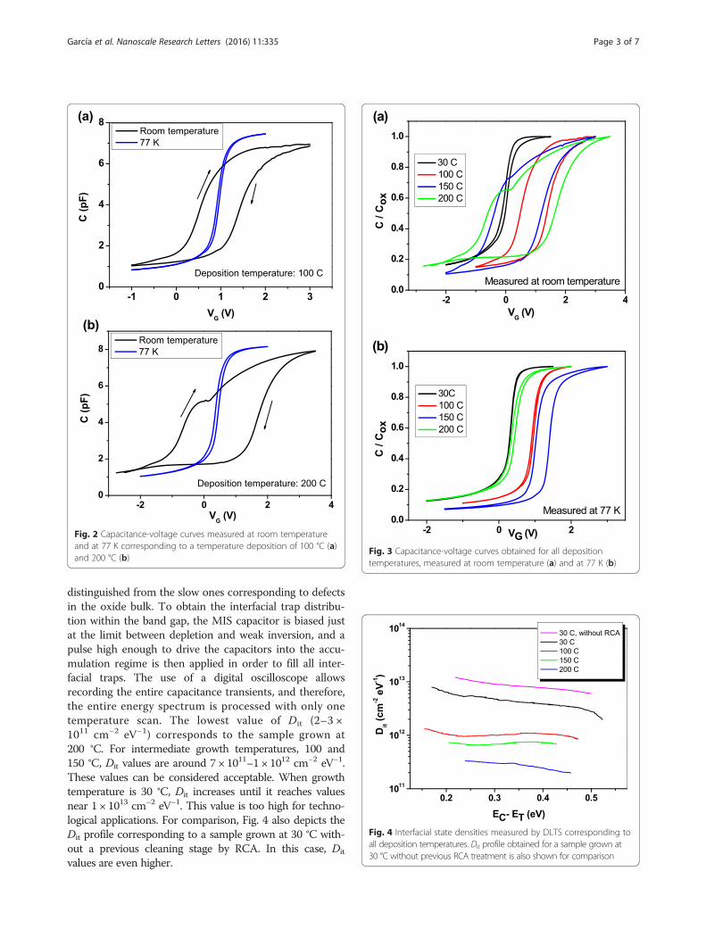
Fig. 2 Capacitance-voltage curves measured at room temperatureand at 77 K corresponding to a temperature deposition of 100 °C (a)and 200 °C (b)
Fig. 3 Capacitance-voltage curves obtained for all depositiontemperatures, measured at room temperature (a) and at 77 K (b)
Fig. 4 Interfacial state densities measured by DLTS corresponding toall deposition temperatures. Dit profile obtained for a sample grown at30 °C without previous RCA treatment is also shown for comparison
García et al. Nanoscale Research Letters (2016) 11:335 Page 3 of 7
distinguished from the slow ones corresponding to defectsin the oxide bulk. To obtain the interfacial trap distribu-tion within the band gap, the MIS capacitor is biased justat the limit between depletion and weak inversion, and apulse high enough to drive the capacitors into the accu-mulation regime is then applied in order to fill all inter-facial traps. The use of a digital oscilloscope allowsrecording the entire capacitance transients, and therefore,the entire energy spectrum is processed with only onetemperature scan. The lowest value of Dit (2–3 ×1011 cm−2 eV−1) corresponds to the sample grown at200 °C. For intermediate growth temperatures, 100 and150 °C, Dit values are around 7 × 10¹¹–1 × 1012 cm−2 eV−1.These values can be considered acceptable. When growthtemperature is 30 °C, Dit increases until it reaches valuesnear 1 × 1013 cm−2 eV−1. This value is too high for techno-logical applications. For comparison, Fig. 4 also depicts theDit profile corresponding to a sample grown at 30 °C with-out a previous cleaning stage by RCA. In this case, Dit
values are even higher.

Fig. 6 Flat-band transients measured at room temperature fromaccumulation and from inversion, corresponding to a sample grownat 100 °C
García et al. Nanoscale Research Letters (2016) 11:335 Page 4 of 7
Border trap densities obtained by means of conduct-ance transient analysis are of the same order of magni-tude for the samples grown at 100, 150, and 200 °C. Asan illustration, Fig. 5 shows the three-dimensional plotof disorder-induced gap state density (NDIGS) as a func-tion of the energy and the spatial coordinate for thesample grown at 100 °C. It can be seen that NDIGS valuesare in the range of standard MIS devices. On the otherhand, for the sample grown at 30 °C, conductance tran-sient amplitudes are below the experimental resolution,so we can conclude that its border trap density is lowerthan 1 × 1010 cm−2 eV−1. This result agrees well with thehigh value of Dit measured in this sample, because ingeneral, when border trap density (NDIGS) is high, inter-facial state density (Dit) is low [17]. So, for the samplegrown at 30 °C, fast traps are preferentially located atthe insulator/semiconductor interface, whereas for sam-ples grown at 100–200 °C, fast traps are defects locatedboth at the interface and in the insulator.Figures 6, 7, and 8 are related to flat-band transient re-
cordings. Figure 6 demonstrates for the sample grown at100 °C that there are flat-band transients at roomtemperature when the sample is previously biased in ac-cumulation or in inversion for a few seconds. In bothcases, it is possible to obtain an Arrhenius plot by re-cording transients at different measurement tempera-tures. Measurements were carried out at a voltage biasof 0 V, keeping the capacitance at its flat-band value.The flat-band voltage transients are due to trap chargingand discharging of defects inside the oxide layer. Thismechanism gives rise to variations in flat-band voltagevalue due to changes in the oxide charge density [18].As the charge trapping or detrapping inside the oxide isusually tunneling assisted, states located deeper in theoxide capture carriers after those located near the semi-conductor/oxide interface, so the VFB transients obtained
Fig. 5 Border trap three-dimensional distribution of a sample grownat 100 °C
are expected to be slower than the DLTS transients. InFig. 7, we can see that the transient amplitudes initiallyincrease with growth temperature, reach their maximumvalue at 150 °C, and then diminish while transients be-come faster. In Fig. 8a, we show the flat-band voltagetransients recorded at temperatures varying between 195and 275 K for the sample grown at 200 °C. The ampli-tude of transients is thermally enhanced, and thetemperature dependence of the transient amplitude fol-lows an Arrhenius plot (Fig. 8b). The linear fit providesan activation energy value of 88 meV. Similar values areobtained for all the samples. In the case of high-k dielec-trics, the activation energy has been found to be similarto the soft optical phonon energies [19].Figure 9 shows current-voltage curves corresponding
to the accumulation regime, measured at roomtemperature and at 77 K. The best behavior corresponds
Fig. 7 Flat-band transients from accumulation measured at roomtemperature corresponding to all deposition temperatures

Fig. 8 Flat-band transients from accumulation measured at differenttemperatures (a) and Arrhenius plot (b) of a sample grown at 200 °C
Fig. 9 Current-voltage curves measured at room temperature and77 K corresponding to all deposition temperatures
García et al. Nanoscale Research Letters (2016) 11:335 Page 5 of 7
to the 150 °C-deposited sample, with breakdown electricfield values corresponding to 2 mA/cm2 of around 0.35and 0.45 MV/cm, at room temperature and 77 K,respectively.Finally, to study in depth the “shoulder”-shaped fea-
ture showed in Fig. 2b, some additional measurementshave been carried out. When measurement temperaturediminishes, the feature also diminishes (see Fig. 10a). Infact, at temperatures lower than 270–280 K, it com-pletely disappears. Focusing on the C-V and G-Vcurves at room temperature, in the next experiment(Fig. 10b–d), a stair-shaped voltage was used insteadof a voltage ramp, with different values of the stepwidth, from 0 s (which corresponds to the voltageramp) until 100 s. The absolute value of the incrementof the voltage bias was 20 mV in all measurements.Both capacitance and conductance signals exhibit avery different behavior if voltage goes from accumula-tion to weak inversion or vice versa. In the formercase, C-V and G-V curves indicate that generation andrecombination through interface trap levels dominatethe loss. On the contrary, when voltage bias passesfrom negative to positive values, C-V curves show akink and G-V curves show two peaks instead of onlyone. One of these peaks remains nearly in the samevoltage position when measurement conditions arechanged. The second one appears at lower values ofthe voltage and clearly moves to higher values whenthe measurement time increases. Also, this peak di-minishes and nearly disappears for time values ofaround 100 s.The shape of C-V and G-V curves when voltage bias
values increase can be attributed to the dischargeprocess of slow states located far from the interface,which need high temperature or longer time to releasetheir positive charge. When charge emission takes place,flat-band voltage moves towards more positive values,and so the hysteresis width of C-V curves diminishes. Atthe same time, the shoulder-shaped feature vanishes. Asfor G-V curves, the second peak moves to the right andits height diminishes. So, when the samples are drivenfrom weak inversion to accumulation, the loss is due tothe generation and recombination through both bulkand interfacial trap levels.As indicated in Fig. 3a, these phenomena do not ap-
pear in samples grown at low temperatures, so the pres-ence of slow traps in the a-Si layer bulk seems to berelated to the growth processes carried out at tempera-tures above 150 °C.
ConclusionsInterfacial state density values for samples grown attemperatures of 100 °C and above are in the range ofstandard devices. Border trap densities and activation

Fig. 10 Capacitance and conductance vs. bias hysteresis loops measured at 500 kHz corresponding to a sample grown at 200 °C, at differenttemperatures, by using a voltage ramp (a), and at room temperature, by using a stair-shaped voltage, with different values of the step width(b–d). In all cases, the step of voltage bias was 20 mV
García et al. Nanoscale Research Letters (2016) 11:335 Page 6 of 7
energy values are in the standard values as well. Fromour experimental results, the optimal amorphous/crys-talline silicon interface is achieved for the highestgrowth temperature value. However, in samples grownat temperatures of above 150 °C, a significant presenceof slow traps in the a-Si layer is detected. In conclu-sion, to use these kinds of structures in the HIT solarcell application field, growing a-Si layers at 100–150 °Cseems to be the most adequate choice.
Abbreviationsa-Si:H, hydrogenated amorphous silicon layers; c-Si, crystalline silicon; C-V,capacitance-voltage; Dit, interface trap density; DLTS, deep-level transientspectroscopy; ECR-CVD, electron cyclotron resonance chemical vapordeposition; FTIR, Fourier transform infrared spectroscopy; G-V, conductance-voltage; HIT, heterojunction with intrinsic thin layer; i-a-Si:H, intrinsicamorphous silicon; I-V, current-voltage; MIS, metal-insulator-semiconductor;NDIGS, disorder-induced gap state density; PECVD, plasma-enhanced chemicalvapor deposition; RCA, Radio Corporation America; VFB, flat-band voltage
AcknowledgementsThe study has been supported by the Spanish TEC2014 under Grant Nos.52152-C3-3-R and TEC2013-41730-R, funded by the Ministerio de Economía yCompetitividad, and the P2013/MAE-2780 funded by the Comunidad deMadrid.
Authors’ ContributionsHC and IM conceived this study. RGH grew the samples with the help of JOand AP. HG, SD, and LB characterized the samples. HC wrote the manuscriptwith the input from all the authors. All authors read and approved the finalversion of the manuscript.
Competing InterestsThe authors declare that they have no competing interests.
Author details1Department of Electronics, University of Valladolid, Paseo Belén, 15, 47011Valladolid, Spain. 2Dpto. Física Aplicada III, Universidad Complutense deMadrid, CEI Campus Moncloa, UCM-UPM, Madrid, Spain.
Received: 26 May 2016 Accepted: 5 July 2016
References1. Meiling H, Brockhoff AM, Rath JK, Schropp REI (1998) Hydrogenated
amorphous and polycrystalline silicon TFTs by hot-wire CVD.J Non-Crystalline Solids. doi:10.1016/S0022-3093(98)00298
2. Tanaka M, Taguchi M, Matsuyama T, Sawada T, Tsuda S, Nakano S, HanafusaH, Kuwano Y (1992) Development of new a-Si/ e-Si heterojunction solarcells: ACJ-HIT (artificially constructed junction-heterojunction with intrinsicthin-layer). Jpn J Appl Phys 31:3518–22
3. Masuko K, Shigematsu M, Hashiguchi T, Fujishima D, Kai M, Yoshimura N,Yamaguchi T, Ichihashi Y, Yamanishi T, Takahama T, Taguchi M, Maruyama E,Okamoto S (2014) Achievement of more than 25 % conversion efficiencywith crystalline silicon heterojunction solar cell. IEEE J Photovoltaics.doi:10.1109/JPHOTOV.2014.2352151
4. Rech B, Kluth O, Repmann T, Roschek T, Springer J, Müller J, Finger F,Stiebig H, Wagner H (2002) New materials and deposition techniques forhighly efficient silicon thin film solar cells. Sol Energy Mater Sol Cells74:439–42
5. Santos JD, Cárabe J, Gandía JJ (2015) Silicon thin-film solar cells at highgrowth rate under constant power-to-flow ratio plasma conditions. ThinSolid Films. doi:10.1016/j.tsf.2015.11.011
6. Flewit AJ, Milne WI (2005) Low-temperature deposition of hydrogenatedamorphous silicon in an electron cyclotron resonance reactor for flexibledisplays. Proceed of the IEEE. doi:10.1109/JPROC.2005.851533
7. Redondo E, Mártil I, González-Díaz G, Castán H, Dueñas S (2001) Influence ofelectron cyclotron resonance nitrogen plasma exposure on the electricalcharacteristics of SiNx:H/InP structures. J Vac Sci Technol B.doi:10.1116/1.1339010
8. García-Hernansanz R, García-Hemme E, Montero D, Olea J, San Andrés E, DelPrado A, Ferrer FJ, Mártil I, González-Díaz G (2016) Limitations of high

García et al. Nanoscale Research Letters (2016) 11:335 Page 7 of 7
pressure sputtering for amorphous silicon deposition. Mater Res Express.doi:10.1088/2053-1591/3/3/036401
9. García-Hernansanz R, García-Hemme E, Montero D, Del Prado A, Mártil I,González-Díaz G, Olea J (2015) Amorphous/crystalline silicon interfacecharacterization by capacitance and conductance measurements. 10thSpanish Conference on Electron Devices Proceedings (IEEE ConferencePublication). INSPEC Accession Number: 15060343. doi:10.1109/CDE.2015.7087502
10. Schulze TF, Beushausen HN, Leendertz C, Dobrich A, Rech B, Korte L (2010)Interplay of amorphous silicon disorder and hydrogen content withinterface defects in amorphous/crystalline silicon heterojunctions. Appl PhysLett. doi:10.1063/1.3455900
11. Kern W, Puotinen D (1970) Cleaning solutions based on hydrogen peroxidefor use in silicon semiconductor technology. RCA Rev 31:187–206
12. Mahan AH, Gedvilas LM, Webb JD (2000) Si-H bonding in low hydrogencontent amorphous silicon films as probed by infrared spectroscopy and x-ray diffraction. J Appl Phys. doi:10.1063/1.372073
13. Girginoudi D, Tsiarapas C, Georgoulas N (2011) Properties of a-Si:H filmsdeposited by RF magnetron sputtering at 95 °C. Appl Surf Sci. doi:10.1016/j.apsusc.2010.11.115
14. Masson P, Autran JL, Houssa M, Garros X, Leroux C (2002) Frequencycharacterization and modeling of interface traps in HfSixOy/HfO2 gatedielectric stack from a capacitance point-of-view. Appl Phys Lett 81:3392–4
15. Stesmans A, Afanas’ev VV (2003) Si dangling-bond-type defects at theinterface of (100)Si with ultrathin HfO2. Appl Phys Lett 82:4074–6
16. Dueñas S, Castán H, Barbolla J, Kukli K, Ritala M, Leskelä M (2003)Conductance transient, capacitance–voltage and deep-level transientspectroscopy characterization of atomic layer deposited hafnium andzirconium oxide thin films. Solid State Electron 47(2003):1623–9
17. García H, Dueñas S, Castán H, Bailón L, Kukli K, Aarik J, Ritala M, Leskelä M(2008) Identification of spatial localization and energetic position ofelectrically active defects in amorphous high-k dielectrics for advanceddevices. J Non-Crystalline Solids 354:393–8
18. Dueñas S, Castán H, García H, Gómez A, Bailón L, Kuli K, Aarik J, Ritala M,Leskelä M (2008) Comparative study of flatband voltage transients on high-k dielectric-based metal–insulator–semiconductor capacitors. J ElectrochemSoc. doi:10.1149/1.2975828
19. Dueñas S, Castán H, García H, Bailón L, Kukli K, Hatanpää T, Ritala, Leskelä M(2007) Experimental observations of temperature-dependent flat bandvoltage transients on high-k dielectrics. Microelectron Reliab. doi:10.1016/j.microrel.2007.01.080
Submit your manuscript to a journal and benefi t from:
7 Convenient online submission
7 Rigorous peer review
7 Immediate publication on acceptance
7 Open access: articles freely available online
7 High visibility within the fi eld
7 Retaining the copyright to your article
Submit your next manuscript at 7 springeropen.com