Embed Size (px)
Citation preview

ELEC4705 – Fall 2009Tom Smy
LECTURE 13The Diode
1


ContentsELEC4705 – Fall 2009 1
Lecture 13. The Diode 113.1. Schottky Barriers (Metal-Semiconductor Junctions) 413.1.1. Material Band Structures 413.1.2. Semiconductor Band Structure (conduction and valance
band, n-type) 513.1.3. Metal-Semiconductor Junction - the thought
experiment 613.1.4. Reverse bias (V < 0) 813.1.5. Forward Bias 813.1.6. Applications 1013.2. PN Junction 1213.2.1. Values for φ and W 1813.2.2. Forward Bias 1913.2.3. Reverse Bias 2113.2.4. I-V Characteristics for Diode 23
3

4 TOM SMY, DEVICES MATERIALS AND PROPERTIES
The first device we will look at is the diode. The diode is a non-linear device (I is not proportional to V) formed by creating a devicefrom a metal and a semi-conductor (Schottky diode) or two types ofsemi-conductor one n and the other p type (pn diode).
13.1. Schottky Barriers (Metal-Semiconductor Junc-tions)
Schottky diodes (see figure 1) are the oldest semiconductor devicesused as rectifiers in ”crystal” radios. Later they were replaced by pn-junctions. A Schottky diode is a special type of diode with a very lowforward-voltage drop which are based on a metal-semiconductor junc-tion. When current flows through a diode there is a small voltage dropacross the diode terminals. A normal diode has between 0.7− 1.7 voltdrops, while a Schottky diode voltage drop is between approximately0.15− 0.45 volts.
They still have a number of uses and the physical effects on whichtheir operation is based are present in many situations.
The lower voltage drop translates can translate into higher systemefficiency.
Figure 1. Symbol of a Schottky Diode
13.1.1. Material Band Structures
At surface of any solid there is an energy barrier holding in the electrons(work function), i.e. the work function is the minimum energy neededto remove an electron from a solid to a point immediately outside thesolid surface (or energy needed to move an electron from the Fermienergy level into vacuum).

TOM SMY, DEVICES MATERIALS AND PROPERTIES 5
Figure 2. Metal Band Structure
13.1.1.1. Metal Band Structure (half filled band). See figure 2.
• φm is the work function or (ionization energy) which is theenergy to remove the electron from the Fermi level to vacuumlevel.
• The work function φm is strongly dependent on surface prepa-ration and is not a precisely defined quantity (varies dependingon surface).
13.1.2. Semiconductor Band Structure (conduction and valanceband, n-type)
See figure 3
Figure 3. Semiconductor Band Structure

6 TOM SMY, DEVICES MATERIALS AND PROPERTIES
• Work function φs depends on doping, however it is often moreuseful to deal with the electron affinity χ (energy to removeelectron from conduction band) χs ≈ 4.1eV for Si.
13.1.3. Metal-Semiconductor Junction - the thought experi-ment
As for the pn diode we undertake a thought experiment where we bringthe two materials into contact and equilibrate the Fermi energies.
Figure 4 shows the band structures of metal and semiconductorwhen the materials don’t touch and (φm > φs).
Figure 4. Metal-Semiconductor Band Structure Before Touching

TOM SMY, DEVICES MATERIALS AND PROPERTIES 7
After the metal and semiconductor have been brought into contact,electrons start to flow from the semiconductor down into the metal untilthe Fermi energies of both solids are equal (equilibrium condition), seefigure 5 for the band structure.
Figure 5. Metal-Semiconductor Band Structure After Touching
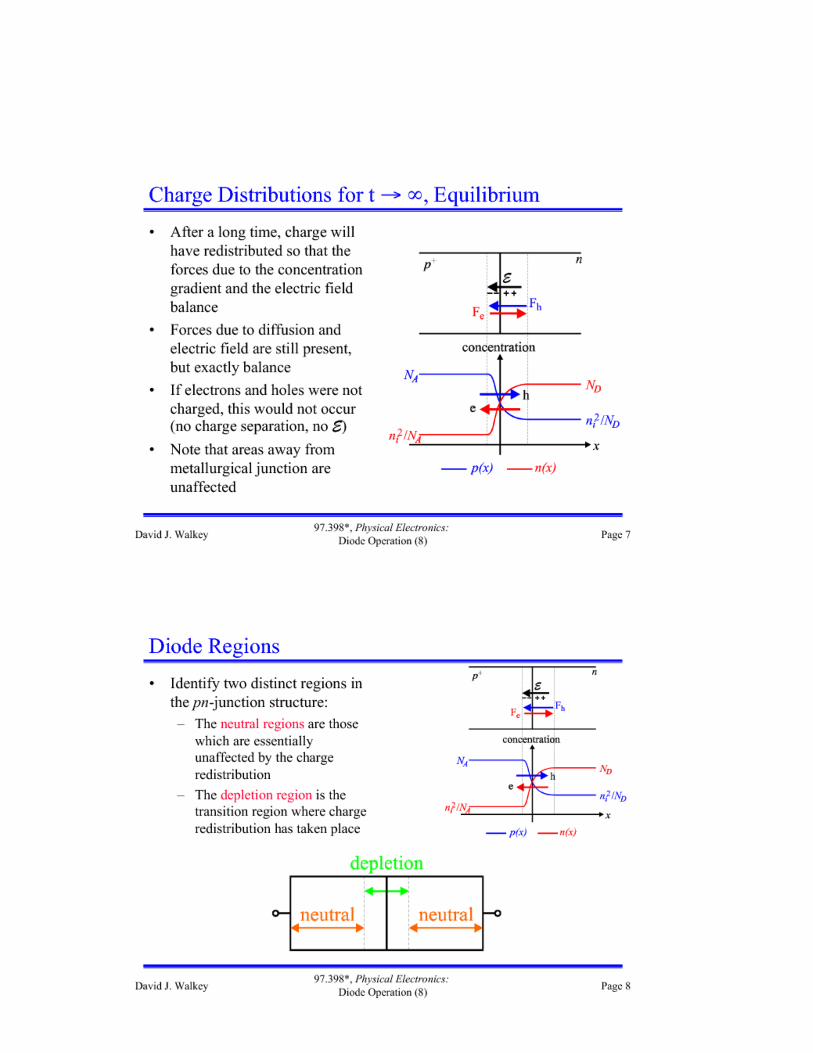
• In the semiconductor, a depletion region of width W is formed(uncompensated donors).
W =
√2εiV0
qND
(13.1)
• In the metal an electron current forms a negative surface chargelayer.
• These in turn produce an electric field is created.• An electric potential is established and a bending of the bands
occurs in the semiconductor.
V0 =φm − φs
q=
KT
qln(
Nc
ND
) (13.2)
• V0 and W both depend on doping concentration (ND) andtemperature.
We have two currents flowing (majority carriers n in this case) oneJsm from the semiconductor to the metal over the barrier φm− φs andthe other Jms from the metal to the semiconductor over the barrier χ.The equilibrium is reached when the two equal and opposite electron
flow over the barrier and J = 0 at V = 0.

8 TOM SMY, DEVICES MATERIALS AND PROPERTIES
13.1.4. Reverse bias (V < 0)
If the metal is connected to the negative terminal of a battery, themetal is charged even more negatively than without bias, see figure 17.
Figure 6. Metal-Semiconductor Band Structure in Reverse Bias
We see similar effects as with the pn diode.
• The electrons in the semiconductor are repelled even more.– Depletion region becomes wider.– Potential barrier is increased.
• The electron flows are unbalanced since the Jsm → 0.• A current flows as a result of a few electrons in the metal
acquiring enough thermal energy to overcome barrier. This isa small current as barrier φm − χ has not changed, and Jms isas before.
• At high reverse bias, electrons can tunnel through barrier “fieldemission” and cause a charge current to flow.
13.1.5. Forward Bias
Now consider the case when the polarity of the battery is reversed, i.e.metal is connected to the positive terminal of the battery, see figure 15

TOM SMY, DEVICES MATERIALS AND PROPERTIES 9
for the band structure.
Figure 7. Metal-Semiconductor Band Structure in Forward Bias
• The electrons spill from semiconductor into metal.– Depletion region becomes narrower.– Potential barrier is reduced.
• We get a large current exponentially related to V flowing inthe device.
• To compute the electron flow from semiconductor to metal weuse thermionic emission theory. The current that flows fromthe metal into the semiconductor is given by
Jms =q4πm∗K2T 2
h3e−q(φm−χ)/KT . (13.3)
Where C = q4πm∗K2/h3 is defined as Richardson’s Constant.So we have the current as
Jms = CT 2 e−q(φm−χ)/KT . (13.4)
• The current flowing from the semiconductor into the metal is
Jsm = CT 2 e−q(φm−φs−V )/KT . (13.5)
• The net current is given by
Jnet = Js(eqV/KT − 1) , Js = CT 2 e−q(φm−φs)/KT (13.6)

10 TOM SMY, DEVICES MATERIALS AND PROPERTIES
As typically there is very little minority carrier injection fromsemiconductor into metal; Schottky diodes are said to be majority
carrier devices.
13.1.6. Applications
13.1.6.1. Ohmic Contacts to Semiconductors. In Integrated Circuitsthe external connections are always metallic. A metal-semiconductorjunction, which conducts current in only one direction, may be prob-lematic. Need to make a low resistance contact with linear V-I charac-teristics, see figure 11(b).
Figure 8. Ohmic Contacts to Semiconductors
In case of φm < φs, the electrons flow from the metal into the semicon-ductor, see figure 9 for the band structure before touching.

TOM SMY, DEVICES MATERIALS AND PROPERTIES 11
Figure 9. Metal-Semiconductors Band Structure in case of φm <φs before touching
After connecting the two materials we will have:
• In metal, electron current forms a positive surface charge layer.• An electric field is created (in the opposite direction as before).• An electric potential and thus a bending of the bands occurs,
see figure 10.
Figure 10. Metal-Semiconductors Band Structure in case of φm <φs after touching
• The bands of the semiconductor bend downward and no barrierexists for the flow of electrons in either direction.
• The current increases linearly with increasing voltage and issymmetric about the origin, see figures 11(a) and 11(b).

12 TOM SMY, DEVICES MATERIALS AND PROPERTIES
(a) Schottky barrier (b) what we need for an ohmic contact
Figure 11. I-V characteristics for a Schottky junction and anOhmic contact
13.1.6.2. Notes on the applications.
• Since only majority carriers are involved, no mutual annihila-tion (recombination) of electrons and holes can occur. Thisresults in faster devices.
• The metal base provides better heat removal and is helpful inhigh power devices.
• Used for detection of long wavelength IR (low energy photons).This is useful in temperature sensors.
13.2. PN Junction
The device operation can be best explained by its band structure andcarrier concentrations. We can understand this using a thought exper-iment where we bring together two pieces of material one n and theother p as shown in figure 12.
Due to diffusion we have two effects:
• Electrons pour out of n-type material, leaving behind uncom-pensated donors (+ ions)
• Holes pour out of p-type material, leaving behind uncompen-sated acceptors (- ions)
These electrons and holes then recombine, producing a region aroundthe interface depleted of free carriers, leaving only fixed charges (ionizeddonors and acceptors). However the diffusion process can not continueindefinitely as this space charge creates an electric field that opposes the

TOM SMY, DEVICES MATERIALS AND PROPERTIES 13
Figure 12. PN Junction
diffusion of majority carriers (electrons in n type and holes in p type),though such diffusion is not prevented altogether as shown in figure 13.The electric field will sweep minority carriers (holes in n − type and
Figure 13. Built in electrin field
electrons in p− type) across the junction so that there is a drift currentof electrons from the p− to the n− type side and of holes from the n−to the p− type side which is in the opposite direction to the diffusioncurrent. The junction field builds up until these two current flows areequal and equilibrium is achieved (no net current flow).
It is a basic result of thermodynamics that in equilibrium the Fermienergy must be the same throughout the system.
The induced electric field establishes a contact potential φ between thetwo regions and the energy bands of the p − type side are displacedrelative to those of the n− type side. This produces the Energy BandDiagram for a p-n Junction as shown in figure 14.

14 TOM SMY, DEVICES MATERIALS AND PROPERTIES
Figure 14. Band structure of a diode
Now lets look at the carrier concentrations in the device during thethought experiment.

TOM SMY, DEVICES MATERIALS AND PROPERTIES 15

16 TOM SMY, DEVICES MATERIALS AND PROPERTIES
TOM SMY, DEVICES MATERIALS AND PROPERTIES 17

18 TOM SMY, DEVICES MATERIALS AND PROPERTIES
13.2.1. Values for φ and W
The electrostatics and the fact that at equilibrium the current throughthis device must be zero can be use to solve for the built in potentialand the width of the depletion region.
For a uniform junction Nd = Const. and NA = Const. the built inpotential (φ) and the width of the depletion region (W ) are as follows.
φ =KBT
qln(
NAND
n2i
) (13.7)
W =
√2εSiφ
q
√NA + ND
NAND
(13.8)
Notes:
• εSi is the electric permitivity of Silicon.• The built in potential (φ) depends on doping and temperature.
13.2.1.1. A special case. In practice, we often encounter one-sided (oneside much more heavily doped than the other) abrupt junctions andthen for the depletion width (equation 13.8)we will have
W =
√2εSiφ
qNB
(13.9)
NB = NA if ND � NA
NB = ND if NA � ND
NOTE:Even for zero bias, there are electron and hole flows across the junctionwhich exactly balance, i.e.
Je(drift) + Je(diffusion) = 0
Jh(drift) + Jh(diffusion) = 0

TOM SMY, DEVICES MATERIALS AND PROPERTIES 19
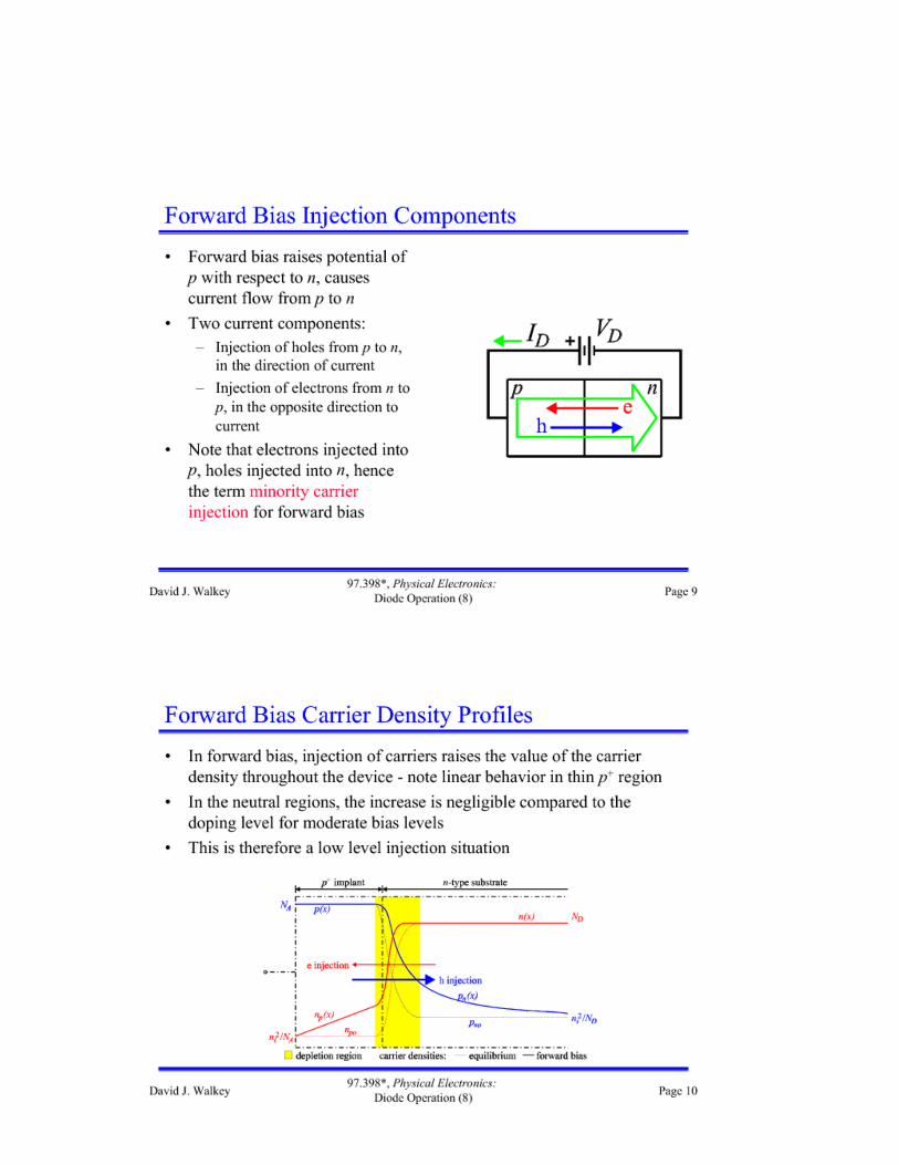
13.2.2. Forward Bias
Consider now the case when the n− side is connected to the negativeterminal of the dc source, then the depletion region narrows,as shownin figure 15. This has the effect of lowering the height of the potential
Figure 15. Forward Bias
barrier to (φ−V ). Consequently, majority carriers are able to surmountthe potential barrier much more easily than in the equilibrium case sothat the diffusion current becomes much larger than the drift current.See figure 16 for the band structure in forward bias.
Figure 16. Forward Bias
20 TOM SMY, DEVICES MATERIALS AND PROPERTIES
TOM SMY, DEVICES MATERIALS AND PROPERTIES 21
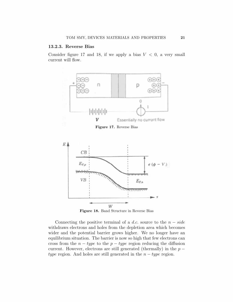
13.2.3. Reverse Bias
Consider figure 17 and 18, if we apply a bias V < 0, a very smallcurrent will flow.
Figure 17. Reverse Bias
Figure 18. Band Structure in Reverse Bias
Connecting the positive terminal of a d.c. source to the n − sidewithdraws electrons and holes from the depletion area which becomeswider and the potential barrier grows higher. We no longer have anequilibrium situation. The barrier is now so high that few electrons cancross from the n − type to the p − type region reducing the diffusioncurrent. However, electrons are still generated (thermally) in the p −type region. And holes are still generated in the n− type region.

22 TOM SMY, DEVICES MATERIALS AND PROPERTIES

TOM SMY, DEVICES MATERIALS AND PROPERTIES 23
13.2.4. I-V Characteristics for Diode
We can solve for the current flow through the device by using minoritycarrier diffusion. For the diffusion current we have Jforward ∝ eqVb/KBT .
Excitation of electrons over a barrier is exponen-tial! And proportional to eqVb/KBT
J = J0(eqV/KBT − 1) (13.10)

24 TOM SMY, DEVICES MATERIALS AND PROPERTIES

TOM SMY, DEVICES MATERIALS AND PROPERTIES 25
Summary of ideal diode equation:
• As the ideal diode equation indicates the current is very strongtemperature and bias.
• For forward bias (positive V ) the net current increases expo-nentially with voltage.
• For reverse bias (negative V ) the current is essentially constantand equal to J0.
• The reverse bias generation current is small compared with theforward bias current.
• A typical I-V curve for a diode is shown in figure 19. Thereverse saturation current i0is equal to J0 multiplied by thejunction cross-sectional area (A).
Figure 19. Current- Voltage Characteristic of a pn junction diode
There is also the generation of hole/electron pairs in depletion re-gion and these cause small additional current. Therefore we have asmall leakage current (equation 13.11)as these electrons and holes areswept across the depletion region (drift current).
J0 = q(Dh
Lh
pn +De
Le
np) (13.11)
• In order to keep J0 small, the minority carriers (pn and np) haveto be kept at low levels. This can be accomplished by selectingsemiconductors having a large energy gap and by high doping.
• The drift current is relatively insensitive to the height of thepotential barrier since all of the minority carriers generatedmay diffuse to the depletion region and be swept across it.