Embed Size (px)
Citation preview

Westinghouse I.L. 43-846.1A
INSTALLATION • OPERATION • MAINTENANCE
INSTRUCTIONS WATT TRANSDUCER TYPE VP4-846
VAR TRANSDUCER TYPE VV4-846
The type VP4-846 Watt Transducer and VV4-846 Var Transducer are solid state devices which produce a de output directly proportional to the ac power (real or reactive) appearing at its input. This proportionality is maintained with reversal of power flow, since the de output changes polarity accordingly. Styles are available with either ± 10% or 0-110% adjustment of the nominal 0 to ± 1 mAde output current which is independent of load from 0 to 10,000 ohms.
THEORY OF OPERATION
This new solid state watt transducer employs the time division multiplication principle. This method for measuring watts requires the generation of a train of pulses whose height is proportional to the amplitude of the current and whose length is proportional to the amplitude of the potential. If the number of pulses is large compared to the frequency of the measured waveform, the area of each pulse (i.e. the time integral of current flowing during the pulse) will be equal to the instantaneous power flowing in the measured circuit over the duration of the pulse. Integrating these pulses with a low pass filter removes the ac products of the multiplication leaving a de signal which is proportional to the power being measured.
This relatively high level de signal is applied to an operational amplifier, which provides the "constant-current" type of output. The high level input current eliminates the need for a zero adjust-
ment of the operational amplifier, in contrast to Hall generator types which require zero adjustment as a result of their inherent low voltage output to a high gain operational amplifier. Critical electro-mechanical assemblies have also been eliminated as this is an all solid state design using the latest I.C. technology including complimentary MOS digital I.C.'s.
Var (reactive power) transducers are similar to the watt transducer except the potential circuits are shifted 90° in phase by means of a R-C network, so that the multiplier responds to EI sin 9, compared to EI cos g for real power.
3 Phase 3 Wire units employ two multipliers and perform with rated accuracy for any current or voltage unbalance. The 3 Phase 4 Wire units employ 2 multipliers also but use 3 current signals and 2 potential signals (known as 21/2 element connection) to derive the 4 wire power. These units perform at rated accuracy for any current unbalance, but the system voltages should be balanced for best accuracy. Only two potential transformers need be provided on the system with this circuit.
CALIBRATION PROCEDURE
(WHEN RE-CALIBRATION IS DESIRED)
These transducers may be calibrated on single phase by connecting the potential circuits in parallel and the current circuits in series as shown in Fig. 4 for 3 phase, 3 wire, and as shown in Fig.
A II possible contingencies which may arise during installation, operation, or maintenance, and all details and variations of this equipment do not purport to be covered by these instructions. If further information i.� desired by purchaser regarding his particular installation, operation or maintenance of his equipment. the local Westinghouse Electric Corporation representative should be contacted.
Supersedes I.L. 43-846.1, dated June 1975 0 Denotes change from superseded Issue.
EFFECTIVE NOVEMBER 1976 www . El
ectric
alPar
tMan
uals
. com

0
5 for 3 phase, 4 wire. (Note that the current circuit connected to terminals #13 and #14 of the 4 wire unit must be connected with reverse polarity in comparison to the other current circuits to achieve proper single phase operation. This is characteristic of the 21/z element principle. Failure to do this will result in zero output irrespective of input). The single phase test watts required for calibration are calculated as follows:
3 phase, 3 wire
l 0 test watts (or vars)
(2 El.) ( Desired self-contained*) 3 0 input watts [or vars]
_for rated output 2
0 3 phase, 4 wire (2'1z El.)
l 0 test watts (or vars)
6Desired self-contained*) 30 input watts [or vars]
= or rated output 4
NOTE: *For power systems which use current and/ or potential transformers the desired self-contained 3 0 input watts for the transducer are the system watts for rated output divided by the transformer ratios.
The power supply terminals # l and 2 should be energized for at least 15 minutes before calibration to pre-condition the transducer.
The calibration adjustment for the total output, both watt and var transducers, is available through a hole in the top panel adjacent to terminal #5, and is labeled "CAL". This control allows the nominal l rnA de output for rated input to be scaled ± 10% or 0 to 110% depending on the transducer style. All other adjustments are factory-set adjustments, and should not be disturbed unless a complete re-calibration can be performed.
The "CAL" adjustment does not change the voltage or current input ratings of the transducer, but only sets the output. The large over-range capability does allow wide latitude in the permissible input level, however. On the watt transducer
2
individual element output adjustment is available by adjusting the trimmers through holes near terminals #6 and #10. These should not be adjusted unless a complete re-calibration procedure can be done, since the elements are balanced by these trimmers.
Var transducers can be calibrated in a similar single phase fashion except that a V AR standard must be used instead of a watt standard. A wattmeter standard provided with a 90° phase shifting network and having a l: l transfer ratio can be used. The calibration adjustment for the total output is the same as the watt transducer, but individual element balance adjustment for the V AR transducer is through holes in the base. In addition, each V AR element has an adjustment for phase shift through the base. The trimmers available through holes in the base should not be adjusted unless a complete recalibration procedure can be done.
ADJUSTMENT SCREW DRIVER SIZE A small diameter instrument-type screw driver
with a 0.1 in. wide X 0.02 in. thick bit is recommended.
ZERO ADJUSTMENT
There is no zero adjustment ever required on ± 10% adjustment units because of the nature of their design. DC output current comes from a modulated current signal which has been obtained from an internal current transformer. No amplifiers have been employed in this circuit. This current signal is then run thru a "current pump" to permit supplying load resistances up to l OK.Q . (The current pump would not be required if the load resistance range had been limited to a few hundred ohms).
The "current pump" operates as a l: 1 current amplifier. The I.C. voltage offset and its temperature coefficient do not appear in the output with this circuit. Because the input is already 1 rnA, the bias current of the I.C. is insignificant, hence no zero adjustment is required.
The 0 to ll 0% adjustment units, however, do have an internal zero adjustment. Normally this is
www . El
ectric
alPar
tMan
uals
. com
adjusted once at the factory and does not require any further attention. This is used because the large range of adjustment requires the use of another I.C. Repairs to the unit, particularly replacement of the type 747 integrated circuits, may require touching up this adjustment. It is also advisable when doing a complete recalibration to check and touch up the adjustment if required.
To reach the zero adjustment trimmer, remove the self threading binding head screws located on the ends of the case, and remove the case. The adjustment is a single turn pot located on the power supply printed circuit board approximately below terminal # l l on the top panel. Apply 120 volts ac to the power supply terminals #1 and 2 and both element potential circuits on terminals #3 and 4 and #7 and 8. Allow 15 minutes warm up. Then adjust the trimmer to get zero output (less than ±0.2 micro amps or ±2 millivolts across a lOKQ load).
COMPLETE RECALIBRATION ·WATTS
Connect the transducer as shown in Fig. 4 for a 3 phase, 3 wire unit and as shown in Fig. 5 for a 3 phase, 4 wire unit. Set the calibration adjustment adjacent to terminal #5 fully clockwise. Open the potential circuit to terminals #7 and 8 and apply rated single phase test watts to the transducer. Adjust the trimmer through the hole adjacent to terminal #6 to obtain 56% of rated output. Now apply reversed potential to terminals #7 and 8 and adjust the trimmer through the hole adjacent to terminal #12 to get zero output within ±0.125% of rated output. (This balances elements by opposing them and adjusting for zero output). Restore terminals #7 and 8 to the correct polarity as given by the appropriate test connection diagram. Apply precise single phase test watts to the transudcer and adjust the calibration trimmer through the hole adjacent to terminal #5 for the required output ±0.25%.
COMPLETE RECALIBRATION • VARS
Connect the transducer as shown in Fig. 4 for a 3 phase, 3 wire unit, and as shown in Fig. 5 for a 3 phase, 4 wire unit. Set the calibration adjustment
I.L. 43-846.1 A
adjacent to terminal #5 on the top panel fully clockwise. Open the potential circuit to terminals #7 and 8 and apply unity power factor watts from a non-inductive load bank to the transducer. Set the watts to be approximately equal to the rated single phase test vars of the transducer. Turn the trimmer through hole G 1 (See Fig. 6), in the base of transducer fully clockwise. Adjust the pot through hole P l in the base of the transducer to get zero output within ±0.125% of rated output. This sets the 90° phase shift network for element #1. Restore potential to terminals #7 and 8 and open the potential circuit to terminals #3 and 4. Turn the trimmer through hole G2 in the base of the transducer fully clockwise. Adjust the trimmer through hole P2 to get zero output within ±0.125% of rated ouput. This sets the 90° phase shift network for element #2.
Restore potential to terminals #3 and 4 and open the potential circuit to terminals #7 and 8. Apply rated single phase test VAR's to the transducer. Adjust the trimmer through hole G 1 in the base of the transducer to get 56% of rated output. Apply reversed potential to terminals #7 and 8 and adjust the trimmer through hole G2 to get zero output within ±0.125% of rated output. (This balances elements, by opposing them and adjusting for zero output). Restore terminals #7 and 8 to the correct polarity as given by the appropriate test connection diagram. Apply precise single phase test V AR's to the transducer and adjust the calibration trimmer through the hole adjacent to terminal #5 on the top panel for the required output ±0.25%.
CAUTION: Attempts to get significantly more than the nominal ± l rnA rated output by complete recalibration may result in the loss of voltage overrange capability or even voltage non-linearity if carried to the extreme.
CAUTION: These transducers are equipped with CMOS integrated circuits that are susceptible to damage by static electric charges applied to their leads when they are not in their sockets. Therefore, if repairs are ever required, the following precautions are recommended:
3 www . El
ectric
alPar
tMan
uals
. com

I. Never install or remove any integrated circuit from a transducer which is energized.
2. The transducer and the technician making the repairs should be grounded.
3. Soldering irons used on the printed circuit boards should be grounded.
4. Loose CMOS integrated circuits should be stored only in conductive carriers, stuck into conductive foam or wrapped in aluminum foil.
CONSTRUCTION
All components are on two printed circuit boards mounted back to back perpendicular to the top panel. One board contains the switching function components the other board the power supply, triangle wave generator and output buffer a1J1plifier. All integrated circuits are mounted in sockets to facilitate repairs. The complete assembly is mounted in a 3" wide rectangular case suitable for base mounting, with top connected terminals. The case may be removed be removing 2 screws from the ends of the case. All solid state devices have a storage temperature range of at least -40°C to+ 100°C. The external connections and output calibration control are available from the top panel, as are the element trimming adjustments of the watt transducers. The V AR transducers are similar except the element trimming and phase shift adjustments are located through holes in the base. The element trimming and phase shift adjustments are factory set and are not affected by the top panel calibration adjustment. The transducers are available with ± 10% and 0-110% output calibration adjustment.
Transient protection, over current protection and protection against electromagnetic interference are built in. Low temperature coefficient resistors and zeners are used to obtain low temperature influence without resorting to resistorthermistor temperature compensation schemes. Good temperature performance is designed in, not compensated in as with Hall generator transducers.
The external power connections for the
4
transducer's power supply are brought out to a separate set of terminals which are connected at the factory by external jumpers to one of the watt potential circuits. If the potential circuits are to be operated at voltages below the minimum required power supply voltage of 85 volts, or if the transducer is to be used in a current totalizing scheme where the potential circuit is turned off when the other totalized transducers are still operating, then the jumpers should be removed and separate excitation at rated voltage should be supplied to terminals #I and 2.
APPLICATION
The current-output transducer with capability of supplying load resistances up to 10,000 ohms without changing calibration is well suited for applications where the load resistance is a high resistance device, or where the load resistance varies and constant current is desired.
TOTALIZING
VOLTAGE SUMMING Any number of transducers may be used, and
the transducers themselves do not have to be calibrated to the required scale. Instead the voltage drop generated across a resistor can be adjusted by varying the resistance to give the correct scale from a transducer with standard calibration. All the individual dropping resistors are then connected together in series to provide a totalized voltage which must be measured by a high impedance device. To limit the error caused by the readout device loading the measured circuit, the measurement device should have an input impedance of at least 1000 times the sum of the resistances of the dropping resistors.
Simultaneous local indication is also possible as long as the maximum voltage output required of any transducer by the local indicator, the dropping resistor and the wiring does not exceed 11 volts.
Because of the ease of scaling the individual sources and the absence of an error in the output if one of the transducers is not energized, this is the preferred way to totalize these transducers.
www . El
ectric
alPar
tMan
uals
. com
CURRENT SUMMING Any number of transducers may be totalized
by calibrating each unit as required for correct scaling and connecting all the outputs in parallel. One restriction is that all power supplies must be energized even if only one transducer is producing an output. This is necessary because the output impedance of a transducer is much smaller when the transducer is not energized and can load the external circuitry. Another restriction occurs because the maximum output voltage that the transducers can develop into an external load is limited. The totalized current of all units at maximum output cannot develop greater than 11 volts across the output of any transducer.
This connection can be useful in spite of its limitations if both local and remote indication on de instruments are desired, or if the monitoring of all the individual outputs as well as the total is desired. Otherwise the voltage summing technique is best.
REPAIRS Repair work is best done at the factory, or at
any authorized instrument repair facility (see Service Directory 43-000). However, for those customers who wish to do their own repairs and are competent in working with small signal solid state devices Figures 8 to 16 includes schematic diagrams, board layouts, voltages and waveforms that should assist in trouble shooting and making repairs.
BASIC PRINCIPLES OF TROUBLESHOOTING
Connect in single phase test circuits as shown.
If at proper input the output is as follows:
Half Output - would indicate one element may be defective. Disconnecting one current circuit at a time will enable determining which element is operating and which is not. If one element is operaing then the power supply and triangle wave generator must be operating.
I.L. 43-846.1A
Troubleshoot the switching circuit of the inoperative element.
NO OUTPUT If the power supply, or the triangle wave
generator, or the output stage is defective no output will be obtained. Troubleshoot these areas, checking for the voltages and wave forms at the various points as shown. COMPONENT CHECKING
Components may be checked for opens or shorts, but it should be observed the nature of the circuit connected to these components will affect the reading of any ohmmeter used. INTEGRATED CIRCUIT CHECKING:
All integrated circuits are mounted in sockets for easy replacement. Unless an integrated circuit tester is available, the I.C. can only be checked by inserting in a working transducer, or by replacing with an I.C. known to be good. When inserting I.C. be sure alignment and orientation is correct. Observe the precautions about handling I.C.'s. TRANSISTOR CHECKING
Transistors may be ckecked without power on by using an ohmmeter on the 100X range. A good transistor will give the following readings with the ohmmeter polarity as shown Fig. 8. (Check the ohm meter polarity against a voltmeter, do not assume polarity from terminal color marking.)
Any circuit elements shunting the transistor terminals will change the actual readings, but usually resistor values are such that conducting versus non-conducting readings can be determined. The transistors are mounted approximately 3 j 16 inch off the board, so an in-circuit transistor tester can be used too.
Diodes can be checked with an ohmmeter also. An ohmmeter across the diode will indicate as shown in Fig. 7.
Zener diodes are more difficult to check because the non-conducting direction is voltage sensitive,
5 www . El
ectric
alPar
tMan
uals
. com
but they can be checked for shorts or opens the same as regular diodes. For this check the diode zener voltage must be greater than the ohmmeter voltage. Zener diodes will appear to be non conducting in both directions if the voltage applied
is below the zener voltage.
Transformers can be checked for continuity or for actual voltage output in the energized transducer.
6
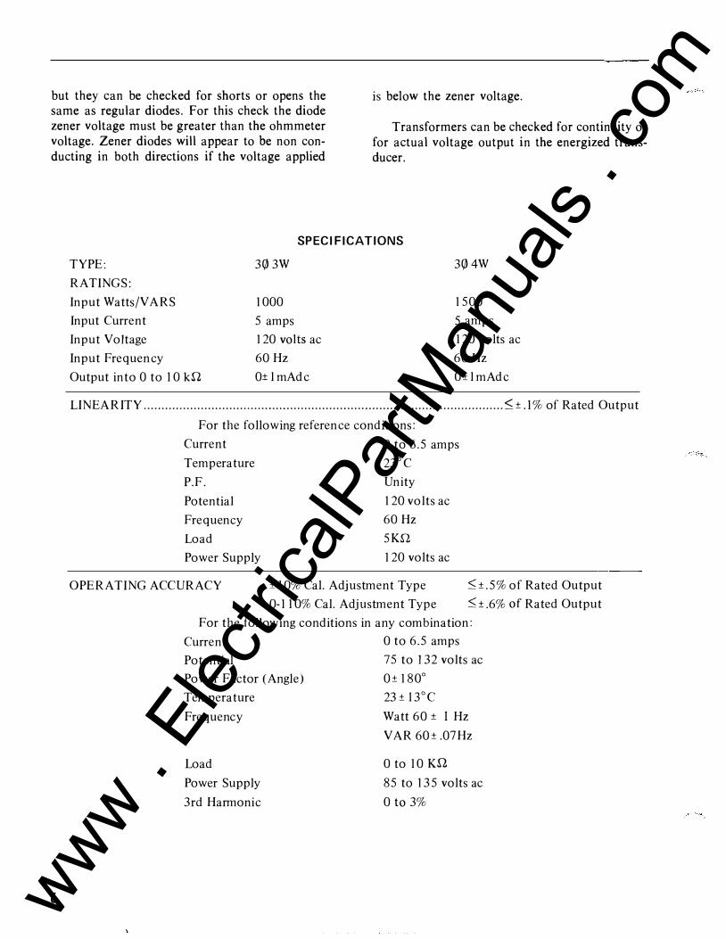
TYPE:
RATINGS:
Input Watts/VARS
Input Current
Input Voltage
3()3W
1000
5 amps
SPECIFICATIONS
3()4W
1500
5 amps
Input Frequency
Output into 0 to I 0 k.rl
120 volts ac
60 Hz
0± l mAdc
120 volts ac
60 Hz
O±l mAdc
LINEARITY . . . . . . . . . . . . . . . . . . . . . . . . . . . . . . . . . . . . . . . . . . . . . . . . . . . . . . . . . . . . . . . . . . . . . . . . . . . . . . . . . . . . . . . . . . . . . . . . . . . . . ::;± .I% of Rated Output
For the following reference conditions:
Current 0 to 6.5 amps
Temperature 23°C
P.F.
Potential
Frequency
Load
Power Supply
OPERATING ACCURACY
Unity
120 volts ac
60 Hz
5K.rl
120 volts ac
±I 0% Cal. Adjustment Type
0-110% Cal. Adjustment Type
::; ± .5% of Rated Output
::;± .6% of Rated Output
For the following conditions in any combination:
Current 0 to 6.5 amps
Potential 75 to 132 volts ac
Power Factor (Angle) 0± 180°
Temperature
Frequency
Load
Power Supply
3rd Harmonic
23 ± l 3°C
Watt 60 ± I Hz
V AR 60 ± .07Hz
0 to I 0 K.rl
85 to 135 volts ac
0 to 3%
www . El
ectric
alPar
tMan
uals
. com

I.L. 43-846.1A
EXTREME INFLUENCES
Current Linearity
0 to 10 amps
Voltage Linearity
0 to 140 volts*
Power Factor
0 to ± 180°
Load 0 to 4 K.Q
Watt
VAR
S± .3% of Rated Output
S±. l % of Rated Output
S±.2% of Rated Output
S± .1% of Rated Output
Temperature
-20 to +65 oC
± 10% Cal. Adjustment Type ±.25 % typ.; ±.5 % max.
±.5 % typ.; ± 1% max. 0 to 110% Cal. Adjustment Type
Frequency Watt 60± 10Hz
V AR 60 ± 0.1 Hz
3rd Harmonic In Current
3rd Harmonic In Voltage
0 to 40% Watt Only
0 to 20% Watt Only
*With separate excitation of power supply.
OTHER OPERATING CHARACTERISTICS
Output Adjustment
Ripple
Response Time
Burden:
Current Circuit
Potential Circuit
Power Supply
at 120 volts, 60 Hz
Power Supply Voltage ----
WITHSTAND CAPABILITIES
Storage Temperature
Current Overload
Potential Overload
Dielectric Test'''*''' Surge'''''''''
Output
± .1% of Rated Output
± .15 % of Rated Output
S± .25 % of Rated Output
S±.25 % of Rated Output
± 10% of Rated Output
0-110% of Rated Output
S 1% peak to peak of Rated Output**
400mSec to 99% of Rated Output
S .2 VA at 100% P.F.
S .3 VA at 5 0% P.F.
S 4 VA at 75 % P.F.
85 to 135 volts, 5 0 to 400 Hz ---------------
-40 to +100°C
10 amps continuously
25 0 amps for I sec./hr.
15 0 volts ac continuously
15 00 volts ac for 1 minute
Meets test with applied test signal per 1 EEE Std. 4 72-1 97 4
120 vac across output terminals for 15 minutes
**If output circuit is connected to ground, the grounded terminal should be terminal 15 for minimum
ripple.
***Test between all circuits and between all circuits tied together and the case.
7 www . El
ectric
alPar
tMan
uals
. com

8
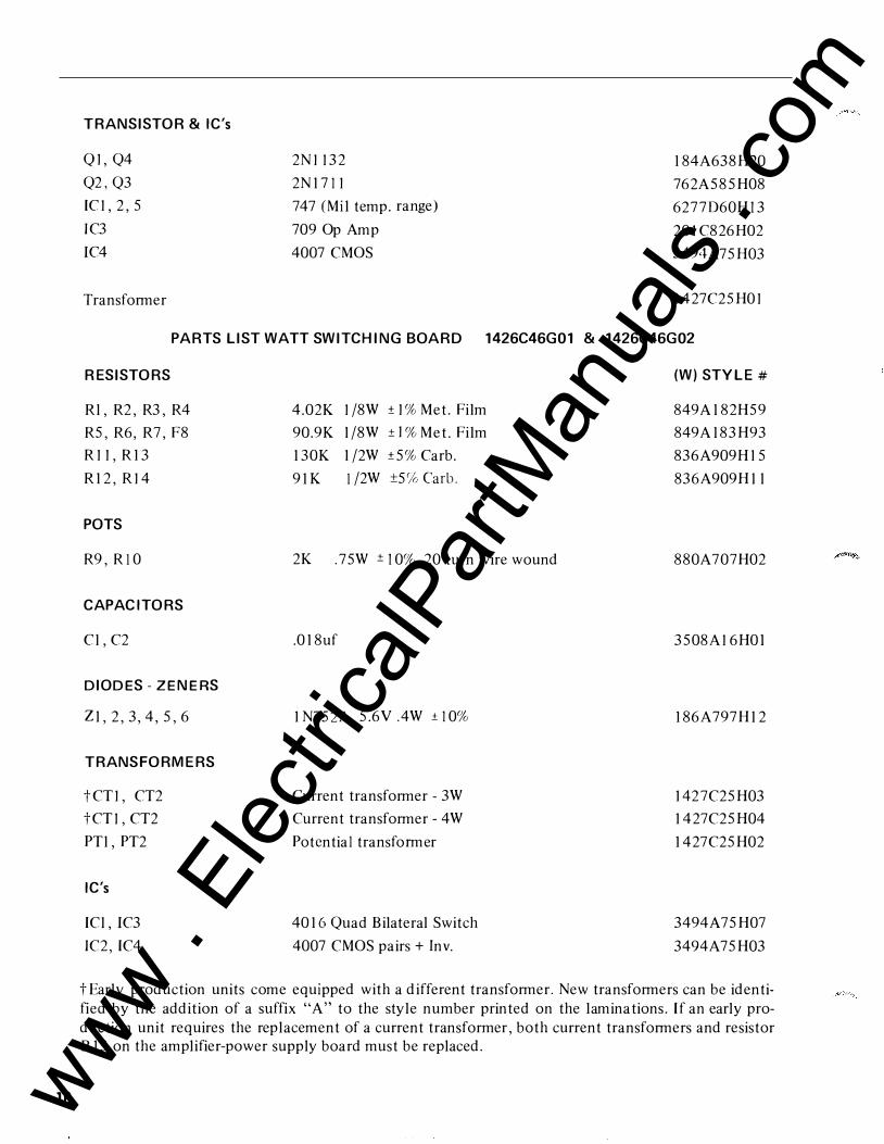
PARTS LIST ± 10% AMP. & POWER SUPPLY BOARD 1426C48G01
RESISTORS
Rl, R2, R9
R3,RS
R4
R6,R7
R8
RIO
Rl l,R12
R13
R14
RIS
R16
POT
R17
CAPACITORS
C 1 , C2, C 1 0, C 14
C3,C4
CS,C6,C7,C8,C9
C l l,Cl 2,C13
CIS
l.SKrl 1 /2W S% Ca rbon
10 Krl 1/8W 1% Met Film
82Srl 1/8W 1%Met Film
SOOrl SW ±S% Wi re wo und
82rl 1 /2W S% Ca rbon
33rl 1 /2W S% Ca rbon
27rl 1 /2W S% Ca rbon
36.SKrl 1 /8W 1% Met Film
24.3Krl 1 /8W 1% Met Film
18Krl 1 /2W S% Ca rbon
ISKrl 1 /2W S% Ca rbon
1 OK 1 W ± 1 0% wi re wo und 20 turn
.OOSmf 1 OOv d e Ce ramic
47 uf 3SV Tantalum
.1 uf 1 OOV Ce ramic
300uf 3V elect rolytic
.0047uf SOV Myla r
DIODES- ZENERS- BRIDGE
Zl, Z2 1 N966B .4W S% 16V
Z3 1 N82SA 6.2V ±S% Temp. Comp
Z4, ZS IN4747A 20V ±S% IW
Dl, 2,3,4,S,6, 7 1 N64SA
BR IOOV 1 amp b ri dge rect.
TRANSISTOR & IC's
Ql, Q4 2Nl l32
Q2, Q3 2N1711
ICI,IC2 747 (Mil temp range)
IC3 709 Op Amp
IC4 4007 CMOS
T ransfo rme r
(W) STYLE#
184A763H31
849A183HOI
849A181H89
762A679H04
184A763H01
187A290H13
187 A290H l l
849A183HSS
849A183H38
184A 763HS7
629AS31H60
880A 707HOI
184A663H13
184A661 H03
184A663H04
876A280H04
763A487Hl3
862A288HOS
862A288H06
849A487HOI
837A692H03
3S03A36HOI
184A638H20
762AS8SH08
627 7D60Hl3
201 C826H02
3494A7SH03
1427C2SHOI
Jfl"/'''�
www . El
ectric
alPar
tMan
uals
. com

I.L. 43-846.1A
PARTS LIST 0-110% AMP. & POWER SUPPLY BOARD 1531C02G01
RESISTORS
Rl, R2
R3,R5
R4
R6,R7
R8
R9
l.SK.Q
IOK.Q
825S1
400S1
82.Q
820S1
33.Q
27S1
1/2 w 5% Carb.
l/8W ± 1% Met. Film 50 ppmtC
1/8 W ± 1% Met. Film 50 ppmtC
SW ±5% Wire wound
I /2W ± 5% Car b.
I /2W ± 5% Car b.
I /2W ± 5% Car b.
1/2W ± 5% Carb.
RIO
Rl l,Rl2
Rl3 40.2KS1 l/8W ± l% MetFilm
Rl4
RIS
Rl6
Rl7
Rl8
R21
POTS
Rl9
R20
CAPACITORS
C1, C2, Cl 0, Cl4
C3,C4
C5,C6,C7,C8,C9
Cll ,Cl2,Cl3
CIS
DIODES- ZENERS- BRIDGE
Dl, 2,3,4,6, 7, 8,9
Zl, Z2
Z3
Z4,Z5
Z6,Z7
BR
24.3KS1 I /8W ± 1% Met. Film
18KS1 I /2W ± 5% Car b.
15KS1 l/2W ±5% Carb.
806S1 I /8W ± I% Met. Film
IK.Q I /2W ±5% Carb.
IK.Q I /8W ± I% Met. Film
I OK.Q .SW ± I 0% I turn cermet
kOK.Q .75W ± 10% 15 turn cermet
.005 mf I OOV de ceramic
47 mf 3SV tantalum
0.1 mf ceramic
300 mf 3V electrolytic
.0047mf mylar
1N645A
1N966B 16V .4W ±5%
I N825H 6.2V ± 5 tep1p comp.
l N4747A 20V I W
I N752A 5.6V .4W ± I 0%
I OOV, I amp bridge rect.
(W) STYLE#
184A763H31
849AI83HOI
849Al8IH89
763AI29Hl6
184A763HOI
184A763H25
187A290H13
187 A290Hl l
849A183H59
849A183H38
184A763H57
629A531H60
849AI81H88
184A763H27
849Al82H01
3504A61HOI
3504A60H01
l84A663Hl 3
184A661H03
184A663H04
876A280H04
763A487Hl3
837 A692H03
862A288H05
862A288H06
849A487HOI
186A797Hl2
3503A36HOI
9 www . El
ectric
alPar
tMan
uals
. com
10
TRANSISTOR & IC's
Q I, Q4 2N I I 32 184A638H20
Q2, Q3 2N 171 I 762A585H08
IC I, 2, 5 747 (Mil temp. range) 627 7D60H13
IC3 709 Op Amp 20 IC826H02
IC4 4007 CMOS 3494A75H03
Transformer 1427C25HO I
PARTS LIST WATT SWITCHING BOARD 1426C46G01 & 1426C46G02
RESISTORS
Rl, R2, R3, R4
R5,R6,R7,F8
R I I, R13
R12,R I 4
POTS
R9, RIO
CAPACITORS
Cl, C2
DIODES- ZENERS
Zl,2,3,4,5,6
TRANSFORMERS
tCT I, CT2
tCT I , CT2
PTl, PT2
IC's
ICl, IC3
IC2, IC4
4.02K I /8W ± I % Met. Film
90.9K l/8W ± I % Met. Film
130K 1/2W ±5% Carb.
91K I /2W ± 5% Carb.
2K . 7 5W ± 10% 20 turn wire wound
.018uf
1N752A 5.6V .4W ± 10%
Current transformer- 3W
Current transformer - 4W
Potential transformer
4016 Quad Bilateral Switch
4007 CMOS pairs+ lnv.
(W) STYLE#
849Al82H59
849Al83H93
836A909H15
836A909Hl l
880A707H02
3508A I 6H0 1
186A797Hl2
142 7C25H03
1427C25H04
1427C25H02
3494A75H07
3494A75H03
t Early production units come equipped with a different transformer. New transformers can be identified by the addition of a suffix "A" to the style number printed on the laminations. I f an early production unit requires the replacement of a current transformer, both current transformers and resistor R 13 on the amplifier-power supply board must be replaced.
www . El
ectric
alPar
tMan
uals
. com

I.L. 43-846.1A
PARTS LIST VAR SWITCHING BOARD 1427C."8G01 & 1427C48G02
RESISTORS
Rl, R2
R3,R4
R5,6, 7,8
Rl3, RlS
Rl4,Rl6
POTS
R9, 1 0, 1 1 , 12
CAPACITORS
Cl, C2, C3, C4
DIODES- ZENERS
Zl,2,3,4,5,6
TRANSFORMERS
*CTl, CT2
*CTl, CT2
PT I, PT2
IC's
ICI, IC2
IC3, IC4
7. 13K 1/SW ± 1% Met. Film
5.62K 1/SW ± 1% Met. Film
l .OM 1/SW ± 1% Met. Film
130K l/2W ±5% Carb.
9 1K l/2W ±5% Carb.
2K W± 10% wire wound 20 turn
.33uf SOY ±5% Poly Carb.
1N752A 5.6V 4W±l0%
Current Transformer - 3W
Current Transformer- 4W
Potential Transformer
40 16 Quad Bilateral Switch CMOS
4007 CMOS pair+ Inv.
(W) STYLE#
849Al 82H83
849A l82H73
849Al84H97
836A909Hl5
836A909H l l
880A707H02
863Al66Hl6
186A 797Hl 2
1427C25H03 1427C25H04
1427C25H05
3494A75H07
3494A75H03
*Early production units come equipped with a different transformer. New transformers can be identified by the addition of a suffix "A" to the style number printed on the laminations. If an early production unit requires the replacement of a current transformer, both current transformers and resistor Rl3 on the amplifier-power supply board must be replaced.
1 1 www . El
ectric
alPar
tMan
uals
. com
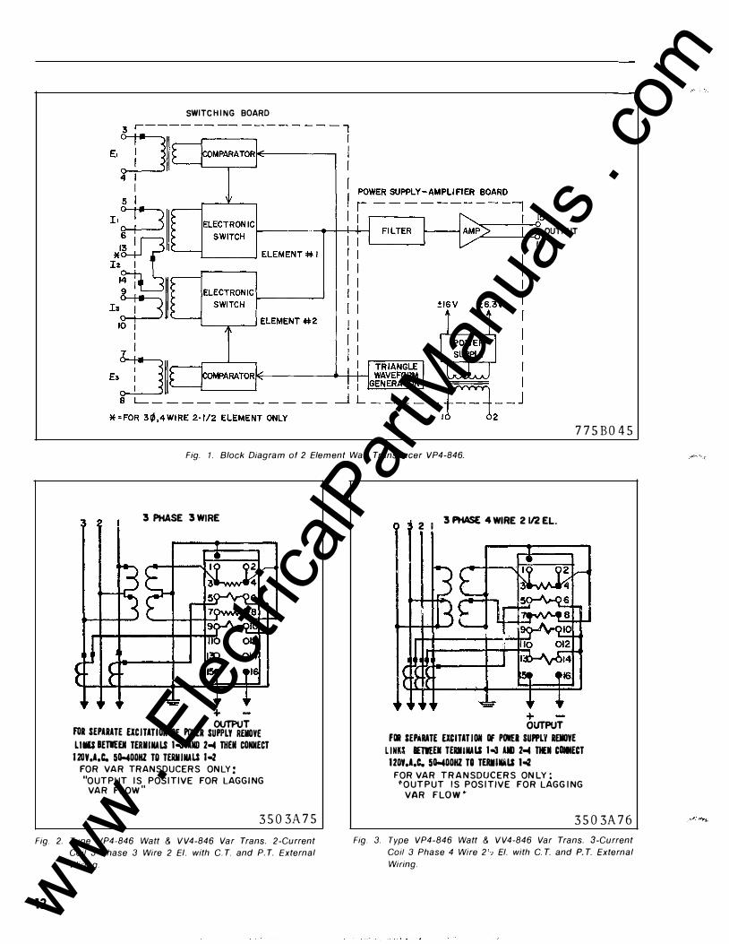
SWITCHING BOARD
15 OUTPUT
16
775B045
Fig. 1. Block Diagram of 2 Element Watt Transducer VP4-846.
3 PHASE 3 WIRE
+ OUTPUT
FOR SEPARATE EXCITATION OF POWER SUPPLY REMOVE
LilliS B£11££11 TERMINALS 1-.1 ANO 2-4 THEN CONNECT
J20V.A.C. 50-400HZ TO TERMINALS J.Z FOR VAR TRANSDUCERS ONLY! "OUTPUT IS POSITIVE FOR LAGGING
VAR FLOW"
350 3A 75
Fig. 2. Type VP4-846 Watt & VV4-846 Var Trans. 2-Current
Coil 3 Phase 3 Wire 2 El. with C. T. and P. T. External
Wiri11g.
12
2 1 3 PHASE 4 WIRE 2 112 EL.
+ OUTPUT
FOR SEPaRATE EXCITATION OF POWEI SUPPLY REIIOV£
LINK$ 8ETIEEII TERIIINALS 1-.1 Alii 2-4 THEil CDIIIECT
120Y.A.C. 50-400HZ TD TERIIIIiLS 1-2
FOR VAR TRANSDUCERS ONLY: �OUTPUT IS POSITIVE FOR LAGGING
VAR FLow•
350 3A 76
Fig. 3. Type VP4-846 Watt & VV4-846 Var Trans. 3-Current
Coil 3 Phase 4 Wire 2 '2 El. with C. T. and P. T. External
Wiring.
www . El
ectric
alPar
tMan
uals
. com

3PH. 3 WIRE V P 4- 846 WATT TRANSDUCER 3PH. 3WIRE VV4-846 VAR TRANSDUCER
SINGLE P HASE TEST CONNECTIONS
E +
+ I
+ OUTPUT
SEPARATE 120 V A C EXCITATION FOR THE POWER SUPPLY TER MINALS 1-2 MAY BE PROV IDED OR THE JUMPERS USED AS SHOWN
3515A 35
Fig. 4. Single Phase Test Conn., 3¢ 3W.
J.L. 43-846.1 A
3 PH. 4 WIRE 2112 EL. VP4-846 WATT TRANSDUCER
3 PH 4 WIRE 21/2 EL. V V4-846 VAR. TRANSDUCER
SINGLE PHASE TEST CONNE CTIONS
E +
+ -I
+ OUTPUT
SEPARATE 120VAC EXCITATION FOR THE POWER SUPPLY TER MINALS 1-2 MAY BE PROV I DED OR THE JUMPERS USED AS SHOWN.
3515A36
Fig. 5. Single Phase Test Conn. , 3D 4W 2'/:z El.
ELEMENT I ELEMENT 2 OUTPUT PHASE
Gl PI 0 0
PHASE
P2 0
BOTTOM VIEW
G2 0
Fig. 6. Var Transducer Individual Element Adjustments.
TERMIN AL # 15 ON TOP PANEL AT THIS END.
351SA6 1
13 www . El
ectric
alPar
tMan
uals
. com

.... ..
. 2 50±.010J �-------- 5.250:!:.010
l 5.750±.015---------�
.218 DIA (4 HOLES) FOR MOUNTING
3.000 MAX .
4.875
LINE NO. I 2 3 4 5
+-1 ' t
TYPE (LATER)
VP4-846 VP4-846 W4-846
VV4-846
I
--�" "'"" I I�
D RI L LING P LAN ' 1 5� �
TRANSDUCER TYPE TERMINAL IN POS ITION N UMBER TERM SCREWS
3 WIRE 2 C. C. WATT 1-2-3-4· 5- 6·7-8·9 -10-15-16 .164-32 4 WIRE 3C.C. WATT 1-2·3·4·5·6·7-8·9·10 -13-14-15-16 .164-32 3 WIRE 2 C.C. VAR. 1·2·3·4· 5-6-7-8-9-1 0-15·16 .164- 32 4 WIRE 3 C. C. VAR 1·2·3·4 5·6 ·7·8·9·10 ·13 14-15-16 164-�
1428C2 3
Fig. 7. Outline and Dwg. VP4 & VV-846 Transducer in 3 inch case.
www . El
ectric
alPar
tMan
uals
. com

COMPARATOR INPUT VOLTAGE SIG. OFF
-
NPN (2NI711)
COMPARATOR INPUT VOLTAGE SIG. ON
FOR BOTH OHMMETER POLARITIES
FOR BOTH OHMMETER POLARITIES
PNP (2NII32)
Fig. B. Transistor Checking.
FOR BOTH OHMMETER POLARITIES
I.L. 43-846.1A
3515A 37
_P_C:7743�=-
r-------------------.-------���----------------�--------6���44�-'--� ������·� i.,woc 4*' '
631 i36 ....---------------+--------?>:1-- "'""=1 TRIANGLE WAVE
I
'GENERATOR
IIG·, I s-*11
M ls6 ....----------------=--.__ _______________ +--------7· -<E-- -6.3\!DC roc 62\ 126
SIGNAL OUT �--r--611 116 �--------------------------------------------------------------------------_.------�: <E--COMM�
I I su��� li'�TERMINAL BLOCK NUMBERS. �=PRINTED CKT. BOARD IDENTIFICATION. l!l•3W USE .012MFD
4W USE .015 MFD
VAC • 0.0 :Xa4A.
OUTPUT•I.ONA
Fig. 9. Switching Bd., VP4-846 Watt Transducer (3(/. 3W, 2 El.
& 3ft. 4 W, 2 '< El.).
774B6 5 3
15 www . El
ectric
alPar
tMan
uals
. com

16
COMPARATOR JNPUT VOLTAGE SIG Off
-
[ill] 0 0
COMP. DESCRIP TION
lCI ,IC3 4016
ICZ ,1C4 4007
8 "' " u "' N :!:
0 0
CIRCUIT SCOPE APPLICATION POINTS*
COMPARATOR INPUT lC2 a IC 4 PIN 10 a COMMON
INVERTER INPUT IC2 a IC4 PIN 8 a COMMON INVERTER OUTPUT IC2 a lC4 PIN I a COMMON CURRENT TRANSFORMER ICI a IC3 PIN Sia4 SECONDARY
PULSE SHAPER INPUT IC2 a IC4 PIN6 a COMMON
DC OUTPUT OF SWITCH lCI a lC3 PIN 3 a COMM ON
lf= SEE SC HEMATIC FOR WAVE FORMS
3514ASO
Fig. 10. Component Location -Switching Bd. Watt Transducer.
COMPARATOR JNR.JT VOLTAGE SJG. ON P. C. 80. 7748655 REF
---�-�
.:,MFO RE
D IJG� II
+• >VOC
� � 120V a:: N P T2
�YELLOW ! �� �� .63 3.6 �--------------�----�--�
TRIANGLE! WAVE
GENERA-YEUDW * TOR �.--l�f---1*-.IE:, .
4JlD_. _ _..., RED .65 �--��••v
.61 1.6
lDC �2� 12.6-DC SIGNAL OUT ,-,�
�--------------�-, .-o
-.o
--------------------------------------------------------------------·
---�---___j--�.--�00
z�4A. VACs 120 PWR * :TERMINAL BLOCK NUMBERS I�4.2A SUPPLY .6 • PRINTED CKT. BOARD IDENTIFICATION. EQUAL
MARKSPACE OUTPUT<OO
UNEQUAL hiARKED-SPACE OUTPUT•IOMA
Fig. 1 1. Switching Bd., VV4-846 Var Transducer (3(/. 2W, 2 El.
& 3rl, 4fJ, 2'z E/).
774B654
www . El
ectric
alPar
tMan
uals
. com
ll<15
*•TERMINAL BLOCK NUMBERS.
-6.3V
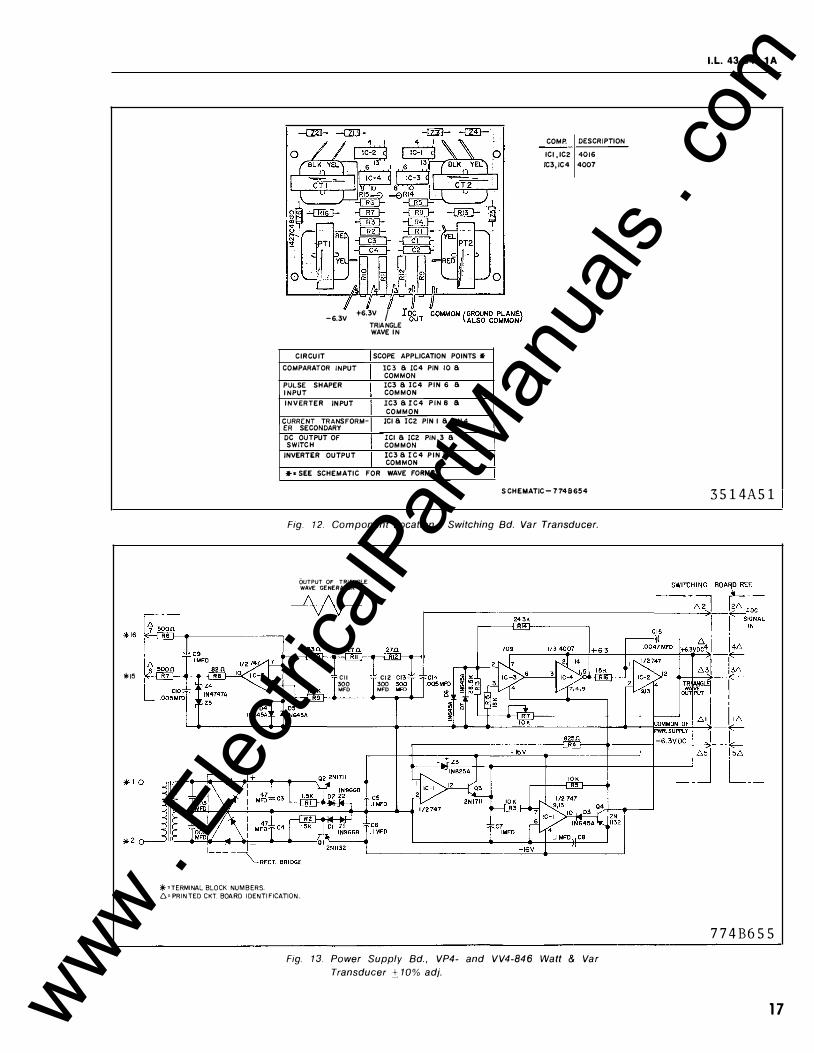
CIRCUIT
COMPARATOR INPUT
PULSE SHAPER INPUT
IN V ER TER INPUT
+6.3V I TRIANGLE WAVE IN
SCOPE APPLICATION POINTS ll' IC3 a IC4 PIN 10 a COMMON
IC3 a !C4 PIN 6 a COMMON
lC3 a IC4 PIN 8 a
COMMON
CURRENT TRANSFORM- ICI a ICZ PIN I a PIN4 ER SECONDARY
DC OUTPUT OF ICI a ICZ PIN 3 a SWITCH COMMON
INVERTER OUTPUT IC3 a IC4 PIN I a COMMON
ll'• SEE SCHEMATIC FOR WAVE FORMS
COMP. DESCRIPTION
ICI ,IC2 4016
fC3,1C4 4007
S CHEMATIC-7748654
Fig. 12. Component Location - Switching Bd. Var Transducer.
OUTPUT OF TRIANGLE WAVE 'GENERATOR
Cll Cl2 300 300 MFO MFD
6• PRINTED CKT BOARD IDENTIFICATION.
Fig. 13. Power Supply Bd., VP4- and VV4-846 Watt & Var
Transducer ± 10% adj.
I.L. 43-846.1A
3514A51
774B6 55
17 www . El
ectric
alPar
tMan
uals
. com

18
,--! A 4oon
"''" �� ·� i!.i 1 1 400!1
.. .. l
RG
� N
Jl Jl
± 6.3/ I DC /SIG. \ +�.3V. �.3V. COMMON IN �· �-TRIANGLE
WAVE OUT
CIRCUIT SCOPE A PPLICATION POINTS * TRIANGLE WAVE CABLE 'fl'3 BOA R D EDGE TO COMMON, OUTPUT CABLE"*I BOARD EDGE.
if= SEE SCHEMATIC FOR WAVE FORMS.
COMP. DESCRIPTION
QI,Q4 2NII32
Q2,Q3 2NI711
ICI,IC2 747 IC 3 709
IC4 4007
NOTE: COLLECTORS OF THE 2NI711 a 2NII32 ARE CONNECTED TO THE TRANSISTOR CASE.
3514A52
Fig. 14. Component Location - Power Supply Bd.- ±10% adj.
OUTPUT OF TRIANGLE WAVE GENERATOR SWITCHING BOARD REF. 1\ 1\ v v
+16.6V 24.3K Rl4
27!l 27!l II
Cl2 Cll Cl4
---� �--I <E--Ioc
I SIGNAL
Cl5 IN
b.' j. L; +6.3YOC4 1 <(---13l; .,.___
300 300 MAl MFU I I
I·L> <C--
L !"-"' __ ] L __ -fitr--<
:; '-Uill-... �1-+t-. cs M� ::Sr-+'::..::;.-*""-+--+-----+-t--+--1
:; rlJID-�Hf+oil...l cs
.if 2 o-----3 L_---=---l'l--*i-::-__.-�:c:-' ,"'--+-_.�FD
*=TERMINAL BLOCK NUMBERS. !:::,.=PRINTED CKT. BOARD IDENTIFICATION.
01, 02,08, 09 (IN645A) ZI,Z2 {IN9668)
Fig. 15. Power Supply Bd., VP4- and VV4-846 Watt & Var
Transducer with 0-110% adj. amplifier.
774B844
www . El
ectric
alPar
tMan
uals
. com

g ---1,--� 'C - ---u t{') '¢
0
6.3 VDC Ioc SIGNAL
IN
ZERG ADJ.
747 ICI 038
I ,... __ .....;� ___ .J
04 05 TRIANGLE +6.3V -6.3V
WAVE OUT
I
Fig. 16. Component Location Power Supply Bd. 0-110% adj.
I.L. 43-846.1!
6
0
775B482
19 www . El
ectric
alPar
tMan
uals
. com

WESTINGHOUSE ELECTRIC CORPORATION RELAY-INSTRUMENT DIVISION NEWARK, N. J.
Printed in U.S.A. www . El
ectric
alPar
tMan
uals
. com