Embed Size (px)
Citation preview
1
ELEC 6740 Electronics Manufacturing
Chapter 9: Solder Paste and Its Application
R. Wayne JohnsonAlumni Professor
Auburn University334-844-1880
Outline1. Introduction2. Solder Paste Properties3. Solder Paste Printing Equipment4. Solder Paste Printing Processes5. Paste Printing Defects6. Paste Printing Variables7. Printing for Different Types of Components
Introduction
! Solder paste printing is a critical step in the SMT process– Solder paste– Printers– Process– Defects
2
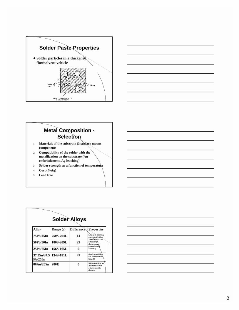
Solder Paste Properties
! Solder particles in a thickened flux/solvent vehicle
Metal Composition -Selection
1. Materials of the substrate & surface mount components
2. Compatibility of the solder with the metallization on the substrate (Au embrittlement, Ag leaching)
3. Solder strength as a function of temperature4. Cost (%Ag)5. Lead free
Solder Alloys
Highest quality for Au surfaces: die attachement & closures
0280E80Au/20Sn
Good wettability, not recommended for gold
47134S-181L37.5Sn/37.5Pb/25In
9156S-165L25Pb/75In
29180S-209L50Pb/50In
Less gold leaching, more ductile than Sn/Pb alloys: Die attachment, closures, and general circuit assembly
14250S-264L75Pb/25In
PropertiesDifferenceRange (c)Alloy
3
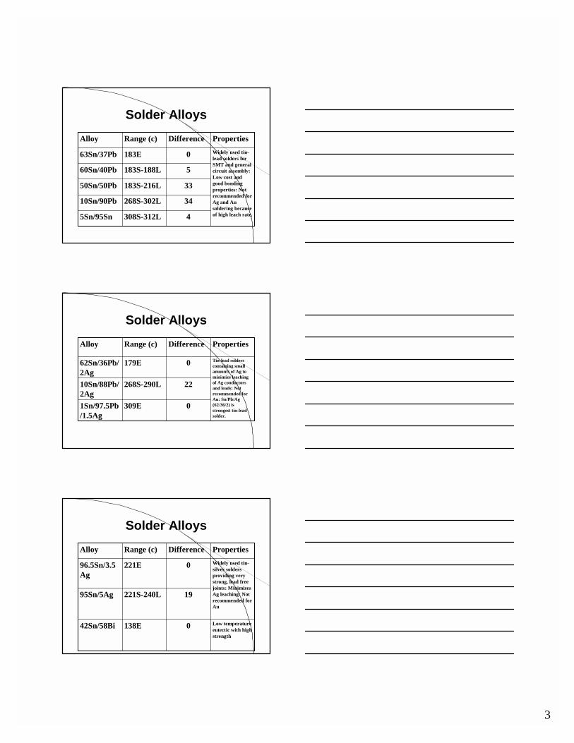
Solder AlloysPropertiesDifferenceRange (c)Alloy
4308S-312L5Sn/95Sn
34268S-302L10Sn/90Pb
33183S-216L50Sn/50Pb
5183S-188L60Sn/40Pb
Widely used tin-lead solders for SMT and general circuit assembly: Low cost and good bonding properties: Not recommended for Ag and Au soldering because of high leach rate.
0183E63Sn/37Pb
Solder AlloysPropertiesDifferenceRange (c)Alloy
0309E1Sn/97.5Pb/1.5Ag
22268S-290L10Sn/88Pb/2Ag
Tin-lead solders containing small amounts of Ag to minimize leaching of Ag conductors and leads: Not recommended for Au: Sn/Pb/Ag (62/36/2) is strongest tin-lead solder.
0179E62Sn/36Pb/2Ag
Solder AlloysPropertiesDifferenceRange (c)Alloy
Low temperature eutectic with high strength
0138E42Sn/58Bi
19221S-240L95Sn/5Ag
Widely used tin-silver solders providing very strong, lead free joints: Minimizes Ag leaching: Not recommended for Au
0221E96.5Sn/3.5Ag
4
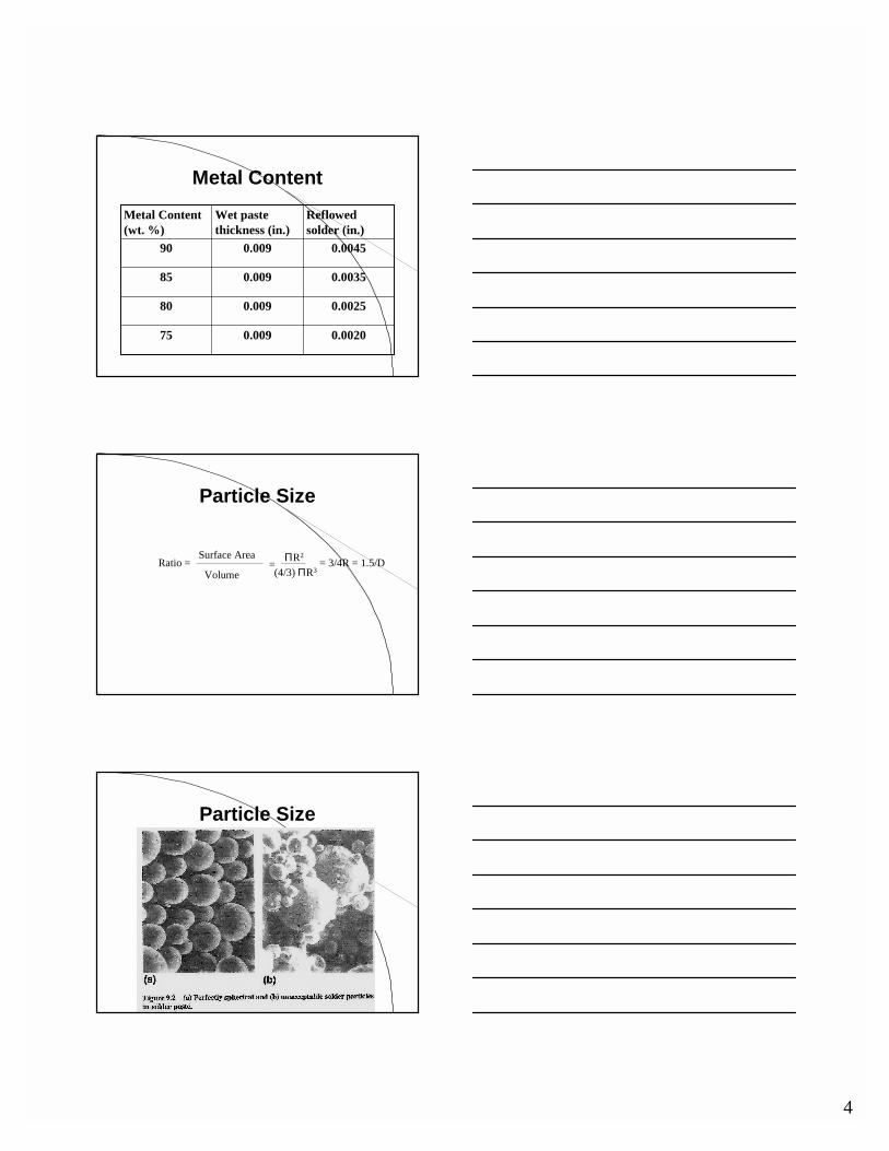
Metal Content
0.00200.00975
0.00250.00980
0.00350.00985
0.00450.00990
Reflowed solder (in.)
Wet paste thickness (in.)
Metal Content (wt. %)
Particle Size
Ratio = Surface Area
Volume= ΠR2
(4/3) ΠR3= 3/4R = 1.5/D
Particle Size
5
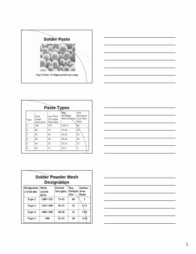
Solder Paste
Type 3 Paste: 25-45µµµµm particle size range
Paste Types
515-515206
1525-1525305
2038-2038404
2045-2545503
2075-4575802
20150-751501601
10% Maximum Less Than (um)
80% Minimum Between (um)
Less Than 1% Larger Than (um)
None Larger Than (um)
Type
Solder Powder Mesh Designation
3.331825-15-500Type 5
1.933138-20-400/+500Type 4
1.713545-25-325/+500Type 3
16075-45-200/+325Type 2
Surface Area Ratio
Ave. Particle Size
Particle Size (µµµµm)
MeshASTM B214
DesignationJ-STD-005
6
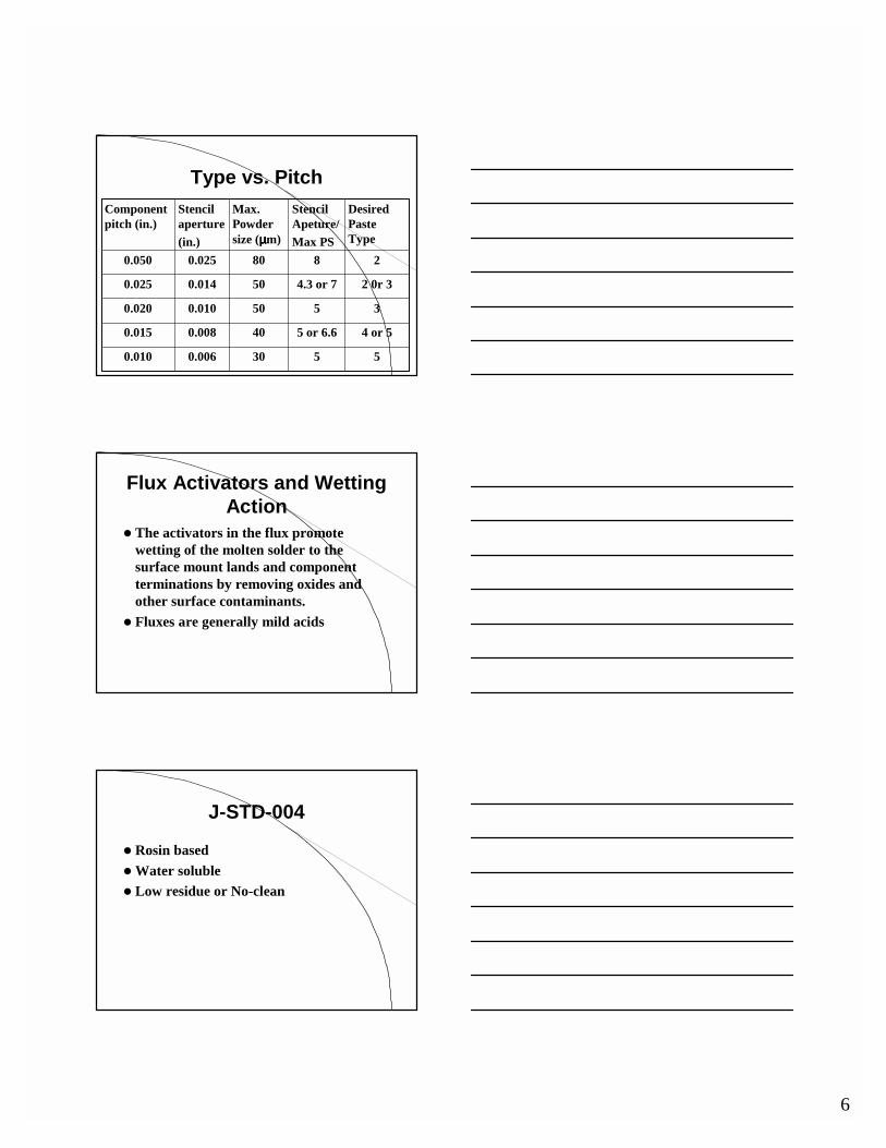
Type vs. Pitch
55300.0060.010
4 or 55 or 6.6400.0080.015
35500.0100.020
2 0r 34.3 or 7500.0140.025
28800.0250.050
Desired Paste Type
Stencil Apeture/Max PS
Max. Powder size (µµµµm)
Stencil aperture(in.)
Component pitch (in.)
Flux Activators and Wetting Action
! The activators in the flux promote wetting of the molten solder to the surface mount lands and component terminations by removing oxides and other surface contaminants.
! Fluxes are generally mild acids
J-STD-004
! Rosin based! Water soluble! Low residue or No-clean
7
Rosin
! Rosin flux is primarily composed of natural resin extracted from the oleoresin of pine trees and refined.– Rosin (R)– Rosin, mildly activated (RMA)– Rosin activated (RA)
! Rarely used, very high activity level
Water Soluble
! Organic acids (OA)! Must be cleaned after soldering! Formulated with a glycol base
No-clean
! Natural resins other than rosin types and/or synethic resins
! Varying ‘solids’ content– Impacts amount of flux residue– Some leave no visible residue
! Residue is non-corrosive, non-conductive and can be left on the board
8
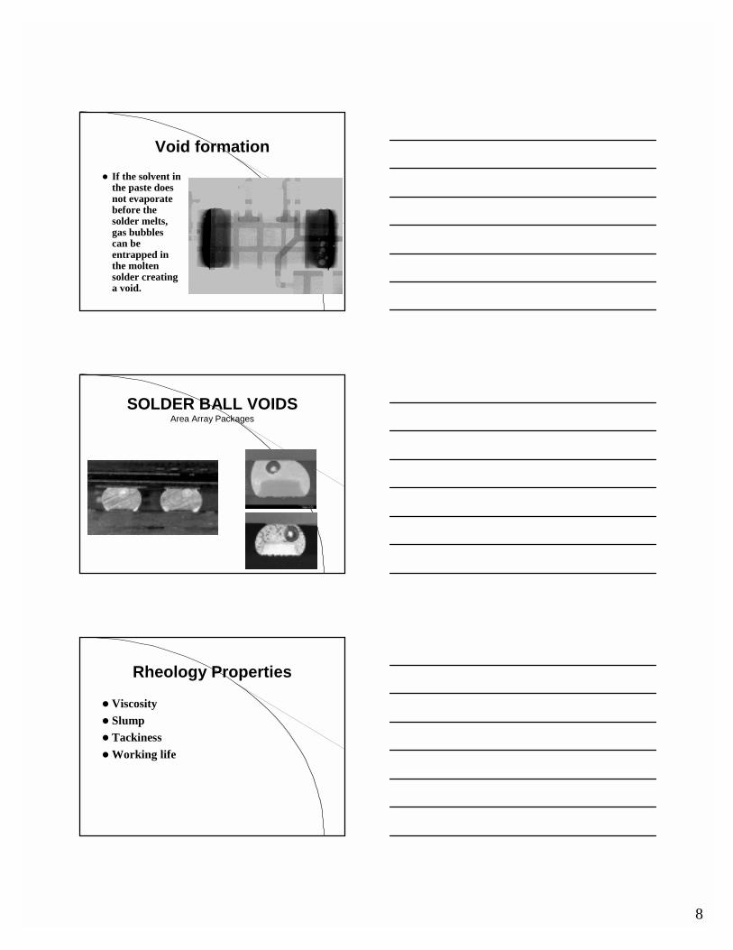
Void formation! If the solvent in
the paste does not evaporate before the solder melts, gas bubbles can be entrapped in the molten solder creating a void.
SOLDER BALL VOIDSArea Array Packages
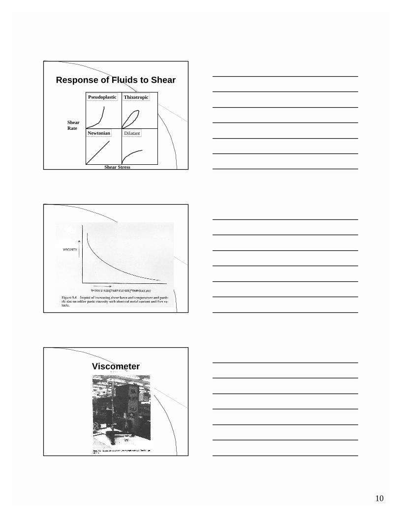
Rheology Properties
! Viscosity! Slump! Tackiness! Working life
9
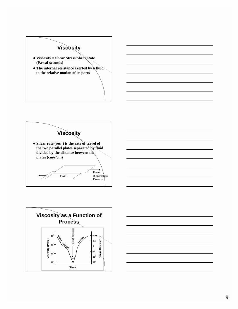
Viscosity
! Viscosity = Shear Stress/Shear Rate (Pascal-seconds)
! The internal resistance exerted by a fluid to the relative motion of its parts
Viscosity
! Shear rate (sec-1) is the rate of travel of the two parallel plates separated by fluid divided by the distance between the plates (cm/s/cm)
Force(Shear stressPascals)
Fluid
Viscosity as a Function of Process
102
103
104
105
Visc
osity
(Poi
se)
Time
Stirring
Squeegee
Thr
ough
the
scre
en
Leveli
ng
103
102
10
1
0.1
0.01
Shea
r R
ate
(sec
-1)
10
Newtonian
Pseudoplastic Thixotropic
Dilatant
Response of Fluids to Shear
Shear Stress
ShearRate
Viscometer
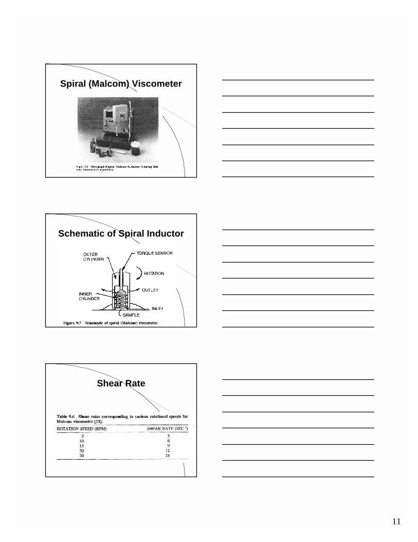
11
Spiral (Malcom) Viscometer
Schematic of Spiral Inductor
Shear Rate
12
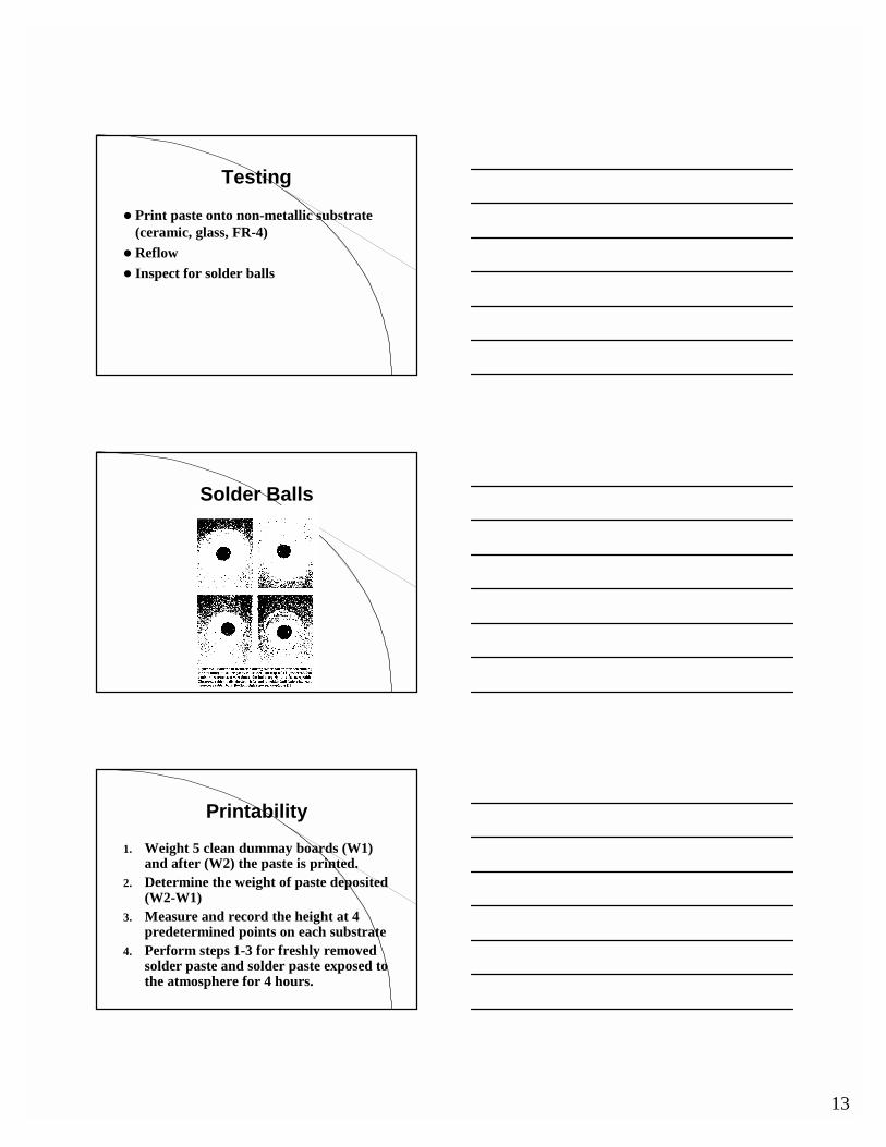
Solder Balls1. Solder balls are formed by very fine powder
particles in the solder paste.! They are carried away from the main solder
deposit as the flux melts and flows before the solder itself melts.
! This happens especially when the paste is deposited outside the land area either by design or misregistration
! These smaller particles lose contact with the larger solder paste deposit and when the solder melts, each particle becomes a small solder ball at the periphery of the original paste deposit
! A collectionm opf small solder balls around the main solder deposit is called a ‘halo’.
Solder Balls2. Solder balls are also formed when the oxide
layer on the nsurface of the solder powder particles is so thick the flux and any activator in the paste are not sufficient to remove it.
! Since the oxide cannot melt at soldering temperatures, they are pushed aside as a solder ball by the surrounding oxide-free molten solder.
! Solder balls formed in this manner are larger than those formed by the 1st mechanism because of the presence of surface oxide which is less dense than the metal.
Solder Balls
! Improper handling! Excessive baking/preheat prior to reflow! Particle rubbing (Fretting corrosion)! No-clean more likely to have solder balls
– Less aggressive flux
13
Testing
! Print paste onto non-metallic substrate (ceramic, glass, FR-4)
! Reflow! Inspect for solder balls
Solder Balls
Printability
1. Weight 5 clean dummay boards (W1) and after (W2) the paste is printed.
2. Determine the weight of paste deposited (W2-W1)
3. Measure and record the height at 4 predetermined points on each substrate
4. Perform steps 1-3 for freshly removed solder paste and solder paste exposed to the atmosphere for 4 hours.
14
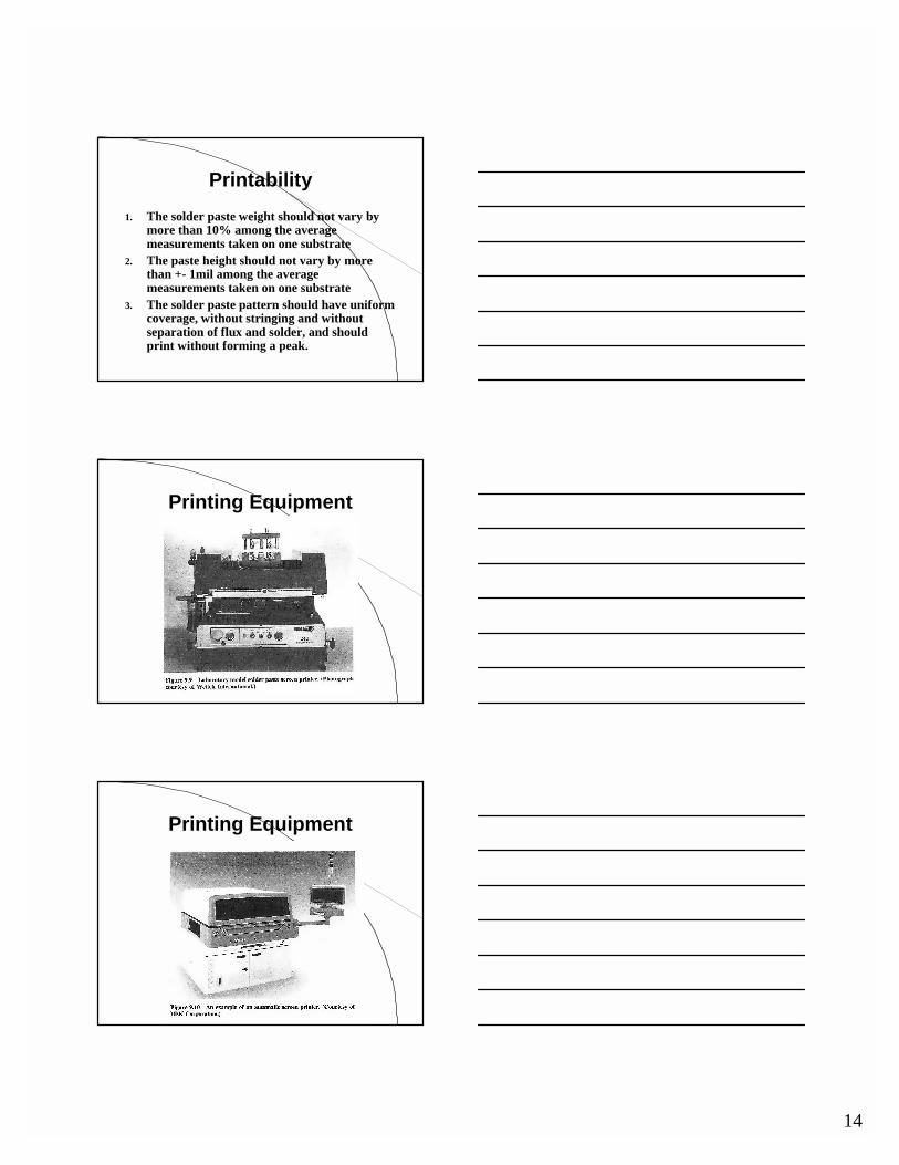
Printability1. The solder paste weight should not vary by
more than 10% among the average measurements taken on one substrate
2. The paste height should not vary by more than +- 1mil among the average measurements taken on one substrate
3. The solder paste pattern should have uniform coverage, without stringing and without separation of flux and solder, and should print without forming a peak.
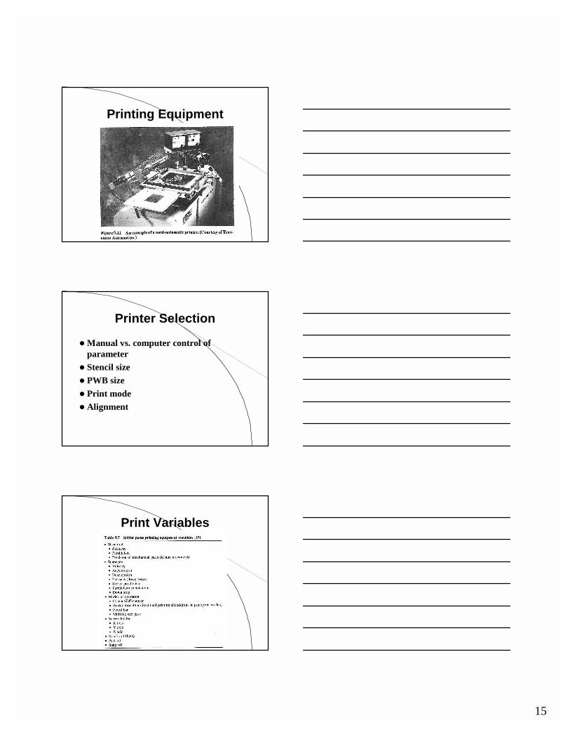
Printing Equipment
Printing Equipment
15
Printing Equipment
Printer Selection
! Manual vs. computer control of parameter
! Stencil size! PWB size! Print mode! Alignment
Print Variables
16
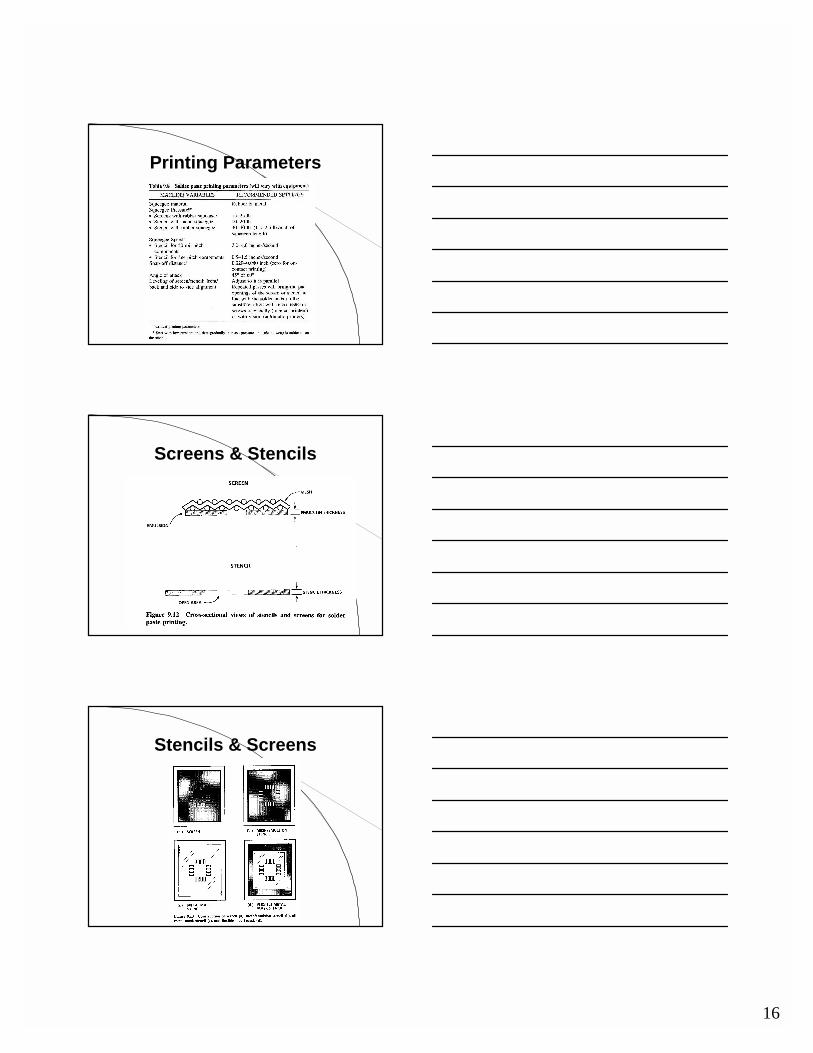
Printing Parameters
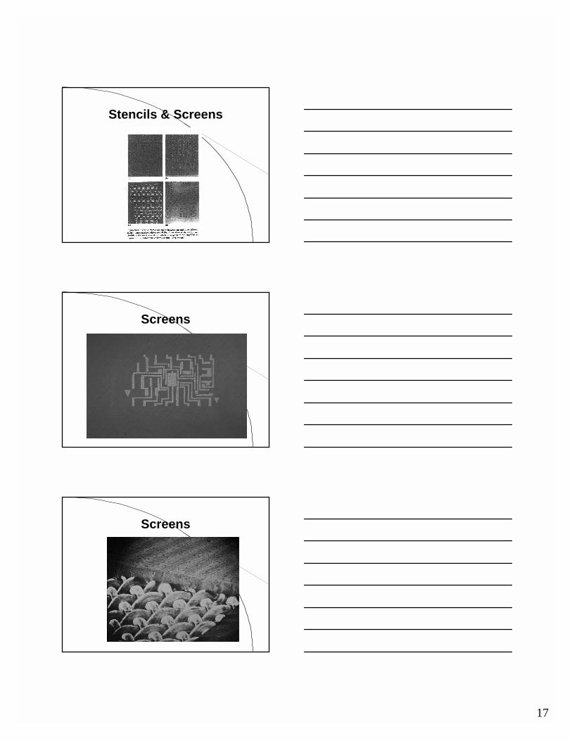
Screens & Stencils
Stencils & Screens
17
Stencils & Screens
Screens
Screens
18
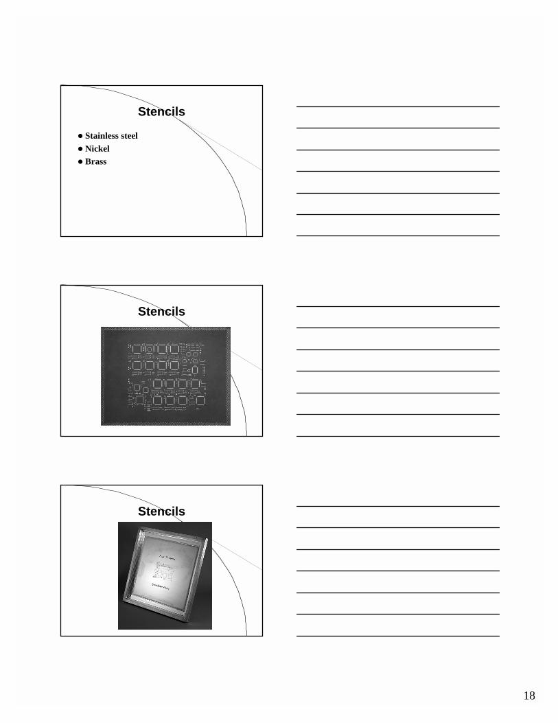
Stencils
! Stainless steel! Nickel! Brass
Stencils
Stencils
19
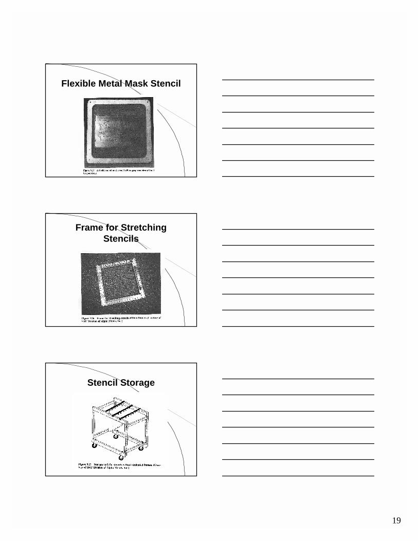
Flexible Metal Mask Stencil
Frame for Stretching Stencils
Stencil Storage
20
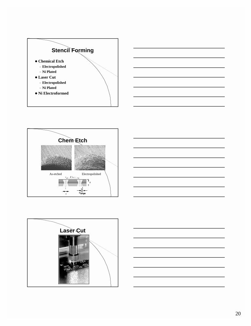
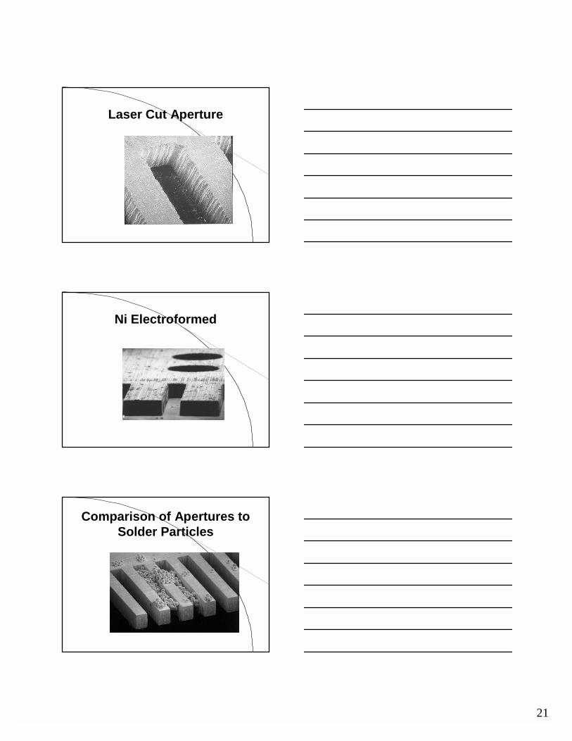
Stencil Forming
! Chemical Etch– Electropolished– Ni Plated
! Laser Cut– Electropolished– Ni Plated
! Ni Electroformed
Chem Etch
As-etched Electropolished
Laser Cut
21
Laser Cut Aperture
Ni Electroformed
Comparison of Apertures to Solder Particles
22
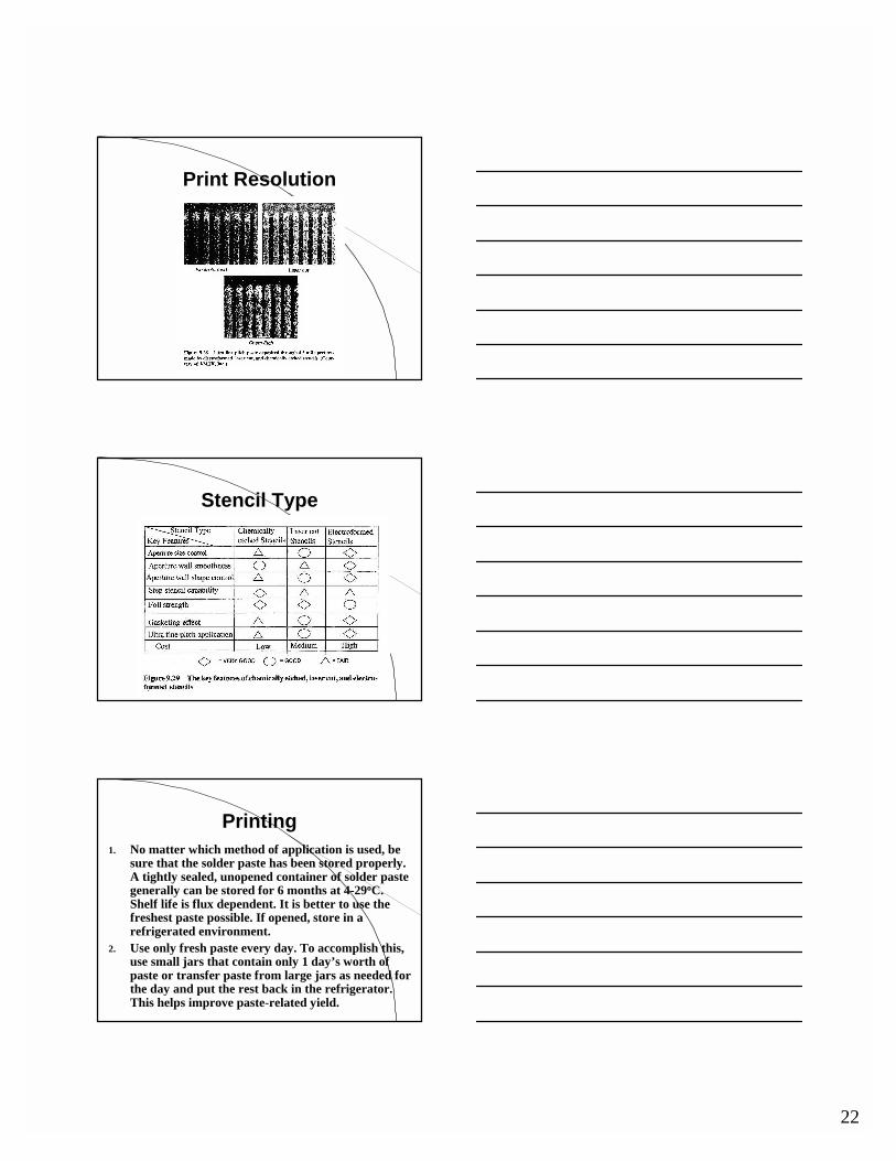
Print Resolution
Stencil Type
Printing1. No matter which method of application is used, be
sure that the solder paste has been stored properly. A tightly sealed, unopened container of solder paste generally can be stored for 6 months at 4-29oC. Shelf life is flux dependent. It is better to use the freshest paste possible. If opened, store in a refrigerated environment.
2. Use only fresh paste every day. To accomplish this, use small jars that contain only 1 day’s worth of paste or transfer paste from large jars as needed for the day and put the rest back in the refrigerator. This helps improve paste-related yield.
23
Printing3. Allow refrigerated container to reach room
temperature before use. It may ber advisable to take the paste out of the refrigerator the night before for the next day’s use to avoid the wait.
4. Check the solder paste for solder ball characteristics and viscosity.
5. When all solder paste printing is complete, wash the screen or stencil with the appropriate solvents.
6. Discard (hazardous material) any used paste.
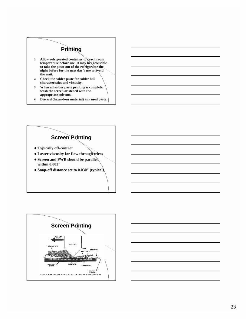
Screen Printing
! Typically off-contact! Lower viscosity for flow through wires! Screen and PWB should be parallel
within 0.002”! Snap-off distance set to 0.030” (typical)
Screen Printing
24
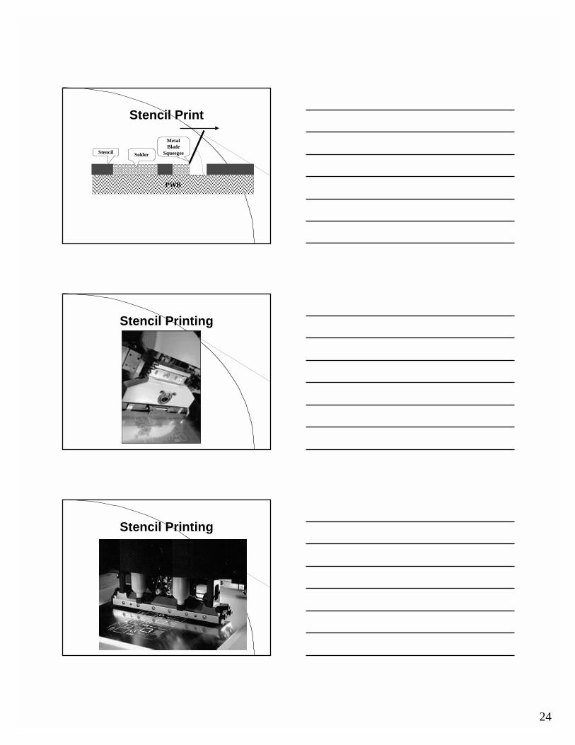
Stencil Print
PWB
Stencil Solder
MetalBlade
Squeegee
Stencil Printing
Stencil Printing
25
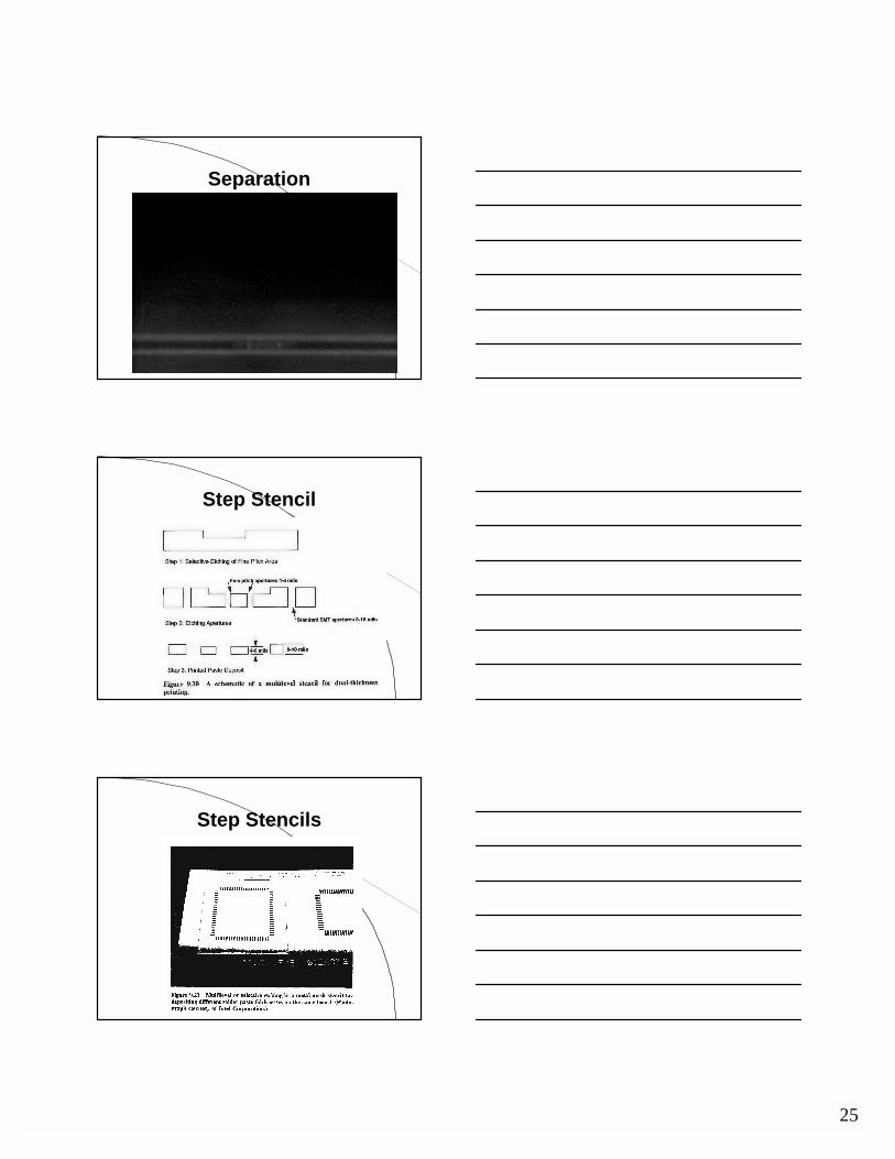
Separation
Step Stencil
Step Stencils
26
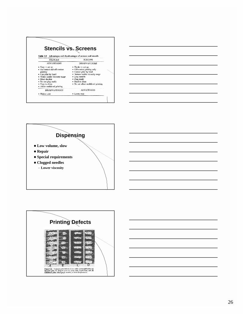
Stencils vs. Screens
Dispensing
! Low volume, slow! Repair! Special requirements! Clogged needles
– Lower viscosity
Printing Defects
27
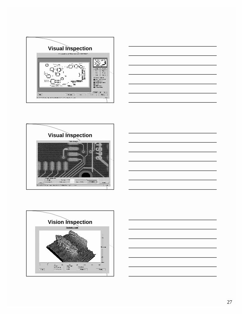
Visual Inspection
Visual Inspection
Vision Inspection
28
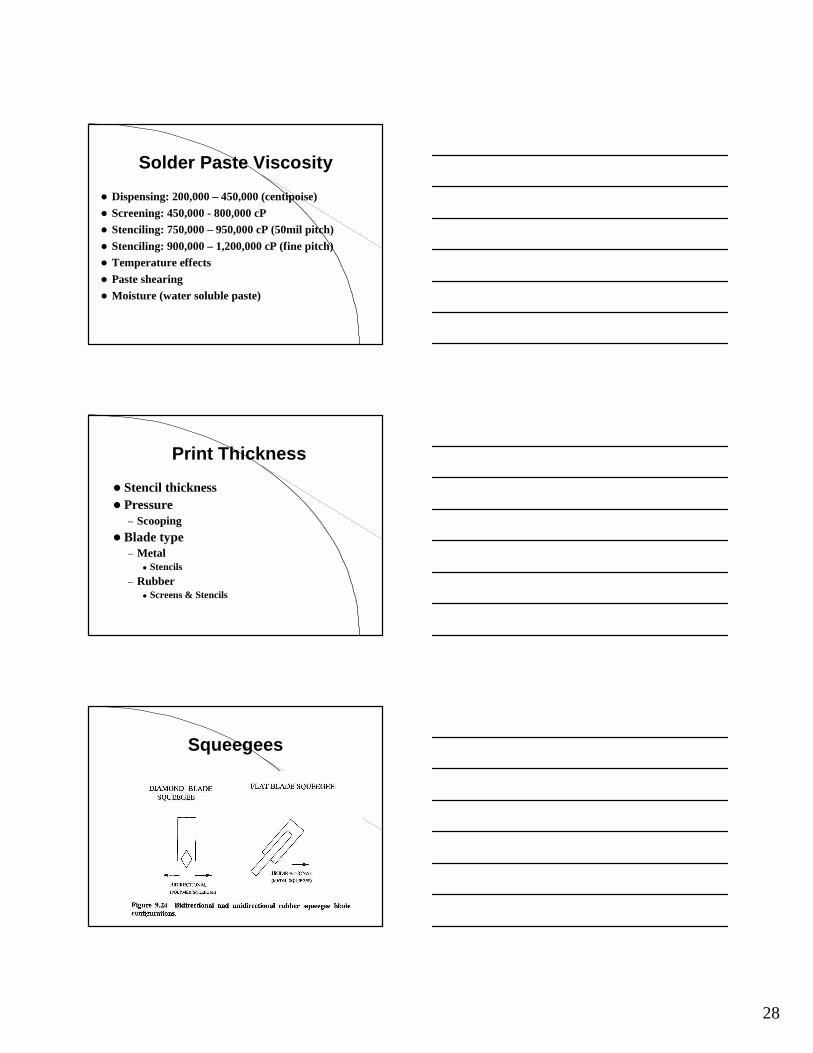
Solder Paste Viscosity! Dispensing: 200,000 – 450,000 (centipoise)! Screening: 450,000 - 800,000 cP! Stenciling: 750,000 – 950,000 cP (50mil pitch)! Stenciling: 900,000 – 1,200,000 cP (fine pitch)! Temperature effects! Paste shearing! Moisture (water soluble paste)
Print Thickness! Stencil thickness! Pressure
– Scooping! Blade type
– Metal! Stencils
– Rubber! Screens & Stencils
Squeegees
29
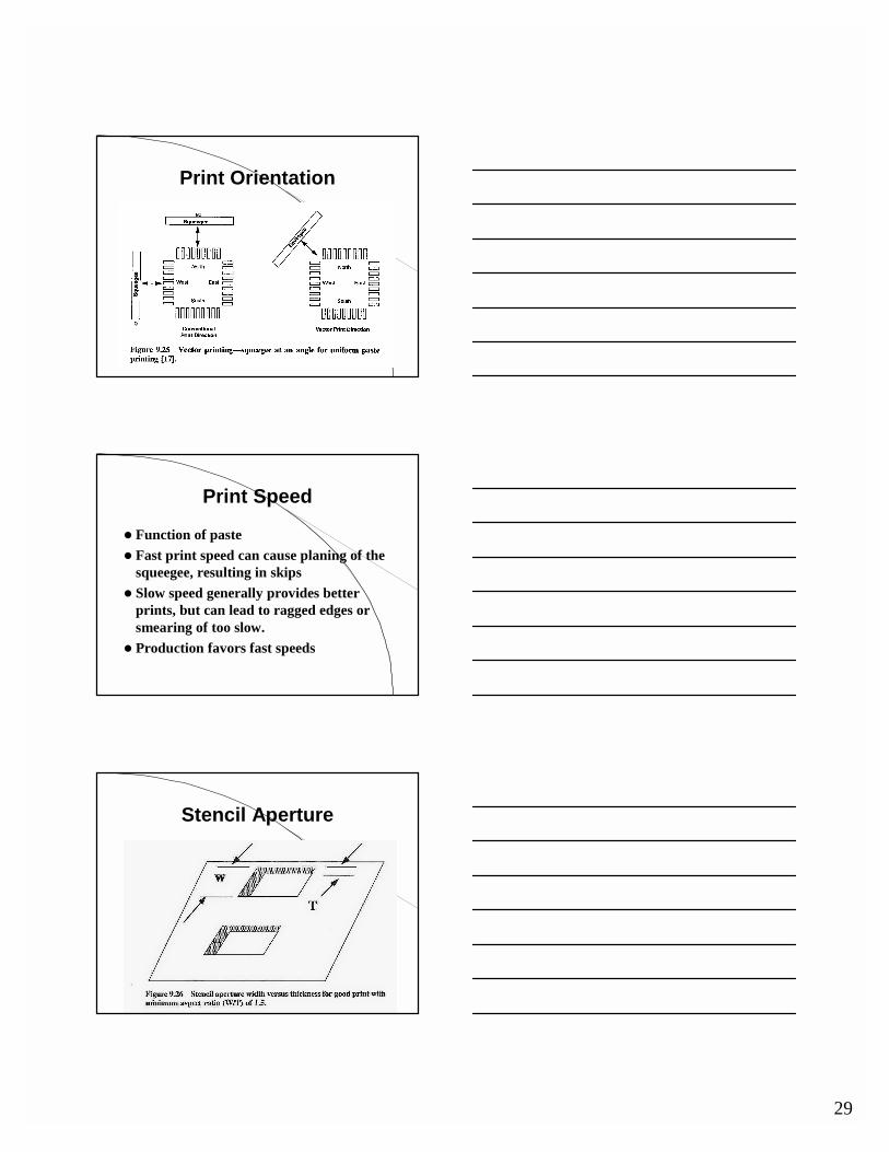
Print Orientation
Print Speed
! Function of paste! Fast print speed can cause planing of the
squeegee, resulting in skips! Slow speed generally provides better
prints, but can lead to ragged edges or smearing of too slow.
! Production favors fast speeds
Stencil Aperture
30
Print Thickness
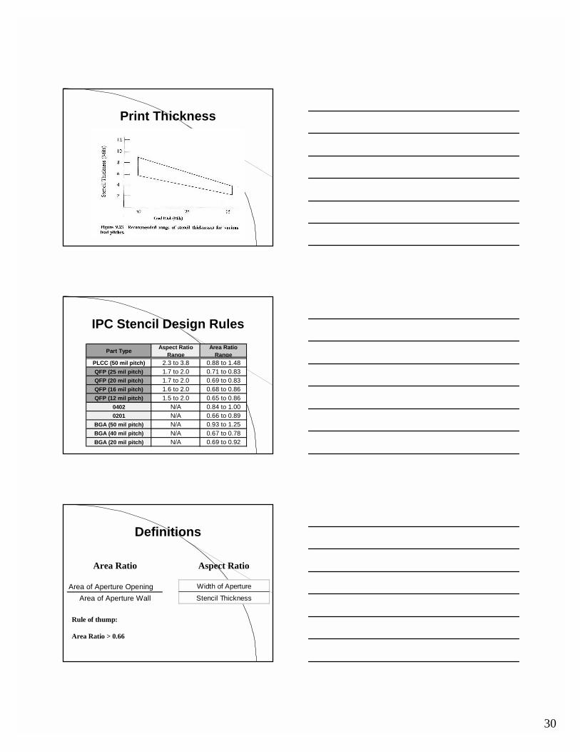
IPC Stencil Design Rules
Part Type Aspect Ratio Range
Area Ratio Range
PLCC (50 mil pitch) 2.3 to 3.8 0.88 to 1.48QFP (25 mil pitch) 1.7 to 2.0 0.71 to 0.83QFP (20 mil pitch) 1.7 to 2.0 0.69 to 0.83QFP (16 mil pitch) 1.6 to 2.0 0.68 to 0.86QFP (12 mil pitch) 1.5 to 2.0 0.65 to 0.86
0402 N/A 0.84 to 1.000201 N/A 0.66 to 0.89
BGA (50 mil pitch) N/A 0.93 to 1.25BGA (40 mil pitch) N/A 0.67 to 0.78BGA (20 mil pitch) N/A 0.69 to 0.92
Definitions
Area of Aperture OpeningArea of Aperture Wall
Area Ratio
Width of ApertureStencil Thickness
Aspect Ratio
Rule of thump:
Area Ratio > 0.66
31
Paste in Hole
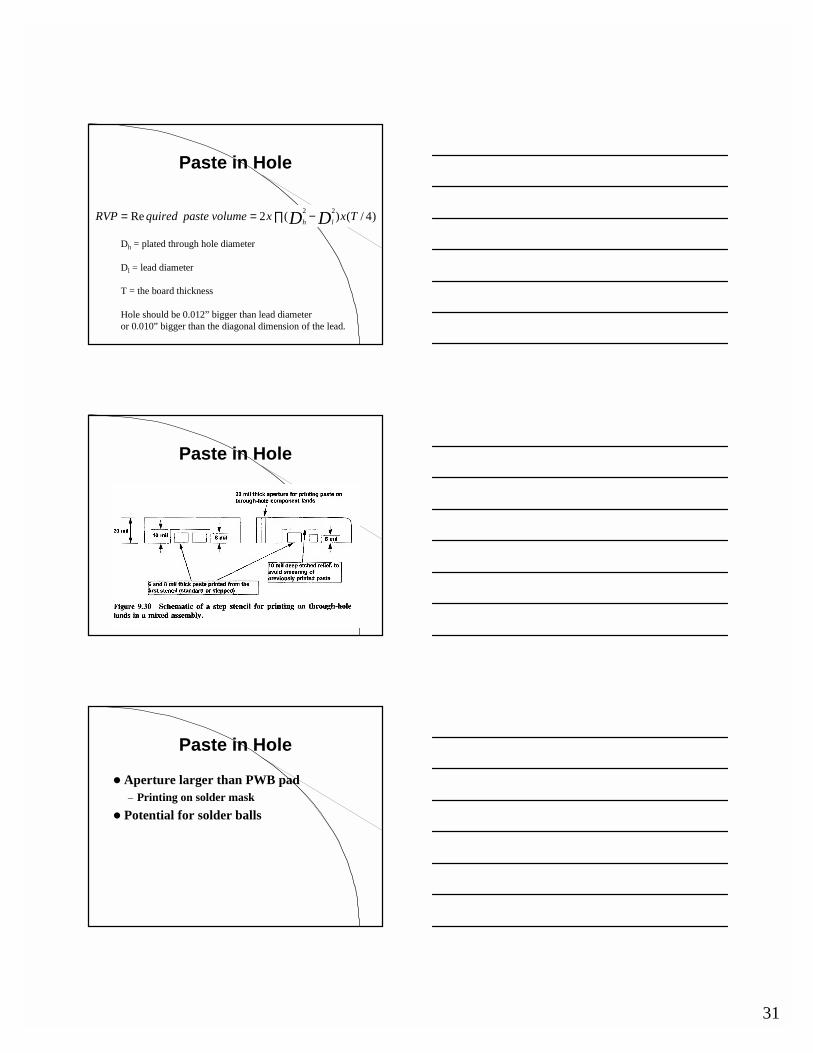
)4/()(2Re 22 TxxvolumepastequiredRVP DD lh −∏==
Dh = plated through hole diameter
Dl = lead diameter
T = the board thickness
Hole should be 0.012” bigger than lead diameteror 0.010” bigger than the diagonal dimension of the lead.
Paste in Hole
Paste in Hole
! Aperture larger than PWB pad– Printing on solder mask
! Potential for solder balls