Embed Size (px)
Citation preview

ELEC 425/ 6261Lecture Notes 2 & 3
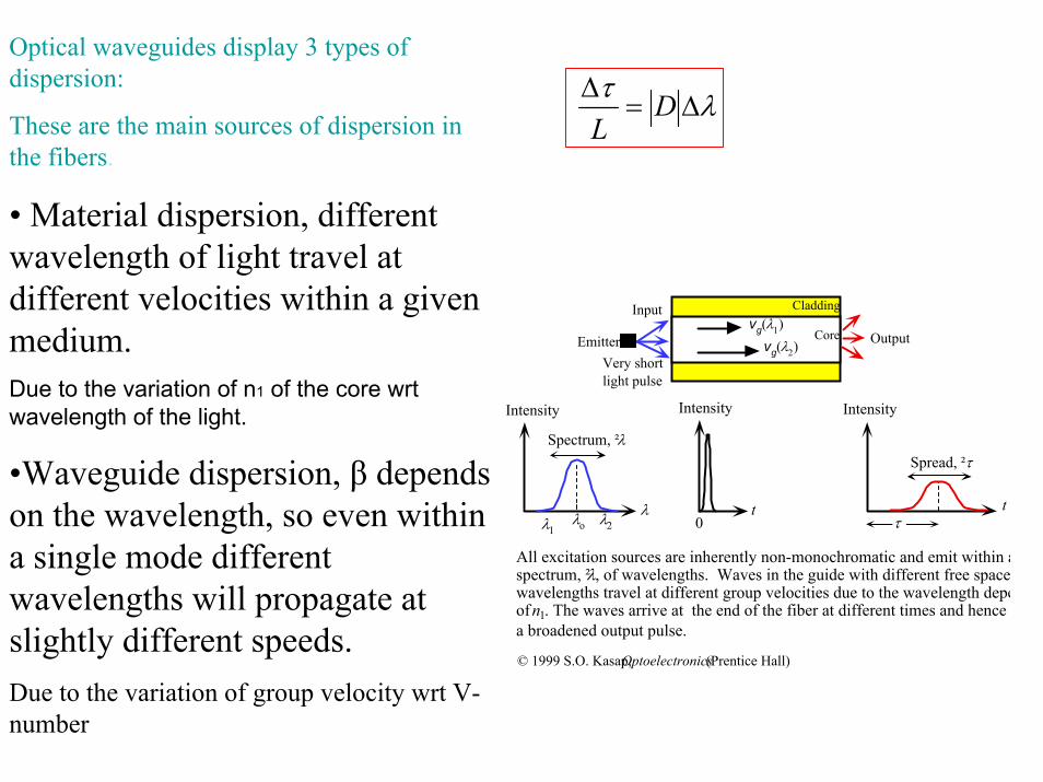
Optical waveguides display 3 types of dispersion:
These are the main sources of dispersion in the fibers.
• Material dispersion, different wavelength of light travel at different velocities within a given medium.Due to the variation of n1 of the core wrtwavelength of the light.
•Waveguide dispersion, β depends on the wavelength, so even within a single mode different wavelengths will propagate at slightly different speeds.Due to the variation of group velocity wrt V-number
τt
Spread, ²τ
t0
λ
Spectrum, ²λ
λ1λ2λo
Intensity Intensity Intensity
Cladding
CoreEmitterVery shortlight pulse
vg(λ2)vg(λ1)
Input
Output
All excitation sources are inherently non-monochromatic and emit within aspectrum, ²λ, of wavelengths. Waves in the guide with different free spacewavelengths travel at different group velocities due to the wavelength depeof n1. The waves arrive at the end of the fiber at different times and hence a broadened output pulse.
© 1999 S.O. Kasap, Optoelectronics (Prentice Hall)
λτΔ=
Δ DL

Optical waveguides display 3 types of dispersion
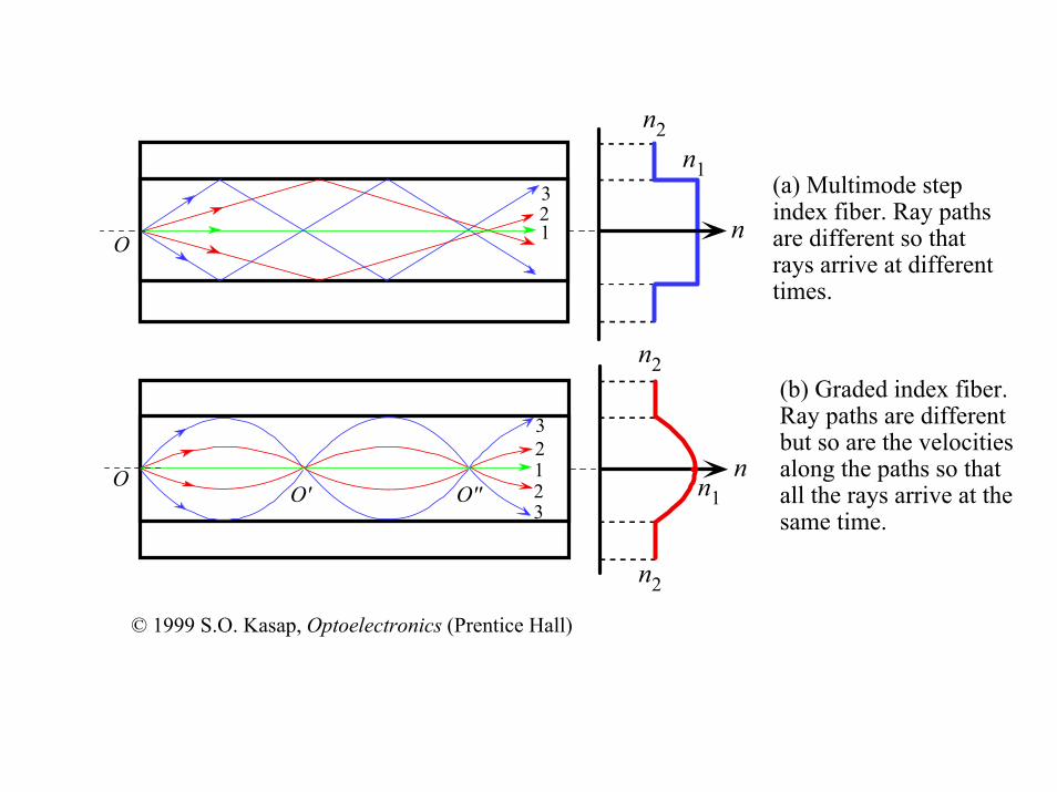
• Modal dispersion, in waveguides with more than one propagating mode. Modes travel with different group velocities.Due to the number of modes traveling along the fiber with different group velocity and different path.
Low order modeHigh order mode
Cladding
Core
Light pulse
t0 t
Spread, Δτ
Broadenedlight pulse
IntensityIntensity
Axial
Schematic illustration of light propagation in a slab dielectric waveguideentering the waveguide breaks up into various modes which then propaggroup velocities down the guide. At the end of the guide, the modes comconstitute the output light pulse which is broader than the input light pul
© 1999 S.O. Kasap, Optoelectronics (Prentice Hall)

0
1.2 1.3 1.4 1.5 1.61.1-30
20
30
10
-20
-10
λ (μm)
Dm
Dm + Dw
Dwλ0
Dispersion coefficient (ps km -1 nm-1)
Material dispersion coefficient (Dm) for the core material (taken asSiO2), waveguide dispersion coefficient (Dw) (a = 4.2 μm) and thetotal or chromatic dispersion coefficient Dch (= Dm + Dw) as afunction of free space wavelength, λ.
© 1999 S.O. Kasap, Optoelectronics (Prentice Hall)
λτΔ=
ΔmD
L
⎟⎟⎠
⎞⎜⎜⎝
⎛−≈ 2
2
λλ
dnd
cDm
λτω Δ=
Δ DL
( ) 22
22
22
984.1
cna
ND g
πω ≈
λτΔ=
ΔPD
Lλτ
ω Δ++=Δ
pm DDDL
Material Dispersion Coefficient
Waveguide Dispersion Coefficient

Core
z
n1x // x
n1y // y
Ey
Ex
Ex
Ey
E
Δτ = Pulse spread
Input light pulse
Output light pulset
t
Δτ
Intensity
Suppose that the core refractive index has different values along two orthogonaldirections corresponding to electric field oscillation direction (polarizations). We cantake x and y axes along these directions. An input light will travel along the fiber with Exand Ey polarizations having different group velocities and hence arrive at the output atdifferent times
© 1999 S.O. Kasap, Optoelectronics (Prentice Hall)
Polarization Dispersion

Material and waveguide dispersion coefficients in anoptical fiber with a core SiO2-13.5%GeO2 for a = 2.5to 4 μm.
0
–10
10
20
1.2 1.3 1.4 1.5 1.6–20
λ (μm)
Dm
Dw
SiO2-13.5%GeO2
2.53.03.54.0a (μm)
Dispersion coefficient (ps km-1 nm-1)
© 1999 S.O. Kasap, Optoelectronics (Prentice Hall)

20
-10
-20
-30
10
1.1 1.2 1.3 1.4 1.5 1.6 1.7
0
30
λ (μm)
Dm
Dw
Dch = Dm + Dw
λ1
Dispersion coefficient (ps km -1 nm-1)
λ2
n
r
Thin layer of claddingwith a depressed index
Dispersion flattened fiber example. The material dispersion coefficient (Dm) for thecore material and waveguide dispersion coefficient (Dw) for the doubly clad fiberresult in a flattened small chromatic dispersion between λ1 and λ2.
© 1999 S.O. Kasap, Optoelectronics (Prentice Hall)

t0
Emitter
Very shortlight pulses
Input Output
Fiber
PhotodetectorDigital signal
Information Information
t0
~2² τ1/2
T
t
Output IntensityInput Intensity² τ1/2
An optical fiber link for transmitting digital information and the effect ofdispersion in the fiber on the output pulses.
© 1999 S.O. Kasap, Optoelectronics (Prentice Hall)
n1
n2
21
3
nO
n1
21
3
n
n2
OO' O''
n2
(a) Multimode stepindex fiber. Ray pathsare different so thatrays arrive at differenttimes.
(b) Graded index fiber.Ray paths are differentbut so are the velocitiesalong the paths so thatall the rays arrive at thesame time.
23
© 1999 S.O. Kasap, Optoelectronics (Prentice Hall)
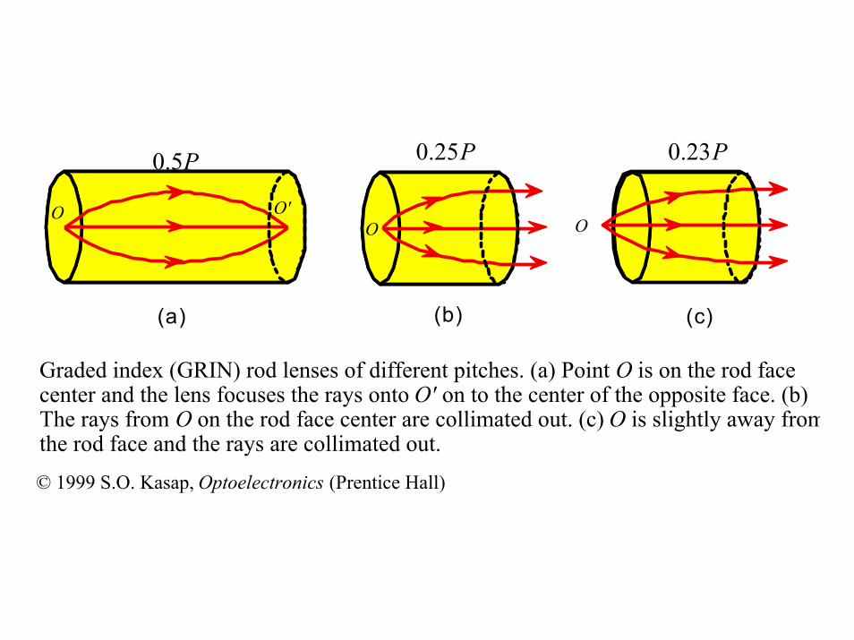
0.5P
O'O
(a)
0.25P
O
(b)
0.23P
O
(c)
Graded index (GRIN) rod lenses of different pitches. (a) Point O is on the rod facecenter and the lens focuses the rays onto O' on to the center of the opposite face. (b)The rays from O on the rod face center are collimated out. (c) O is slightly away fromthe rod face and the rays are collimated out.
© 1999 S.O. Kasap, Optoelectronics (Prentice Hall)

z
A solid with ions
Light directionk
Ex
Lattice absorption through a crystal. The field in the waveoscillates the ions which consequently generate "mechanical"waves in the crystal; energy is thereby transferred from the waveto lattice vibrations.
© 1999 S.O. Kasap, Optoelectronics (Prentice Hall)
Sources of Loss and Attenuation in Fibers

Scattered waves
Incident wave Through wave
A dielectric particle smaller than wavelength
Rayleigh scattering involves the polarization of a small dielectricparticle or a region that is much smaller than the light wavelength.The field forces dipole oscillations in the particle (by polarizing it)which leads to the emission of EM waves in "many" directions sothat a portion of the light energy is directed away from the incidentbeam.© 1999 S.O. Kasap, Optoelectronics (Prentice Hall)

Escaping wave
θ θ
θ′ < θ
θθ > θc θ′
Microbending
R
Cladding
Core
Field distribution
Sharp bends change the local waveguide geometry that can lead to wavesescaping. The zigzagging ray suddenly finds itself with an incidenceangle θ′ that gives rise to either a transmitted wave, or to a greatercladding penetration; the field reaches the outside medium and some lightenergy is lost.
© 1999 S.O. Kasap, Optoelectronics (Prentice Hall)

Attenuation in Optical Fiber
)10(
)log(101
10/Linout
out
indB
PP
PP
Lα
αα
−=
==G. Keiser (Ref. 1)
0.05
0.1
0.51.0
5
10
0.6 0.8 1.0 1.2 1.4 1.6 1.8 2.0
Latticeabsorption
Rayleighscattering
Wavelength (µm)
Illustration of a typical attenuation vs. wavelength characteristicsof a silica based optical fiber. There are two communicationschannels at 1310 nm and 1550 nm.
OH-absorption peaks
1310 nm
1550 nm
© 1999 S.O. Kasap, Optoelectronics (Prentice Hall)

Some Concepts of Solid State MaterialsContents
The Semiconductors in EquilibriumNonequilibrium Condition
Generation-RecombinationGeneration-Recombination rates
Photoluminescence & ElectroluminescencePhoton Absorption
Photon Emission in SemiconductorsBasic Transitions
RadiativeNonradiative
Spontaneous EmissionStimulated Emission
Luminescence EfficiencyInternal Quantum EfficiencyExternal Quantum Efficiency
Photon AbsorptionFresnel Loss
Critical Angle LossEnergy Band Structures of Semiconductors
PN junctionsHomojunctions, Heterojunctions
MaterialsIII-V semiconductors
Ternary SemiconductorsQuaternary SemiconductorsII-VI SemiconductorsIV-VI Semiconductors

The Semiconductors in Equilibrium
• The thermal equilibrium concentration of carriers is independent of time.
• The random generation-recombination of electrons-holes occur continuously due to the thermal excitation.
• In direct band-to-band generation-recombination, the electrons and holes are created-annihilated in pairs:
• Gn0 = Gp0 , Rn0 = Rp0
• -The carriers concentrations are independent of time therefore:
• Gn0 = Gp0 = Rn0 = Rp0

Nonequilibrium Conditions in Semiconductors
• When current exist in a semiconductor device, the semiconductor is operating under nonequilibrium conditions. In these conditions excess electrons in conduction band and excess holes in the valance band exist, due to the external excitation (thermal, electrical, optical…), in addition to thermal equilibrium concentrations.
n(t) = no + δn(t), p(t) = po + δp(t)
• The behavior of the excess carriers in semiconductors (diffusion, drift, recombination, …) which is the fundamental to the operation of semiconductors (electronic, optoelectronic, ..) is described by the ambipolar transport equations.
Generation-Recombination
• In the direct band-to-band the excess electrons and holes are generated and recombined in pair:
g’n0 = g’p0 , R’n0 = R’p0
Generation-Recombination Rates
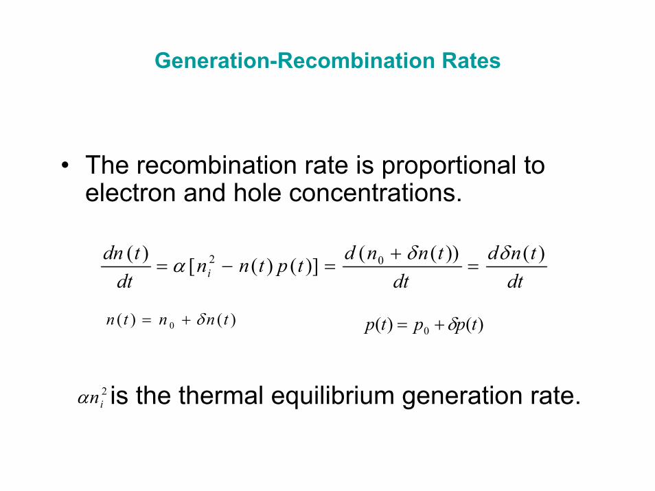
• The recombination rate is proportional to electron and hole concentrations.
is the thermal equilibrium generation rate.
dttnd
dttnndtptnn
dttdn
i)())(()]()([)( 02 δδα =
+=−=
)()( 0 tnntn δ+= )()( 0 tpptp δ+=
2inα

Generation-Recombination Rates
• Electron and holes are created and recombined in pairs, therefore,
• δn(t) = δp(t) and no and po are independent of time.
)]())[(()]())((([))((0000
2 tnpntntpptnnndt
tndi δαδδδαδ
++−=++−=
Considering a p-type material under low-injection condition,
)())((0 tnp
dttnd δαδ
−= 00 )0()0()( n
ttp enentn τα δδδ
−− ==
τno = (αpo)-1 is the minority carrier electrons lifetime, constant for low-injections.

Generation-Recombination Rates
• The recombination rate ( a positive quantity) of excess minority carriers (electrons-holes) for p-type materials is:
0
'' )(
npn
tnRRτ
δ==
Similarly, the recombination rate of excess minority carriers for n-type material is:
0
'' )(p
pntnRR
τδ
==
Generation-Recombination Rates
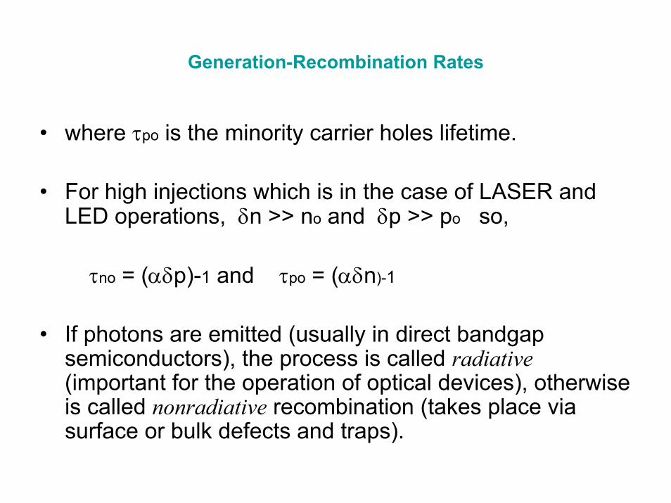
• where τpo is the minority carrier holes lifetime.
• For high injections which is in the case of LASER and LED operations, δn >> no and δp >> po so,
τno = (αδp)-1 and τpo = (αδn)-1
• If photons are emitted (usually in direct bandgapsemiconductors), the process is called radiative(important for the operation of optical devices), otherwise is called nonradiative recombination (takes place via surface or bulk defects and traps).

Generation-Recombination Rates
• In any carrier decay process the total lifetime τ can be expressed as
nrr τττ111
+=
where τr and τnr are the radiative and nonradiative lifetimes respectively.
The total recombination rate is given by
Where Rr and Rnr are radiative and nonradiative recombination rates per unit volume respectively and Rsp is called the spontaneous recombination rate.
spnrrtotal RRRR =+=

Photoluminescence & Electroluminescence
• The recombination of excess carries in direct bandgapsemiconductors may result in the emission of photon. This property is generally referred to as luminescence.
• If the excess electrons and holes are created by photon absorption, then the photon emission from the recombination process is called photoluminescence.
• If the excess carries are generated by an electric current, then the photon emission from the recombination process is called electroluminescence.

Absorption
• When semiconductors are illuminated with light, the photons may be absorbed (for Eph = hν≥Eg= E2 – E1)or they may propagate through the semiconductors (for Eph≤Eg).
• There is a finite probability that electrons in the lower level absorb energy from incoming electromagnetic field (light) with frequency of ν ≥ (E2 – E1)/h and jump to the upper level.
• B12 is proportionality constant, δν = ν2 - ν1 and Φδν = Iνis the photon density in the frequency range of δν.
1121 )( NB
dtdN
ab
δνΦ−=

Absorption
• dN1 states are raised from E1 to E2 i.e dN1 photons are absorbed.• Electrons are created in conduction band and holes in valence
band. • When photons with an intensity of Iν (x) are traveling through a
semiconductor, going from x position to x + dx position (in 1-D system), the energy absorbed by semiconductor per unit of time is given by αIν (x)dx, where α is the absorption coefficient; the relative number of photons absorbed per unit distance (cm-1).
dxxIdxdx
xdIxIdxxI )(.)()()( νν
νν α−==−+
)()(
xIdx
xdIν
ν α−=
xeIxI ανν
−= 0)( where Iν(0) = Iν0 .

Absorption
• Intensity of the photon flux decreases exponentially with distance.• The absorption coefficient in semiconductor is strong function of
photon energy and band gap energy.• The absorption coefficient for hν < Eg is very small, so the
semiconductor appears transparent to photons in this energy range.

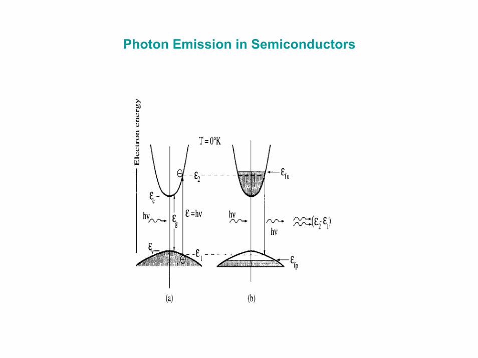
Photon Emission in Semiconductors
• When electrons in semiconductors fall from the conduction band to the valence band, called recombination process, release their energy in form of light (photon), and/or heat (lattice vibration, phonon).
• N1 and N2 are the concentrations of occupied states in level 1 (E1) and level 2 (E2) respectively.
Basic Transitions
RadiativeIntrinsic emissionEnergetic carriers
NonradiativeImpurities and defect center involvement
Auger process

Photon Emission in Semiconductors

Photon Emission in Semiconductors

Photon Emission in Semiconductors

Photon Emission in Semiconductors

Photon Emission in Semiconductors
Photon Emission in Semiconductors


Einstein Relationship

Einstein Relationship


Wave attenuation


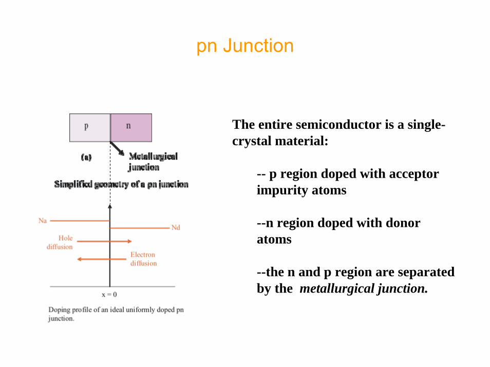
pn Junction
The entire semiconductor is a single-crystal material:
-- p region doped with acceptor impurity atoms
--n region doped with donor atoms
--the n and p region are separated by the metallurgical junction.
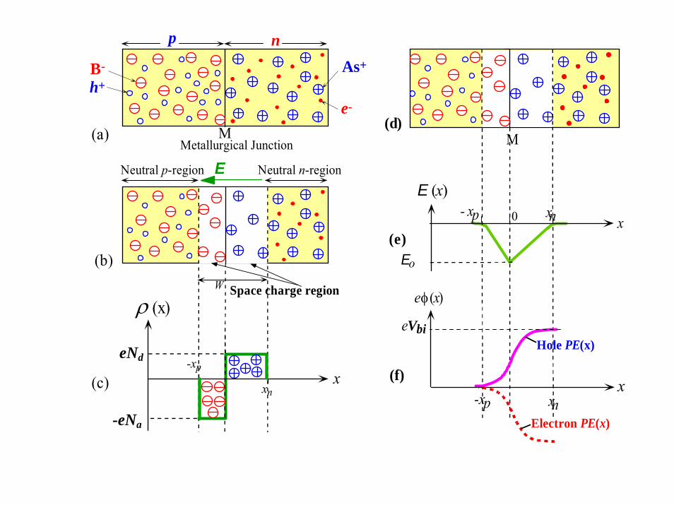
-eNa
eNd
x
B-
h+
p n
M
As+
e-
W
Neutral n-regionNeutral p-region
Space charge region
Metallurgical Junction(a)
(b)
-xp
xn(c)
E E (x)
eVbi
e φ (x)
x
x0
Eo
M
xn
xn
- xp
- xp
(e)
(f)
(d)
ρ (x)
Hole PE(x)
Electron PE(x)

- the potential barrier :
- keeps the large concentration of electrons from flowing from the n region into the p region;
- keeps the large concentration of holes from flowing from the p region into the n region;
=> The potential barrier maintains thermal equilibrium.

- the potential of the n region is positive with respect to the p region => the Fermi energy in the n region – lower than the Fermi energy in the p region;
- the total potential barrier – larger than in the zero-bias case;
- still essentially no charge flow and hence essentially no current;

-a positive voltage is applied to the p region with respect to the n region;
- the Fermi energy level – lower in the p region than in the n region;
- the total potential barrier – reduced => the electric field in the depletion region – reduced;
⇒ diffusion of holes from the p region across the depletion region into the n region;
⇒ diffusion of electrons from the n region across the depletion region into the p region;
- diffusion of carriers => diffusion currents;

⎟⎟⎠
⎞⎜⎜⎝
⎛= 2ln
i
datbi n
NNVV
-in thermal equilibrium :
- the n region contains many more electrons in the conduction band than the p region;
- the built-in potential barrier prevents the large density of electrons from flowing into the p region;
- the built-in potential barrier maintains equilibrium between the carrier distribution on either side of the junction;
⎟⎠⎞
⎜⎝⎛ −
=kTqVnn bi
np exp00

- the electric field Eapp induced by Va – in opposite direction to the electric field in depletion region for the thermal equilibrium;
- the net electric field in the depletion region is reduced below the equilibrium value;
- majority carrier electrons from the n side -> injected across the depletion region into the p region;
- majority carrier holes from the p region -> injected across the depletion region into the n region;
- Va applied => injection of carriers across the depletion regions-> a current is created in the pn junction;


2/1
max
2/1
max
2/1
2
)(2)(2
)(2
⎪⎭
⎪⎬⎫
⎪⎩
⎪⎨⎧
⎥⎦
⎤⎢⎣
⎡+
−≅
>>
+−=
⎪⎭
⎪⎬⎫
⎪⎩
⎪⎨⎧
⎥⎦
⎤⎢⎣
⎡+
+−=
⎪⎭
⎪⎬⎫
⎪⎩
⎪⎨⎧
⎥⎦
⎤⎢⎣
⎡ ++=+=
da
da
s
R
biR
Rbi
da
da
s
Rbi
da
daRbispn
NNNNeVE
VV
WVV
NNNNVVeE
NNNN
eVVxxW
ε
ε
ε
212
⎪⎭
⎪⎬⎫
⎪⎩
⎪⎨⎧
⎟⎟⎠
⎞⎜⎜⎝
⎛ +=+=
da
dabisnp NN
NNeVxxW ε For zero bias
For reverse biased
WVE bi2
max−
=
For reverse biased
For zero bias

When there is no voltage applied across the pn junction the junction is in thermal equilibrium => the Fermi energy level –constant throughout the entire system.
FpFnbiV Φ+Φ=
⎟⎟⎠
⎞⎜⎜⎝
⎛=⎟⎟
⎠
⎞⎜⎜⎝
⎛=⎟⎟
⎠
⎞⎜⎜⎝
⎛=
p
n
n
p
i
dabi n
ne
kTpp
ekT
nNN
ekTV lnln 2
⎟⎟⎠
⎞⎜⎜⎝
⎛+⎟⎟
⎠
⎞⎜⎜⎝
⎛=−+−=Φ+Φ=
i
d
i
aFiFnFpFinpbi n
Ne
kTnN
ekTeEEeEEV lnln/)(/)(

dxxdEx
dxxd
EquationsPoisson
s
)()()(
'
2
2−=
−=
ερφ
+
_
ρ(C/cm³)deN+
aeN−
nx+px−
E
x =0
∫−=x
xs pdxxxE )(1)( ρ
ε
nns
d
pps
a
xxxxeNE
xxxxeNE
≤≤−−
=
≤≤−+−
=
0),(
0),(
ε
ε
cmFSiFor rs /)1085.8)(7.11( 140
−×=⋅= εεε
ndpa xNxN =
Charge neutrality:
The peak electric field Is at x = 0
s
pa
s
nd xeNxeNEεε
−=−=max
nx+px−
Emax

⎥⎥⎦
⎤
⎢⎢⎣
⎡+=
n
pn
p
nps L
nqDL
pqDJ 00
⎥⎦
⎤⎢⎣
⎡−⎟
⎠⎞
⎜⎝⎛= 1exp
kTqVJJ a
s - ideal-diode equation;

The bipolar transistor:
- tree separately doped regions
- two pn junctions;
The width of the base region – small compared to the minority carrier diffusion length;
The emitter – largest doping concentration;
The collector – smallest doping concentration;

- the bipolar semiconductor – not a symmetrical device;
-the transistor – may contain two n regions or two p regions -> the impurity doping concentrations in the emitter and collector = different;
-- the geometry of the two regions –can be vastly different;


Electromagnetic Spectrum
• Three basic bands; infrared (wavelengths above 0.7μm), visible (wavelengths between 0.4-0.7μm), and ultraviolet light (wavelengths below 0.4μm).
• E = hν = hc/ λ ; c = νλ
• An emitted light from a semiconductor optical device has a wavelength proportional to the semiconductor band-gap.
• Longer wavelengths for communication systems; Eg ≈ 1μm. (lower Fiber loss).
• Shorter wavelengths for printers, image processing,… Eg > 1μm.
• Semiconductor materials used to fabricate optical devices dependon the wavelengths required for the operating systems.

Materials
• Almost all optoelectronic light source depend upon epitaxial crystal growth techniques where a thin film (a few microns) of semiconductor alloys are grown on single-crystal substrate; the film should have roughly the same crystalline quality. It is necessary to make strain-free heterojunction with good-quality substrate. The requirement of minimizing strain effectsarises from a desire to avoid interface states and to encourage long-term device reliability, and this imposes a lattice-matching condition on the materials used.
Materials
• The constraints of bandgap and lattice match force that more complex compound must be chosen. These compounds include ternary (compounds that containing three elements) and quaternary (consisting of four elements) semiconductors of the form AxB1-xCyD1-y; variation of x and y are required by the need to adjust the band-gap energy (or desired wavelength) and for better lattice matching. Quaternary crystals have more flexibility in that the band gap can be widely varied while simultaneously keeping the lattice completely matched to a binary crystal substrate. The important substrates that are available for the laser diode technology are GaAs, InP and GaP. A few semiconductors and their alloys can match with these substrates. GaAs was the first material to emit laser radiation,and its related to III-V compound alloys, are the most extensively studied developed.

Materials
• III-V semiconductors• Ternary Semiconductors; Mixture of binary-binary
semiconductors; AxB1-xC; mole fraction, x, changes from 0 to 1.(x will be adjusted for specific required wavelength).
• GaxAl1-xAs ; In0.53Ga0.47As; In0.52Al0.48As
- Vegard’s Law: The lattice constant of AxB1-xC varies linearly from the lattice constant of the semiconductor AC to that of the semiconductor BC.
- The bandgap energy changes as a quadratic function of x.
- The index of refraction changes as x changes.• The above parameters cannot vary independently
(due to the only one degree of freedom).
• Quaternary Semiconductors; AxB1-xCyD1-y • (x and y will be adjusted for specific wavelength and
matching lattices).
• GaxIn1-xPyAs1-y ; (AlxGa1-x)yIn1-yP; AlxGa1-xAsySb1-y
2cxbxaEg ++=
Materials
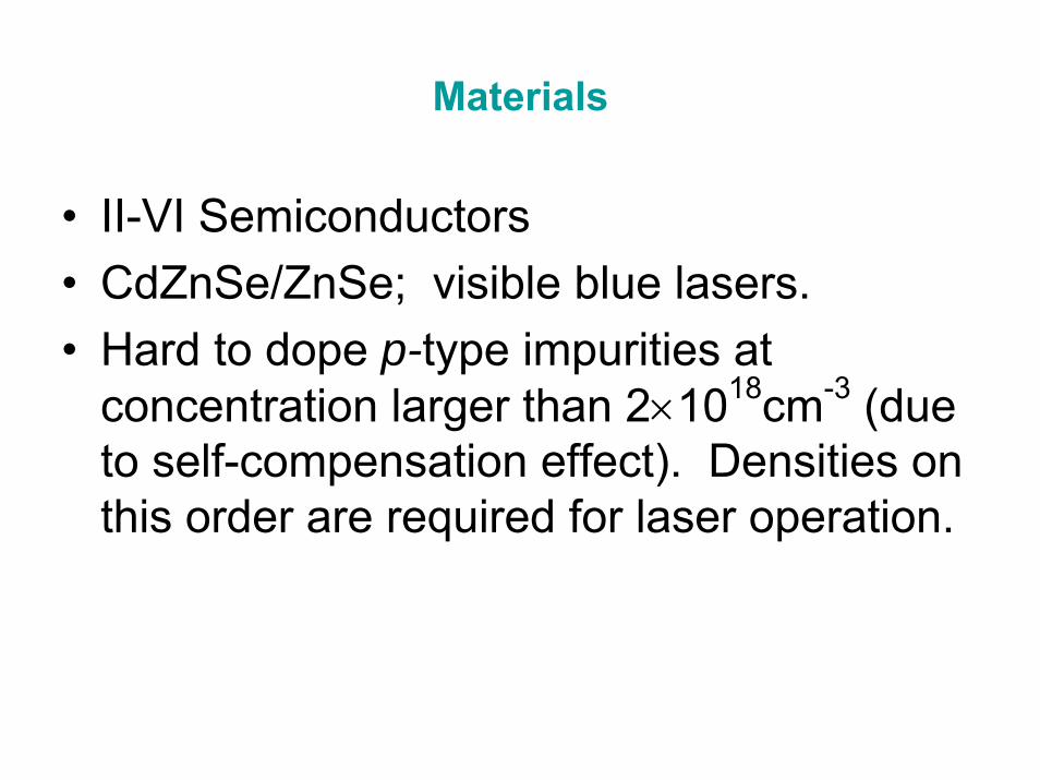
• II-VI Semiconductors• CdZnSe/ZnSe; visible blue lasers.• Hard to dope p-type impurities at
concentration larger than 2×1018cm-3 (due to self-compensation effect). Densities on this order are required for laser operation.

Materials
• IV-VI semiconductors• PbSe; PbS; PbTe• By changing the proportion of Pb atoms in
these materials semiconductor changes from n- to p-type.
• Operate around 50 Ko
• PbTe/Pb1-xEuxSeyTe1-y operates at 174 Ko

Materials

Materials

Materials

Materials
• In the near infrared region, the most important and certainly the most extensively characterized semiconductors are GaAs, AlAs and their ternary derivatives AlxGa1-xAs.
• At longer wavelengths, the materials of importance are InP and ternary and quaternary semiconductors lattice matched to InP. The smaller band-gap materials are useful for application in the long wavelength range. The III-V compounds of interest here are antimony (Sb)-bearing compounds and InAs and their ternary and quaternary.


Energy Band Structure of Semiconductors

Basic Semiconductor Luminescent Diode StructuresLEDs (Light Emitting Diode)
• Under forward biased when excess minority carriers diffuse into the neutral semiconductor regions where they recombine with majority carriers. If this recombination process is direct band-to-band process, photons are emitted. The output photon intensity will be proportional to the ideal diode diffusion current.
• In GaAs, electroluminescence originated primarily on the p-side of the junction because the efficiency for electron injection is higher than that for hole injection.
• The recombination is spontaneous and the spectral outputs have a relatively wide wavelength bandwidth of between 30 – 40 nm.
• λ = hc/Eg = 1.24/ Eg

Basic Semiconductor Luminescent Diode Structures

Basic Semiconductor Luminescent Diode Structures

hυ - Eg
Eg (b)
V
(a)
p n+
Eg
eVo
EF
p n+
Electron in CBHole in VB
Ec
Ev
Ec
Ev
EF
eVo
Electron energy
Distance into device
(a) The energy band diagram of a p-n+ (heavily n-type doped) junction without any bias.Built-in potential Vo prevents electrons from diffusing from n+ to p side. (b) The appliedbias reduces Vo and thereby allows electrons to diffuse, be injected, into the p-side.Recombination around the junction and within the diffusion length of the electrons in thep-side leads to photon emission.
© 1999 S.O. Kasap, Optoelectronics (Prentice Hall)

Light output
Insulator (oxide)p
n+ Epitaxial layer
A schematic illustration of typical planar surface emitting LED devices. (a) p-layergrown epitaxially on an n+ substrate. (b) First n+ is epitaxially grown and then p regionis formed by dopant diffusion into the epitaxial layer.
Light output
pEpitaxial layers
(a ) (b )
n+Substrate Substrate
n+
n+
Metal electrode
© 1999 S.O. Kasap, Optoelectronics (Prentice Hall)

Light output
p
Electrodes
LightPlastic dome
Electrodes
Domedsemiconductor
pn Junction
(a) (b) (c)
n+n+
(a) Some light suffers total internal reflection and cannot escape. (b) Internal reflectionscan be reduced and hence more light can be collected by shaping the semiconductor into adome so that the angles of incidence at the semiconductor-air surface are smaller than thecritical angle. (b) An economic method of allowing more light to escape from the LED isto encapsulate it in a transparent plastic dome.
Substrate
© 1999 S.O. Kasap, Optoelectronics (Prentice Hall)

Ec
Ev
EN
(b) N doped GaP
Eg
(a) GaAs1-yPy
y < 0.45(a) Photon emission in a direct bandgap semiconductor. (b). GaP is anindirect bandgap semiconductor. When doped with nitrogen there is anelectron trap at EN. Direct recombination between a trapped electron at ENand a hole emits a photon. (c) In Al doped SiC, EHP recombination isthrough an acceptor level like Ea.
Ec
Ev
Ea
(c) Al doped SiC
© 1999 S.O. Kasap, Optoelectronics (Prentice Hall)

0.4 0.5 0.6 0.7 0.8 0.9 1.0 1.1 1.2 1.3 1.4 1.5 1.6λ
1.7Infrared
GaAs1-yPy
In1-xGaxAs1-yPyAlxGa1-xAs
x = 0.43
Indirectbandgap
Free space wavelength coverage by different LED materials from the visible spectrum to theinfrared including wavelengths used in optical communications. Hatched region and dashedlines are indirect Eg materials.
In0.49AlxGa0.51-xP
© 1999 S.O. Kasap, Optoelectronics (Prentice Hall)

2 eV
2 eVeVo
Holes in VB
Electrons in CB1.4 eV
No bias
Withforwardbias
Ec
EvEc
Ev
EFEF
(a)
(b)
(c)
(d)
pn+ p
ΔEc
GaAs AlGaAsAlGaAs
ppn+
~ 0.2 μm
AlGaAsAlGaAs
(a) A doubleheterostructure diode hastwo junctions which arebetween two differentbandgap semiconductors(GaAs and AlGaAs)
(b) A simplified energyband diagram withexaggerated features. EFmust be uniform.
(c) Forward biasedsimplified energy banddiagram.
(d) Forward biased LED.Schematic illustration ofphotons escapingreabsorption in theAlGaAs layer and beingemitted from the device.
© 1999 S.O. Kasap, Optoelectronics (Prentice Hall)
GaAs

E
Ec
Ev
Carrier concentrationper unit energy
Electrons in CB
Holes in VBhυ
1
0
Eg
hυ1
hυ2
hυ3
CB
VBλ
Relative intensity
1
0λ
1λ
2λ
3
ΔλΔhυ
Relative intensity
(a) (b) (c) (d)
Eg + kBT
(2.5-3)kBT
1/2kBT
Eg1 2 3
2kBT
(a) Energy band diagram with possible recombination paths. (b) Energy distribution ofelectrons in the CB and holes in the VB. The highest electron concentration is (1/2)kBT aboveEc . (c) The relative light intensity as a function of photon energy based on (b). (d) Relativeintensity as a function of wavelength in the output spectrum based on (b) and (c).
© 1999 S.O. Kasap, Optoelectronics (Prentice Hall)

V
2
1
(c)
0 20 40I (mA)0
(a)
600 650 7000
0.5
1.0
λ
Relativeintensity
24 nm
Δλ
655nm
(b)
0 20 40I (mA)0
Relative light intensity
(a) A typical output spectrum (relative intensity vs wavelength) from a red GaAsP LED.(b) Typical output light power vs. forward current. (c) Typical I-V characteristics of ared LED. The turn-on voltage is around 1.5V.© 1999 S.O. Kasap, Optoelectronics (Prentice Hall)

(a) Surface emitting LED (b) Edge emitting LED
Doubleheterostructure
Light
Light
© 1999 S.O. Kasap, Optoelectronics (Prentice Hall)

ElectrodeSiO2 (insulator)
Electrode
Fiber (multimode)
Epoxy resin
Etched wellDouble heterostructure
Light is coupled from a surface emitting LEDinto a multimode fiber using an index matchingepoxy. The fiber is bonded to the LEDstructure.
(a)
Fiber
A microlens focuses diverging light from a surfaceemitting LED into a multimode optical fiber.
Microlens (Ti2O3:SiO2 glass)
(b)
© 1999 S.O. Kasap, Optoelectronics (Prentice Hall)

Schematic illustration of the the structure of a double heterojunction stripecontact edge emitting LED
InsulationStripe electrode
SubstrateElectrode
Active region (emission region)
p+-InP (Eg = 1.35 eV, Cladding layer)
n+-InP (Eg = 1.35 eV, Cladding/Substrate)
n-InGaAs (Eg = 0.83 eV, Active layer)
Currentpaths
L
60-70 μm
Light beam
p+-InGaAsP (Eg = 1 eV, Confining layer)
n+-InGaAsP (Eg = 1 eV, Confining layer) 12 3200-300 μm
© 1999 S.O. Kasap, Optoelectronics (Prentice Hall)

Multimode fiberLens
(a)
ELED
Active layer
Light from an edge emitting LED is coupled into a fiber typically by using a lens or aGRIN rod lens.
GRIN-rod lens
(b)
Single mode fiberELED
© 1999 S.O. Kasap, Optoelectronics (Prentice Hall)

L λλmλm - 1
Fabry-Perot etalon
Partially reflecting plates
Output lightInput light
Transmitted light
Transmitted light through a Fabry-Perot optical cavity.
© 1999 S.O. Kasap, Optoelectronics (Prentice Hall)
( )20
max 1 RI
I−
=( )
( ) ( )kLRRRII incidentdtransmitte 22
2
sin411+−−
=

A
BL
M1 M2 m = 1
m = 2
m = 8
Relative intensity
υ
δυm
υm υm + 1υm - 1
(a) (b) (c)
R ~ 0.4R ~ 0.81 υf
Schematic illustration of the Fabry-Perot optical cavity and its properties. (a) Reflectedwaves interfere. (b) Only standing EM waves, modes, of certain wavelengths are allowedin the cavity. (c) Intensity vs. frequency for various modes. R is mirror reflectance andlower R means higher loss from the cavity.
© 1999 S.O. Kasap, Optoelectronics (Prentice Hall)
Lm =⎟⎠⎞
⎜⎝⎛
2λ m=1,2,3….
( ) ( )KLRRI
Icavity 220
sin41 +−=

LASERS
• The sensitivity of most photosensitive material is greatly increased at wave-length < 0.7 μm; thus, a laser with a short wave-length is desired for such applications as printers and image processing. The sensitivity of the human eye range between the wavelengths of 0.4 and 0.8μm and the highest sensitivity occur at 0.555μm or green so it is important to develop laser in this spectral regime for visual applications.
• Laser-quality crystals are obtained only with lattice mismatches <0.01% relative to the substrate. It is generally true that semiconductor materials with larger band gaps show a tendency to have small lattice constants.

LASERS
• The semiconductor laser diode is a forward bias p-n junction. The structure appears to be similar to the LED as far as the electron and holes are concerned, but it is quite different from the point of view of the photons. Electrons and holes are injected into an active region by forward biasing the laser diode. At low injection, these electrons and holes recombine (radiative) via the spontaneous process to emit photons. However, the laser structure is so designed that at higher injections the emission process occurs by stimulated emission. As we will discuss, the stimulated emission process provides spectral purity to the photon output, provides coherent photons, and offers high-speed performance.
• The exact output spectrum from the laser diode depends both on the nature of the optical cavity and the optical gain versus wavelength characteristics.
•• Lasing radiation is only obtained when optical gain in the medium can
overcome the photon loss from the cavity, which requires the diode current I to exceed a threshold value Ith and gop>gth

LASER Diode Modes of Threshold Conditions
Lasing Conditions:Population Inversion
Fabry-Perot cavity
gain (of one or several modes) > optical loss
( ) zhvhvg
eIzI ⎥⎥⎥
⎦
⎤
⎢⎢⎢
⎣
⎡−Γ
−
=α)(
)0()(
I – optical field intensityg – gain coefficient in F.P. cavity
- effective absorption coefficientΓ – optical field confinement factor. (the fraction of optical power in the active layer)
−
α
In one round trip i.e. z = 2L gain should be > loss for lasing;During this round trip only R1 & R2 fractions of optical radiation are reflected from the two laser ends 1 & 2.
2
21
21⎟⎟⎠
⎞⎜⎜⎝
⎛+−
=nnnn
R

LASER Diode Modes of Threshold Conditions
From the laser conditions: )()2( oILI = 12 =− Lje β ( )mL πβ 22 =
)0()0()2(_
2
21 IeRRILIgL
==⎥⎦
⎤⎢⎣
⎡−Γ α
21
2 1_
RRe
gL
=⎥⎦
⎤⎢⎣
⎡−Γ α
21
_ 1ln2RR
gL =⎟⎠⎞
⎜⎝⎛ −Γ α
endth RRLg ααα +=+=Γ
_
21
_ 1ln21
Lasing threshold is the point at which the optical gain is equal to the total loss αt
endtthg ααα +==Γ_
thth Jgg β=≥
β – is constant and depends on the specific device construction.
Thus the gain

Laser Diode Rate Equations
Rate Equations govern the interaction of photons and electrons in the active region.
phspRBn
dtd
τφφφ
−+= = stimulated emission + spontaneous emission - photon loss
φτ
BnnqdJ
dtdn
sp
−−= = injection - spontaneous recombination - stimulated emission
(shows variation of electron concentration n).
Variation of photon concentration:
The relationship between optical output and the diode drive current:
d - is the depth of carrier-confinement regionB - is a coefficient (Einstein’s) describing the strength of the optical absorption and emission interactions,;Rsp - is rate of spontaneous emission into the lasing mode; τph – is the photon lifetime;τsp – is the spontaneous recombination lifetime; J – is the injection current density;

Laser Diode Rate Equations
Solving the above Equations for a steady-state condition yields an expression for the output power.
0=dtd φ 0=
dtdnSteady-state => and
0>dtd φ 01
≥−ph
BnτIf we neglect Rsp and noting =>
Therefore, n must exceed a threshold value nth in order for Φ to increase. In other words J needs to exceed Jth in steady-state condition, when the number of photons Φ=0.
sp
thth nqdJ
τ=

Laser Diode Rate Equations
⎪⎪⎩
⎪⎪⎨
⎧
=+−Φ−
=Φ
−+Φ
0
0
qdJn
BN
RBN
sp
thsth
ph
sspsth
τ
τ
This expression defines the current required to sustain an excess electron density in the laser when spontaneous emission is the only decay mechanism.
Now, under steady-state condition at the lasing threshold:
Фs is the steady-state photon density.
0=+−Φ
−qdJnR
sp
th
ph
ssp ττ
phphsp
thphsps qd
JnR τττ
τ +−=Φ
qdJn
sp
th =τ
( ) phspthph
s RJJqd
ττ
+−=Φ
# of photon resulting from stimulated emission
Adding these two equations: but
The power from the first term is generally concentrated in one or few modes;The second term generates many modes, in order of 108 modes.

Laser Diode Rate Equations
To find the optical power P0:
cnLt =Δ time for photons to cross cavity length L.
sΦ21 - is the part travels to right or left (toward output
face)
R is part of the photons reflected and 1-R part will escape the facet
( )( )( )
t
RhvvolumeP
s
Δ
−⎟⎠⎞
⎜⎝⎛ Φ
=1
21
0
[ ]thph JJ
qnRWhc
P −⎥⎥⎦
⎤
⎢⎢⎣
⎡ −=
λτ
2)1(2
0
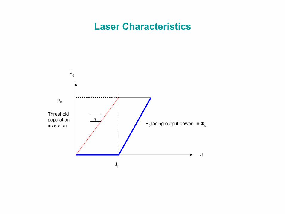
Laser Characteristics
P0
J
Jth
nth
P0 lasing output power ≡ Фs
Thresholdpopulationinversion
n
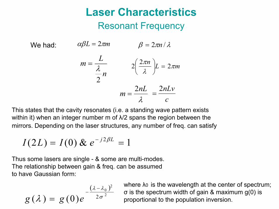
Laser CharacteristicsResonant Frequency
mL παβ 2= λπβ /2 n=
mLn πλπ 222 =⎟
⎠⎞
⎜⎝⎛
cnLv2
=λnLm 2
=
We had:
n
Lm
2λ
=
This states that the cavity resonates (i.e. a standing wave pattern exists within it) when an integer number m of λ/2 spans the region between the mirrors. Depending on the laser structures, any number of freq. can satisfy
1&)0()2( 2 == − LjeILI β
Thus some lasers are single - & some are multi-modes. The relationship between gain & freq. can be assumed to have Gaussian form:
( )2
20
2)0()( σλλ
λ−
−= egg
where λ0 is the wavelength at the center of spectrum; σ is the spectrum width of gain & maximum g(0) is proportional to the population inversion.

Laser CharacteristicsSpacing between the modes:
mvcLnm 2
= Ln
m=
2λ
121 −=− mv
cLnm
nLmnL
mnL
mnL
m 22
122 2
2
λδλ ==+
−=
( ) 1221 =Δ=− − v
cLnvv
cLn
mm Lncv
2=Δ
λvc =2λλΔ
−=Δ=>=cv
vcv
LnLncc
22
2
2
λλλ
λ=Δ=>=
Δ

Laser CharacteristicsInternal & External Quantum Efficiency
Quantum Efficiency (QE) = # of photons generated for each EHP injected into the semiconductor junction ≡ a measure of the efficiency of the electron-to-photon conversion process.If photons are counted at the junction region, QE is called internal QE (ηint), which depends on the materials of the active junction and the neighboring regions. For GaAs ηint = 65% to 100%.If photons are counted outside the semiconductor diode QE is external QE(ηext).
Consider an optical cavity of length L , thickness W and width S. Defining a threshold gain gth as the optical gain needed to balance the total power loss, due to various losses in the cavity, and the power transmission through the mirrors .

Laser CharacteristicsInternal & External Quantum Efficiency
The optical intensity due to the gain is equal to:I = Io exp(2Lgth), this will be lost due to the absorption and the reflections on both ends by
R1R2 exp(-2Lα)
So: I = Io exp(2Lgth){ R1R2 exp(-2Lα)} = Io . Therefore:
1)(221 =−αthgLeRR
where R1 and R2 are power reflection coefficients of the mirrors, α is attenuation constant.

Laser CharacteristicsInternal & External Quantum Efficiency
21
1ln21
RRLgth += α
g is gain constant of the active region and is roughly proportional to current density (g = βJ). β is a constant.
( )21
1ln21)/1(
RRLJth += αβ By measuring Jth, α, L, Γ1 and Γ2 one
can calculate β (dependent upon the materials and the junction structure).
The ratio of the power radiated through mirrors to the total power generated by the semiconductor junction istotal
ra
PP
RRL
RRL≡
+21
21
1ln21
1ln21
α
Laser CharacteristicsInternal & External Quantum Efficiency
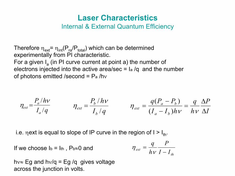
Therefore ηext= ηint(Pra/Ptotal) which can be determined experimentally from PI characteristic.For a given Ia (in PI curve current at point a) the number of electrons injected into the active area/sec = Ia /q and the number of photons emitted /second = Pa /hν
qIhP
a
aext /
/ νη =
qIhP
b
bext /
/ νη =
IP
hq
hIIPPq
ba
baext Δ
Δ=
−−
=νν
η)(
)(
i.e. ηext is equal to slope of IP curve in the region of I > Ith.
thext II
Phq
−=
νηIf we choose Ib = Ith , Pb≈0 and
hν≈ Eg and hν/q = Eg /q gives voltage across the junction in volts.

Laser CharacteristicsPower Efficiency
At dc or low frequency the equivalent circuit to a LASER diode may be viewed as an ideal diode in series with rs.
Therefore the power efficiency = ηp =(optical power output)/ (dc electrical power input)
sgp rIqEI
P2)/( +
=η
extthIIq
hP ην )( −=
sg
gthextp rIqEI
qEII2)/(/)(
+
−=
ηη