Embed Size (px)
Citation preview
Koc University Elec 204: Digital System Design Laboratory Experiment 5
ELEC 204 Digital System Design
LABORATORY MANUAL
Experiment 5: Design and Implementation of a 3-bit Up/Down Johnson
Counter
College of Engineering Koç University
Important Note: In order to effectively utilize the laboratory sessions, you should read the manual and prepare the experiments before the sessions.
Koc University Elec 204: Digital System Design Laboratory Experiment 5
1. Objectives:
The purpose of this lab is:
1. To get familiar with the flip-flops 2. To design an up/down Johnson counter using D flip-flops 3. To implement the counter using Xilinx FPGA board 4. To experimentally check the operation of the counter
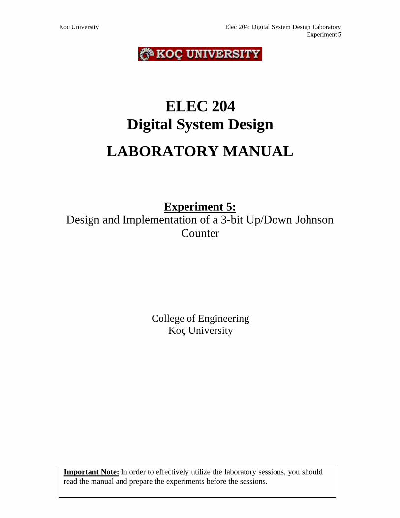
The goal is to design a Johnson counter that can count up or down, depending on the setting of a control input UP/DOWN. The counter has an asynchronous reset (or clear) input which brings the outputs to 0 as soon as the RESET signal is asserted. The counter counts at the negative edge of the clock. When the UP input is high, the counter counts in one direction and when UP is low, it counts in the other direction, as shown in the state transition diagram.
Figure 1: State transition diagram for up/down counter.
2. Equipments:
• Spartan Board • Pentium PC • Cables/wires to connect them • Adapter to supply power to Spartan board
Koc University Elec 204: Digital System Design Laboratory Experiment 5
2. Preliminary Work
1. Review the design procedure in your class notes or the textbook for counters.
2. Use the standard counter design process to design this up/down counter with D flip-flops. Notice that the asynchronous reset will bring the counter in a known and allowed state (000).
a. Give the state transition table (consider the UP signal as an input together with the three present states).
b. Draw the K-maps for the three D inputs: DA, DB and DC.
c. Give the logic expression and logic diagram of each function DA, DB and DC. Can you see similarities between these three functions?
d. This state machine will have unused states. In case you get stuck into one of these unused states, e.g. state (010), what will the next two states be, assuming that you do not use the reset switch to get back into the starting state: (010) -> (???) -> (???). Is this a self-starting counter?
e. Based on the similarities (or symmetries) of the three functions DA, DB and DC, can you extend the design to more bits? Give the expressions of DA, DB, DC, and DD for a 4-bit Johnson counter. Also draw the schematic in your notebook.
3. Sketch the full diagram of the 4-bit Johnson counter (logic and FF) using negative edge triggered D flip-flops with an asynchronous reset. Assume that the D flip-flops are available as building blocks (you do not have to design your own flip-flop).
3 Experimental Work
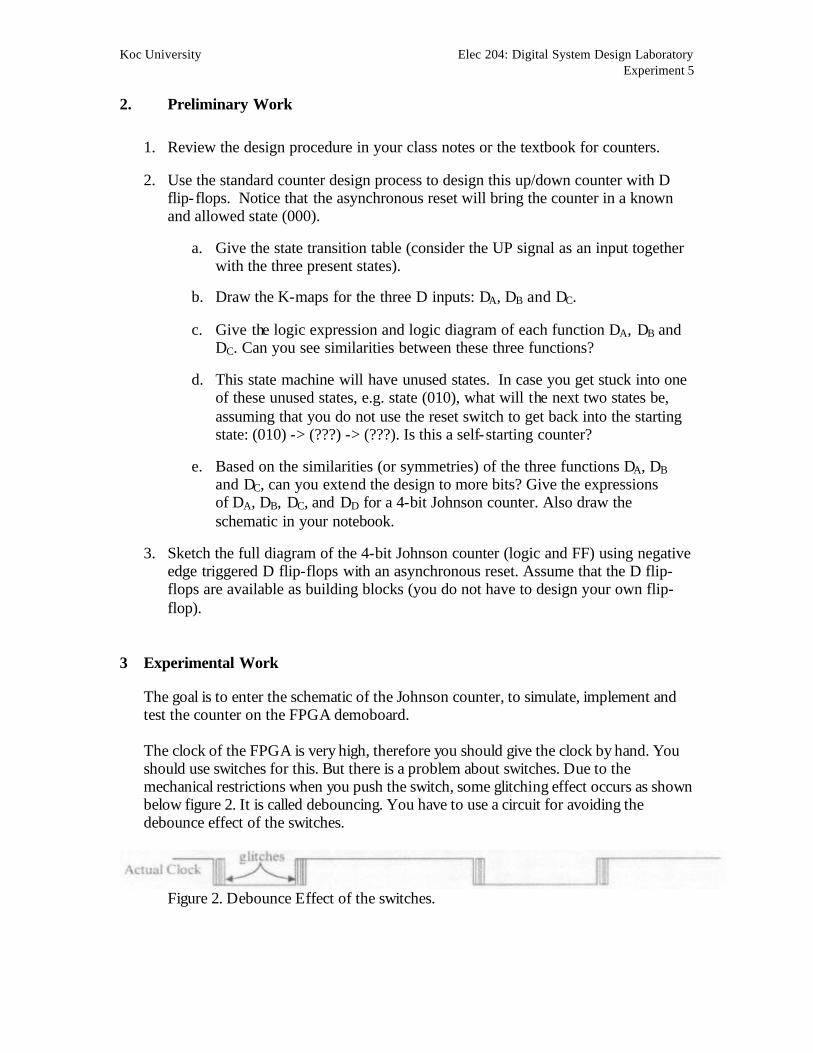
The goal is to enter the schematic of the Johnson counter, to simulate, implement and test the counter on the FPGA demoboard. The clock of the FPGA is very high, therefore you should give the clock by hand. You should use switches for this. But there is a problem about switches. Due to the mechanical restrictions when you push the switch, some glitching effect occurs as shown below figure 2. It is called debouncing. You have to use a circuit for avoiding the debounce effect of the switches.
Figure 2. Debounce Effect of the switches.
Koc University Elec 204: Digital System Design Laboratory Experiment 5
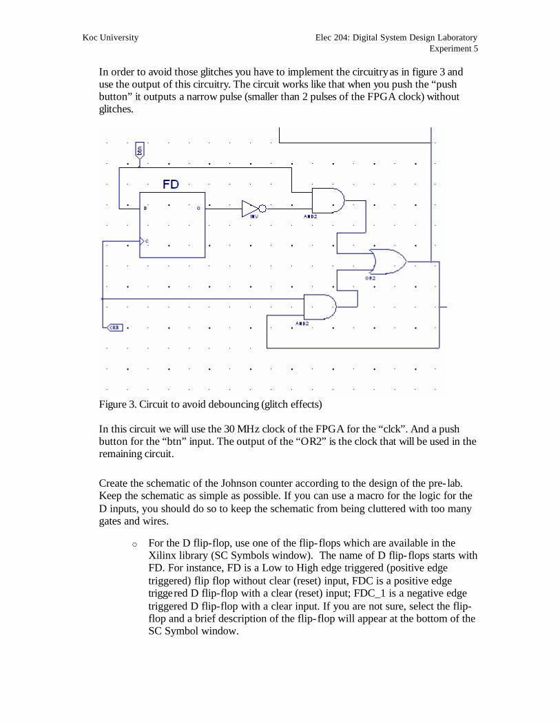
In order to avoid those glitches you have to implement the circuitry as in figure 3 and use the output of this circuitry. The circuit works like that when you push the “push button” it outputs a narrow pulse (smaller than 2 pulses of the FPGA clock) without glitches.
Figure 3. Circuit to avoid debouncing (glitch effects) In this circuit we will use the 30 MHz clock of the FPGA for the “clck”. And a push button for the “btn” input. The output of the “OR2” is the clock that will be used in the remaining circuit. Create the schematic of the Johnson counter according to the design of the pre- lab. Keep the schematic as simple as possible. If you can use a macro for the logic for the D inputs, you should do so to keep the schematic from being cluttered with too many gates and wires.
o For the D flip-flop, use one of the flip-flops which are available in the Xilinx library (SC Symbols window). The name of D flip-flops starts with FD. For instance, FD is a Low to High edge triggered (positive edge triggered) flip flop without clear (reset) input, FDC is a positive edge triggered D flip-flop with a clear (reset) input; FDC_1 is a negative edge triggered D flip-flop with a clear input. If you are not sure, select the flip-flop and a brief description of the flip-flop will appear at the bottom of the SC Symbol window.
Koc University Elec 204: Digital System Design Laboratory Experiment 5
o You will need a clock to advance the counter. There is a clock inside the PEGASUS board. But it is too fast you will use it by adjusting the ucf file of the Xilinx project for building Figure 3 and then your clock will be the output of OR2 gate in the figure 3.
o The state of the counter will be displayed on the 7-segment LED display. Design the decoder for the display or you may use your old design as a macro.
o You may use of the logic switches as UP/DOWN control and the RESET signal.
4 Assessment You have to hand in a lab report that contains the following:
• Course Title, Lab title, your names and date
• Section on the preliminary explaining the design of each block and giving the answers to each task.
• Section on the lab experiment:
a. Brief description of the goals. b. Brief explanation of the design approach and the overall schematic. c. Copy of the schematics (as a screen capture). Label the schematics
and comment on the source code. d. Logic simulation (screen capture of the waveforms; label the
outputs to prove that the circuit functions properly). e. Discussion of the results indicating that the circuit functions
properly. • Conclusion and discussion.