Embed Size (px)
Citation preview

Eindhoven University of Technology
MASTER
Exploration of low-power viterbi decoders design for low-throughput application
Lu, C.
Award date:2016
DisclaimerThis document contains a student thesis (bachelor's or master's), as authored by a student at Eindhoven University of Technology. Studenttheses are made available in the TU/e repository upon obtaining the required degree. The grade received is not published on the documentas presented in the repository. The required complexity or quality of research of student theses may vary by program, and the requiredminimum study period may vary in duration.
General rightsCopyright and moral rights for the publications made accessible in the public portal are retained by the authors and/or other copyright ownersand it is a condition of accessing publications that users recognise and abide by the legal requirements associated with these rights.
• Users may download and print one copy of any publication from the public portal for the purpose of private study or research. • You may not further distribute the material or use it for any profit-making activity or commercial gain
Take down policyIf you believe that this document breaches copyright please contact us providing details, and we will remove access to the work immediatelyand investigate your claim.
Download date: 22. Jun. 2018
Exploration of Low-powerViterbi Decoders Design
for Low-throughputApplication
Master Thesis
Chunqiu Lu
Department of Mathematics and Computer ScienceSystem Architecture and Networking Group
Supervisors:C.H. (Kees) van Berkel
Pepijn BoerM.C.W. (Marc) Geilen
Eindhoven, July 2016

Abstract
The IEEE 802.11ah is a long range 802.11 Wireless Local Area Network (WLAN) standard. Itaims to achieve a cost-effective and large scale wireless network for Internet of Things (IoT)applications. Convolutional encoding is an important process to provide error-correcting codes forthe wireless transmission in a 802.11ah transmitter. This thesis work explores the digital integratedcircuit (IC) design and implementation of a low-power and small-area convolutional decoder bythe Viterbi Algorithm for the receiver to fit the low-throughput and low-power requirement of802.11ah standard.
After investigating different architectures and algorithms to save the power and area, thepromising designs are implemented with the Cadence digital IC design tool using the TSMC40nm technology at 1.1V supply voltage. To fulfill the current project requirements, 5 Mb/s is thetarget throughput. The results of the Cadence front-end and back-end simulation are analyzedconcerning the power and area and also are compared with the state-of-the-art design in the lit-erature. Among all the architectures with the conventional Viterbi Algorithm, the optimal designis the fully-parallel architecture which has 247 uW power and 0.04 mm2 area at 10 MHz clock.Among all implemented algorithms based on the fully-parallel architecture with the conventionalViterbi Algorithm, the pre-traceback (PTB) algorithm are the optimal with 269 uW power and0.04 mm2 area at 5 MHz clock rate. PTB can achieve the maximum throughput (40 Mb/s) amongall designs with 40 MHz clock rate. So it is promising to be the optimal low-power design by thevoltage and clock rate scaling. The power target based on the scaling results of state-of-the-artdesigns can be achieved by two selected implementations.
Keywords. 802.11ah, IoT, low-power, Viterbi Decoder, IC design
ii Exploration of Low-power Viterbi Decoders Design for Low-throughput Application

Preface
This document is the Master thesis of my graduation project for the M.Sc degree with a specializ-ation in Embedded Systems at TU Eindhoven. The project began in November 2015 and finishedin July 2016. It was carries out at IMEC in the Holst Center.
Firstly, I would like to express my sincere gratitude to my university supervisor Prof. C.H.van Berkel for the great guidance. His knowledge, patience and attitude to the science deeplyimpressed me. I would like to also thank Pepijn Boer as my company supervisor who gives methe chance to carry out my research at IMEC in the Holst Center. He guided me a lot during theresearch work and helped me improve my presentation and thesis writing. Also, my appreciationis also for dr. M.C.W. Geilen, the member of my examination committee, who gave me severalvaluable comments. In addition, I would like to appreciate my colleges in IMEC especially Evgeniand Benjamin for their help in the VLSI design. Without their help, I cannot smoothly workon my research. My gratitude is also for my friends and classmates during my work and study.Finally, I greatly appreciate the support from my parents and my girlfriend in the past years.
Lu ChunqiuEindhoven, August 2016
Exploration of Low-power Viterbi Decoders Design for Low-throughput Application iii

Contents
Contents iv
List of Figures vii
List of Tables x
Acronyms xi
1 Introduction 11.1 Background and contribution . . . . . . . . . . . . . . . . . . . . . . . . . . . . . . 11.2 IEEE 802.11ah and IoT Overview . . . . . . . . . . . . . . . . . . . . . . . . . . . . 2
1.2.1 Base-band Processing Overview . . . . . . . . . . . . . . . . . . . . . . . . . 21.2.2 Binary Convolutional Encoder and Punctuate Overview . . . . . . . . . . . 3
1.3 Design Tools Overview . . . . . . . . . . . . . . . . . . . . . . . . . . . . . . . . . . 4
2 Problem Definition 62.1 Motivation . . . . . . . . . . . . . . . . . . . . . . . . . . . . . . . . . . . . . . . . 62.2 Problem . . . . . . . . . . . . . . . . . . . . . . . . . . . . . . . . . . . . . . . . . . 62.3 Objectives . . . . . . . . . . . . . . . . . . . . . . . . . . . . . . . . . . . . . . . . . 72.4 Overview of literature study . . . . . . . . . . . . . . . . . . . . . . . . . . . . . . . 82.5 Approach . . . . . . . . . . . . . . . . . . . . . . . . . . . . . . . . . . . . . . . . . 10
3 Viterbi Decoders 123.1 Introduction . . . . . . . . . . . . . . . . . . . . . . . . . . . . . . . . . . . . . . . . 123.2 Branch Metric Unit . . . . . . . . . . . . . . . . . . . . . . . . . . . . . . . . . . . . 13
3.2.1 Maximum Likelihood Bit metrics . . . . . . . . . . . . . . . . . . . . . . . . 133.2.2 log-likelihood ratio soft bit metrics . . . . . . . . . . . . . . . . . . . . . . . 14
3.3 Path Metric Unit . . . . . . . . . . . . . . . . . . . . . . . . . . . . . . . . . . . . . 153.4 Survivor Memory Unit . . . . . . . . . . . . . . . . . . . . . . . . . . . . . . . . . . 163.5 Simulation Platform . . . . . . . . . . . . . . . . . . . . . . . . . . . . . . . . . . . 17
4 Design and implementation of architecture 194.1 Branch Metric Unit . . . . . . . . . . . . . . . . . . . . . . . . . . . . . . . . . . . . 19
4.1.1 Quantization Scheme . . . . . . . . . . . . . . . . . . . . . . . . . . . . . . . 194.1.2 Architecture Design . . . . . . . . . . . . . . . . . . . . . . . . . . . . . . . 21
4.2 Add-Compare-Select Unit . . . . . . . . . . . . . . . . . . . . . . . . . . . . . . . . 224.2.1 Precision and Normalization Scheme . . . . . . . . . . . . . . . . . . . . . . 224.2.2 Architecture Design . . . . . . . . . . . . . . . . . . . . . . . . . . . . . . . 23
4.3 Path Metric Unit . . . . . . . . . . . . . . . . . . . . . . . . . . . . . . . . . . . . . 244.3.1 Architecture Design . . . . . . . . . . . . . . . . . . . . . . . . . . . . . . . 244.3.2 Routing and Scheduler Design . . . . . . . . . . . . . . . . . . . . . . . . . 254.3.3 Analysis . . . . . . . . . . . . . . . . . . . . . . . . . . . . . . . . . . . . . . 27
4.4 Survivor Memory Unit . . . . . . . . . . . . . . . . . . . . . . . . . . . . . . . . . . 28
iv Exploration of Low-power Viterbi Decoders Design for Low-throughput Application

CONTENTS
4.4.1 Register Exchange and Traceback Algorithm . . . . . . . . . . . . . . . . . 28
4.4.2 Architecture Design . . . . . . . . . . . . . . . . . . . . . . . . . . . . . . . 29
4.4.3 Choice of Memory . . . . . . . . . . . . . . . . . . . . . . . . . . . . . . . . 32
4.5 Overall design . . . . . . . . . . . . . . . . . . . . . . . . . . . . . . . . . . . . . . . 32
5 Design of standard and adaptive algorithm 34
5.1 Traceforward algorithm . . . . . . . . . . . . . . . . . . . . . . . . . . . . . . . . . 34
5.1.1 Introduction . . . . . . . . . . . . . . . . . . . . . . . . . . . . . . . . . . . 34
5.1.2 Architecture design . . . . . . . . . . . . . . . . . . . . . . . . . . . . . . . . 35
5.1.3 Analysis . . . . . . . . . . . . . . . . . . . . . . . . . . . . . . . . . . . . . . 36
5.2 Pre-traceback algorithm . . . . . . . . . . . . . . . . . . . . . . . . . . . . . . . . . 38
5.2.1 Principle and architecture design . . . . . . . . . . . . . . . . . . . . . . . . 38
5.2.2 Analysis . . . . . . . . . . . . . . . . . . . . . . . . . . . . . . . . . . . . . . 40
5.3 Dynamic traceback length with path prediction algorithm . . . . . . . . . . . . . . 40
5.3.1 Introduction and architecture design . . . . . . . . . . . . . . . . . . . . . . 40
5.3.2 Analysis . . . . . . . . . . . . . . . . . . . . . . . . . . . . . . . . . . . . . . 41
6 Implementation, results and analysis 43
6.1 Introduction . . . . . . . . . . . . . . . . . . . . . . . . . . . . . . . . . . . . . . . . 43
6.2 Specification . . . . . . . . . . . . . . . . . . . . . . . . . . . . . . . . . . . . . . . . 43
6.3 Implementation of different architectures . . . . . . . . . . . . . . . . . . . . . . . . 44
6.3.1 Design . . . . . . . . . . . . . . . . . . . . . . . . . . . . . . . . . . . . . . . 44
6.3.2 Back-end results and analysis . . . . . . . . . . . . . . . . . . . . . . . . . . 45
6.3.3 Comparison of front-end and back-end results . . . . . . . . . . . . . . . . . 47
6.4 Implementation of standard algorithm . . . . . . . . . . . . . . . . . . . . . . . . . 48
6.4.1 Design . . . . . . . . . . . . . . . . . . . . . . . . . . . . . . . . . . . . . . . 48
6.4.2 Back-end results and analysis . . . . . . . . . . . . . . . . . . . . . . . . . . 48
6.4.3 Comparison of front-end and back-end results . . . . . . . . . . . . . . . . . 50
6.5 Implementation of adaptive algorithm . . . . . . . . . . . . . . . . . . . . . . . . . 51
6.5.1 Design . . . . . . . . . . . . . . . . . . . . . . . . . . . . . . . . . . . . . . . 51
6.5.2 Back-end results and analysis . . . . . . . . . . . . . . . . . . . . . . . . . . 51
6.6 Comparison of all implementations . . . . . . . . . . . . . . . . . . . . . . . . . . . 52
7 Conclusion and recommendations 55
7.1 Conclusion . . . . . . . . . . . . . . . . . . . . . . . . . . . . . . . . . . . . . . . . 55
7.2 Recommendations . . . . . . . . . . . . . . . . . . . . . . . . . . . . . . . . . . . . 56
Bibliography 57
Appendix 61
A Introduction to Viterbi Algorithm 61
B Conventional Viterbi Algorithm 62
C Flow chart of dynamic truncation length and path prediction algorithm 63
D Routing of fully parallel, shared factor 2 and 4 64
E Analysis of the front-end simulation results 66
E.1 Front-end results and analysis of three architectures . . . . . . . . . . . . . . . . . 66
E.2 Front-end results and analysis of two standard algorithms . . . . . . . . . . . . . . 69
E.3 Front-end results and analysis of the adaptive algorithm . . . . . . . . . . . . . . . 71
Exploration of Low-power Viterbi Decoders Design for Low-throughput Application v

CONTENTS
F Comparison of results by the front-end and back-end synthesis of differentarchitectures 73
G Comparison of results by the front-end and back-end synthesis of two standardalgorithms 75
H Comparison of results by the front-end and back-end synthesis of adaptivealgorithms 77
vi Exploration of Low-power Viterbi Decoders Design for Low-throughput Application

List of Figures
1.1 Simplified base-band processing flow of 802.11ah at transmitter and receiver sides . 21.2 Convolutional encoder (K=7) . . . . . . . . . . . . . . . . . . . . . . . . . . . . . . 31.3 An example of the trellis . . . . . . . . . . . . . . . . . . . . . . . . . . . . . . . . . 41.4 Punctuating scheme to achieve coding rate 3/4 . . . . . . . . . . . . . . . . . . . . 41.5 Cadence Digital IC design flow . . . . . . . . . . . . . . . . . . . . . . . . . . . . . 5
2.1 Figure of Merit . . . . . . . . . . . . . . . . . . . . . . . . . . . . . . . . . . . . . . 82.2 Design space for the Branch Metric Unit and Path Metric Unit . . . . . . . . . . . 92.3 Design space for Survivor Memory Unit (SMU) . . . . . . . . . . . . . . . . . . . . 10
3.1 Simplified base-band processing flow of 802.11ah at transmitter and receiver sides . 123.2 the BER performance with hard and soft decision decoding . . . . . . . . . . . . . 153.3 Illustration of ACSU in a PMU . . . . . . . . . . . . . . . . . . . . . . . . . . . . . 163.4 Truncation property [1] . . . . . . . . . . . . . . . . . . . . . . . . . . . . . . . . . 173.5 Structure of the Viterbi Decoder . . . . . . . . . . . . . . . . . . . . . . . . . . . . 173.6 Simulation Platform based on Matlab . . . . . . . . . . . . . . . . . . . . . . . . . 18
4.1 An example of a q=3 quantization . . . . . . . . . . . . . . . . . . . . . . . . . . . 204.2 Comparison of different input quantization schemes with QPSK in the AWGN channel 204.3 Comparison of different input quantization schemes with 16QAM in the AWGN
channel . . . . . . . . . . . . . . . . . . . . . . . . . . . . . . . . . . . . . . . . . . 214.4 Design of Branch Metric Unit . . . . . . . . . . . . . . . . . . . . . . . . . . . . . . 224.5 (a)2-way Add-Compare-Select Unit (ACSU) (b)Radix-2 trellis (c)Radix-2 ACSU [2] 244.6 Architecture of Path Metric Unit . . . . . . . . . . . . . . . . . . . . . . . . . . . . 254.7 An example of shared-4 architecture for 802.11ah standard . . . . . . . . . . . . . 254.8 Local routing example . . . . . . . . . . . . . . . . . . . . . . . . . . . . . . . . . . 264.9 (a)Implementation of local routing (b) Example of the implementation . . . . . . . 264.10 Control unit design . . . . . . . . . . . . . . . . . . . . . . . . . . . . . . . . . . . . 274.11 Critical path of a VD . . . . . . . . . . . . . . . . . . . . . . . . . . . . . . . . . . 284.12 VLSI design for register exchange algorithm (REA) [3] . . . . . . . . . . . . . . . . 294.13 the BER performance with different traceback length . . . . . . . . . . . . . . . . . 304.14 the BER performance with different traceback start state scheme . . . . . . . . . . 314.15 Survivor Memory Unit architecture design . . . . . . . . . . . . . . . . . . . . . . . 314.16 Saving percentage of memory access energy per bit . . . . . . . . . . . . . . . . . . 324.17 Overall architecture design . . . . . . . . . . . . . . . . . . . . . . . . . . . . . . . 33
5.1 TF Example . . . . . . . . . . . . . . . . . . . . . . . . . . . . . . . . . . . . . . . . 355.2 (a)Design of Add-Compare-Select Unit (ACSU) for TF (b)Design of Processing
Element (PE) . . . . . . . . . . . . . . . . . . . . . . . . . . . . . . . . . . . . . . . 365.3 Memory access of sliding window TF algorithm [4] . . . . . . . . . . . . . . . . . . 365.4 Design of Add-Compare-Select Unit (ACSU) for sliding traceforward (TF) . . . . . 375.5 Saving percentage of memory access energy per bit by TF . . . . . . . . . . . . . . 38
Exploration of Low-power Viterbi Decoders Design for Low-throughput Application vii

LIST OF FIGURES
5.6 PTB example . . . . . . . . . . . . . . . . . . . . . . . . . . . . . . . . . . . . . . . 39
5.7 (a)Design of Add-Compare-Select Unit (ACSU) for PTB (b)Design of ProcessingElement (PE) . . . . . . . . . . . . . . . . . . . . . . . . . . . . . . . . . . . . . . . 39
5.8 Illustration of the DTBL algorithm . . . . . . . . . . . . . . . . . . . . . . . . . . . 41
5.9 Design of Survivor Memory Unit (SMU) . . . . . . . . . . . . . . . . . . . . . . . . 41
5.10 Memory access saving with the DTBL algorithm . . . . . . . . . . . . . . . . . . . 42
6.1 Comparison of power distribution between three architectures by back-end synthesis 46
6.2 Comparison of power distribution of the PE between three architectures by back-end synthesis . . . . . . . . . . . . . . . . . . . . . . . . . . . . . . . . . . . . . . . 46
6.3 Comparison of power distribution of minor modules between three architectures byback-end synthesis . . . . . . . . . . . . . . . . . . . . . . . . . . . . . . . . . . . . 46
6.4 Comparison of area distribution between three architectures by back-end synthesis 47
6.5 Comparison of area distribution of the PE between three architectures by back-endsynthesis . . . . . . . . . . . . . . . . . . . . . . . . . . . . . . . . . . . . . . . . . . 47
6.6 Area distribution comparison of minor modules between three architectures by back-end synthesis . . . . . . . . . . . . . . . . . . . . . . . . . . . . . . . . . . . . . . . 47
6.7 Comparison of power distribution between 2 standard algorithms by back-end syn-thesis . . . . . . . . . . . . . . . . . . . . . . . . . . . . . . . . . . . . . . . . . . . 49
6.8 Comparison of power distribution of the PE between 2 standard algorithms byback-end synthesis . . . . . . . . . . . . . . . . . . . . . . . . . . . . . . . . . . . . 49
6.9 Power distribution comparison of minor modules between 2 standard algorithms byback-end synthesis . . . . . . . . . . . . . . . . . . . . . . . . . . . . . . . . . . . . 49
6.10 Comparison of area distribution between 2 standard algorithms by back-end synthesis 50
6.11 Comparison of area distribution of the PE between 2 standard algorithms by back-end synthesis . . . . . . . . . . . . . . . . . . . . . . . . . . . . . . . . . . . . . . . 50
6.12 Area distribution comparison of minor modules between 2 standard algorithms byback-end synthesis . . . . . . . . . . . . . . . . . . . . . . . . . . . . . . . . . . . . 50
6.13 Comparison of power distribution between the DTBL and shared-2 by back-endsynthesis . . . . . . . . . . . . . . . . . . . . . . . . . . . . . . . . . . . . . . . . . . 51
6.14 Power distribution of minor modules between the DTBL and shared-2 by back-endsynthesis . . . . . . . . . . . . . . . . . . . . . . . . . . . . . . . . . . . . . . . . . . 51
6.15 Memory access saving with DTB algorithm based on shared-2 architecture . . . . . 52
6.16 Comparison of area distribution of the PE between the DTBL and shared-2 byback-end synthesis . . . . . . . . . . . . . . . . . . . . . . . . . . . . . . . . . . . . 52
6.17 Comparison of energy per bit with maximum clock frequency . . . . . . . . . . . . 54
7.1 Final result . . . . . . . . . . . . . . . . . . . . . . . . . . . . . . . . . . . . . . . . 55
A.1 Viterbi Algorithm [5] . . . . . . . . . . . . . . . . . . . . . . . . . . . . . . . . . . 61
C.1 Illustration of (a) dynamic truncation length (b)path prediction algorithm [6] . . . 63
E.1 Comparison of power distribution between three architectures by front-end synthesis 66
E.2 Comparison of power distribution of the PE between three architectures by front-end synthesis . . . . . . . . . . . . . . . . . . . . . . . . . . . . . . . . . . . . . . . 67
E.3 Comparison of power distribution of minor modules between three architectures byfront-end synthesis . . . . . . . . . . . . . . . . . . . . . . . . . . . . . . . . . . . . 67
E.4 Comparison of area distribution between three architectures by front-end synthesis 67
E.5 Comparison of area distribution of the PE between three architectures by front-endsynthesis . . . . . . . . . . . . . . . . . . . . . . . . . . . . . . . . . . . . . . . . . . 68
E.6 Comparison of area distribution of minor modules between three architectures byfront-end synthesis . . . . . . . . . . . . . . . . . . . . . . . . . . . . . . . . . . . . 68
viii Exploration of Low-power Viterbi Decoders Design for Low-throughput Application

LIST OF FIGURES
E.7 Comparison of power distribution between 2 standard algorithms by front-end syn-thesis . . . . . . . . . . . . . . . . . . . . . . . . . . . . . . . . . . . . . . . . . . . 69
E.8 Comparison of power distribution of the PE between 2 standard algorithms byfront-end synthesis . . . . . . . . . . . . . . . . . . . . . . . . . . . . . . . . . . . . 69
E.9 Power distribution comparison of minor modules between 2 standard algorithms byfront-end synthesis . . . . . . . . . . . . . . . . . . . . . . . . . . . . . . . . . . . . 70
E.10 Comparison of area distribution between 2 standard algorithms by front-end synthesis 70E.11 Comparison of area distribution of the PE between 2 standard algorithms by front-
end synthesis . . . . . . . . . . . . . . . . . . . . . . . . . . . . . . . . . . . . . . . 71E.12 Area distribution comparison of minor modules between 2 standard algorithms by
front-end synthesis . . . . . . . . . . . . . . . . . . . . . . . . . . . . . . . . . . . . 71E.13 Comparison of power distribution of the PE between the DTBL and shared-2 by
front-end synthesis . . . . . . . . . . . . . . . . . . . . . . . . . . . . . . . . . . . . 72E.14 Power distribution comparison of minor modules between the DTBL and shared-2
by front-end synthesis . . . . . . . . . . . . . . . . . . . . . . . . . . . . . . . . . . 72E.15 Comparison of area distribution between the DTBL and shared-2 by front-end syn-
thesis . . . . . . . . . . . . . . . . . . . . . . . . . . . . . . . . . . . . . . . . . . . 72
F.1 Comparison of power distribution with front-end and back-end synthesis . . . . . . 73F.2 Comparison of power distribution of PEs with front-end and back-end synthesis . . 74F.3 Comparison of area distribution with front-end and back-end synthesis . . . . . . . 74F.4 Comparison of area distribution of PEs with front-end and back-end synthesis . . . 74
G.1 Comparison of power distribution with front-end and back-end synthesis . . . . . . 75G.2 Comparison of power distribution of PEs with front-end and back-end synthesis . . 75G.3 Comparison of area distribution with front-end and back-end synthesis . . . . . . . 76G.4 Comparison of area distribution of PEs with front-end and back-end synthesis . . . 76
H.1 Comparison of area distribution between DTBL and shared-2 by front-end andback-end synthesis . . . . . . . . . . . . . . . . . . . . . . . . . . . . . . . . . . . . 77
H.2 Comparison of area distribution between DTBL and shared-2 by front-end andback-end synthesis . . . . . . . . . . . . . . . . . . . . . . . . . . . . . . . . . . . . 77
Exploration of Low-power Viterbi Decoders Design for Low-throughput Application ix

List of Tables
1.1 S1G MCSs for 1 MHz, Nss = 1 . . . . . . . . . . . . . . . . . . . . . . . . . . . . . 3
3.1 Comparison of maximum likelihood and LLR soft bit metrics . . . . . . . . . . . . 15
5.1 Comparison of decoding latency . . . . . . . . . . . . . . . . . . . . . . . . . . . . . 38
6.1 Specification of three architectures . . . . . . . . . . . . . . . . . . . . . . . . . . . 456.2 Specification of 3 standard algorithms . . . . . . . . . . . . . . . . . . . . . . . . . 486.3 Comparison of all the implementations by back-end synthesis . . . . . . . . . . . . 536.4 Comparison of all the clock frequency and memory size . . . . . . . . . . . . . . . 54
D.1 Scheduler in the local routing of PMU for (a) shared factor 2 and (b) shared factor 4 64D.2 Global routing table of fully parallel architecture . . . . . . . . . . . . . . . . . . . 65D.3 Global routing table of (a) shared factor 2 and (b) shared factor 4 . . . . . . . . . 65
x Exploration of Low-power Viterbi Decoders Design for Low-throughput Application
Acronyms
16-QAM 16-quadrature amplitude modulation.
ACS Add-Compare-Select.
ACSU Add-Compare-Select Unit.
ASIC application-specific integrated circuit.
AWGN additive white Gaussian noise.
BCC binary convolutional coding.
BER bit error rate.
BICM Bit-Interleaved Coded Modulation.
BM Branch Metric.
BMU Branch Metric Unit.
BPSK binary phase shift keying.
DC decoding read.
DTBL dynamic traceback length.
EDA electronic design automation.
FILO first-in last-out.
HDL hardware-define language.
IC integrated circuit.
IoT Internet of Things.
LLR log-likelihood ratio.
MCS modulation and coding scheme.
OFDM orthogonal frequency-division multiplexing.
PE Processing Element.
PM Path Metric.
Exploration of Low-power Viterbi Decoders Design for Low-throughput Application xi

Acronyms
PMU Path Metric Unit.
PTB pre-traceback.
QPSK quadrature phase shifting keying.
REA register exchange algorithm.
RTL register-transfer language.
S1G sub 1 GHz.
SCM standard cell-based memory.
SM State Metric.
SMU Survivor Memory Unit.
SNR signal-to-noise ratio.
TB traceback read.
TBA traceback algorithm.
TF traceforward.
TRR traceback recursion rate.
TSMC Taiwan Semiconductor Manufacturing Company.
ULP ultra-low-power.
VA Viterbi Algorithm.
VD Viterbi Decoder.
VLSI very-large-scale integration.
WLAN Wireless Local Area Network.
WR write-decisions.
xii Exploration of Low-power Viterbi Decoders Design for Low-throughput Application

Chapter 1
Introduction
1.1 Background and contribution
The Internet of Things (IoT) is one of the hottest fields in recent years. The world’s attention isattracted by its concept that establishes a smart network of household appliances, vehicles andother physical items. Inevitably, new theories and methods need to be developed to fulfill its re-quirements, thus the IEEE 802.11 ah standard are proposed to provide an efficient wireless networkprotocol in the application context of the IoT. IMEC at Holst Centre, Netherlands is researchingultra-low-power (ULP) design and development of the radio integrated circuit transceivers for the802.11ah standard. This thesis work aims to design and implement low-power and small-areaViterbi Decoders to fit the requirement of the IEEE 802.11 ah standard and the application in theIoT field with the Taiwan Semiconductor Manufacturing Company (TSMC) 40 nm technology.
The contribution of this work is that it systematically studies the principle and integratedcircuit (IC) design of Viterbi Decoders. Each component of the Viterbi Decoder (VD) is invest-igated and designed for low-power and small-area purpose. In addition, based on the literaturestudy, the performance comparison is made among different architectures and algorithms. Thenseveral promising designs are implemented by the Cadence tool. The simulation results concerningbit error rate (BER), power and area are compared and analyzed. The optimal architecture andalgorithms are selected which completely satisfy the target.
The contents of this thesis are organized as the following. Chapter 1 introduces the generalbackground and contribution of this thesis work as well as several important related conceptsincluding 802.11ah, IoT and design tools. Chapter 2 briefly illustrates the motivation and problemdefinition to figure out the issues to be solved. In addition, the related literature is reviewed andthe approach and detail objectives of this thesis work are described. Chapter 3 discusses theprinciple of Viterbi Decoders and introduces the Matlab simulation chain. In the chapter 4, theconventional very-large-scale integration (VLSI) design and implementation are described in detail.Chapter 5 discusses the theory and design of several noval algorithms to save power and area. Theimplementation of promising designs are introduced in Chapter 6. The simulation results are alsoillustrated, compared and analyzed in this chapter. The last chapter concludes all the work andlists several recommendations for the future work.
Exploration of Low-power Viterbi Decoders Design for Low-throughput Application 1

CHAPTER 1. INTRODUCTION
1.2 IEEE 802.11ah and IoT Overview
IEEE 802.11ah [7] is a new long range 802.11 Wireless Local Area Network (WLAN) standard,operating at sub 1 GHz (S1G) bands. Compared to the current IEEE 802.11 WLAN at 2.4GHz and 5 GHz bands, the low frequency bands of the 802.11ah extend the limitation of thetransmission range and it can achieve cost-effective and large scale wireless networks, as describedin [8]. It can be used in various situations, such as the large scale sensor network, outdoor WiFifor the cellular traffic offloading.
The IoT is a network with physical devices which can collect, process and exchange data.Consisting with scattered sensors and actuators, important requirements for the communicationprotocol are low data rate, low-power and long-range. The characteristic of 802.11ah can supportthe concept of the IoT, thus 802.11ah standard is also regarded as an IoT standard.
1.2.1 Base-band Processing Overview
Figure 1.1 shows a simplified base-band processing flow of the 802.11ah at transmitter and receiversides in the physical layer which omits the parts that is not concerned in this thesis work. The flowworks as that, at the transmitter side, the source bits are firstly encoded and then punctuated ata certain pattern. The standard uses the Bit-Interleaved Coded Modulation (BICM) based on [9],therefore bits are bit-by-bit interleaved and then mapped into symbols, according to the constella-tion mappings in the standard. After that, the complex symbols are modulated by an orthogonalfrequency-division multiplexing (OFDM) modulator and then transmitted to the receiver throughthe wireless communication channel. At the receiver side, the received bits are first processed bydemodulation and de-interleaving. Then a decoder is used to correct the channel errors to obtaindecoded bits.
Figure 1.1: Simplified base-band processing flow of 802.11ah at transmitter and receiver sides
According to the description in [7], the sub 1 GHz (S1G) physical (PHY) data sub-carriers aremodulated (also demodulated) with binary phase shift keying (BPSK), quadrature phase shiftingkeying (QPSK), 16-quadrature amplitude modulation (16-QAM), 64-QAM and 256-QAM. Theencoding and decoding apply the forward error correction (FEC) including the binary convolutionalcoding (BCC) and low-density-parity-check (LDPC) coding, with coding rates of 1/2, 2/3, 3/4and 5/6. A list of modulation and coding scheme (MCS) is illustrated in Table 1.1 with the singlespatial stream (Nss = 1) and 1 MHz channel.
2 Exploration of Low-power Viterbi Decoders Design for Low-throughput Application

CHAPTER 1. INTRODUCTION
Table 1.1: S1G MCSs for 1 MHz, Nss = 1
1.2.2 Binary Convolutional Encoder and Punctuate Overview
The binary convolutional coding (BCC) encoder of the IEEE 802.11 standard in [10] uses theindustry-standard generator polynomials, g0=1338 and g1=1718 of rate 1/2, as shown in figure1.2. The following equation 1.1 shows the encoding formula. The coding rate R is defined as theratio of the number of source bits over the number of encoded bits. The memory of the encoderis 6 and the constraint length K is defined as the memory size plus 1, which is 7 in the standard.
A : b0,n = dn−6 ⊕ dn−5 ⊕ dn−3 ⊕ dn−2 ⊕ dnB : b1,n = dn−6 ⊕ dn−3 ⊕ dn−2 ⊕ dn−1 ⊕ dn
(1.1)
Figure 1.2: Convolutional encoder (K=7)
In addition, the decimal number represented by the encoder memory is defined as the stateof the encoder at time n is, shown in the equation 1.2.
sn =
K−1∑j=1
dn−j ∗ 2K−j−1 (1.2)
Therefore, the encoding process can be regarded as a state machine, which can be extendedas a trellis graph. Figure 1.3 illustrates an example of the trellis, with a rate 1/2 and K=3. Eacharray represents a state transfer and each column shows all the states at one encoding step.
Exploration of Low-power Viterbi Decoders Design for Low-throughput Application 3

CHAPTER 1. INTRODUCTION
Figure 1.3: An example of the trellis
In the 802.11ah standard, the higher coding rate is achieved by puncturing in a specificscheme, shown in figure 1.4 which takes rate 3/4 as an example. Firstly, an 8 bits source streamare encoded to 16 encoded bits and then the 4th and 5th (stolen bits) are punctuated at every 6bits. At the receiver side, the received bit sequence is de-punctuated by inserting dummy bits inthe same scheme.
Figure 1.4: Punctuating scheme to achieve coding rate 3/4
1.3 Design Tools Overview
To achieve high performance, the digital application-specific integrated circuit (ASIC) design flowis applied and Cadence software is used as an electronic design automation (EDA) tool with theTaiwan Semiconductor Manufacturing Company (TSMC) 40 nm technology library. The figure1.5 shows the digital IC design work flow.
After the functional and logical design, a set of register-transfer language (RTL) program bya hardware-define language (HDL) is written whose behavior shall be verified with the CadenceNCsim. Once the behavioural verification is finished, Cadence RTLcompiler is applied to logical
4 Exploration of Low-power Viterbi Decoders Design for Low-throughput Application

CHAPTER 1. INTRODUCTION
Figure 1.5: Cadence Digital IC design flow
synthesize the design and generate a gate-level netlist together with the TSMC 40 nm libraryand user-defined constraints (timing, power, etc.). Then NCsim is used to verify the behaviour ofthe netlist and check whether its performance can satisfy constraints. The previous procedure iscalled front-end simulation, which focuses on the verification of the logic. The power consumptionand area can be coarsely estimated at by PrimeTime and RTLcompiler respectively the end of thefront-end simulation.
Cadence Encounter continues the following steps for the physical design, called the back-end simulation and more complicated factors including routing, physical dimension, delay areconsidered. The design steps contain floor-planning, placement, clock tree synthesis, route andpost-route optimization. The layout is generated at the end. At this stage, a much more accuratepower and area can be obtained.
Exploration of Low-power Viterbi Decoders Design for Low-throughput Application 5

Chapter 2
Problem Definition
This chapter describes the motivation of this theis work and application context of the targetdesign in the 802.11 ah standard. Also, the problem definition is figured out to illustrate a clearobjectives. The related literature is reviewed especially the low-power and small-area methods toprovide possible solutions for the further study. The last section shows the approach in detail.
2.1 Motivation
IMEC at Holst Centre, Netherlands is researching the ultra-low-power (ULP) design and develop-ment of the radio integrated circuit transceivers for the 802.11ah standard, aimed at transmittingand receiving data from various sources with low power. The digital application-specific integratedcircuit (ASIC) design flow with Taiwan Semiconductor Manufacturing Company (TSMC) 40 nmtechnology is used in the development to achieve high performance. In the 802.11ah standard,after the data is encoded, processed and transmitted, the received signal needs to be recoveredat the receiver side by a series of operation. The convolutional decoding is an important processwhich corrects the error and decodes received bits. The assignment aims at investigating binaryconvolutional coding (BCC) decoders for the use in ULP radio ICs.
The 802.11ah standard aims to be applied in the long transmission range of the WLAN andachieve cost-effective and large scale wireless networks, especially for the IoT. The main require-ments include low-power consumption and small-area due to the limited power and area capacityin the application context. In addition, the transceiver is required to support the modulation andcoding scheme (MCS) idx 0 to 5 in Table 1.1, which should achieve around maximum 2.7 Mbpsthroughput. Furthermore, according to the standard [7], decoding by the Viterbi Algorithm/De-coder is recommended. Therefore, the general target is to design and implement a low-throughput,low-power, small-area IC of a Viterbi Decoder (VD) for the 802.11ah standard.
2.2 Problem
A soft-decision VD (aka soft decoder or soft decoding) use the reliability of each bit as the inputsequence while a hard-decision VD (aka hard decoder or hard decoding) uses logical value of eachbit as the input sequence. It has been known that a soft-decision VD achieve about 2dB morecoding gain than a hard-decision VD. Thus the soft decoder is usually used for better bit error
6 Exploration of Low-power Viterbi Decoders Design for Low-throughput Application
CHAPTER 2. PROBLEM DEFINITION
rate (BER) performance and higher sensitivity of the received signal power. However, more thanone bit is needed to represent the reliability of each input bit, compared to the logical value input.So the soft decoder operates more bits during the decoding and thus consumes more power andarea which limits its usage in the IoT standard. Therefore the main problem is how to design asoft decoder that consumes low-power and small-area as much as possible with acceptable BERperformance. More precisely, the following problems need to be solved in this thesis work.
1. Based on the previous work of soft decoders, how much is the expected power consumptionwith current 40nm technology? To achieve low-power and small-area in the similar applic-ation context, what kind of architectures and algorithms have been used before? How toinnovate and implement those designs in the ICs to optimize the trade-off between area,power and BER?
The previous work should be reviewed, focusing on the power performance. For a faircomparison, all the power will be scaled and normalized to energy per bit and an accuratetarget of the power shall be determined.
2. What kind of architectures and algorithms fits the requirement of the application contextfor this thesis work? Based on the requirement, suitable architectures and algorithms needto be proposed and compared in terms of the power and the area etc.
3. For a promising design plan, how to implement the IC and evaluate its power, area andBER by the software simulation? What is the accuracy of the results? What kinds offactors influence the simulation accuracy?
Cadence tools should be used to implement the IC design. After the system behaviouraldescription by the register-transfer language (RTL), the front-end synthesis is used for func-tional verification and evaluation of the area and power. Then after the floorplan placementand layout configuration, the back-end synthesis is used also for the physical verificationand evaluation. The results of the front-end and back-end simulation should be comparedand analyzed to evaluate the accuracy. Also, the area and power will be normalized andcompared with that of the state-of-art design based on the previous design review.
2.3 Objectives
To answer the first problem to determine a fair target in the section 2.2 and determine an appro-priate power target, this thesis work summarizes and scales previous IC designs of the VD. Theequation to fairly scale the energy per bit is based on the scaling formula in [11], taking importantparameters into account, shown in the Equation 2.1.
Enorm = Pnorm ∗ [TH ∗N ]−1 ∗ (0.7 ∗ 8 bit/ωγ + 0.3 ∗ 128/LSMU ) (2.1)
Pnorm is the normalized power dissipation (Watt), TH is the throughput (Mb/s), N is the numberof states, ωγ is the path-metric word-length, LSMU is the survivor path memory length. ThePath Metric Unit (PMU) and Survivor Memory Unit (SMU) scale with N and TH and the powerdissipation is partitioned into 70% PMU which scales proportionally to the ωγ , and 30% SMU,which scales with the LSMU.
Pnorm = PD ∗ v2 (2.2)
Equation 2.2 shows how to scale the power dissipation which considers the supply voltagescaling factor v ( the ratio of the real supply voltage and the nominal supply voltage).
Exploration of Low-power Viterbi Decoders Design for Low-throughput Application 7

CHAPTER 2. PROBLEM DEFINITION
Figure 2.1 shows the figure of merit and predicts the trend based on the work in [2, 12, 13, 14,15, 16, 17, 6, 18, 19, 20, 21, 22, 23, 24, 25, 26]. The bottom vertical axis is the CMOS feature size(nm) and the horizontal axis is the scaled energy per bit (nJ/bit/state). The upper vertical axisindicates the standard nominal supply voltage of the corresponding technology feature size. Topredict the trend, two curves (black curve and red dashed curve) are drawn based on Equation 2.1and 2.2 to cover all the scaled energy per bit in different CMOS technology and supply voltage.Therefore, the target design shall achieve a scaled energy per bit per state between 0.2 and4 pJ/bit/state which is equivalent to 7 to 80 pJ/bit with 40 nm technology and nominal supplyvoltage. The equivalent power target is from 50 µW to 1000 µW. As performance results in [17, 26]are not reliable enough, the new lower bound (drawn by the red full line) is about 200 µW afterremoving those two points .Furthermore, according to the current receiver’s performance in IMECat Holst Centre, to obtain a 2dB gain of the signal detection sensitivity, the receiver antenna needsto consumes 400 µW more power. Therefore, at the same signal detection sensitivity, the overallreceiver can consume less power if the soft decoder, which can achieve about 2 dB more codinggain than hard decoder, can consume less than 400 µW. So the target power is 200 µW to 400µW. In addition, considering the Table 1.1 and possible support to more modulation and codingscheme (MCS) index in the future, the requirement throughput is 5 Mb/s.
Figure 2.1: Figure of Merit
2.4 Overview of literature study
To answer the first problem about the related work study in the section 2.2, this section introducesthe overview of the literature study. Generally, a conventional VD mainly consists of a BranchMetric Unit (BMU), a Path Metric Unit (PMU) and a Survivor Memory Unit (SMU), which willbe explained in detail in the next chapter. The work in [1, 27] presents a comprehensive analysisof different design aspects of a VD. The design space contains the three components of a VD atalgorithmic, word, bit levels.
Starting from the input of a VD with the fixed-point arithmetic, the authors in [28] studiesthe quantization loss from the additive white Gaussian noise (AWGN) channel with the BPSKand QPSK modulation and proposed a new quantization scheme. The idea is an optimal trade-offbetween the quantization bit and BER performance loss. In addition, the work in [29] applies
8 Exploration of Low-power Viterbi Decoders Design for Low-throughput Application

CHAPTER 2. PROBLEM DEFINITION
log-likelihood ratio (LLR) to calculates the Branch Metric (BM) with a soft output demodulator.The work concludes that the LLR-based method is better compared with the conventional method( maximum likelihood bit metrics).
Given the BM, the PMU operates in the Add-Compare-Select (ACS)) recursion which determ-ines the throughput and clock frequency of the VLSI implementation. To increase the throughput,several conventional methods such as pipelining can be used. However, those methods can not beapplied at the nonlinear data dependent nature of the ACS recursion. To conquer the bottleneck,[2] combines the calculation of k steps into 1 steps, called radix-2k method, which accelerates thethroughput k times at the same clock rate. Furthermore, the IC design of a VD can even achieveGb/s-level throughput in the work [30] by parallel block processing. However, as the throughputrequirement in this thesis work is just a few Mb/s-level, state-parallel and even state-sequentialarchitecture can be applied according to the work in [14] to achieve small-area and low-power.Furthermore, the work in [31, 32] modelled an efficient management architecture to schedule thecomputation of state metrics, allowing the mapping of the trellis onto an arbitrary number ofACSs with a 100% processor utilization.
Furthermore, due to continuous addition of the branch metrics in the PMU, the range of thestate metrics is potentially unbounded which may causes buffer overflow. To solve the problem,[33] applies the modulo technique to normalize the state metrics and it is the most local anduniform approach compared with other techniques. Figure 2.2 shows a summary of the designspace for the BMU and PMU.
Figure 2.2: Design space for the Branch Metric Unit and Path Metric Unit
The SMU updates and stores the decision-bits from the PMU and produce the decodedsequence. The work in [34] proposes a direct implementation architecture, called the registerexchange algorithm (REA). Although the decoded latency is short in the REA, its large wiringarea and high power consumption limits its application only within small number of states. In theapplication context of 802.11ah standard, another method called traceback algorithm (TBA) is analternative and the work in [3] derives a generalized method for the survivor memory managementto satisfy arbitrary requirements of the memory size and the number of memory access pointerswhich is called M-pointer method. Furthermore, for the low-power purpose, the traceforward(TF) and pre-traceback (PTB) algorithms are proposed in [35] to eliminate the traceback stageand reduce memory access frequency respectively.
The previous methods including the register exchange algorithm (REA), the traceback al-gorithm (TBA) as well as the TF and the PTB algorithms are called standard algorithm. Tofurther reduce the power consumption, another category method called adaptive techniques areapplied to achieve dynamic power consumption in different signal-to-noise ratio (SNR). For ex-ample, [36, 37] introduces two adaptive algorithms called T-algorithm and M-algorithm whichreduce the number of states in the calculation based on the path metrics. Those techniques can
Exploration of Low-power Viterbi Decoders Design for Low-throughput Application 9

CHAPTER 2. PROBLEM DEFINITION
dynamically adjust the number of the working ACS recursion to save the power consumption atthe costs of arithmetic overheads and the BER performance. A predictive method is proposedin [6] based on the fact that current survivor path has high possibility to re-merge to the previoussurvivor path at high SNR. An extra unit is needed to buffer the previous path and check the oc-currence of the re-merge. This method won’t result in performance loss and aim to save the powerby reducing the number of the memory access. The work in [38] derived a Scarce-State-Transition(SST) algorithm to reduce the switching activity of a VD by adding a simple pre-decoder andpre-encoder before the decoding process.
As described in [27], the benefits of the adaptive algorithms are quite dependent on thechannel and application context and all the published results are mostly based on the AWGNchannel. Experiments and simulation with accurate channel modelling in possible applicationcases are necessary when applying those algorithms. Figure 2.3 shows a summary of the designspace for the SMU.
Figure 2.3: Design space for Survivor Memory Unit (SMU)
Furthermore, to update and store the decision-bits from the PMU, an extra memory blockis needed for the traceback algorithm (TBA). According to many designs such as [27], the staticrandom-access memory (SRAM) is an option. The work in [39] introduces a noval standard cell-based memory (SCM) for the low voltage operation. Taking the TSMC 40nm technology as anexample which is the same as this thesis work. The standard cell-based memory is dramaticallybetter in the power at low voltages. To save the power, the voltage and clock frequency of theradio ICs for the 802.11ah will be scaled down in the practice. So SCM is thus very competitivewith the power dissipation for the application context (∼1k bits size) of this thesis work, comparedto commercially available macro memories.
2.5 Approach
The primary approach used in this thesis work is the literature study, mathematical analysis andsoftware simulation with electronic design automation (EDA) tools. More precisely,
1. Firstly, formulate each step of the Viterbi Algorithm in the 802.11ah standard. Then builda Matlab simulation chain to evaluate the BER at different SNR.
2. After studying various literature to research how those work design a low-power, smallarea VD in terms of architecture and algorithm for the low-throughput application context,
10 Exploration of Low-power Viterbi Decoders Design for Low-throughput Application

CHAPTER 2. PROBLEM DEFINITION
select potential algorithms by mathematical analysis, simulate and evaluate the result in theMatlab chain.
3. Meanwhile, the performance of the VD in the literature including the power, area, through-put and IC design technology will be collected, normalized and compared to derive an ap-propriate target for this thesis work.
4. Once the results works well, design and implement the algorithm with the application-specific integrated circuit (ASIC) design flow and verify the BER performance by comparingthe output with the Matlab simulator.
5. Finally, implement the selected designs by Cadence digital IC design tools. Evaluate andcompare the performance and select the optimal design. Also, compare the performancewith the target and the previous collected work.
The thesis work mainly focuses on the design of the VLSI implementation at algorithmic level.The performance, including the BER, the power and the area are simulated and obtained basedon the AWGN channel.
Exploration of Low-power Viterbi Decoders Design for Low-throughput Application 11

Chapter 3
Viterbi Decoders
This chapter discusses the principle of a conventional VD in the mathematical perspective. Theprocesses in each component, including the Branch Metric Unit (BMU), the Path Metric Unit(PMU) and the Survivor Memory Unit (SMU) are shown and modelled. A Matlab simulationchain for the further work is also introduced at the last section.
3.1 Introduction
Figure 3.1 illustrates the processing flow in a mathematical way. Consider a sequence (totally Tbits) of source bits {dn} is encoded to a sequence of bits {b1,n,b2,n} and n represents a randommember of the sequence. After the puncture, the interleaving and the modulation, a sequence ofsymbols are generated {cn}1. Assume the channel adds noise N to the symbol c, so the receivedsymbol y are
y = c + N (3.1)
Figure 3.1: Simplified base-band processing flow of 802.11ah at transmitter and receiver sides
An approach called Maximum Likelihood Sequence Estimation (MLSE) is applied to find the
source bit sequence D={dn}, which has most likely coded the received symbol sequence R={yn}.
D = arg{maxD
P (D|R)} (3.2)
1Bold represents complex value
12 Exploration of Low-power Viterbi Decoders Design for Low-throughput Application
CHAPTER 3. VITERBI DECODERS
By applying conditional probability density function (PDF) and logarithm, the formation canbe expressed as
D = arg{maxD
T−1∑n=0
log(P (dn|yn))}
where T is the length of the source bit sequence,
yn is the corresponding symbol(s) of dn
(3.3)
Since to obtain the maximum likelihood sequence for the decoding, all the possible sequencesshould be traversed. This will lead to the exponential increment of number of the traversaland calculation with the length of the sequence. Therefore, to efficiently solve the problem, theprinciple of Viterbi Algorithm (VA) [34, 40] is applied so that only the most likely path (survivorpath) needs to be remained when two paths merge in one state.
In general, the decoding procedure is that, in step 1, at each decoding step of a trellis, calculatethe probability that the transfer to a state generates the represented encoded bits by receivedsymbols, log(P (dn|yn)). Then in step 2, for each state, add the probability to the accumulatedprobability of its predecessor states, compare them and select the optimal transfer and thenaccumulate the probability. Finally, in step 3, after a certain amount of steps, traceback fromthe optimal state by retrieving its previous path and decode. Appendix A explains the theory indetail.
Define the probability of the transfer to one state as Branch Metric(BM) and the unit tocalculate it as Branch Metric Unit (BMU). Similarly, in step 2, define accumulated probabilityas Path Metric (PM), the whole calculating unit for each state as Path Metric Unit (PMU).Each calculating element is defined as Add-Compare-Select Unit (ACSU). The unit in step 3for retrieving a path(called final survivor path) and decoding is defined as Survivor MemoryUnit (SMU).
3.2 Branch Metric Unit
This section introduces two methods for calculation in the Branch Metric Unit (BMU), maximumlikelihood bit metrics and log-likelihood ratio (LLR) soft bit metrics.
3.2.1 Maximum Likelihood Bit metrics
The Branch Metric Unit (BMU) calculates the probability that the represented encoded bits byreceived symbols corresponds to a state transfer for each state. Also, because of the logarithm inequation 3.3, the probability of a state transfer is the sum of the probability of each single receivedencoded bit, which is defined as the bit metrics. In the 802.11ah standard, the application of theBit-Interleaved Coded Modulation (BICM) requires complex implementations to calculate theprobability according to description in [9].
The work in [41] proposed a decoding scheme to calculate the BM. Based on the modulationand coding scheme (MCS) in Table 1.1, assume that the in-phase and quadrature components ofa received complex symbol y consists of m interleaved bits respectively. Define y=yI + j yQ assymbol components and {yI,1,.., yI,m, yQ,1,.., yQ,m} as the bit sequence of in-phase and quadraturecomponents. For each symbol y, the bit metric of each in-phase and quadrature bit yI,k, yQ,k
Exploration of Low-power Viterbi Decoders Design for Low-throughput Application 13

CHAPTER 3. VITERBI DECODERS
(k∈ {1, ...,m}) need to be calculated. Only yI,k is discussed here as yQ,k is the same. For yI,k,
define S(0)I,k
which comprises the corresponding source symbols c before the transmission with
logical value 0 in position (I, k) and the complementary value is S(1)I,k
. So for one bit represented
by yI,k, the bit metric is
md(yI,k) = log{∑
α∈S(d)I,k
P (y|c = α)} ≈ maxα∈S(d)
I,k
log(P (y|c = α)), where d=0,1(3.4)
The equation 3.4 applies the approximation method from the work in [42] which results innegligible performance loss.
If the communication channel is the additive white Gaussian noise (AWGN) channel, theequation 3.4 can be written as
md(yI,k) =EsN0
minα∈S(d)
I,k
{|y− α|2}+ ln
√EsπN0
, where d=0,1 (3.5)
The pairs (m0,m1) of each received encoded bit are sent to the Viterbi Decoder as an inputsequence after calculation and interleaving.
3.2.2 log-likelihood ratio soft bit metrics
The obvious disadvantage of the maximum likelihood bit metric explained above is the largecalculation complexity and the storage size. To solve the problem, the work in [29] applies thelog-likelihood ratio (LLR) to calculate the bit metric.
The log-likelihood ratio (LLR) of bI,k is defined as2
LLR(yI,k) = logP [yI,k = 1|y]
P [yI,k = 0|y]= log
∑α∈S(1)
I,k
P (y|c = α)∑α∈S(0)
I,k
P (y|c = α)
≈ logmax
α∈S(1)I,k
P (y|c = α)
maxα∈S(0)
I,k
P (y|c = α)
(3.6)
The idea of the work is to use a soft-output demodulator to generate a LLR of each bit toindicate the reliability and sends to a VD as an input sequence after de-interleaving. Furthermore,the work in [29] proves that the the branch metric calculation by the equation 3.4 is equivalentto use the LLR and also proposes a simplified method to calculate the LLR. Two methods areshown in the Table 3.1.
It can be observed that the LLR soft bit metric is better which requires half of the inputmemory and has less calculation complexity. Therefore, it is applied in this thesis work. Further-more, the BER performance difference is shown in Figure 3.2. Clearly, a soft-decision VD hasaround 2dB performance gain compared to hard-decision decoding which conforms to the resultin the literature.
2Bayes rule and approximation method are applied
14 Exploration of Low-power Viterbi Decoders Design for Low-throughput Application

CHAPTER 3. VITERBI DECODERS
ML bit metrics LLR soft bitBit metric(decoded bit 0) m0 LLRBit metric(decoded bit 1) m1 −LLR
Table 3.1: Comparison of maximum likelihood and LLR soft bit metrics
Figure 3.2: the BER performance with hard and soft decision decoding
3.3 Path Metric Unit
The Path Metric Unit (PMU) adds the Branch Metric (BM) to the Path Metric (PM) of itspredecessor states for each transfer to a given state, compare them and select the optimal transferand then accumulate the probability to update its PM. In each trellis step k, a branch metric
λ(m,i)k
is defined to denote the branch metric of the m-th branch leading to state i at step k.
Furthermore, the Path Metric (PM) represents the accumulation of the branch metrics of one
specific path through the trellis of the sequence B. γ(m,i)k
represents the path metric for a branch
m leading to state i at step k, where m∈{0,..,M-1} is the branch label among the all the M pathsleading to state i.
In the PMU, a concept called state metrics γi,k is defined to represent the selected PM for the
survivor paths of the state xk=i at trellis step k. In addition, the path metrics γ(m,i)k
leading to
state xk = i are calculated by adding the state metrics of predecessor states and the correspondingbranch metrics. The predecessor state x(k-1) is decided by the state transition function Z():
xk−1 = Z(m, i) (3.7)
Which illustrates one branch path m (m ∈ 0, ..,M − 1) leading to state xk = i. Therefore,the PM is calculated as
Exploration of Low-power Viterbi Decoders Design for Low-throughput Application 15

CHAPTER 3. VITERBI DECODERS
γ(m,i)k = γZ(m,i),k−1 + λ
(m,i)k
(3.8)
The State Metric (SM) is thus calculated as
γi,k = max{γ(0,i)k , ..., γ
(M−1,i)k } (3.9)
To finally allow the Survivor Memory Unit (SMU) to retrieve the maximum likelihood pathand decode, decision-bits sequence generated by the Add-Compare-Select Unit (ACSU) of allstates and all steps need to be stored. Decision-bits, di,k, represents the bit shifted out from thestate i predecessor at time step k after a state transfer.
Figure 3.3 shows an example of the operation in an ACSU of a PMU for the binary convolu-tional coding (BCC) in 802.11ah standard. To determine the State Metric (SM) of state 32, γ32,n,
at step n, the BM of two predecessors states, λ(0,32)n and λ
(1,32)n , calculated by BMU are firstly
added to the corresponding SM, γ0,n−1 and γ1,n−1, to obtain the PM, γ(0,32)n and γ
(1,32)n . Assume
γ(0,32)n > γ
(1,32)n , so after comparing the PM, γ
(0,32)n is selected and thus the SM γ32,n = γ
(0,32)n .
Also, the decision bit is d32,n=0 for retrieving, as 0=Z(d32,n, 32).
Figure 3.3: Illustration of ACSU in a PMU
3.4 Survivor Memory Unit
The Survivor Memory Unit (SMU) is applied to retrieve a path and decode. Two problems arisein the practical decoding that firstly it is not usually the case that the end state is known in thecontinuous transmission, so how to determine the start state of a path retrieving should be solved.Second, the decoding latency and the size of SMU is proportional to the length of the trellis, it isnot practical to use a memory whose length is the same as the source bit sequence. To solve theproblem, the truncation property in the work [43, 44] is used to obtain approximate result by afixed length of decision-bits memory at the cost of inappreciable performance losses and limitedextra implementation effort.
In the Figure 3.4, N survivor paths merge at time instant k into a single state. For the trellissteps smaller than k-D, the paths will most probably merge into a single path called final survivorpath, thus it is possible to find the final survivor path starting from the optimal state at step kfor decoding. The distance D is defined as survivor depth (truncation depth). In such case, forsteps smaller than k-D, the only one final survivor path can be determined after the processing atstep k. This will possibly resulting in a fixed latency of D trellis steps for decoding the continuoustransmission. Furthermore, the survivor memory can be truncated and only a fixed number ofdecision bits needs to be stored, i.e. d(i,j) where i ∈ {0, ..., N − 1} and j ∈ {k −D, ..., k − 1, k}.
16 Exploration of Low-power Viterbi Decoders Design for Low-throughput Application

CHAPTER 3. VITERBI DECODERS
In addition, it is also possible to find the final survivor path from other random state at step k.According to the definition in [43, 44], at the step k, the procedure that the path with the optimalstate metric is chosen to determine the final survivor is called best state decoding. Otherwise, itis called fixed state decoding if an arbitrary path is chosen. With the same survivor depth, thebest state decoding performs better which needs more hardware costs to find the optimal state,compared to the fixed state decoding.
Figure 3.4: Truncation property [1]
Therefore, the general structure of the Viterbi Decoder is shown in Figure 3.5. The BranchMetric Unit (BMU) calculates the branch metrics after receiving the channel symbols and theresults value are input into the Path Metric Unit (PMU) for all states recursively. The SurvivorMemory Unit (SMU) stores and retrieves the final survivor path by decision bits for the decoding.
Figure 3.5: Structure of the Viterbi Decoder
3.5 Simulation Platform
To provide an appropriate experiment platform to assist the further study of a VD, a stableMatlab simulation platform has been built, which simulates the process at the transmitter andreceiver sides for 802.11ah standard. The platform covers the main operation including encoding,punctuation, modulation, adding noise, demodulation, quantization and decoding. Figure 3.6shows the simulation platform with the Matlab based on an example in [45].
The Matlab telecommunication toolbox is applied in the platform and the core process is theconventional Viterbi Algorithm. The appendix B shows the pseudocode. The variables in thesimulation chain are the encoded rate, the punctuation pattern, the signal-to-noise ratio (SNR),the modulation schemes, the quantization bits of received symbols and the decoded algorithms.To prepare the IC design, the platform can be used to evaluate the BER performance for a givenmethod and study the influence of different variables.
Exploration of Low-power Viterbi Decoders Design for Low-throughput Application 17

CHAPTER 3. VITERBI DECODERS
Figure 3.6: Simulation Platform based on Matlab
18 Exploration of Low-power Viterbi Decoders Design for Low-throughput Application

Chapter 4
Design and implementation ofarchitecture
This chapter discusses in detail the VLSI design of three main components of a conventional ViterbiDecoder (VD) including the quantization, precision and normalization scheme. Necessary resultsare also shown to indicate the performance at different conditions. Low-power and small-area arethe two main concerned factors and several trade-off are made based on the application contextof this thesis work.
4.1 Branch Metric Unit
Branch Metric Unit (BMU) calculates the probability that the received bits are encoded by thestate transfer to a given state and it is the smallest unit of a conventional VD concerning boththe power and area. This section introduces the quantization of its input and design architecture.
4.1.1 Quantization Scheme
Section 3.2 introduces two methods to calculate the Branch Metric (BM) which are the maximumlikelihood bit metric and the log-likelihood ratio (LLR) soft bit metric. Because of the advantage onthe storage size and calculation complexity, the LLR soft bit metrics is chosen in this thesis work.The hardware complexity of a conventional VD in the IC design depends linearly on the numberof bits of the Branch Metric (BM) and path Path Metric (PM) which are both the calculationresults of the input. Therefore the it is necessary to minimize the number of bits of input and thebit error rate (BER) performance loss to reduce the power and area by the input quantization.
According to the work in [28], uniform quantization scheme is usually applied in the bin-ary convolutional coding (BCC) decoding. Assume a sequence of the received signal is sentto a soft demodulator which outputs a sequence of unquantized LLR with a range(-∞,∞) andJi∈{sequence of LLR}. If a q-bit signed integer is used to represent Ji, so firstly map Ji to in-terval ±∆/2, ±∆3/2,...,±(2q−1)∆/2, where ∆ is the spacing. Each interval is represented by 0,±∆,±2∆, ...,±(2q−1)∆ which maps to 0, ±1,±2, ...,±(2q−1) as the quantization value. Figure 4.1shows a quantization scheme example where q=3. The idea of quantization is to efficiently ex-tend the representation range while increasing the number of representation levels by choosing
Exploration of Low-power Viterbi Decoders Design for Low-throughput Application 19

CHAPTER 4. DESIGN AND IMPLEMENTATION OF ARCHITECTURE
appropriate q and ∆. Therefore q determines the range and ∆ determines the accuracy of thequantization.
Figure 4.1: An example of a q=3 quantization
The work in [28] studies the uniform quantization and proposes a optimal quantization schemewhere q=3 and the BER loss is only 0.14dB compared to unquantized input. The parameters ofthe binary convolutional coding (BCC) is the same as this thesis work such as the encoder andtransmission channel except the modulation scheme, only BPSK and QPSK. As one symbol inthe 16QAM can represent more encoded bits, if its energy/symbol is the same as QPSK, it can beexpected more bits are needed to accurately represent the unquantized LLR. Also, to simplify thefollowing design, a uniform quantization scheme necessary for all the modulation scheme that thisthesis work supports. Simulation shall be done to evaluate the BER performance with differentcombination of q and ∆ and all modulation schemes under different signal-to-noise ratio (SNR)in the additive white Gaussian noise (AWGN) channel.
Figure 4.2 and figure 4.3 shows the simulation results with QPSK and 16QAM. It can beobserved that in QPSK, the simulator with the quantizer with q=4 and ∆=1.0 is quite closed to theunquantized LLR as input, maximum only 0.1 dB loss. For 16QAM, the BER performances usingq=4, ∆=1.0 and q=5, ∆=0.5 are almost the same which are also closed to the BER performancesusing unquantized LLR. Therefore, to save the hardware complexity and easiness of followingdesign, the uniform quantization scheme q=4, ∆=1.0 is applied.
Figure 4.2: Comparison of different input quantization schemes with QPSK in the AWGN channel
20 Exploration of Low-power Viterbi Decoders Design for Low-throughput Application

CHAPTER 4. DESIGN AND IMPLEMENTATION OF ARCHITECTURE
Figure 4.3: Comparison of different input quantization schemes with 16QAM in the AWGN channel
4.1.2 Architecture Design
In the 802.11ah standard, the binary convolutional coding (BCC) encoder rate is 1/2 and thus thereexists 4 combinations of output bits, corresponding to 4 BMs for a state at each step. The LLRsoft bit metrics is used to calculate the BM and Table 3.1 shows the calculation for bit metrics.Furthermore, for a q-bit signed integer input LLR, if the range is limited to be symmetrical, {-2q-1+1,...,2q-1-1} and thus the range of the BM is {-2q+2,...,2q-2} if two bit metrics are directlysummed up.
Because of the properties of addition and multiplication of inequalities, the result of equa-tion 3.9 won’t be changed if the BM λk
(m,i) in equation 3.8 is divided by 2 and offset by themaximum LLR, 2q-1. The range of BMs will be {0,...,2q-2} which only requires q-bit unsignedbranch metrics. So in this thesis work, the word-width of BM is 4. Compared to the usual q-bitLLR input which ranges from -2q-1 to 2q-1-1 and requires (q+1)-bit signed branch metrics, thistransform scheme has less bit and can saves the complexity of following calculation. Figure 4.4shows a straightforward design of the Branch Metric Unit (BMU) based on the work in [27]. Theoperation of division 2 is replaced by shifting. The two inputs are LLRs of received bits after thequantization and the BMU outputs four BM.
As a smallest unit in a conventional VD, the power saving techniques at circuit-level is ex-pected to be trivial for the general power consumption. Therefore, a straightforward design isenough.
Exploration of Low-power Viterbi Decoders Design for Low-throughput Application 21

CHAPTER 4. DESIGN AND IMPLEMENTATION OF ARCHITECTURE
Figure 4.4: Design of Branch Metric Unit
4.2 Add-Compare-Select Unit
As described in Section 3.3, the Path Metric Unit (PMU) applies the Add-Compare-Select (ACS)recursion, a system of non-linear recurrence equations, to calculate the state metrics with the inputBranch Metric (BM). The characteristic of the recursion determines the achievable data and clockrate of a VLSI implementation of a conventional VD. Furthermore, due to continuous addition ofthe branch metrics, the range of the state metrics is potentially unbounded. This section showsdesign of the normalization scheme and the architecture design.
4.2.1 Precision and Normalization Scheme
The width of the Path Metric (PM) determines the precision of the PMU. The work in [46] foundthat the maximum differences ∆γ
max of the state metrics is
∆γmax≤λmax*log2N (4.1)
λMax is the upper bound of the BM and N is the number of states. The work in [2] derives aequation to calculate the number of bits
γbits= dlog2 (∆γmax + k ∗ λmax)e+ 1 (4.2)
k is related to the radix-2k structure and it is 1 in this thesis work which will be explained inthe next section. Therefore, the minimum width of the PM is 8 in this thesis work.
The normalization scheme of this thesis work directly applies the techniques in the work of [33]because it is the most local and uniform approach compared to contemporary approaches in theVLSI implementation. The scheme is considered to be local if it is operated within each ACSU
22 Exploration of Low-power Viterbi Decoders Design for Low-throughput Application

CHAPTER 4. DESIGN AND IMPLEMENTATION OF ARCHITECTURE
without the information from others. If the ACSU will not be interrupted by the normalization,it is considered to be uniform.
Based on the bound in Equation 4.3, the work of [33] applies modular arithmetic normalizationapproach and the State Metric (SM) γi,k is replaced by the normalized value
γi,k ≡ (γi,k +C
2) mod C − C
2where ∆γ
max≤ C2
(4.3)
The modular arithmetic can be implemented by 2’s complement calculation, which is suitablefor the VLSI design.
Furthermore, a modified comparator is also proposed in the work [33] to determine the selec-
tion of the SM. Consider a comparison between two SM, γ1i,k and γ2
i,k, define z(γ1i,k, γ
2i,k) as the
logical result of the comparison
z(γ1i,k, γ
2i,k) =
{1, γ1
i,k ≤ γ2i,k
0, otherwise.(4.4)
Assume the width of SM is p bits and let γ1i,k =(γ1
p , ..., γ10) and γ2
i,k =(γ2p , ..., γ
20) be the two’s
complement representation of two normalized SM. In addition, define γji,k ≡γji,k mod (C/2)
which is the unsigned value of γji,k if sign bit is ignored. Then the modified comparison rule is
z(γ1i,k, γ
2i,k) = γ1
p ⊕ γ2p ⊕ y(γ1
i,k, γ2i,k)
where is y unsigned comparison function(4.5)
It can be observed that with this scheme, the normalization process is executed within eachAdd-Compare-Select Unit (ACSU). Also, the implementation of this scheme will only replace thecomparator in the convolutional ACSU, so the calculation will not be interrupted. Therefore, it islocal and uniform. The VLSI design of this normalization scheme will be introduced in the nextsection.
4.2.2 Architecture Design
According to the definition of the Path Metric (PM) and State Metric (SM) in equation 3.8 and 3.9,Figure 4.5 (a) illustrates a direct design for the ACSU, called 2-way ACSU. Furthermore, with theprecision and normalization scheme in section 4.2.1, adders are 2’s complement adders and thecomparator implements the modified comparison rule.
To further clearly represent the state transition, the state xk at step k can be written as xjand its predecessor is ix, where i is the bit shifted out of the encoder, j is the input bit and xrepresents common bits. Take the transfer from state (100000)2 to state (000001)2 as an example.Because of the input bit j=1, the i=1 is shifted out and x is (00000)2. Following such way of the
representation, the BM of the transfer from state ix to xj is thus λkixj. So the equation 3.8 and 3.9
can be written as equation 4.6. The SM of state x0 and x1 can be both calculated from the SMof common predecessor states 0x and 1x, shown in Figure 4.5 (b), which is a well-known butterflystructure and it is also called radix-2 trellis. To reduce the complexity of the global routing, thework in [2, 32] thus designs the Processing Element (PE) to implement the butterfly structurewith two 2-way ACSU inside, shown in Figure 4.5 (c). In such way, the global routing between
Exploration of Low-power Viterbi Decoders Design for Low-throughput Application 23

CHAPTER 4. DESIGN AND IMPLEMENTATION OF ARCHITECTURE
two ACSU is converted to the local routing, which reduces half of the global routing. The BM inthe figure correspond to the four outputs in the design of the BMU in section 4.1.2, so each PEcan integrate one BMU to eliminate its global routing.
γxi,k = Max{γ1x,k−1 + λjxik , γ0x,k−1 + λj′xik }
where j + j′
= 1 and j ∈ 0, 1(4.6)
Figure 4.5: (a)2-way Add-Compare-Select Unit (ACSU) (b)Radix-2 trellis (c)Radix-2 ACSU [2]
Furthermore, higher radix structure is developed in [2], which combines more steps in thePMU into one step. The chip fabrication result in [2] shows that the radix-4 design achieves anincreasing of the throughput with a factor of 1.7 and the area with a factor of 2, so the complexitydoesn’t increase linearly with the throughput especially in higher radix. Also, as the requirementof throughput is up to only Mb/s level, radix-2 is selected in this thesis work.
4.3 Path Metric Unit
The architecture design of the Path Metric Unit (PMU) has two main categories: the parallel blockprocessing which is introduced in [30] and state-parallel recursive processing which are introducedin several work, such as [14]. The parallel block processing targets to achieve Gb/s level throughputand consumes much more area and power, therefore only the state-parallel design is consideredin this thesis work, suitable for the application context. Several designs are firstly proposed andthen a mathematical analysis is presented concerning the power and area of the VLSI design.
4.3.1 Architecture Design
The general architecture of the PMU is illustrated in figure 4.6. Define the number of ACSU asP, so the number of Processing Element (PE) is P
2 . The local routing determines the schedulingof the output SM in a PE and the global routing determines the interconnection of each PE. Forthe fully-parallel architecture, one step of the ACS recursion for all the states has to be calculatedin a single cycle and the design of the local routing will be straightforward, as each radix-2 trellishas its own PE and all of the SM of this step can connect to its corresponding state as the inputfor the next step. If several radix-2 trellises share one PE and the recursion is sequentialized toseveral cycles, the design will be much more complex for storing and scheduling.
24 Exploration of Low-power Viterbi Decoders Design for Low-throughput Application

CHAPTER 4. DESIGN AND IMPLEMENTATION OF ARCHITECTURE
Figure 4.6: Architecture of Path Metric Unit
4.3.2 Routing and Scheduler Design
The work in [32] develops an efficient way to design routing and scheduling. Firstly, define theshared factor δ (power of 2) as the number of radix-2 trellis that shared one PE, equal to N
P . So onecycle recursion can be sequentialized to δ cycles. Such architecture is called shared-δ architecture.The two input ports of one PE is defined as port 0 and 1. Then a binary form of a state s canbe seen as [x,y,z] mapping to [Cycle,PE,Port], which indicates that the SM of its next state iscalculated in PE y at cycle x through port z. x∈{0,1,..,(δ-1)} and y∈{0,1,..,(NO. of PE -1)}. Asradix-2 trellis is used in this thesis work, z is either 0 or 1. With such scheme, the recursioncalculation of each state can be directly mapped to a PE at certain cycles.
Figure 4.7 shows an example of shared-4 architecture for 802.11 ah standard. As the sharedfactor is 4, 4 radix-2 trellis share one of the total 8 PE and the whole recursion (called one round)calculation is completed in 4 cycles(4 slices). The total number of state is 64 and the binary formof each state can be divided as [2-bit,3-bit,1-bit] for scheduling. Taking state 17 as an example,the binary form is (010001)2 and x=(01)2, y=(000)2, z=(1)2. To calculate the SM of its nextstates, it should be calculated in slice 2 at the port 1 of PE 0. With such scheme, the calculationof 64 states are sequentialized to 4 cycles, 16 states each.
Figure 4.7: An example of shared-4 architecture for 802.11ah standard
Exploration of Low-power Viterbi Decoders Design for Low-throughput Application 25

CHAPTER 4. DESIGN AND IMPLEMENTATION OF ARCHITECTURE
The output decision bits of each slice can be directly sent to a Survivor Memory Unit (SMU)and the SM needs to be scheduled as the input for the next round. For example, consider theoutput of PE 0 at slice 0 which is the SM of state 0 and 32. The SM of state 0 and state 32 shouldbe the input of the PE 0 at slice 0 and slice 2 respectively. So the local routing is used to schedulethe output of each slice. Figure 4.8 shows an example of the usage of the local routing in PE 0 forthe shared-4 architecture. Each column on the left side represents the output of the trellis in PE0 on each slice. With the local routing, all the SM is scheduled to fit the slice input of the nextround. For example, the SM of state 0 and 8 is sent as the input for the slice 0 in the next round.A fixed global routing network can connect the output ports to its corresponding PE’s input port.The work in [32] also proves the correctness of such scheme and compared to other designs.
Figure 4.8: Local routing example
The work in [31] proposes the VLSI implementation of the local routing, shown in figure 4.9(a). The design achieves the in-place storage so that only N number of the SM memory is needed(N is the number of states). Two index port, Idx0 and Idx1, are the reading indexes for currentround and the writing indexes for the next round. The shift port indicates whether the readingand writing the SM in this slice should be exchanged. Figure 4.9 (b) illustrates how the localrouting works in detail, taking PE 0 of the shared-2 architecture as an example. All the port
input is shown. sij represents the SM of the state s at slice i, round j. The matrix row represents
the SM memory. The state in brackets is the input SM of current slice which is then overwrittenby the output SM in bold of current slice. The advantage of this design is the in-place SM readingand writing method and simple control and indexing input, which can consume less power andsave memory area. In addition, it can be observed that the input index (Idx0 and Idx1) andshift input are in a cycling loop highlighted with a dashed red rectangle, therefore it is possible toschedule all PE local routing with an uniform control unit, shown in figure 4.10. The control unitcan be removed if the architecture is fully parallel without any sharing.
Figure 4.9: (a)Implementation of local routing (b) Example of the implementation
26 Exploration of Low-power Viterbi Decoders Design for Low-throughput Application

CHAPTER 4. DESIGN AND IMPLEMENTATION OF ARCHITECTURE
Figure 4.10: Control unit design
4.3.3 Analysis
The variants of the state-parallel design have no BER performance loss and the only issue is thetradeoff between the power and area of the PMU. Define the unit area of the SM memory, theACSU, the local and global routing network as ASM mem, AACSU, Alocal routing and Aglobal routing
respectively. Define the power of the SM memory, the ACSU. Define the unit power of the localand global routing as P SM mem, PACSU, P local routing and P global routing. The trivial area and powerof the BMU and the control unit is omitted. So the area and power of the PMU with state-parallelarchitecture is quantified in equation 4.7 and 4.8. As the target throughput is the same for everydesigns, the total power of the SM memory and ACSU shall be the close. Therefore, it can beinferred that the shared architecture has less area and power of global routing at the cost of morepower of the local routing. The precise situation should be evaluated by accurate simulations.
APMU ∝ N ∗ASM mem +1
δ∗N ∗AACS +N ∗ (Alocal routing +
1
δ∗Aglobal routing)
where δ is shared-factor, N is number of states(4.7)
PPMU ∝ PSM mem + PACSU +N ∗ (δ ∗ Plocal routing +1
δ∗ Pglobal routing)
where δ is shared-factor, N is number of states(4.8)
Inevitably, to satisfy the requirement of the throughput, it is impossible to implement anyarbitrary shared factor which is determined by the target throughput. The recursion process ofthe ACSU determines the throughput and figure 4.12 shows an example of critical path in dottedarray. Assume the critical path is t seconds, so the maximum clock rate is 1
t Hz. In the applicationcontext of 802.11ah, the maximum throughput is also 1
t bps. Assume the requirement is T bpsand thus the maximum shared factor is shown in equation 4.9.
Max shared factor= blog2 ( 1t∗T )c (4.9)
Exploration of Low-power Viterbi Decoders Design for Low-throughput Application 27

CHAPTER 4. DESIGN AND IMPLEMENTATION OF ARCHITECTURE
Figure 4.11: Critical path of a VD
4.4 Survivor Memory Unit
Two main different algorithms are applied in the Survivor Memory Unit (SMU), the registerexchange algorithm (REA) [34] and the traceback algorithm (TBA) [3]. This section introducesand compares those two methods concerning the area and power and also illustrates the VLSIdesign. Finally, the selected memory is illustrated.
4.4.1 Register Exchange and Traceback Algorithm
The register exchange algorithm (REA) directly computes the bit sequences of the survivor pathsof each state based on the decisions bit generated by the PMU. As defined in the previous chapter,the decision-bit and input bits associated with the reconstructed path of state i at step n are definedas di,n and ui,n. Define the input bits associated with the m’th branch merging into state i as ui,m.Algorithm 1 shows the detail.
Algorithm 1 Register Exchange Algorithm
procedure RE. transfer bit sequence to corresponding state based on di,n
for t = n−D to n− 1 dofor state = 0 to N − 1 doustate,t = uZ(dstate,n,state),(t+1)
. update the first new bitfor state = 0 to N − 1 doustate,n = ustate,dstate,n
Figure 4.12 shows a direct VLSI architecture design as an example. At every trellis step,nearly N*D bits need to be exchanged. Although the register exchange algorithm (REA) has shortdecoding latency, the large wiring area and high power consumption does not fit the applicationcontext of 802.11ah standard.
Instead of exchanging decision bits at every step/cycle, traceback algorithm (TBA) recon-structs the state sequence based on the decisions di,n to find the final survivor path after D(survivor depth) steps. Then the path is traced back M steps (called decoding depth) further todecode M bits that are associated with the final survivor path. This method can significant reducethe memory access bandwidth every step at the expense of higher latency. Algorithm 2 shows thedetail.
The memory size should be at least (D+M)*N bits to traceback M steps after the pathreconstruction of D steps. As traceback algorithm (TBA) has more benefits related to thearea and power in the application context of 802.11ah standard, it is chosen in this thesis work.
28 Exploration of Low-power Viterbi Decoders Design for Low-throughput Application

CHAPTER 4. DESIGN AND IMPLEMENTATION OF ARCHITECTURE
Figure 4.12: VLSI design for register exchange algorithm (REA) [3]
Algorithm 2 Traceback Algorithm
procedure TBtraceState = startState . Traceback
for t = n to n−D + 1 dotraceState = Z(dtraceState,t, traceState)
. Decodingfor t = n−D to n−D −M + 1 doutraceState,t = utraceState,dtraceState,t
traceState = Z(dtraceState,t, traceState)
Survivor depth is also called traceback length (TBL).
4.4.2 Architecture Design
How to design an appropriate architecture to minimize the area and power consumption is animportant issue. The work in [3] defines three basic operations in the traceback.
1. traceback read (TB), which traces a path from a given state on the trellis for D steps.
2. decoding read (DC), which outputs bits corresponding to the path being traced after thetraceback read (TB).
3. write-decisions (WR), which writes decision bits to the memory generated by the PMU.
Obviously, the speed of reading should be the same as the speed of writing to achieve 100% workefficiency and avoid possible buffer overflow. The work in [2] defines the traceback recursion rate(TRR) to indicate the ratio of the reading(traceback read (TB) and decoding read (DC)) andwriting in the equation 4.10 assuming that the speed of TB and TB is the same. The work in [3]generalizes the situation and derives a set of equations to achieve the minimum memory size withdifferent speed combinations of three operations.
TRR =M +D
D(4.10)
In the practical VLSI design, the traceback recursion rate (TRR) is usually 2, meaning thatM=D. In addition, D is around 5*K for the rate 1/2 according to the work in [34], where K isthe constraint length. Based on the 802.11 standard and the VLSI design, D is set as 32 in this
Exploration of Low-power Viterbi Decoders Design for Low-throughput Application 29

CHAPTER 4. DESIGN AND IMPLEMENTATION OF ARCHITECTURE
thesis work for the rate 1/2. Figure 4.13 shows the BER performance in the simulation of differenttraceback length. Compared to the theoretical bound, the BER with traceback length 32 has upto 0.2dB performance loss.
Figure 4.13: the BER performance with different traceback length
In addition, concerning the start state of the traceback, figure 4.14 shows the BER perform-ance with different configurations. It can be observed that the fixed state decoding has up to1dB performance loss compared to best state decoding. The fixed state decoding can performquite close to best state decoding if the traceback length is twice. Longer traceback length resultsin larger decoding latency, memory area and power. Therefore, considering the area and latency,best state decoding method is chosen. Furthermore, instead of multiple-pointer reading methodwhich needs multiple separate memory blocks, single-pointer method is preferred in this thesiswork because of the smaller area and lower power of a whole memory and the concision of theimplementation. Also, during the decoding read (DC), bits are decoded in reverse order andthus a first-in last-out (FILO) module is needed to recover the right order. Therefore, based onthe equations in [3], the minimum memory length is 3*D in the fully-parallel architecture. Thememory width is N bits and the latency of decoding is 3*D.
Figure 4.15 illustrates the architecture design of the SMU plus the FILO. The SMU receivesthe decision bits from the PMU and write to the memory at the address from an address generator.During the traceback read (TB), the decision bits at a given address is read from the memoryand the current state determines the bits to be selected with the multiplexer. Then a new stateis reached with the selected bits. At the phase of decoding read (DC), the input bits associatedwith the current state are decoded and sent to the FILO. Once the FILO is full, the decoded bitsare output in the correct order.
Define the energy per bit of reading(traceback read and decoding read) and writing is Erd
and Ewr. Considering the shared architecture discussed in section 4.3, assume the number of bitsper reading or writing is N
δ if the shared factor is δ. Furthermore, to obtain the decision bit of onestate, only one slice of decision bits is needed to read which will be explained in the implementationsection. So the average energy Eave to decode M bits in the SMU by the conventional design isderived in the equation 4.11 for this thesis work. This also indicates that the energy consumptioncan also benefits from shared architectures by reducing δ−1
δ reading operation. Figure 4.16 shows
30 Exploration of Low-power Viterbi Decoders Design for Low-throughput Application

CHAPTER 4. DESIGN AND IMPLEMENTATION OF ARCHITECTURE
Figure 4.14: the BER performance with different traceback start state scheme
Figure 4.15: Survivor Memory Unit architecture design
the saving percentage of memory access energy per bit by different shared factors at different ratioof writing and reading energy Ewr
Erd. It can be observed that the saving is more significant when
the ratio EwrErd
is high, up to 60% in the shared-8 architecture. Also when the ratio EwrErd
is high, the
writing energy dominates the total memory access and the improvement increment will be less.
Eave =2Erd ∗M ∗Nmem +N ∗ Ewr ∗M
M= 2Erd
N
δ+N ∗ Ewr (4.11)
Exploration of Low-power Viterbi Decoders Design for Low-throughput Application 31

CHAPTER 4. DESIGN AND IMPLEMENTATION OF ARCHITECTURE
Figure 4.16: Saving percentage of memory access energy per bit
4.4.3 Choice of Memory
Equation 4.11 indicates that the reading and writing energy directly determines the energy perbit for decoding and thus it is necessary to choose low-pwer and small area memory to satisfythe requirement of this thesis work. Many of the designs in the literature such as [2] selectSRAMs because of its good characteristics of low-power, reliability and simplicity. However, IoTapplication context of this thesis work does not require high speed, so the supply voltage can bereduced to save power during the run time. According to the study in [39], many SRAMs suchas Synopsys and Virage cannot work below 0.8V with the target CMOS technology of this thesiswork, so application-specific memory would be an optimal choice.
The work in [39] introduced a noval dual-port standard cell-based memory (SCM) to overcomethe issues of low-power. The document of the standard cell-based memory describes that it isdramatically better in power and leakage figures at low voltages and is competitive with the powerdissipation for the application context of this thesis work, compared to commercially availablemacro memories. According to the equations in [3], this thesis work needs total 96*64bits=6kbitsof memory. The work in [39] evaluated an example in TSMC 40nm technology, which is the sameas this thesis work. According to the results, at the similar memory size level of this thesis work,the dynamic dissipation of memory writing is nearly half of that with Virage in the typical case.In addition, in another experiment, the supply voltage can be scaled down to 0.16V. Concerningthe area, it is almost the same as Virage with 6K memory size. As the ratio of writing and readingenergy Ewr
Erdin the SCM and the commercial memory is different, the benefit of the energy (power)
saving methods will be different according to equation 4.11. Therefore, SCM is a promising choicein this thesis work and detail performance should be evaluated by multiple simulation experiments.
4.5 Overall design
Summarizing all the components in the previous sections, figure 4.17 shows the overall VLSIarchitecture design of a conventional VD, consisting of the BMU, PMU, SMU and FILO. Trivialcomponents including the control unit of the PMU are omitted.
32 Exploration of Low-power Viterbi Decoders Design for Low-throughput Application

CHAPTER 4. DESIGN AND IMPLEMENTATION OF ARCHITECTURE
Figure 4.17: Overall architecture design
Exploration of Low-power Viterbi Decoders Design for Low-throughput Application 33
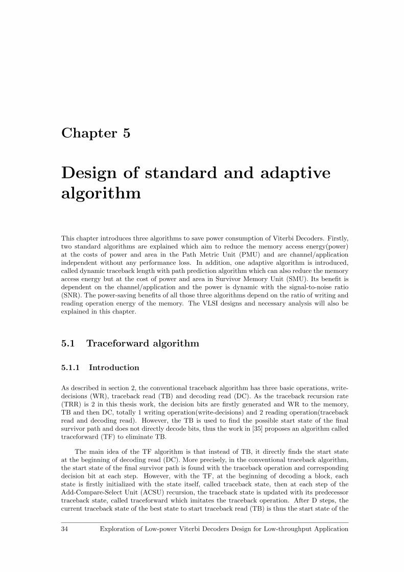
Chapter 5
Design of standard and adaptivealgorithm
This chapter introduces three algorithms to save power consumption of Viterbi Decoders. Firstly,two standard algorithms are explained which aim to reduce the memory access energy(power)at the costs of power and area in the Path Metric Unit (PMU) and are channel/applicationindependent without any performance loss. In addition, one adaptive algorithm is introduced,called dynamic traceback length with path prediction algorithm which can also reduce the memoryaccess energy but at the cost of power and area in Survivor Memory Unit (SMU). Its benefit isdependent on the channel/application and the power is dynamic with the signal-to-noise ratio(SNR). The power-saving benefits of all those three algorithms depend on the ratio of writing andreading operation energy of the memory. The VLSI designs and necessary analysis will also beexplained in this chapter.
5.1 Traceforward algorithm
5.1.1 Introduction
As described in section 2, the conventional traceback algorithm has three basic operations, write-decisions (WR), traceback read (TB) and decoding read (DC). As the traceback recursion rate(TRR) is 2 in this thesis work, the decision bits are firstly generated and WR to the memory,TB and then DC, totally 1 writing operation(write-decisions) and 2 reading operation(tracebackread and decoding read). However, the TB is used to find the possible start state of the finalsurvivor path and does not directly decode bits, thus the work in [35] proposes an algorithm calledtraceforward (TF) to eliminate TB.
The main idea of the TF algorithm is that instead of TB, it directly finds the start stateat the beginning of decoding read (DC). More precisely, in the conventional traceback algorithm,the start state of the final survivor path is found with the traceback operation and correspondingdecision bit at each step. However, with the TF, at the beginning of decoding a block, eachstate is firstly initialized with the state itself, called traceback state, then at each step of theAdd-Compare-Select Unit (ACSU) recursion, the traceback state is updated with its predecessortraceback state, called traceforward which imitates the traceback operation. After D steps, thecurrent traceback state of the best state to start traceback read (TB) is thus the start state of the
34 Exploration of Low-power Viterbi Decoders Design for Low-throughput Application

CHAPTER 5. DESIGN OF STANDARD AND ADAPTIVE ALGORITHM
final survivor path. In such case, the decoding read (DC) can start directly. Define the tracebackstate associated with state i at step n as ui,n. At the beginning of decoding a block, the tracebackstate is initialized with the state itself, so that ui,n=i. Algorithm 3 shows the detail during thewrite-decisions (WR) at step n+k (kD). Once the TF is finished, the decoding read (DC) phasecan start from the us,(n+D), if s is chosen as the best state.
Algorithm 3 Traceforward Algorithm
procedure TF. transfer from state ix to next state xj
for state = 0 to N − 1 douxj,(n+k+1) = uix,(n+k)
Figure 5.1 shows an example of the TF. t1 is the beginning time to decode the bits, so thetraceback state of each state is initialized with the state itself. During the WR from t1 to t6, thetraceback states are updated with its predecessor traceback state during the ACSU recursion. Att6, s1 is selected as the best state to start TB. With conventional traceback, the start state of theDC is found by TB, shown in red array. With the TF, the traceback state of s1 directly indicatesthat the start state of DC is s0, shown in the dashed red array.
Figure 5.1: TF Example
5.1.2 Architecture design
As the TF runs with the generation of decision bits, the design can utilize the structure of the2-way ACSU described in figure 4.5. Figure 5.2(a) shows the new design of the ACSU for theTF and define ux,n as the traceback state of state x at time step n. The rest of design includingthe local and global routing follows the design of the SM. Figure 5.2(b) shows the design of theProcessing Element (PE).
As the traceback recursion rate (TRR) is 2 and single-pointer method is preferred in thisthesis work, the reading speed should be twice as the writing speed to balance the input andoutput of the system. As TB can be eliminated if the TF is applied, the TRR is still 2 whenreading and writing has the same speed. According to the derivation in [3], the memory length is3*D.
Exploration of Low-power Viterbi Decoders Design for Low-throughput Application 35
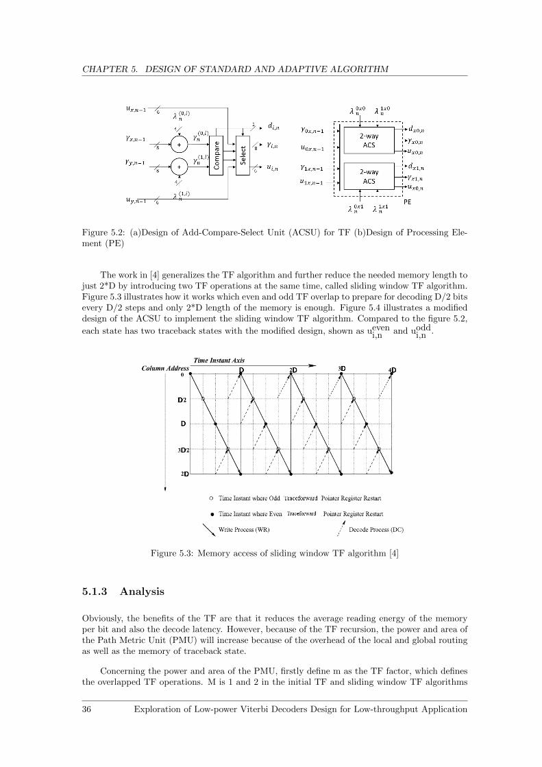
CHAPTER 5. DESIGN OF STANDARD AND ADAPTIVE ALGORITHM
Figure 5.2: (a)Design of Add-Compare-Select Unit (ACSU) for TF (b)Design of Processing Ele-ment (PE)
The work in [4] generalizes the TF algorithm and further reduce the needed memory length tojust 2*D by introducing two TF operations at the same time, called sliding window TF algorithm.Figure 5.3 illustrates how it works which even and odd TF overlap to prepare for decoding D/2 bitsevery D/2 steps and only 2*D length of the memory is enough. Figure 5.4 illustrates a modifieddesign of the ACSU to implement the sliding window TF algorithm. Compared to the figure 5.2,
each state has two traceback states with the modified design, shown as ueveni,n and uodd
i,n .
Figure 5.3: Memory access of sliding window TF algorithm [4]
5.1.3 Analysis
Obviously, the benefits of the TF are that it reduces the average reading energy of the memoryper bit and also the decode latency. However, because of the TF recursion, the power and area ofthe Path Metric Unit (PMU) will increase because of the overhead of the local and global routingas well as the memory of traceback state.
Concerning the power and area of the PMU, firstly define m as the TF factor, which definesthe overlapped TF operations. M is 1 and 2 in the initial TF and sliding window TF algorithms
36 Exploration of Low-power Viterbi Decoders Design for Low-throughput Application
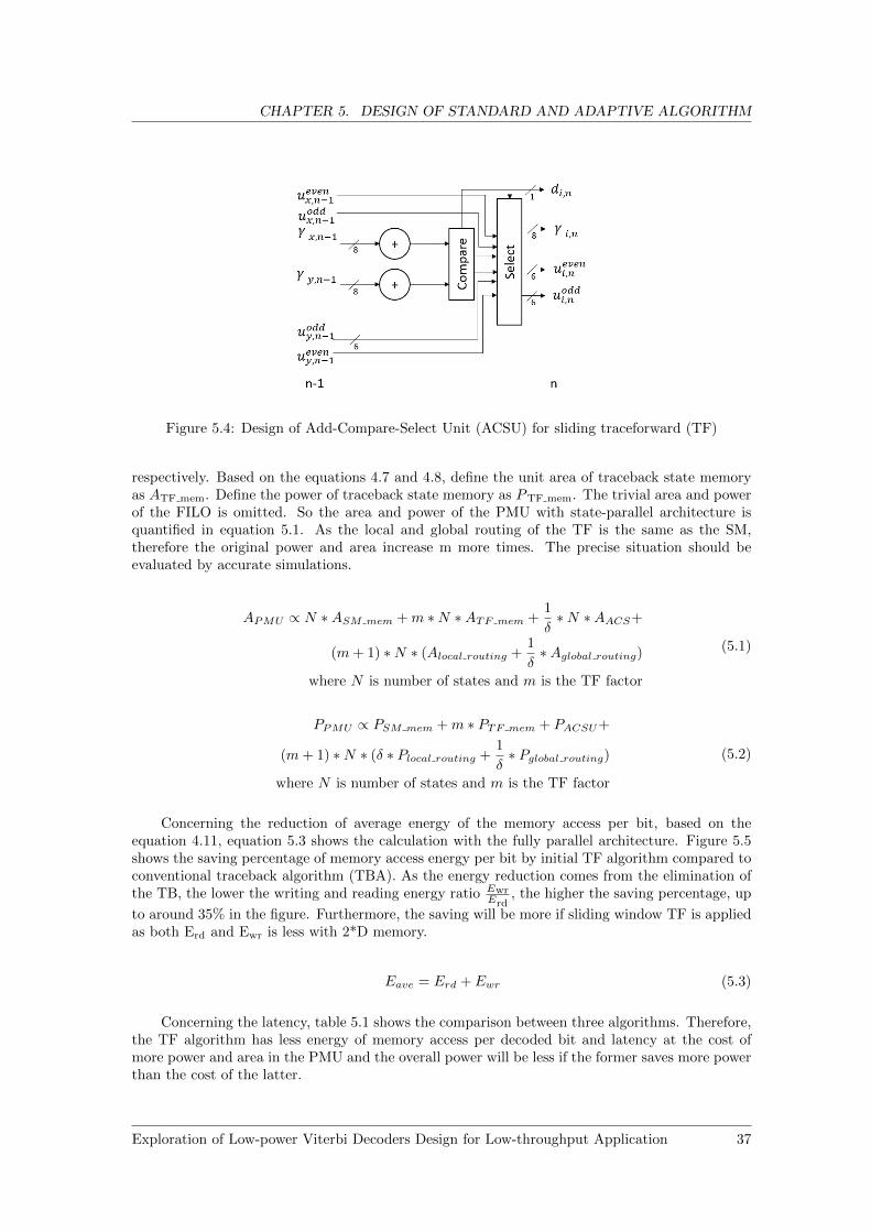
CHAPTER 5. DESIGN OF STANDARD AND ADAPTIVE ALGORITHM
Figure 5.4: Design of Add-Compare-Select Unit (ACSU) for sliding traceforward (TF)
respectively. Based on the equations 4.7 and 4.8, define the unit area of traceback state memoryas ATF mem. Define the power of traceback state memory as PTF mem. The trivial area and powerof the FILO is omitted. So the area and power of the PMU with state-parallel architecture isquantified in equation 5.1. As the local and global routing of the TF is the same as the SM,therefore the original power and area increase m more times. The precise situation should beevaluated by accurate simulations.
APMU ∝ N ∗ASM mem +m ∗N ∗ATF mem +1
δ∗N ∗AACS+
(m+ 1) ∗N ∗ (Alocal routing +1
δ∗Aglobal routing)
where N is number of states and m is the TF factor
(5.1)
PPMU ∝ PSM mem +m ∗ PTF mem + PACSU+
(m+ 1) ∗N ∗ (δ ∗ Plocal routing +1
δ∗ Pglobal routing)
where N is number of states and m is the TF factor
(5.2)
Concerning the reduction of average energy of the memory access per bit, based on theequation 4.11, equation 5.3 shows the calculation with the fully parallel architecture. Figure 5.5shows the saving percentage of memory access energy per bit by initial TF algorithm compared toconventional traceback algorithm (TBA). As the energy reduction comes from the elimination ofthe TB, the lower the writing and reading energy ratio Ewr
Erd, the higher the saving percentage, up
to around 35% in the figure. Furthermore, the saving will be more if sliding window TF is appliedas both Erd and Ewr is less with 2*D memory.
Eave = Erd + Ewr (5.3)
Concerning the latency, table 5.1 shows the comparison between three algorithms. Therefore,the TF algorithm has less energy of memory access per decoded bit and latency at the cost ofmore power and area in the PMU and the overall power will be less if the former saves more powerthan the cost of the latter.
Exploration of Low-power Viterbi Decoders Design for Low-throughput Application 37
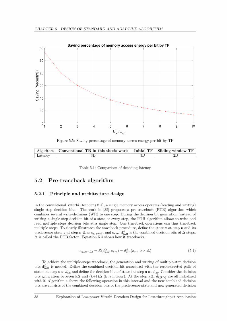
CHAPTER 5. DESIGN OF STANDARD AND ADAPTIVE ALGORITHM
Figure 5.5: Saving percentage of memory access energy per bit by TF
Algorithm Conventional TB in this thesis work Initial TF Sliding window TFLatency 3D 3D 2D
Table 5.1: Comparison of decoding latency
5.2 Pre-traceback algorithm
5.2.1 Principle and architecture design
In the conventional Viterbi Decoder (VD), a single memory access operates (reading and writing)single step decision bits. The work in [35] proposes a pre-traceback (PTB) algorithm whichcombines several write-decisions (WR) to one step. During the decision bit generation, instead ofwriting a single step decision bit of a state at every step, the PTB algorithm allows to write andread multiple steps decision bits at a single step. One traceback operations can thus tracebackmultiple steps. To clearly illustrates the traceback procedure, define the state x at step n and itspredecessor state y at step n-∆ as sy, (n-∆) and sx,n. d∆
x,n is the combined decision bits of ∆ steps.∆ is called the PTB factor. Equation 5.4 shows how it tracebacks.
sy,(n−∆) = Z(d∆x,n, sx,n) = d∆
x,n(sx,n >> ∆) (5.4)
To achieve the multiple-steps traceback, the generation and writing of multiple-step decisionbits d∆
x,n is needed. Define the combined decision bit associated with the reconstructed path of
state i at step n as di,n and define the decision bits of state i at step n as di,n. Consider the decisionbits generation between k∆ and (k+1)∆ (k is integer). At the step k∆, di,(k∆) are all initializedwith 0. Algorithm 4 shows the following operation in this interval and the new combined decisionbits are consists of the combined decision bits of the predecessor state and new generated decision
38 Exploration of Low-power Viterbi Decoders Design for Low-throughput Application
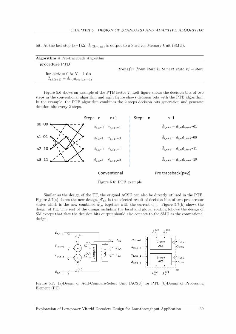
CHAPTER 5. DESIGN OF STANDARD AND ADAPTIVE ALGORITHM
bit. At the last step (k+1)∆, di,((k+1)∆) is output to a Survivor Memory Unit (SMU).
Algorithm 4 Pre-traceback Algorithm
procedure PTB. transfer from state ix to next state xj = state
for state = 0 to N − 1 dodxj,(t+1) = dix,tdstate,(t+1)
Figure 5.6 shows an example of the PTB factor 2. Left figure shows the decision bits of twosteps in the conventional algorithm and right figure shows decision bits with the PTB algorithm.In the example, the PTB algorithm combines the 2 steps decision bits generation and generatedecision bits every 2 steps.
Figure 5.6: PTB example
Similar as the design of the TF, the original ACSU can also be directly utilized in the PTB.Figure 5.7(a) shows the new design. d′i,n is the selected result of decision bits of two predecessorstates which is the new combined di,n together with the current di,n. Figure 5.7(b) shows thedesign of PE. The rest of the design including the local and global routing follows the design ofSM except that that the decision bits output should also connect to the SMU as the conventionaldesign.
Figure 5.7: (a)Design of Add-Compare-Select Unit (ACSU) for PTB (b)Design of ProcessingElement (PE)
Exploration of Low-power Viterbi Decoders Design for Low-throughput Application 39
CHAPTER 5. DESIGN OF STANDARD AND ADAPTIVE ALGORITHM
5.2.2 Analysis
The benefit of the PTB is that it reduces the memory access frequency to ∆ times so that theclock frequency and supply voltage can be reduced to save power. In addition, with the originalclock frequency and supply voltage, the PTB will reduce the energy per decoded bit of the memoryaccess. Specifically, define the overhead energy to write and read a separate bit is Eoverhead whichrelates to the multiplexer and control. Assume that Eoverhead is constant for the same size memoryregardless of its length and word width. The conventional algorithm needs write-decisions (WR),traceback read (TB) and decoding read (DC) to decode a bit, so the overhead energy per decodedbit is 3*Eoverhead. If ∆ bits are accessed once, the average overhead energy per bit is 3
∆*Eoverhead,reducing the total average energy per bit. Equation 5.5 compares the energy per decoded bit ofconventional traceback and the PTB. Obviously, the drawback is the same as the TF, resulting inmore power and area of overhead in the Path Metric Unit (PMU). The total power will be reducedif the saving power is more than the overhead.
Eave = 2 ∗ Erd + Ewr + 3 ∗ EoverheadEave = 2 ∗ Erd + Ewr + (3/∆) ∗ Eoverhead
(5.5)
5.3 Dynamic traceback length with path prediction algorithm
5.3.1 Introduction and architecture design
The work in [17, 6] proposes an adaptive algorithm, called dynamic traceback length algorithm.The main idea of the algorithm is that the survivor depth(traceback length) is usually configuredfor the worst case, 5*K, so that the traceback path can merge to the final survivor path fordecoding, but the decoder does not always work in the worst case. Instead, when the SNR is high,the traceabck path will quickly merge to the final survivor path only after a few steps, thereforethere is a possibility that the current traceback path can re-merge to the previous path. In thatcase, if an extra buffer is applied for the previous path, the memory reading to decode currentblock can be eliminated. The work in [17, 6] proposes an adaptive algorithm, called dynamictraceback length algorithm. The main idea of the algorithm is that the survivor depth(tracebacklength) is usually configured for the worst case, 5*K, so that the traceback path can merge to thefinal survivor path for decoding, but the decoder does not always work in the worst case. Instead,when the SNR is high, the traceabck path will quickly merge to the final survivor path only aftera few steps, therefore there is a possibility that the current traceback path can re-merge to theprevious path. In that case, if an extra buffer is applied for the previous path, the memory readingto decode current block can be eliminated.
Furthermore, the work in [6] also introduces a path prediction algorithm based on the ideathat the best state of each step has higher probability to be in the final survivor path. So duringthe WR operation, the best state of each step is selected by the comparison tree and is added tothe prediction buffer if it is reachable from the previous best state. Figure 5.8 illustrates the ideaof the algorithm. The two dashed red rectangles show the possible traceback path re-merge ofthe current block to the previous block. Appendix C shows the flow chart of two ideas. The pathprediction executes during the WR and dynamic traceback length executes during the TB andDC. For simplicity, the whole algorithm is called dynamic traceback length (DTBL) algorithm.
To implement the DTBL algorithm, an extra buffer is needed for path prediction and bufferingprevious traceback path. To save the buffer size, only decision bits are buffered which calculatesthe buffer state at each step. Figure 5.9 illustrates the design of the SMU for the DTBL algorithm
40 Exploration of Low-power Viterbi Decoders Design for Low-throughput Application

CHAPTER 5. DESIGN OF STANDARD AND ADAPTIVE ALGORITHM
Figure 5.8: Illustration of the DTBL algorithm
and the dashed red rectangle shows the extra component to support the DTBL.
Figure 5.9: Design of Survivor Memory Unit (SMU)
5.3.2 Analysis
As the DTBL only buffers the traceback path from the previous block decoding, there will not existany BER performance compared to the conventional VD which is verified by Matlab simulations.Another significant benefit of the DTBL is that it reduces the memory reading with the buffer,which depends on the level of the SNR. Define the saving percentage as σ which is related to
Exploration of Low-power Viterbi Decoders Design for Low-throughput Application 41

CHAPTER 5. DESIGN OF STANDARD AND ADAPTIVE ALGORITHM
the SNR (EbN0), the equation 5.6 quantifies the energy per bit of memory access based on thefully parallel architecture. Figure 5.10 shows the simulation result to indicate the memory savingpercentage of different SNR in the additive white Gaussian noise (AWGN) channel. It can beobserved that the reduced memory reading percentage can go up to 95% when EbN0=6dB. Also,the total memory access energy per decoded bit of different Ewr/Erd ratio is drawn, up to 65%saving when Ewr/Erd is 1 and EbN0 is 6dB. However, to buffer the previous traceback path andpredict the path, extra components are added, resulting in more power and area. Similar as theprevious algorithms, the general system can consume less power when the benefit exceeds thecosts.
Eave = (1−σ)*2*Erd + Ewr (5.6)
Figure 5.10: Memory access saving with the DTBL algorithm
42 Exploration of Low-power Viterbi Decoders Design for Low-throughput Application

Chapter 6
Implementation, results andanalysis
6.1 Introduction
This chapter describes the implementation of IC designs of three architectures, two standardalgorithms and one adaptive algorithms, which would possibly reduce the power consumption andarea. The architectures contain fully parallel, shared-factor 2 and 4. Those algorithms containtraceforward, pre-traceback and dynamic traceback length and path predication. Furthermore,to fairly compare the area and power, control variate method is applied so that architecturesare all based on the same conventional algorithm and algorithms are implemented with the samearchitecture. The criteria to evaluate the low-power performance of a design is energy/bit whichis the ratio of power and throughput. As the throughput of all the designs are the same, so it isequivalent to evaluate power to indicate the performance. The results from front-end and back-endsimulations including area and power are presented as well as necessary theoretical analysis. Anoptimal implementation is selected at the end concerning the area and power for the applicationcontext of this thesis work.
All designs are implemented firstly by the Verilog to model the behaviour and then is verifiedby the NCsim. Then RTLcompiler is applied for logical front-end synthesis to generate gate-level netlist with the CMOS library as well as estimated area size. With the PrimeTime, coarsepower consumption is obtained. In the front-end simulation, the standard cell-based memoryis substituted temporarily by register files. After evaluating the results, only promising designsare selected for back-end simulations. In the back-end synthesis, Cadence Encounter is applied,including floor-planning, placement, clock tree synthesis, route, post-route optimization and layoutgeneration. Then PrimeTime is applied again to estimate the power with the parasitic extractedfrom the layout.
6.2 Specification
The general specification for the Viterbi Decoder for the 802.11ah standard implemented are
1. K =7(64 states), R=1/2 convolutional decoder,
Exploration of Low-power Viterbi Decoders Design for Low-throughput Application 43

CHAPTER 6. IMPLEMENTATION, RESULTS AND ANALYSIS
2. Generator polynomials, g0=1338 and g1=1718,
3. 4-bit soft decision input log-likelihood ratio (LLR),
4. 4-bit Branch Metric (BM) and 8-bit Path Metric (PM),
5. Best state decoding,
6. Traceback algorithm with survivor depth (traceback length) D=32 and decoding depthM=32,
7. Throughput 5 Mb/s,
8. Dual-port standard cell-based memory (SCM),
9. TSMC CMOS 40nm technology with 1.1V supply voltage.
The other code rate with the punctuation is omitted in this thesis work and only QPSK isconsidered as an example of the modulation scheme when evaluating the BER performance.
6.3 Implementation of different architectures
This section discusses the implementation of three architectures, fully-parallel, shared factor 2 and4 architectures. The idea of designs, front-end and back-end results concerning the power and areaas well as analysis are explained in this section.
6.3.1 Design
Before the implementation, it is important to derive the maximum Processing Element (PE)shared factor by equation 4.9. According to the post timing report generated by the CadenceRTLcompiler, the critical path is the Add-Compare-Select (ACS) operation which is roughly 18000ps and thus the maximum clock frequency is 55Mhz. As the requirement throughput is 5Mb/s,the maximum shared factor is 8 which indicates that 2, 4 and 8 are feasible in this thesis work.Therefore, fully-parallel, shared-factor 2 and 4 are to be implemented to investigate the power andarea performance.
The design of the Branch Metric Unit (BMU) follows the discipline in chapter 4 which applies4-bit uniform quantization scheme for the LLR input. The modular arithmetic normalizationapproach is used in the Add-Compare-Select Unit (ACSU) of the Path Metric Unit (PMU). Thenumber of the PE of the fully parallel, shared-factor 2 and 4 architectures are 32, 16 and 8respectively. The local and global routing as well as the scheduling follows the section 4.3 andappendix D shows the detail configurations. An extra control unit is implemented in the sharedarchitecture to control the local routing of the PE. In addition, a comparison tree module is addedto find the best state for the start of the traceback read (TB).
To implement the Survivor Memory Unit (SMU), as described in section 4.4, the tracebackalgorithm is chosen in this thesis work with the single-pointer reading method and the best statedecoding scheme. As traceback recursion rate (TRR) is 2, the reading speed(traceback read (TB)and decoding read (DC)) should be twice the writing speed. One column represents 64 decisionbits in this thesis work. In the fully parallel architecture, decision-bits of all states are generatedevery cycle and the writing speed is 1 column/cycle. So the reading speed requires 2 columns/cycle.One simple solution to fulfill the required TRR is to generate and write a column of decision bits
44 Exploration of Low-power Viterbi Decoders Design for Low-throughput Application

CHAPTER 6. IMPLEMENTATION, RESULTS AND ANALYSIS
at one cycle and suspend for the next cycle. So the writing speed is 1 column per 2 cycles and asingle reading pointer can achieve 1 column/cycle reading speed which fulfills the required TRR.Based on the work in [3], the memory length is 3*D, so the memory size is 96 length with 64 bisof each column, totally 6 kbits. To achieve a 5Mb/s throughput, the clock frequency should beset as 10 MHz.
In the shared-factor 2 architecture, as two radix-2 trellis shares one PE, it takes 2 cycles(slices) to generate all decision-bits and half column is written per cycle. So the writing speed isthus 1 column per 2 cycles. As the decision bits of slice 0 are from state 0 to 15 and state 32 to 47and the rest decision-bits are from slice 1, so the second most significant bit (MSB) of a tracebackstate determines whether its decision bit is from slice 0 or slice 1. During the traceback read (TB)and decoding read (DC), it only takes one cycle to read the target decision bit for a given state.In such case, the reading speed can be regarded as 1 column/cycle which conforms to the requiredTRR. Therefore the clock frequency is 10 MHz and the memory configuration is 192 length with32 bits of each column.
Similarly, to design the SMU of shared factor 4 architecture, the second and third MSB bitsof the traceback state determine which memory column to be read for its decision bits. So thereading speed can also achieve 1 column/cycle. As the writing are 1 column per 4 cycles, 1 columnper 2 cycles reading speed is sufficient to fulfill the required TRR. The clock frequency is 20 MHzand the memory configuration is 384 length with 16 bits of each column. Table 6.1 lists theconfiguration of clock frequency and memory size of three architectures.
Architecture Clk freq (MHz) Memory sizeFully parallel 10 96× 64 bitsShared factor 2 10 192× 32 bitsShared factor 4 20 384× 16 bits
Table 6.1: Specification of three architectures
6.3.2 Back-end results and analysis
After the implementation, the front-end results are shown in appendix E.1 with necessary ana-lysis. In the back-end synthesis, the standard cell-based memory (SCM) is used and figure 6.1illustrates the comparison of power distributions by the back-end synthesis. The total power ofthe fully-parallel, shared-2 and shared-4 architecture are 247uW, 272uW and 339uW. Similar tosituations by front-end synthesis, the PMU and memory dominates the general power, however,the proportion of PMUs is over half, up to 60% because of the usage of the low-power standardcell-based memory. Figure 6.2 indicates the power distribution of the PE of three architectures.The result are similar to figure E.2, showing that the power of local routing is linear to the sharedfactor and power of all the ACSU is constant. Furthermore, by equation E.1, the power of globalrouting can be calculated and figure 6.3 shows the results with the comparison tree and controlunit. The result is also similar to figure E.3 and it shows that the main difference is the powerof the control unit as higher shared architecture need more complex scheduling. The power oftraceback unit are also nearly the same.
Concerning the memory power, based on the equation 4.11, equation 6.1 shows the theoret-ical power, assuming the energy per cycle of reading and writing is Erd and Ewr and the frequencyof reading and writing is frd and fwr. The calculation results of the power of the fully parallel,shared factor 2 and 4 are 67 uW, 59 uW and 59 uW respectively, which conforms to the ratio ofthe obtained results. Furthermore, the total memory power saving of shared factor 2 and 4 archi-tectures compared to the fully parallel architecture is 12% and 13%. The ratio of the energy/cycle
Exploration of Low-power Viterbi Decoders Design for Low-throughput Application 45
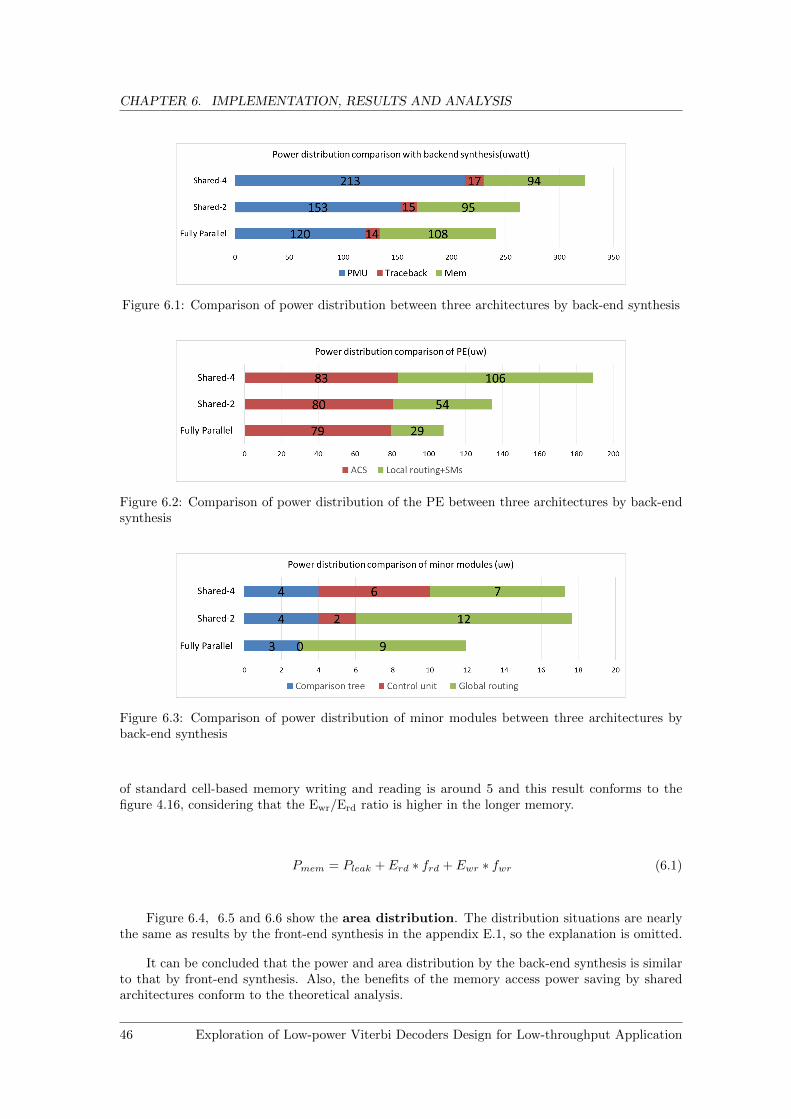
CHAPTER 6. IMPLEMENTATION, RESULTS AND ANALYSIS
Figure 6.1: Comparison of power distribution between three architectures by back-end synthesis
Figure 6.2: Comparison of power distribution of the PE between three architectures by back-endsynthesis
Figure 6.3: Comparison of power distribution of minor modules between three architectures byback-end synthesis
of standard cell-based memory writing and reading is around 5 and this result conforms to thefigure 4.16, considering that the Ewr/Erd ratio is higher in the longer memory.
Pmem = Pleak + Erd ∗ frd + Ewr ∗ fwr (6.1)
Figure 6.4, 6.5 and 6.6 show the area distribution. The distribution situations are nearlythe same as results by the front-end synthesis in the appendix E.1, so the explanation is omitted.
It can be concluded that the power and area distribution by the back-end synthesis is similarto that by front-end synthesis. Also, the benefits of the memory access power saving by sharedarchitectures conform to the theoretical analysis.
46 Exploration of Low-power Viterbi Decoders Design for Low-throughput Application
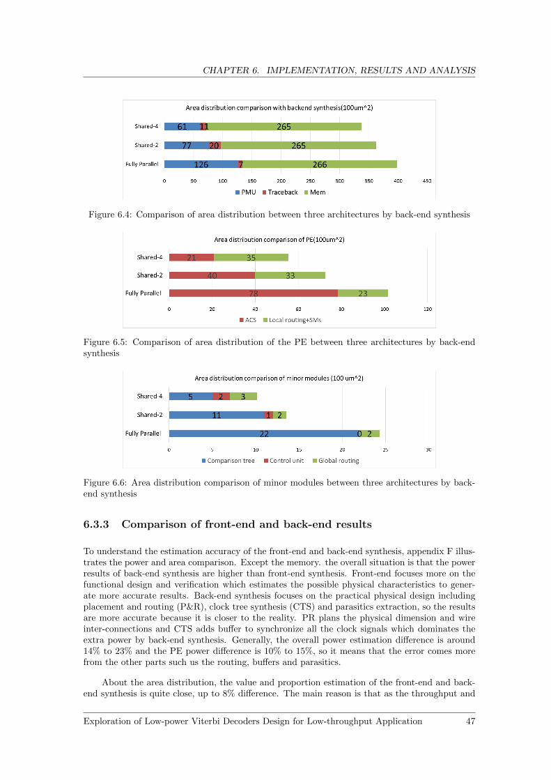
CHAPTER 6. IMPLEMENTATION, RESULTS AND ANALYSIS
Figure 6.4: Comparison of area distribution between three architectures by back-end synthesis
Figure 6.5: Comparison of area distribution of the PE between three architectures by back-endsynthesis
Figure 6.6: Area distribution comparison of minor modules between three architectures by back-end synthesis
6.3.3 Comparison of front-end and back-end results
To understand the estimation accuracy of the front-end and back-end synthesis, appendix F illus-trates the power and area comparison. Except the memory. the overall situation is that the powerresults of back-end synthesis are higher than front-end synthesis. Front-end focuses more on thefunctional design and verification which estimates the possible physical characteristics to gener-ate more accurate results. Back-end synthesis focuses on the practical physical design includingplacement and routing (P&R), clock tree synthesis (CTS) and parasitics extraction, so the resultsare more accurate because it is closer to the reality. PR plans the physical dimension and wireinter-connections and CTS adds buffer to synchronize all the clock signals which dominates theextra power by back-end synthesis. Generally, the overall power estimation difference is around14% to 23% and the PE power difference is 10% to 15%, so it means that the error comes morefrom the other parts such us the routing, buffers and parasitics.
About the area distribution, the value and proportion estimation of the front-end and back-end synthesis is quite close, up to 8% difference. The main reason is that as the throughput and
Exploration of Low-power Viterbi Decoders Design for Low-throughput Application 47
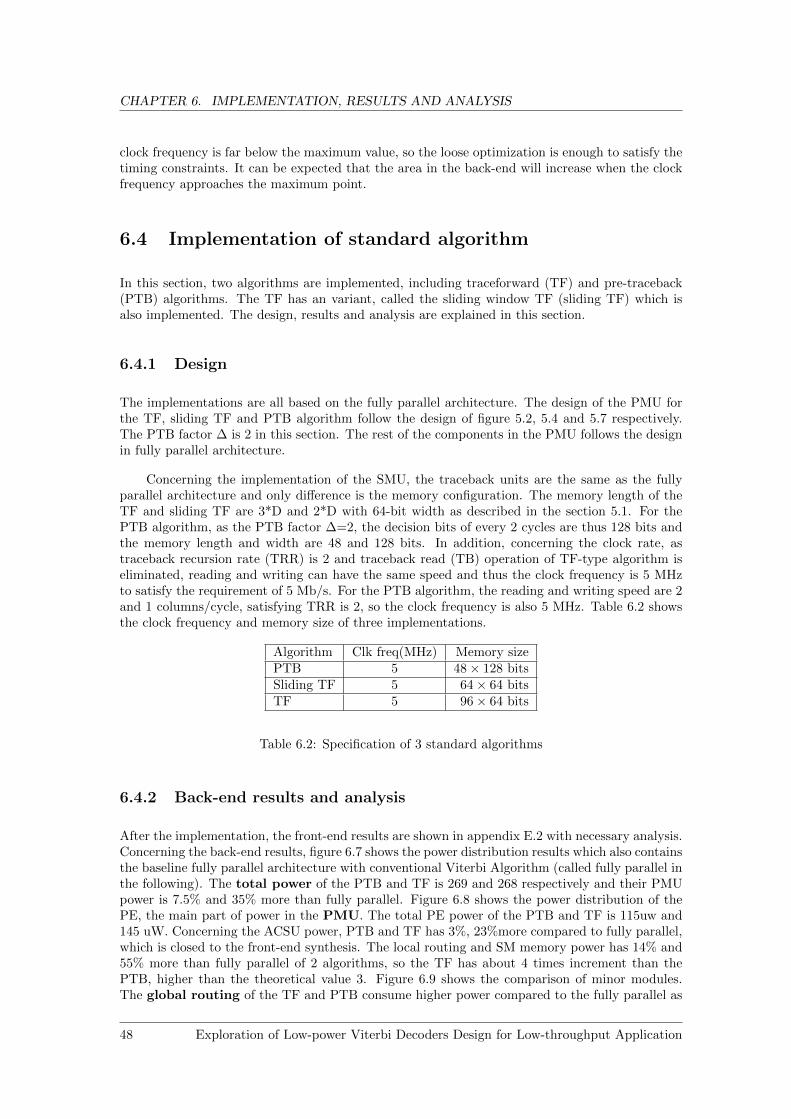
CHAPTER 6. IMPLEMENTATION, RESULTS AND ANALYSIS
clock frequency is far below the maximum value, so the loose optimization is enough to satisfy thetiming constraints. It can be expected that the area in the back-end will increase when the clockfrequency approaches the maximum point.
6.4 Implementation of standard algorithm
In this section, two algorithms are implemented, including traceforward (TF) and pre-traceback(PTB) algorithms. The TF has an variant, called the sliding window TF (sliding TF) which isalso implemented. The design, results and analysis are explained in this section.
6.4.1 Design
The implementations are all based on the fully parallel architecture. The design of the PMU forthe TF, sliding TF and PTB algorithm follow the design of figure 5.2, 5.4 and 5.7 respectively.The PTB factor ∆ is 2 in this section. The rest of the components in the PMU follows the designin fully parallel architecture.
Concerning the implementation of the SMU, the traceback units are the same as the fullyparallel architecture and only difference is the memory configuration. The memory length of theTF and sliding TF are 3*D and 2*D with 64-bit width as described in the section 5.1. For thePTB algorithm, as the PTB factor ∆=2, the decision bits of every 2 cycles are thus 128 bits andthe memory length and width are 48 and 128 bits. In addition, concerning the clock rate, astraceback recursion rate (TRR) is 2 and traceback read (TB) operation of TF-type algorithm iseliminated, reading and writing can have the same speed and thus the clock frequency is 5 MHzto satisfy the requirement of 5 Mb/s. For the PTB algorithm, the reading and writing speed are 2and 1 columns/cycle, satisfying TRR is 2, so the clock frequency is also 5 MHz. Table 6.2 showsthe clock frequency and memory size of three implementations.
Algorithm Clk freq(MHz) Memory sizePTB 5 48× 128 bitsSliding TF 5 64× 64 bitsTF 5 96× 64 bits
Table 6.2: Specification of 3 standard algorithms
6.4.2 Back-end results and analysis
After the implementation, the front-end results are shown in appendix E.2 with necessary analysis.Concerning the back-end results, figure 6.7 shows the power distribution results which also containsthe baseline fully parallel architecture with conventional Viterbi Algorithm (called fully parallel inthe following). The total power of the PTB and TF is 269 and 268 respectively and their PMUpower is 7.5% and 35% more than fully parallel. Figure 6.8 shows the power distribution of thePE, the main part of power in the PMU. The total PE power of the PTB and TF is 115uw and145 uW. Concerning the ACSU power, PTB and TF has 3%, 23%more compared to fully parallel,which is closed to the front-end synthesis. The local routing and SM memory power has 14% and55% more than fully parallel of 2 algorithms, so the TF has about 4 times increment than thePTB, higher than the theoretical value 3. Figure 6.9 shows the comparison of minor modules.The global routing of the TF and PTB consume higher power compared to the fully parallel as
48 Exploration of Low-power Viterbi Decoders Design for Low-throughput Application

CHAPTER 6. IMPLEMENTATION, RESULTS AND ANALYSIS
the interconnection is more complex. Also, the global routing results are all much higher than thefront-end result.
Figure 6.7: Comparison of power distribution between 2 standard algorithms by back-end synthesis
Figure 6.8: Comparison of power distribution of the PE between 2 standard algorithms by back-end synthesis
Figure 6.9: Power distribution comparison of minor modules between 2 standard algorithms byback-end synthesis
To interpret the memory power, equation 6.1 is applied and the result is 60 uW and 58 uWof the PTB and TF. Its ratio is lower than the measured value and also it conforms that theysave power compared to fully parallel. According to the result, the TF saves 15% power whichexactly conforms to the calculation in 5.5 as the ratio of the energy/cycle of standard cell-basedmemory writing and reading is around 5. However, as the overhead in the PMU is larger than thesaving power of memory reading, the overall power of the TF is still higher than the fully parallelarchitecture.
The area distribution of the whole system and the PE are shown in figure 6.10, 6.11and 6.12. Similar to the simulation in section 6.3, the back-end result of area is closed to thefront-end result explained in appendix E.2, so the explanation is omitted.
It can be concluded that the back-end result conforms to the front-end results, which increase20% to 30% of power and around -5% of area. The measured results also correspond to thetheoretical calculation.
Exploration of Low-power Viterbi Decoders Design for Low-throughput Application 49

CHAPTER 6. IMPLEMENTATION, RESULTS AND ANALYSIS
Figure 6.10: Comparison of area distribution between 2 standard algorithms by back-end synthesis
Figure 6.11: Comparison of area distribution of the PE between 2 standard algorithms by back-endsynthesis
Figure 6.12: Area distribution comparison of minor modules between 2 standard algorithms byback-end synthesis
6.4.3 Comparison of front-end and back-end results
The front-end and back-end results are also compared in this section, shown in appendix G. Similarto the situation in section 6.3, because of routing, buffers and parasitics in back-end process, thereexists a difference between the front-end and back-end results and the overall power estimationdifference go up to 20% to 30% of 2 standard algorithms, bigger than previous three architectures.This is because the 2 standard algorithms, especially the TF has much more global routing.
About the area distribution, the proportion of each part is the same between front-end andback-end simulations but the front-end overestimate the overall area with around -5% difference.However, the PE area distribution is closed, showing that the over estimation comes from theglobal routing.
Therefore, comparing the front-end and back-end results, the tool will have more error in thepower estimation and overestimate the area when there is more global routing.
50 Exploration of Low-power Viterbi Decoders Design for Low-throughput Application

CHAPTER 6. IMPLEMENTATION, RESULTS AND ANALYSIS
6.5 Implementation of adaptive algorithm
This section introduces the implementation of dynamic traceback length with path predictionalgorithm. The design, front-end and back-end simulation results and analysis compared to shared-2 architecture are also explained in this section.
6.5.1 Design
The implementation of the dynamic traceback length (DTBL) algorithm are based on the sharefactor 2(called shared-2) architecture so the design of the PMU is the same. The design of theSMU follows the figure 5.9 and the clock frequency is 5MHz to achieve 5Mb/s throughput. Thememory size is also the same as shared-2 architecture, 192× 32 bits.
6.5.2 Back-end results and analysis
After the implementation, the front-end results are shown in appendix E.3 with necessary analysis.The power distribution of back-end results are shown in figure 6.13 which also contains the baselineshared-2 architecture with conventional Viterbi Algorithm (called shared-2 architecture directly inthe following). The PMU power is similar as the shared-2 architecture because the designs are thesame. For the power of the traceback unit, the DTBL consumes 38 uW and 58 uW at 0 dB and6 dB. Figure 6.14 illustrates the power distribution of minor modules. As the comparison treepower is 10 uW and 26 uW, the buffer control power is around 17 uW and 22 uW respectively.The reason is that higher SNR result in more calculation about the traceback path buffer andprediction.
Figure 6.13: Comparison of power distribution between the DTBL and shared-2 by back-endsynthesis
Figure 6.14: Power distribution of minor modules between the DTBL and shared-2 by back-endsynthesis
Concerning the memory power, figure 6.15 shows the memory access power saving based onshared-2 architectures with different ratio of Ewr/Erd. In this thesis work, Ewr/Erd=5, thus the
Exploration of Low-power Viterbi Decoders Design for Low-throughput Application 51

CHAPTER 6. IMPLEMENTATION, RESULTS AND ANALYSIS
power saving goes from 8% at 0 dB to 16% at 6 dB. The measured result shows that memory powersaving 8.4% and 21% which exactly conforms to the theoretical result. Therefore, at EbN0=0 dB,the DTBL saves 7 uW power of memory reading at the cost of 23 uW extra power of the tracebackunit, at EbN=6 dB, the DTBL saves 20 uW power of memory reading at the cost of 43 uW extrapower.
Figure 6.15: Memory access saving with DTB algorithm based on shared-2 architecture
Figure 6.16 shows that the extra area is 1800 um2 of the traceback unit. Appendix Hcompares the front-end and back-end results and situation is almost the same as 6.3.3. Thedifference of power at front-end and back-end simulations is around 15% while the area estimationis almost the same. Detail is not discussed here.
Figure 6.16: Comparison of area distribution of the PE between the DTBL and shared-2 byback-end synthesis
It can be concluded that with the standard cell-based memory, the DTBL cannot save powerat such context because of the cost of the comparison tree and buffer control.
6.6 Comparison of all implementations
To summarize all the implementations concerning the power and area, table 6.3 show the compar-ison by the back-end synthesis compared to the baseline architecture. The ACSU and local routing
52 Exploration of Low-power Viterbi Decoders Design for Low-throughput Application

CHAPTER 6. IMPLEMENTATION, RESULTS AND ANALYSIS
and SM memory are the main components of the PMU. As power is the first priority, among thethree architectures, fully-parallel implementation is the optimal. Although shared architecturecan save up to 15% area, the increment power is up to 37% because of the local routing and SMmemory. It can be expected that shared factor 8 architecture consumes more power with less areawhich does not fit the power requirement.
Comparing the PTB and TF, the PTB is the optimal, as it has the same power with only4% area overhead, compared to 13% overhead of TF. The main extra power of PTB comes fromthe memory and local routing and SM memory which are also the source of extra area. TheTF eliminates the traceback read (TB) operations, resulting in less power at traceback unit andmemory and more area at the PMU especially the local routing and SM memory, around 134%.
The DTBL algorithm does save the power consumption of memory, up to 21% compared toshared-2 architecture and only 5% extra area. However, it consumes up to 267% more powerin the traceback unit. It can be concluded that this implementation can not be applied to savepower. Possible solution is that reduce the power of comparison tree which is the main part ofoverhead. Concerning the PTB, TF and DTBL, as the Ewr/Erd ratio is around 5 in the standardcell-based memory, its benefit of power saving is thus not obvious and the possible solution is toapply different memories with lower Ewr and Ewr/Erd ratio.
Table 6.3: Comparison of all the implementations by back-end synthesis
Table 6.4 illustrates the standard and maximum clock frequency as well as memory size of allthe back-end implementations. Among all the designs, the fully parallel architecture with theconventional Viterbi Algorithms is selected as the optimal design, which consumes least power.Although the PTB consumes a little bit more power compared to fully-parallel architecture, itcan achieve the maximum throughput (40 Mb/s) among all designs with 40 MHz clock rate. Soit is promising to be the optimal low-power design by the voltage and clock rate scaling and itis thus selected as another optimal algorithm among all implemented algorithms. Furthermore,figure 6.17 compares the energy per bit between nominal and maximum clock frequency by back-
Exploration of Low-power Viterbi Decoders Design for Low-throughput Application 53

CHAPTER 6. IMPLEMENTATION, RESULTS AND ANALYSIS
end simulations. Obvious, all the energy per bit decrease when frequency increases because theutilization ratio of clock cycle is higher. Among all the measured data, the conventional fullyparallel architecture and the PTB are optimal.
Furthermore, to compare the front-end and back-end synthesis, the difference of the powerestimation in this thesis work is 10% to 30% while the difference of area estimation is only around5%. Also, based on the results, the influence of the global routing of different designs to powerand area can be omitted.
Table 6.4: Comparison of all the clock frequency and memory size
Figure 6.17: Comparison of energy per bit with maximum clock frequency
54 Exploration of Low-power Viterbi Decoders Design for Low-throughput Application

Chapter 7
Conclusion and recommendations
7.1 Conclusion
This thesis work presents an investigation to design and implement low-power and small-area ICof Viterbi Decoders for low-throughput applications and 802.11ah standard with TSMC 40nmtechnology. The idea is to separately investigate different architectures and different algorithmsto reduce power and area based on the mathematical analysis and literature study. Simulationresults show that the implementation of the fully-parallel architecture with the conventional ViterbiAlgorithm, 247 uW and 0.04 mm2, and the pre-traceback (PTB) algorithm,269 uW and 0.04 mm2,are the optimal designs among all the work. With 1.1V voltage supply, the clock rate is respectively10 MHz and 5 MHz to both achieve a 5 Mb/s throughput. Compared to the power target (200to 400 uW) in the section 2.3, two selected optimal implementations achieve the goal, shown infigure 7.1.
Figure 7.1: Final result
The main contributions of this thesis work are in the following
Exploration of Low-power Viterbi Decoders Design for Low-throughput Application 55
CHAPTER 7. CONCLUSION AND RECOMMENDATIONS
1. Investigate the related algorithm in the literature to reduce power and area for the applicationcontext in this thesis work and quantify a detail target,
2. Build up a simulation chain to evaluate the BER, power and area performance by Matlaband Cadence tools,
3. Propose and implement IC solutions for each components of low-power and small-areadesigns,
4. Design and implement 3 architectures and 3 algorithms to reduce power and area,
5. Compare and investigate the simulation accuracy of Cadence front-end and back-end syn-thesis concerning the are and power,
6. Evaluate and analyze the power and area as well as BER performance by Matlab simulationand Cadence tools. Among all the designs, the fully parallel architecture and pre-traceback(PTB) algorithms are the optimal implementation with the least power and acceptable area.
7.2 Recommendations
Further research work for possible improvements is listed are the following
1. Continue investigate the work in [36, 47, 38] about scarce-state-transition(STT) and T-algorithm to reduce the power of the Path Metric Unit (PMU) at the cost of extra area andBER performance loss.
2. Reduce the power of the bottleneck part of implemented designs. For example, the com-parison tree is the power bottleneck of the dynamic traceback length (DTBL) algorithm,scarce-state-transition algorithm can be applied to find the best state at each step whichconsumes less power.
3. Combine frequency and voltage scaling to further reduce the power of optimal designs whilesatisfying the throughput requirement because the supply voltage of the standard cell-basedmemory can be reduced down to 0.2V which will lead to a tremendous power saving.
56 Exploration of Low-power Viterbi Decoders Design for Low-throughput Application

Bibliography
[1] Keshab K Parhi and Takao Nishitami. Digital Signal processing for multimedia systems,Chapter 17. CRC press, 1999. viivii, 8, 17
[2] Peter J Black and Teresa H Meng. A 140-mb/s, 32-state, radix-4 viterbi decoder. IEEEJournal of solid-state circuits, 27(12):1877–1885, 1992. viivii, 8, 9, 22, 23, 24, 29, 32
[3] Robert Cypher and C Bernard Shung. Generalized trace-back techniques for survivor memorymanagement in the viterbi algorithm. Journal of VLSI signal processing systems for signal,image and video technology, 5(1):85–94, 1993. viivii, 9, 28, 29, 30, 32, 35, 45
[4] Yao Gang, Ahmet T Erdogan, and Tughrul Arslan. An efficient pre-traceback architecturefor the viterbi decoder targeting wireless communication applications. IEEE Transactions onCircuits and Systems I: Regular Papers, 53(9):1918–1927, 2006. viivii, 36
[5] R. Sramek. The on-line Viterbi algorithm. Master’s thesis, Bratislava, 2007. viiiviii, 61
[6] Chien-Ching Lin, Yen-Hsu Shih, Hsie-Chia Chang, and Chen-Yi Lee. Design of a power-reduction viterbi decoder for wlan applications. IEEE Transactions on Circuits and SystemsI: Regular Papers, 52(6):1148–1156, 2005. viiiviii, 8, 10, 40, 63
[7] IEEE Std. IEEE P802.11ah/D5.0. Part 11: Wireless LAN Medium Access Control (MAC)and Physical Layer (PHY) Specifications. 2015. 2, 6
[8] Weiping Sun, Munhwan Choi, and Sunghyun Choi. Ieee 802.11 ah: A long range 802.11 wlanat sub 1 ghz. Journal of ICT Standardization, 1(1):83–108, 2013. 2
[9] Giuseppe Caire, Giorgio Taricco, and Ezio Biglieri. Bit-interleaved coded modulation. In-formation Theory, IEEE Transactions on, 44(3):927–946, 1998. 2, 13
[10] IEEE Std. IEEE P802.11-REVmc/D4.0. Part 11: Wireless LAN Medium Access Control(MAC) and Physical Layer (PHY) Specifications. 2015. 3
[11] Tobias Gemmeke, Michael Gansen, and Tobias G Noll. Implementation of scalable powerand area efficient high-throughput viterbi decoders. IEEE Journal of Solid-State Circuits,37(7):941–948, 2002. 7
[12] Alfred K Yeung and JM Rabaey. A 210 mb/s radix-4 bit-level pipelined viterbi decoder. InSolid-State Circuits Conference, 1995. Digest of Technical Papers. 41st ISSCC, 1995 IEEEInternational, pages 88–89. IEEE, 1995. 8
[13] Peter J Black and TH-Y Meng. A 1-gb/s, four-state, sliding block viterbi decoder. IEEEJournal of Solid-State Circuits, 32(6):797–805, 1997. 8
[14] Inyup Kang and Alan N Willson. Low-power viterbi decoder for cdma mobile terminals.IEEE journal of solid-state circuits, 33(3):473–482, 1998. 8, 9, 24
Exploration of Low-power Viterbi Decoders Design for Low-throughput Application 57
BIBLIOGRAPHY
[15] Hiroshi Suzuki, Yun-Nan Chang, and Keshab K Parhi. Low-power bit-serial viterbi decoderfor next generation wide-band cdma systems. In Acoustics, Speech, and Signal Processing,1999. Proceedings., 1999 IEEE International Conference on, volume 4, pages 1913–1916.IEEE, 1999. 8
[16] Xun Liu and Marios C Papaefthymiou. Design of a high-throughput low-power is95 viterbidecoder. In Proceedings of the 39th annual Design Automation Conference, pages 263–268.ACM, 2002. 8
[17] Chien-Ching Lin, Chia-Cho Wu, and Chen-Yi Lee. A low power and high speed viterbidecoder chip for wlan applications. In Solid-State Circuits Conference, 2003. ESSCIRC’03.Proceedings of the 29th European, pages 723–726. IEEE, 2003. 8, 40
[18] Jie Jin and Chi-Ying Tsui. A low power viterbi decoder implementation using scarce statetransition and path pruning scheme for high throughput wireless applications. In ISLPED’06Proceedings of the 2006 International Symposium on Low Power Electronics and Design,pages 406–411. IEEE, 2006. 8
[19] Fei Sun and Tong Zhang. Low power state-parallel relaxed adaptive viterbi decoder designand implementation. In 2006 IEEE International Symposium on Circuits and Systems, pages4–pp. IEEE, 2006. 8
[20] Koushik Maharatna, Alfonso Troya, Milos Krstic, and Eckhard Grass. On the implementationof a low-power ieee 802.11 a compliant viterbi decoder. In 19th International Conference onVLSI Design held jointly with 5th International Conference on Embedded Systems Design(VLSID’06), pages 6–pp. IEEE, 2006. 8
[21] Fei Sun and Tong Zhang. Low-power state-parallel relaxed adaptive viterbi decoder. IEEETransactions on Circuits and Systems I: Regular Papers, 54(5):1060–1068, 2007. 8
[22] Jie Jin and Chi-ying Tsui. Low-power limited-search parallel state viterbi decoder implement-ation based on scarce state transition. IEEE Transactions on Very Large Scale Integration(VLSI) Systems, 15(10):1172–1176, 2007. 8
[23] C Arun and V Rajamani. A low power and high speed viterbi decoder based on deep pipelined,clock blocking and hazards filtering. International Journal of Communications, Network andSystem Sciences, 2(6):575, 2009. 8
[24] Xin-Ru Lee, Hsie-Chia Chang, and Chen-Yi Lee. A low-power radix-4 viterbi decoder basedon dcvspg pulsed latch with sharing technique. In Circuits and Systems (APCCAS), 2010IEEE Asia Pacific Conference on, pages 1203–1206. IEEE, 2010. 8
[25] Woong Choi, Gyuseong Kang, and Jongsun Park. A refresh-less edram macro with embeddedvoltage reference and selective read for an area and power efficient viterbi decoder. IEEEJournal of Solid-State Circuits, 50(10):2451–2462, 2015. 8
[26] T Gemmeke, VS Gierenz, and TG Noll. Scalable, power and area efficient high throughputviterbi decoder implementations. In Solid-State Circuits Conference, 2001. ESSCIRC 2001.Proceedings of the 27th European, pages 474–477. IEEE, 2001. 8
[27] Irfan Habib, Ozgun Paker, and Sergei Sawitzki. Design space exploration of hard-decisionviterbi decoding: algorithm and vlsi implementation. IEEE transactions on very large scaleintegration (VLSI) systems, 18(5):794–807, 2010. 8, 10, 21
[28] Ivan M Onyszchuk, K-M Cheung, and Oliver Collins. Quantization loss in convolutionaldecoding. IEEE transactions on communications, 41(2):261–265, 1993. 8, 19, 20
58 Exploration of Low-power Viterbi Decoders Design for Low-throughput Application
BIBLIOGRAPHY
[29] Filippo Tosato and Paola Bisaglia. Simplified soft-output demapper for binary interleavedcofdm with application to hiperlan/2. In Communications, 2002. ICC 2002. IEEE Interna-tional Conference on, volume 2, pages 664–668. IEEE, 2002. 8, 14
[30] Herbert Dawid, Gerhard Fettweis, and Heinrich Meyr. A cmos ic for gb/s viterbi decoding:System design and vlsi implementation. IEEE Transactions on Very Large Scale Integration(VLSI) Systems, 4(1):17–31, 1996. 9, 24
[31] C Bernard Shung, H-D Lin, Robert Cypher, Paul H Siegel, and Hemant K Thapar. Area-efficient architectures for the viterbi algorithm. i. theory. IEEE transactions on communica-tions, 41(4):636–644, 1993. 9, 26
[32] Montserrat Boo, Francisco Arguello, Javier D Bruguera, Ramon Doallo, and Emilio L Za-pata. High-performance vlsi architecture for the viterbi algorithm. IEEE transactions oncommunications, 45(2):168–176, 1997. 9, 23, 25, 26
[33] C Bernard Shung, Paul H Siegel, Gottfried Ungerboeck, and Hemant K Thapar. Vlsi archi-tectures for metric normalization in the viterbi algorithm. In Communications, 1990. ICC’90,Including Supercomm Technical Sessions. SUPERCOMM/ICC’90. Conference Record., IEEEInternational Conference on, pages 1723–1728. IEEE, 1990. 9, 22, 23
[34] G David Forney Jr. The viterbi algorithm. Proceedings of the IEEE, 61(3):268–278, 1973. 9,13, 28, 29
[35] Peter J Black and TH-Y Meng. Hybrid survivor path architectures for viterbi decoders.In Acoustics, Speech, and Signal Processing, 1993. ICASSP-93., 1993 IEEE InternationalConference on, volume 1, pages 433–436. IEEE, 1993. 9, 34, 38
[36] Ming-Hwa Chan, Wen-Ta Lee, Mao-Chao Lin, and Liang-Gee Chen. Ic design of an adaptiveviterbi decoder. IEEE Transactions on Consumer Electronics, 42(1):52–62, 1996. 9, 56
[37] Emmanuel Boutillon and Luis Gonzalez. Trace back techniques adapted to the survivingmemory management in the m algorithm. In Acoustics, Speech, and Signal Processing, 2000.ICASSP’00. Proceedings. 2000 IEEE International Conference on, volume 6, pages 3366–3369. IEEE, 2000. 9
[38] Tsunehachi Ishitani, Kazuo Tansho, Norio Miyahara, Shuji Kubota, and Shuzo Kato. Ascarce-state-transition viterbi-decoder vlsi for bit error correction. IEEE journal of solid-state circuits, 22(4):575–582, 1987. 10, 56
[39] Jan Stuyt. Standard cell-based memory for low voltage operation. Technical Report TN-12-WATS-TP1-073, Holst Centre, High Tech Campus, Eindhoven, September 2012. 10, 32
[40] Andrew J Viterbi. Error bounds for convolutional codes and an asymptotically optimumdecoding algorithm. Information Theory, IEEE Transactions on, 13(2):260–269, 1967. 13
[41] Ephraim Zehavi. 8-psk trellis codes for a rayleigh channel. Communications, IEEE Transac-tions on, 40(5):873–884, 1992. 13
[42] Andrew J Viterbi. An intuitive justification and a simplified implementation of the mapdecoder for convolutional codes. Selected Areas in Communications, IEEE Journal on,16(2):260–264, 1998. 14
[43] Ivan M Onyszchuk. Truncation length for viterbi decoding. IEEE Transactions on Commu-nications, 39(7):1023–1026, 1991. 16, 17
[44] Robert J McEliece and Ivan M Onyszchuk. Truncation effects in viterbi decoding. 1989. 16,17
Exploration of Low-power Viterbi Decoders Design for Low-throughput Application 59

BIBLIOGRAPHY
[45] Llr vs. hard decision demodulation. http://nl.mathworks.com/help/comm/examples/
llr-vs-hard-decision-demodulation-1.html. Accessed: 22-06-2016. 17
[46] Andries P Hekstra. An alternative to metric rescaling in viterbi decoders. IEEE Transactionson Communications, 37(11):1220–1222, 1989. 22
[47] Shuji Kubota, Shuzo Kato, and Tsunehachi Ishitani. Novel viterbi decoder vlsi implement-ation and its performance. IEEE Transactions on Communications, 41(8):1170–1178, 1993.56
60 Exploration of Low-power Viterbi Decoders Design for Low-throughput Application
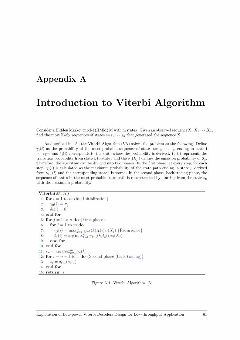
Appendix A
Introduction to Viterbi Algorithm
Consider a Hidden Markov model (HMM) M with m states. Given an observed sequence X=X1,· · · ,Xn,find the most likely sequences of states s=s1,· · · ,sn that generated the sequence X.
As described in [5], the Viterbi Algorithm (VA) solves the problem as the following. Defineγj(i) as the probability of the most probable sequence of states s=s1,· · · ,sj-1, ending in state ii.e. sj=i and δj(i) corresponds to the state where the probability is derived. tk (i) represents thetransition probability from state k to state i and the ei (Xj ) defines the emission probability of Xj.Therefore, the algorithm can be divided into two phases. In the first phase, at every step, for eachstep, γj(i) is calculated as the maximum probability of the state path ending in state j, derivedfrom γj-1(i) and the corresponding state i is stored. In the second phase, back-tracing phase, thesequence of states in the most probable state path is reconstructed by starting from the state sn
with the maximum probability.
Figure A.1: Viterbi Algorithm [5]
Exploration of Low-power Viterbi Decoders Design for Low-throughput Application 61

Appendix B
Conventional Viterbi Algorithm
Algorithm 5 Conventional VD algorithm
Require: rec signal, trunc legnth1: procedure VD2: block length← LENGTH(rec signal)/N . N is 2, NO. of output3: path memory ← int[NO ST ∗ trunc legnth] . NO ST is 64, NO. of states4: l← 05: sum metric[] ← 0
6: for l ++ < block length do . evolve all trellis, PMU7: rec bit0← rec signal[l*N]8: rec bit1← rec signal[l*N+1]9: s← 0
10: temp sum metric[] ← 011: for s++ < NO ST do12: branch state0 = Prev state(s, 0)13: branch state1 = Prev state(s, 1)14: zero metric, one metric = BMU(s,rec bit0,rec bit1,branch state0,branch state1)15: temp zero metric← sum metric[s]+zero metric16: temp one metric← sum metric[s]+zero metric17: if temp zero metric < temp one metric then18: temp sum metric[s]← temp zero metric19: path memory[s*block length]← 020: else21: temp sum metric[s]← temp one metric22: path memory[s*block length]← 1
23: sum metric[]← temp sum metric[]24:
25: min metric state = MIN(sum metric) . traceback from min metric, SMU26: t← l − 127: for t-- > l - trunc legnth do28: min metric state = Prev state(min metric state, path memory[min metric state]
29: dec bits[t] = get input(min metric state) . decode last state
30:
31: return dec bits
62 Exploration of Low-power Viterbi Decoders Design for Low-throughput Application

Appendix C
Flow chart of dynamic truncationlength and path predictionalgorithm
This appendix illustrates the flow chart of dynamic truncation length and path prediction al-gorithm.
Figure C.1: Illustration of (a) dynamic truncation length (b)path prediction algorithm [6]
Exploration of Low-power Viterbi Decoders Design for Low-throughput Application 63

Appendix D
Routing of fully parallel, sharedfactor 2 and 4
This appendix shows the global and local routing configuration of three different architectures.Table D.1 shows the scheduler in the local routing of PMU for shared factor 2 and 4. The index0, 1 and shift control wire corresponds to the interface in figure 4.9 (a).
Table D.1: Scheduler in the local routing of PMU for (a) shared factor 2 and (b) shared factor 4
Table D.2 and D.3 illustrate the global routing table for fully-parallel, shared factor 2 and 4architectures. The nomination of pex in/out y indicates the connection of input/output port y ofprocessing element(PE) x.
64 Exploration of Low-power Viterbi Decoders Design for Low-throughput Application

APPENDIX D. ROUTING OF FULLY PARALLEL, SHARED FACTOR 2 AND 4
Table D.2: Global routing table of fully parallel architecture
Table D.3: Global routing table of (a) shared factor 2 and (b) shared factor 4
Exploration of Low-power Viterbi Decoders Design for Low-throughput Application 65

Appendix E
Analysis of the front-endsimulation results
This appendix compares and analyzes the front-end simulation results of all the implementations.
E.1 Front-end results and analysis of three architectures
Figure E.1 shows the comparison of the power distribution between those three architectures.The total power of the fully-parallel, shared-2 and shared-4 architecture are 156uW, 230uW and413uW. The PMU and memory consumes around half of the total power, dominating the overallconsumption which conforms to the power distribution in several literature. Concerning the PMU,figure E.2 shows the detail power distribution. The SM memory in the fully parallel architectureaccounts for most of the power of the sum power of the local routing and SM memory. So thepower of the local routing of shared-2 and shared-4 architectures can be calculated by subtractingit and results are 31uW and 71uW. The ratio of the result, 0.43, closed to the theoretical value 0.5of equation 4.8 indicating that the power of local routing linearly scales with the shared factor.
Figure E.1: Comparison of power distribution between three architectures by front-end synthesis
Concerning the power of the global routing, equation 4.8 shows it is inverse proportional tothe shared factor δ. The power of the global routing Pglobal routing can be calculated by subtractingthe power of the PE PPE, control units and other sub-modules Pminor modules from the PMUPPMU, shown in equation E.1. Figure E.3 shows calculation results as well as the power of thecontrol unit and comparison tree. As the power of the global routing is closed and tiny for threearchitectures, the global routing power can be omitted in such situation. Furthermore, the powerof the control unit increases with higher shared factor, as the SM memory needs more complex
66 Exploration of Low-power Viterbi Decoders Design for Low-throughput Application
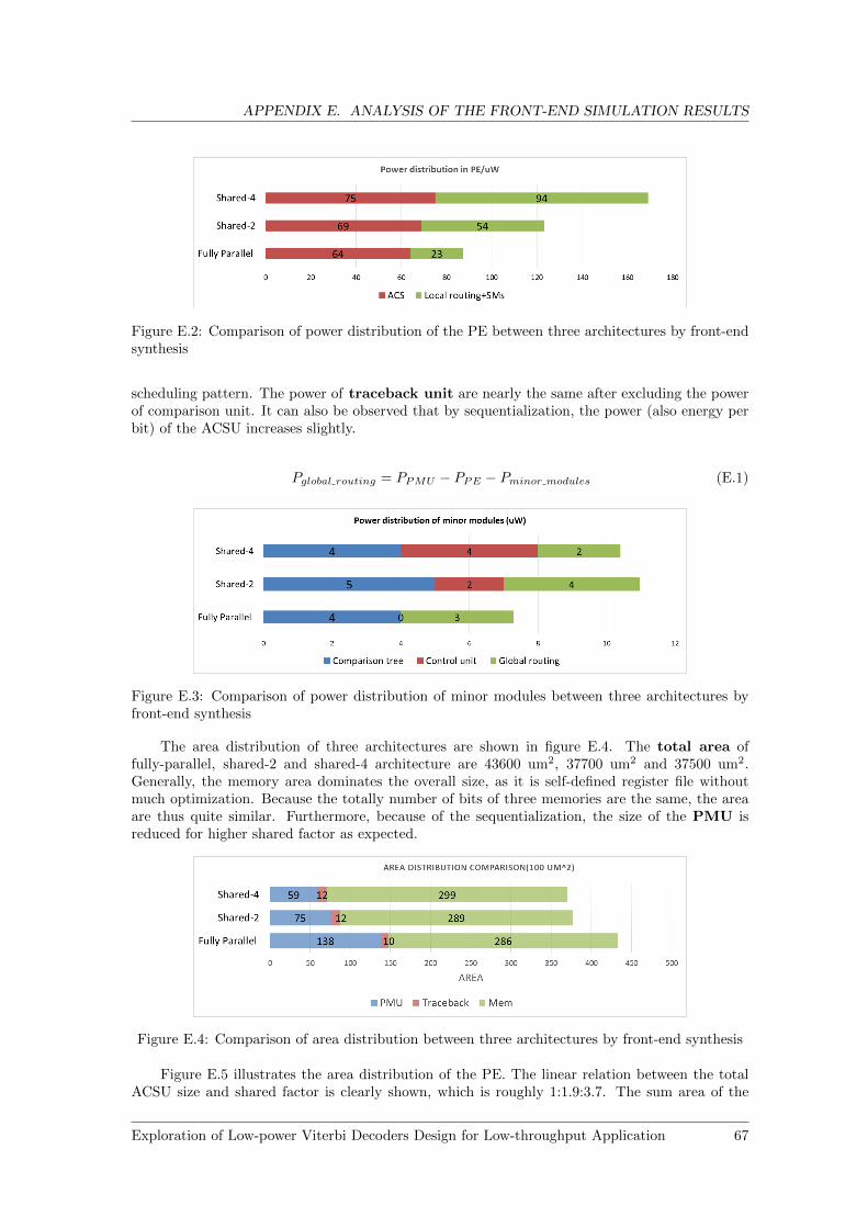
APPENDIX E. ANALYSIS OF THE FRONT-END SIMULATION RESULTS
Figure E.2: Comparison of power distribution of the PE between three architectures by front-endsynthesis
scheduling pattern. The power of traceback unit are nearly the same after excluding the powerof comparison unit. It can also be observed that by sequentialization, the power (also energy perbit) of the ACSU increases slightly.
Pglobal routing = PPMU − PPE − Pminor modules (E.1)
Figure E.3: Comparison of power distribution of minor modules between three architectures byfront-end synthesis
The area distribution of three architectures are shown in figure E.4. The total area offully-parallel, shared-2 and shared-4 architecture are 43600 um2, 37700 um2 and 37500 um2.Generally, the memory area dominates the overall size, as it is self-defined register file withoutmuch optimization. Because the totally number of bits of three memories are the same, the areaare thus quite similar. Furthermore, because of the sequentialization, the size of the PMU isreduced for higher shared factor as expected.
Figure E.4: Comparison of area distribution between three architectures by front-end synthesis
Figure E.5 illustrates the area distribution of the PE. The linear relation between the totalACSU size and shared factor is clearly shown, which is roughly 1:1.9:3.7. The sum area of the
Exploration of Low-power Viterbi Decoders Design for Low-throughput Application 67

APPENDIX E. ANALYSIS OF THE FRONT-END SIMULATION RESULTS
local routing and SM memory in the fully parallel architecture are dominated by the SM memory.As the total memory of the SM are the same for different architectures, the local routing area ofshared architectures can be calculated by subtracting the area of the SM memory. The calculationresults of shared 2 and 4 are similar and this result conforms to the equation 4.7 indicating thatthe area of total local routing is constant for shared architecture.
Figure E.5: Comparison of area distribution of the PE between three architectures by front-endsynthesis
For the area of global routing Aglobal routing, it can be obtained by subtracting the area ofthe PE APE, control units and other sub-modules Aminor modules from the PMU APMU, shown inequation E.2. The results are shown in figure E.6 with the comparison tree and control unit. Thecalculation results of the global routing is trivial, so its area can be omitted in front-end synthesis.Concerning the area of the comparison tree, the ratio of the fully parallel, shared factor 2 and4 is about 4:2:1. The reason is that the comparison tree computes the a column of the SM of onecycle, so its size is linear to the number of PE. So the theoretical ratio of the comparison tree areais 4:2:1 which explains the result.
Aglobal routing = APMU −APE −Aminor modules (E.2)
Figure E.6: Comparison of area distribution of minor modules between three architectures byfront-end synthesis
Therefore, based on the simulation results of front-end synthesis, concerning the PMU, it canbe concluded that the shared architecture has less area at the cost of more power. The extrapower comes from the local routing which is linear to the shared factor. Also, both the power andarea of the global routing can be omitted. However, the benefit of area is less significant when theshared factor increases because of the existence of the SM memory and local routing area.
68 Exploration of Low-power Viterbi Decoders Design for Low-throughput Application

APPENDIX E. ANALYSIS OF THE FRONT-END SIMULATION RESULTS
E.2 Front-end results and analysis of two standard algorithms
Figure E.7 illustrates the comparison of power distribution between 3 standard algorithms as wellas a conventional VD with fully parallel architecture(called fully parallel in the following). Thetotal power of the PTB, sliding TF and TF are 145 uW, 200 uW and 179 uW and their PMUpower is 11%, 63% and 38% more than fully parallel architecture. Figure E.8 shows the detailpower distribution of the PE, compared with fully parallel.
Figure E.7: Comparison of power distribution between 2 standard algorithms by front-end syn-thesis
Figure E.8: Comparison of power distribution of the PE between 2 standard algorithms by front-end synthesis
Concerning the ACSU power, PTB, TF and sliding TF has 6%, 23% and 30% more comparedto fully parallel, which are the overhead in the ACSU. Concerning the local routing and SM memorypower, which is mainly SM memory, the three algorithms has 26%, 74% and 157% more. Thereason is that the PTB only needs 2*2 more bits memory of each the PE for ∆=2 while the TFand sliding TF need 2*6 and 2*2*6 more bits(each traceback state has 6 bits). So theoreticallybased on the power modelling of equation 5.1, the extra power of the SM memory in the TF andsliding TF shall be 3 and 6 times more than the PTB, which conforms to the practical value 2.8and 6.
Furthermore, by equation E.1, the power of the global routing can be calculated and fig-ure E.9 shows the results with the comparison tree and control unit. The results are all around4 uw, indicating that the extra power can be omitted for the three algorithms. As the tracebackfrequency of sliding TF algorithm is twice the other algorithms, its comparison tree consumesmore power to generate the best state to start the traceback.
Concerning the power of the memory, the results are 51, 32, 44 and 41 of the fully parallel,PTB, TF and sliding TF respectively. Equation 5.5 explains why PTB has less memory power thanfully parallel, as it has less overhead. In addition, according to equation 5.3, TF-type algorithms
Exploration of Low-power Viterbi Decoders Design for Low-throughput Application 69

APPENDIX E. ANALYSIS OF THE FRONT-END SIMULATION RESULTS
Figure E.9: Power distribution comparison of minor modules between 2 standard algorithms byfront-end synthesis
reduce one reading operation of each decoded bit, therefore it has less power consumption. Assliding TF only needs 2*D memory compared to TF, it consumes less power, 41 uW.
The area distribution of three algorithms compared to the fully parallel architecture areshown in figure E.10. The total memory size is 45400 um2, 47600 um2 and 42800 um2of thePTB, sliding TF and TF respectively. The memory area of the PTB and TF are the same as theyhave the same number of bits while sliding TF has around 2
3 proportion memory area.
Figure E.10: Comparison of area distribution between 2 standard algorithms by front-end synthesis
Concerning the area of the PMU, figure E.11 illustrates the area distribution of the PE.Compared to fully parallel, the ACSU of the PTB, TF and sliding TF has 1%, 9% and 17%more area, which is the overhead area. The SM memory has 38%, 129% and 225% more area,so TF and sliding TF has 3.3 and 5.9 times than the PTB, conforming to the equation 5.1, asthe extra area scales linearly with the memory size. Also, figure E.12 shows the global routingsize, which is 200, 600 and 600 um2 of the PTB, TF and sliding TF. As the TF-type needs widerinterconnections, it has more area of global routing. However, as it only accounts for 1% of thetotal area, the influence can be omitted.
Therefore, based on the front-end simulation results, all three algorithms have less powerconsumption of the memory at the costs of more area and power in PMUs. Similar to the simulationof different architectures in the previous section, the power and area of global routing can also beomitted. In addition, the PTB is the optimal design concerning the power with a slight more areacompared to fully parallel design. Although the sliding TF has smallest aera, the power is thehighest, more than 38% compared to the PTB. Thus it is not necessary to continue the back-endsimulation for the sliding TF.
70 Exploration of Low-power Viterbi Decoders Design for Low-throughput Application
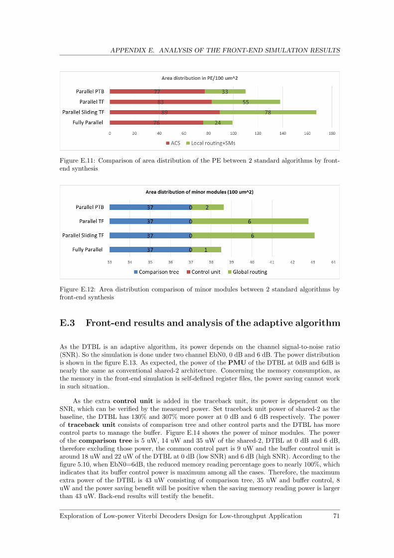
APPENDIX E. ANALYSIS OF THE FRONT-END SIMULATION RESULTS
Figure E.11: Comparison of area distribution of the PE between 2 standard algorithms by front-end synthesis
Figure E.12: Area distribution comparison of minor modules between 2 standard algorithms byfront-end synthesis
E.3 Front-end results and analysis of the adaptive algorithm
As the DTBL is an adaptive algorithm, its power depends on the channel signal-to-noise ratio(SNR). So the simulation is done under two channel EbN0, 0 dB and 6 dB. The power distributionis shown in the figure E.13. As expected, the power of the PMU of the DTBL at 0dB and 6dB isnearly the same as conventional shared-2 architecture. Concerning the memory consumption, asthe memory in the front-end simulation is self-defined register files, the power saving cannot workin such situation.
As the extra control unit is added in the traceback unit, its power is dependent on theSNR, which can be verified by the measured power. Set traceback unit power of shared-2 as thebaseline, the DTBL has 130% and 307% more power at 0 dB and 6 dB respectively. The powerof traceback unit consists of comparison tree and other control parts and the DTBL has morecontrol parts to manage the buffer. Figure E.14 shows the power of minor modules. The powerof the comparison tree is 5 uW, 14 uW and 35 uW of the shared-2, DTBL at 0 dB and 6 dB,therefore excluding those power, the common control part is 9 uW and the buffer control unit isaround 18 uW and 22 uW of the DTBL at 0 dB (low SNR) and 6 dB (high SNR). According to thefigure 5.10, when EbN0=6dB, the reduced memory reading percentage goes to nearly 100%, whichindicates that its buffer control power is maximum among all the cases. Therefore, the maximumextra power of the DTBL is 43 uW consisting of comparison tree, 35 uW and buffer control, 8uW and the power saving benefit will be positive when the saving memory reading power is largerthan 43 uW. Back-end results will testify the benefit.
Exploration of Low-power Viterbi Decoders Design for Low-throughput Application 71
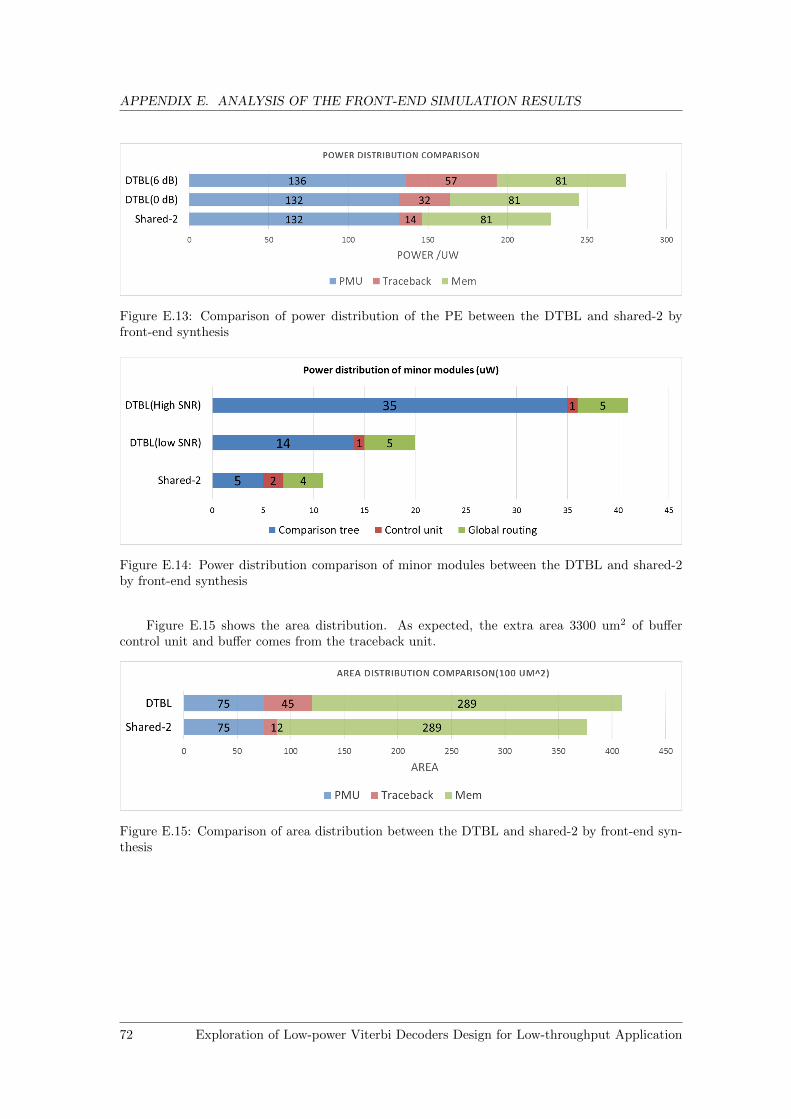
APPENDIX E. ANALYSIS OF THE FRONT-END SIMULATION RESULTS
Figure E.13: Comparison of power distribution of the PE between the DTBL and shared-2 byfront-end synthesis
Figure E.14: Power distribution comparison of minor modules between the DTBL and shared-2by front-end synthesis
Figure E.15 shows the area distribution. As expected, the extra area 3300 um2 of buffercontrol unit and buffer comes from the traceback unit.
Figure E.15: Comparison of area distribution between the DTBL and shared-2 by front-end syn-thesis
72 Exploration of Low-power Viterbi Decoders Design for Low-throughput Application

Appendix F
Comparison of results by thefront-end and back-end synthesisof different architectures
This appendix compares the power and area distribution of fully-parallel, shared factor 2 and 4architectures from the front-end and back-end simulations.
Figure F.1: Comparison of power distribution with front-end and back-end synthesis
Exploration of Low-power Viterbi Decoders Design for Low-throughput Application 73

APPENDIX F. COMPARISON OF RESULTS BY THE FRONT-END AND BACK-ENDSYNTHESIS OF DIFFERENT ARCHITECTURES
Figure F.2: Comparison of power distribution of PEs with front-end and back-end synthesis
Figure F.3: Comparison of area distribution with front-end and back-end synthesis
Figure F.4: Comparison of area distribution of PEs with front-end and back-end synthesis
74 Exploration of Low-power Viterbi Decoders Design for Low-throughput Application
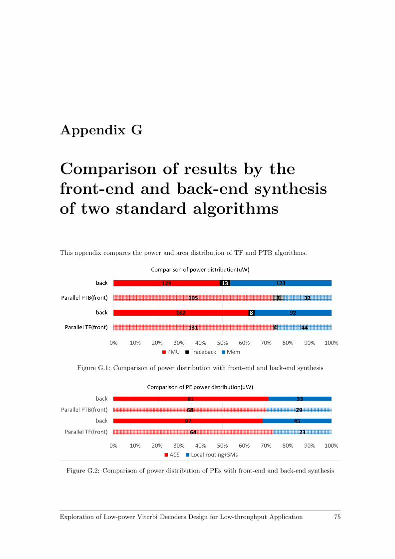
Appendix G
Comparison of results by thefront-end and back-end synthesisof two standard algorithms
This appendix compares the power and area distribution of TF and PTB algorithms.
Figure G.1: Comparison of power distribution with front-end and back-end synthesis
Figure G.2: Comparison of power distribution of PEs with front-end and back-end synthesis
Exploration of Low-power Viterbi Decoders Design for Low-throughput Application 75

APPENDIX G. COMPARISON OF RESULTS BY THE FRONT-END AND BACK-ENDSYNTHESIS OF TWO STANDARD ALGORITHMS
Figure G.3: Comparison of area distribution with front-end and back-end synthesis
Figure G.4: Comparison of area distribution of PEs with front-end and back-end synthesis
76 Exploration of Low-power Viterbi Decoders Design for Low-throughput Application
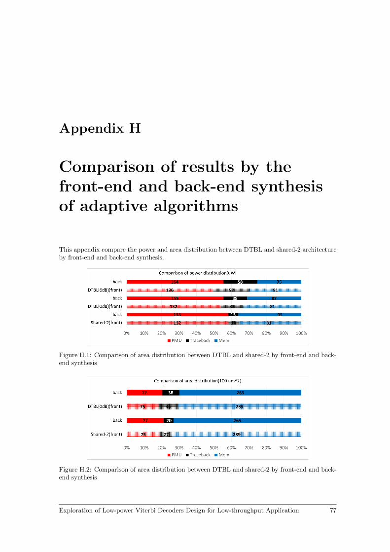
Appendix H
Comparison of results by thefront-end and back-end synthesisof adaptive algorithms
This appendix compare the power and area distribution between DTBL and shared-2 architectureby front-end and back-end synthesis.
Figure H.1: Comparison of area distribution between DTBL and shared-2 by front-end and back-end synthesis
Figure H.2: Comparison of area distribution between DTBL and shared-2 by front-end and back-end synthesis
Exploration of Low-power Viterbi Decoders Design for Low-throughput Application 77