Embed Size (px)
Citation preview
Eindhoven University of Technology
MASTER
Wavelength conversion by using a 1550 nm laser amplifier
Muhammad Chaidar Chairuddin Lakare, C.
Award date:1999
DisclaimerThis document contains a student thesis (bachelor's or master's), as authored by a student at Eindhoven University of Technology. Studenttheses are made available in the TU/e repository upon obtaining the required degree. The grade received is not published on the documentas presented in the repository. The required complexity or quality of research of student theses may vary by program, and the requiredminimum study period may vary in duration.
General rightsCopyright and moral rights for the publications made accessible in the public portal are retained by the authors and/or other copyright ownersand it is a condition of accessing publications that users recognise and abide by the legal requirements associated with these rights.
• Users may download and print one copy of any publication from the public portal for the purpose of private study or research. • You may not further distribute the material or use it for any profit-making activity or commercial gain
Take down policyIf you believe that this document breaches copyright please contact us providing details, and we will remove access to the work immediatelyand investigate your claim.
Download date: 29. May. 2018
EINDHOVEN UNIVERSITY OF TECHNOLOGYDEPARTMENT OF ELECTRICAL ENGINEERING
Division of Telecommunication Technologiesand Electromagnetism
Wavelength Conversionby Using a 1550 nm Laser Amplifier
M.C.C. Lakare
Master's thesisJanuary 1999 - September 1999Eindhoven
Supervisors:
Prof. ir. G.D. KhoeDr. ir. H. de Waardt
The department of Electrical Engineering of the Eindhoven University of Technology is notresponsible for the contents of trainee reports and graduate reports
CHAPTER 1 3
INTRODUCTION 3
CHAPTER2 6
SEMICONDUCTOR OPTICAL AMPLIFIERS 6
2.1 INTRODUCTION 62.2 SEMICONDUCTOR OPTICAL AMPLIFIERS 72.3 PROGRESS AND ApPLICATIONS 92.4 IMpORTANT CRITERIA OF TWA SEMICONDUCTOR OPTICAL AMPLIFIERS 10
CHAPTER 3 11
WAVELENGTH CONVERSION 11
CHAPTER 4 16
CROSS GAIN MODULATION 16
4.1 INTRODUCTION 164.2 THEORY AND MODEL 18
4.2.1 Basic Equations 194.2.2 Scattering Losses 20
4.3 TRANSMISSION FUNCTION 224.3.1 Definitions and Assumptions 224.3.2 THE LARGE-SIGNAL ANALYSIS 244.3.3 THE SMALL-SIGNAL ANALySIS 254.3.4 Gain Model 26
4.4 EXTINCTION RATIO (ER) AND SIGNAL-TO-NOISERATIO (SNR) 284.5 DYNAMIC RESPONSE 31
CHAPTER 5 34
MEASUREMENT AND SIMULATION 34
5.1 STATIC MEASUREMENT 355.1.1 Quadratic Fitting the Unsaturated Gain 385.1.2. Fitting the differential gain 38
5.2 DYNAMIC MEASUREMENT 405.2.1 Extinction Ratio (ER) 415.2.2 Bit Error Rate 43
5.3 SIMULATION 495.3.1 Scattering losses 495.3.2 Simulation ofGain Dynamic 505.3.3 Simulation ofwaveform 52
CHAPTER 6 54
CONCLUSIONS AND RECOMMENDATIONS 54
MEASUREMENT; 54SIMULATION: 55
ACKNOWLEDGMENTS 56
APPENDIX A.1 57
APPENDIX A.2 58
APPENDIX A.3 61
APPENDIX B.l 63
APENDIX B.2 67
APPENDIX C 69
APPENDIX D 70
APPENDIX E 71
APPENDIX F 72
APPENDIX G 73
APPENDIX H 75
APPENDIX I 76
BIBLIOGRAPHY 77
2
Chapter 1
Introduction
The function of wavelength conversion (WC) will become very important for wavelength-division multiplexed systems (WDM). In WDM networks, a connection must beestablished along a route by using a common wavelength on all of the links along theroute. This constraint may be removed by the introduction of wavelength converters,which are devices which take the data modulated on an input wavelength and transfer itto a different output wavelength (in wavelength domain), thus improving the networkblocking performance.
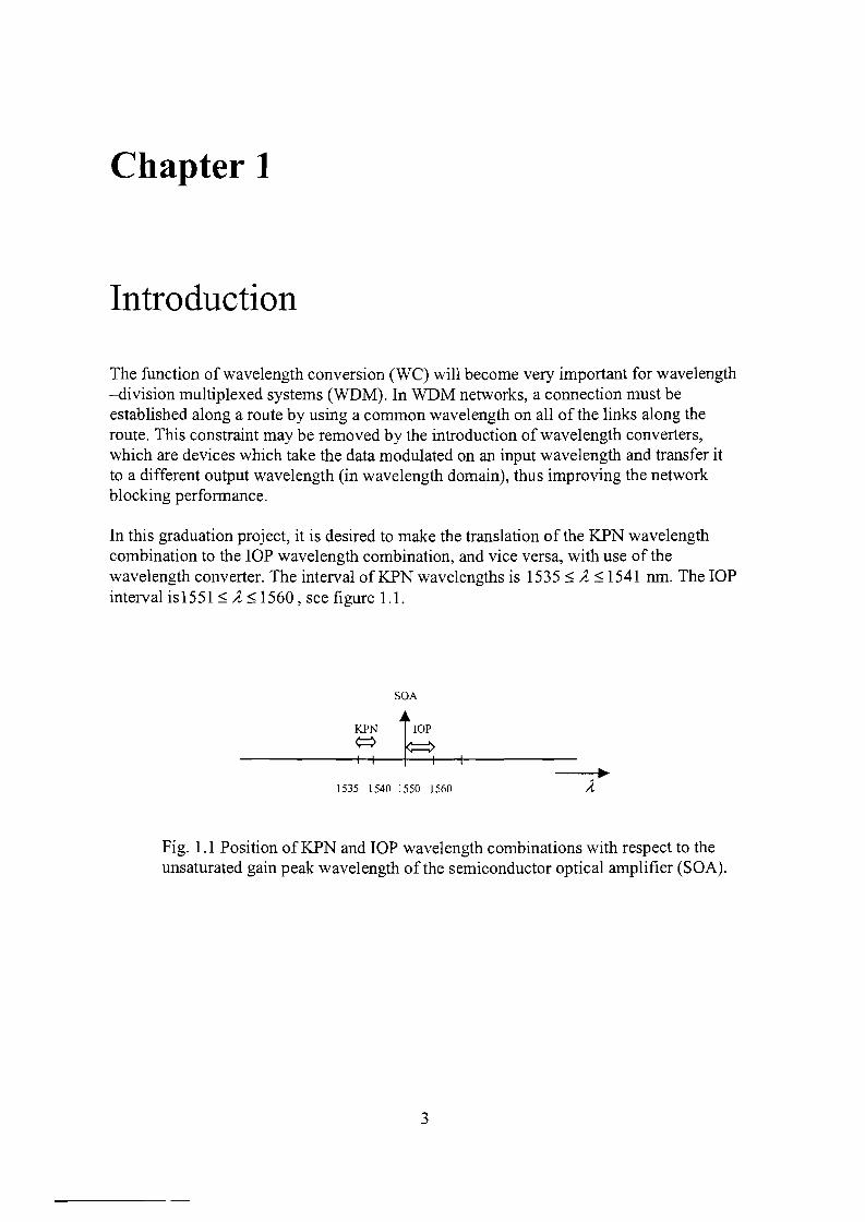
In this graduation project, it is desired to make the translation of the KPN wavelengthcombination to the lOP wavelength combination, and vice versa, with use of thewavelength converter. The interval ofKPN wavelengths is 1535 ~ A ~ 1541 nm. The lOPinterval is 1551 ~ A ~ 1560 , see figure 1.1.
SOA
~~------II-+I-~--+-------1535 1540 1550 1560
Fig. 1.1 Position ofKPN and lOP wavelength combinations with respect to theunsaturated gain peak wavelength of the semiconductor optical amplifier (SOA).
3
The table of the wavelength range are also given below
No. lOP channel (D.A = 3.20 nm) KPN channel (D.A = ~0.8 nm)1 1551.00 1535.82
12 1554.20 1536.593 1557.40 1537.394 1560.60 1538.185 ----- 1538.976 ----- 1539.747 ----- 1540.53
Wavelength converters have been demonstrated based a wide variety of mechanisms,such as optoelectronic (O/E), cross-gain modulation (XGM), cross-phase modulation(XPM), four-wave mixing (FWM) and etc.
Because the conversion must be easy in implementation, it was decided to apply theXGM converter. The reason are 1) it doesn't require optical filter at the probe output tofilter away the input data signal, 2) higher conversion efficiency and 3) lower powerlevels. This converter uses the nonlinearity characteristic of semiconductor opticalamplifiers (SOA).
The purpose of this report is establishing the detailed knowledge system performance ofcross-gain modulation wavelength conversion based on 1550 nm semiconductor opticalamplifier (SOA). With this knowledge, the translation vfboth the interval wavelengthbetween KPN and lOP would be studied. Because the distance between these twointervals is too long, the conversion should be done 1) from 1551 nm down to 1540.53nm (down conversion) and 2) from 1540.53 nm up to 1551 nm (up conversion). Thefollowing aspects had to be adressed during the research in general
o wavelength dependence;o power dependence; input power requirements for pump and the probe signals,o polarization dependence,o extinction ratio (ER),o signal-to-noise ratios (SNR),o conversion efficiency; the ratio of the converted signal to the input signal,o pulse form conservation and propagation effects.
to arrive at the optimal conditions when a translation must be done from one intervalwavelength to another interval. The most important task is to define the range of thewavelength conversion based on the SOA with the ER as a criterium.
4

The organization of this report as follows:
The introduction in chapter one describes motivation and the choice made for this finalproject. A basic knowledge about semiconductor optical amplifiers must be firstintroduced and will be given in chapter two. After that, a general description ofwavelength conversion is given with different techniques and components and it is givenin chapter three. The realization of the wavelength conversion is done withsemiconductor optical amplifier as the key component. Based on the choice of thetechnique that has been made, the cross-gain modulation and with all its systemperformance is presented in chapter four. Chapter five gives a comparison of thesimulation and the measurement results. The conclusions and recommendations are givenin chapter six. Last but not least, additional information is also given in a number ofappendixes.
5
Chapter 2
Semiconductor Optical Amplifiers
2. J Introduction
Optical Amplifiers are conventionally used in trunk transmission lines, optical subscribernetworks and virtually all communication systems. They not only provide simplecompensation for the losses produced in optical circuits, but also have a tremendousimpact on the field of optical functional devices, for instance, optical switches and signalprocessors.
The fiber-optic optic communications, which makes use of the low loss, broadbandcharacteristics of optical fibers and the advantages of having light as a carrier, isprogressing at a drastic pace. The wavelength division multiplexing (WDM) has beenconsidered as a promissing technology to increase the flexibility and capacity of opticalnetworks. Furthermore, by utilizing functionalities such as all-optical wavelengthconversion and TDM-to-WDM translation the network throughput can be greatlyenhanced.
Semiconductor optical amplifiers (SOAs) or semiconductor laser amplifiers (SLAs) areattractive devices for amplification of a number of multiplexed channels simultaneouslyand for wavelength conversion in a WDM network.Compared with EDFA's, SOAs have a potential advantage ofbeing integrated with otherdevices in the same substrate and have a strong nonlinearity, which is essential for signalprocessmg.
In this chapter, a brief explanation of semiconductor optical amplifiers (SOAs) is given.
All optical wavelength conversion will become an essential function in wavelengthdivision multiplexed networks and photonic switch blocks. This block can be providedusing semiconductor optical amplifier (SOA's). The purpose in this chapter is to providebasic knowledge of the semiconductor optical amplifier that can be exploited later forwavelength conversion
6
2.2 Semiconductor Optical Amplifiers
The investigation into optical amplification firstly began in the mid-1960's with the oscillation ofarare-earth glass laser. Back into the 1980s, initially, narrow band Fabry-Perot amplifiers (FPAs)were studied. Following this, as resonance mode frequency ripples were suppressed by reducing thefacet reflectivity, broadband optical amplifiers in the form of travelling wave amplifiers (TWAs)were realized.
If a bias current is applied to a semiconductor laser just below its oscillation threshold, the devicewill act as an optical amplifier. Since the modal gain is lower than the intemalloss of the laser, thedevice does not reach the oscillation, but incident light is amplified on the basis of the modal gain.In this case, although the amplification is enlarged by the resonance, it requires a critical frequencymatching between the input signal and the FP resonant mode. Resonance also causes gainsaturation which deteriorates the amplifier performance. Therefore, it is primarily an essential stepto reduce the cavity resonance.
Semiconductor optical amplifier (SOA) can be divided into two groups.If the input optical signal comes through the one side ofthe laser resonator and amplified opticalsignal leaves the resonator through the other side of the resonator, then the amplifier is consideredto be of transmission type (travelling type and with a sufficiently low facet reflectivity) and mostoften considered in the literature as Travelling-Wave Amplifier (TWA). The TWA canprovide 25-30 dB optical gain over a bandwidth of 40-80 TIm. The reflectivity of both facets can besuppressed, such as by
precise antireflection (AR) coating [2],angled (or tilted) facet and [3,5]window facet [4]
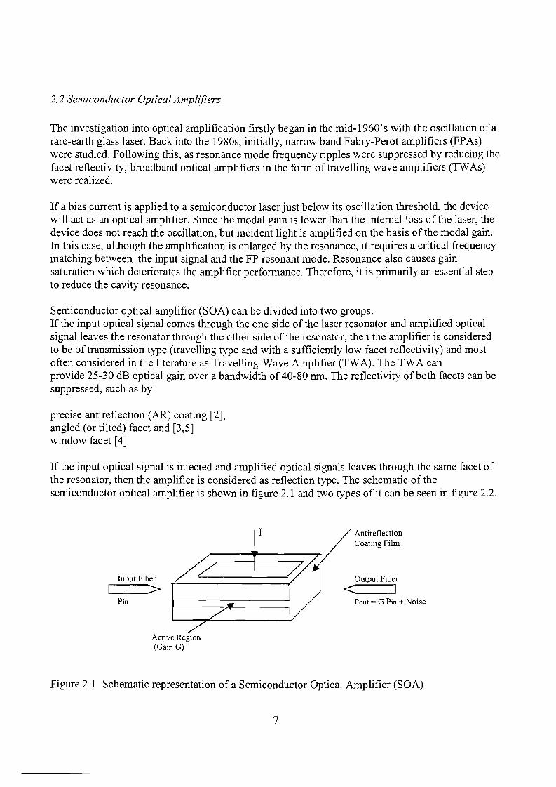
If the input optical signal is injected and amplified optical signals leaves through the same facet ofthe resonator, then the amplifier is considered as reflection type. The schematic of thesemiconductor optical amplifier is shown in figure 2.1 and two types of it can be seen in figure 2.2.
Input Fiber
'----->Pin
I AntireflectionCoating Film
Output Fiber
< IPout = G Pin + Noise
Active Region(Gain G)
Figure 2.1 Schematic representation of a Semiconductor Optical Amplifier (SOA)
7
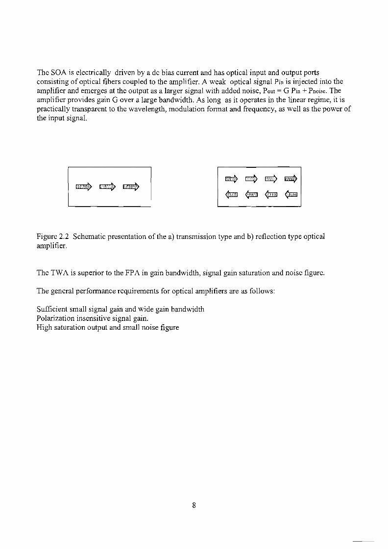
The SOA is electrically driven by a dc bias current and has optical input and output portsconsisting of optical fibers coupled to the amplifier. A weak optical signal Pin is injected into theamplifier and emerges at the output as a larger signal with added noise, Pout = G Pin + Pnoise. Theamplifier provides gain G over a large bandwidth. As long as it operates in the linear regime, it ispractically transparent to the wavelength, modulation format and frequency, as well as the power ofthe input signal.
~E4~
~~¢E8
Figure 2.2 Schematic presentation of the a) transmission type and b) reflection type opticalamplifier.
The TWA is superior to the FPA in gain bandwidth, signal gain saturation and noise figure.
The general performance requirements for optical amplifiers are as follows:
Sufficient small signal gain and wide gain bandwidthPolarization insensitive signal gain.High saturation output and small noise figure
8
2.3 Progress and Applications
Among the merits of SOAs are its potential for operation at any wavelength where lasing ispossible, its extremely broad bandwidth, and the possibility of integration and functionalupgrading. By changing the crystal composition, the amplifying waveband can be selected fromshort to long wavelengths. Rare-earth-doped optical fiber amplifiers, on the other hand, have anamplification waveband which is essentially determined by the dopant material and in the 1.55 ,Lim
band this is limited to erbium.
In system applications, an optical amplifier can be placed in different parts of a communicationsystem. It depends on their locations in a transmission linleIf a power amplifier is placed right after a light source to boost the transmitted signal then it iscalled a Booster Amplifier. If the amplifier is placed in the receiver side to amplify weak signalsbefore photodetection, it is called a Receiver pre-Amplifier [6]. When the transmission distancebetween transmitter and receiver is long, a number amplifiers needs to be used to compensate forthe fibre and they are called In-line Amplifiers [7].
Some applications of the SOAs are summarized below
multichannel amplificationoptical short pulse generation and subpicond optical pulse amplificationoptical switchhigh-speed and high-gain optical amplifying photodetectionpicosecond pulse shapingchirping compensationoptical demultiplexerwavelength conversion and WDM related researches.
One of the applications above is the wavelength conversion for the WDM network by using thefour wave mixing in SOAs. In this project cross gain modulation (XGM) in SOA is investigated forwavelength conversion
9
2.4 Important criteria ofTWA Semiconductor Optical Amplifiers [5]
High Power Gain. A large power gain is the main purpose of using optical amplifiers.Depending on the input power, a power gain of 10 - 30 dB can be achieved.
High External Pumping Efficiency. The required external power is proportional to therequired amplification gain. To achieve a large gain at a small external power, a highexternal pumping efficiency is needed.
Small Saturation Effect. The amplifier gain decreases as the incident power increasesbecause of the gain saturation effect. It is thus desirable to have a small effect of gaindrop.
Large Bandwidth. An optical amplifier of a large amplification bandwidth is desirablefor a) amplification of multiple signals of different wavelengths simultaneously (in WDMapplications) and b) allowing the transmission system to be robust against a wide range ofwavelength drift.
Polarization Independence. The power gain depends on the polarization of the incidentlight. This dependency is caused by different cavity confinement factors of the differentpolarizations.
Low Added Noise. Because of the amplifier gain, the spontaneous emission noise insidethe SOA is also amplified and known as Amplified Spontaneous Emission (ASE). ThisASE can add a minimum power penalty of 3 dB in detection. For amplifiers not properlydesigned, the power penalty due to ASE noise can be even worse.
Low Coupling Loss. When an optical amplifier is used in an optical link, it addsadditional coupling loss. A low coupling loss can be achieved when the amplifier andoptical fibers have a good optical match.
10
Chapter 3
Wavelength Conversion
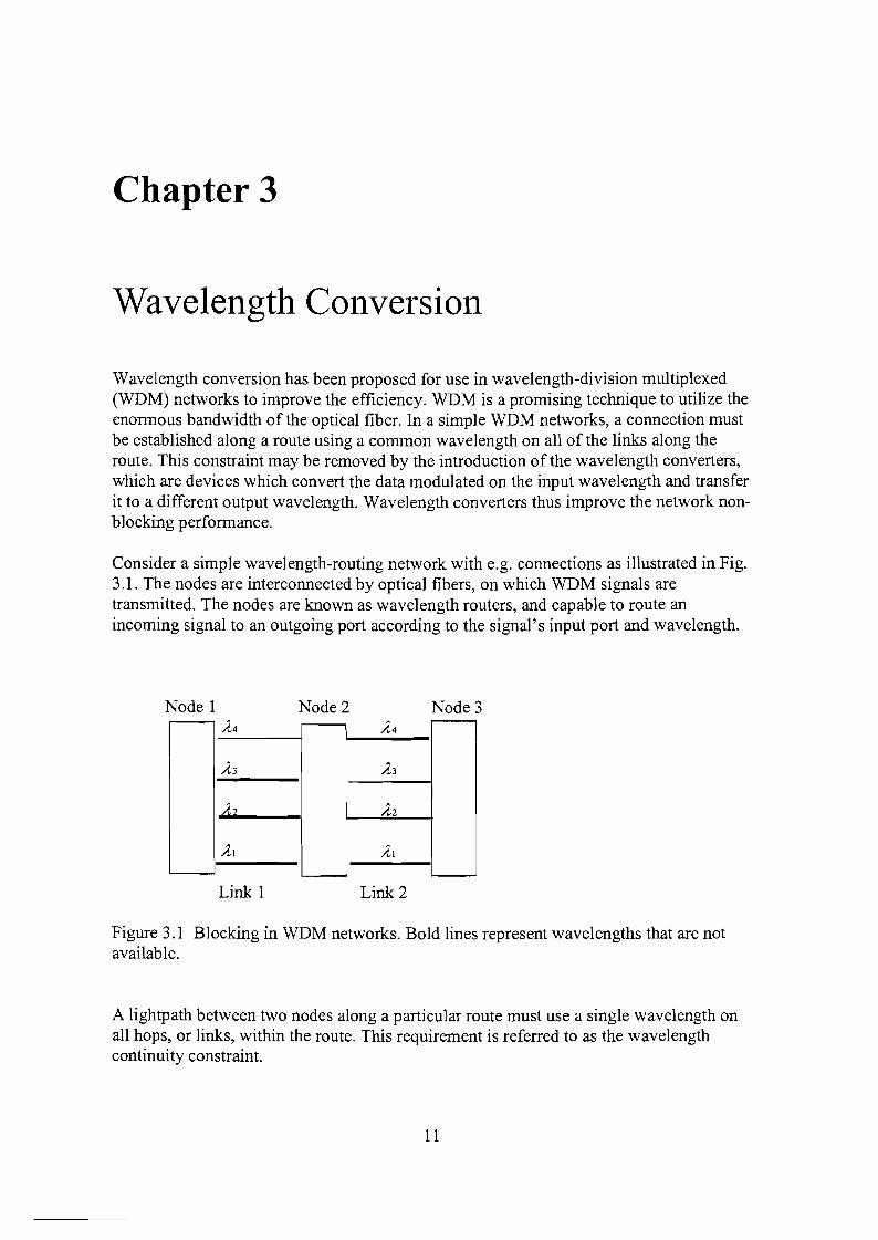
Wavelength conversion has been proposed for use in wavelength-division multiplexed(WDM) networks to improve the efficiency. WDM is a promising technique to utilize theenormous bandwidth of the optical fiber. In a simple WDM networks, a connection mustbe established along a route using a common wavelength on all of the links along theroute. This constraint may be removed by the introduction of the wavelength converters,which are devices which convert the data modulated on the input wavelength and transferit to a different output wavelength. Wavelength converters thus improve the network nonblocking performance.
Consider a simple wavelength-routing network with e.g. connections as illustrated in Fig.3.1. The nodes are interconnected by optical fibers, on which WDM signals aretransmitted. The nodes are known as wavelength routers, and capable to route anincoming signal to an outgoing port according to the signal's input port and wavelength.
Node 1 Node 2 Node 3.,1,4 .,1,4
.,1,3 .,1,3
.,1,2 .,1,2
AI Al
Link 1 Link 2
Figure 3.1 Blocking in WDM networks. Bold lines represent wavelengths that are notavailable.
A lightpath between two nodes along a particular route must use a single wavelength onall hops, or links, within the route. This requirement is referred to as the wavelengthcontinuity constraint.
11
Imagine that a connection is to be established between node 1 and node 3 along a routewhich passes through a cross-connect at node 2. This connection can only be establishedif the same wavelength is available on both links. Ifonly wavelength Al is available onlink 1, and only wavelength A2 is available on link 2, then the connection cannot beestablished.
The restriction imposed by wavelength continuity constraint can be avoided by the use ofwavelength conversion (also referred to as wavelength translation or wavelengthchanging).Ifwavelength converters are included in the cross-connect in WDM networks,connections can be established without the need to find an unoccupied wavelength whichis the same on all the hops making up the route. For instance, from Fig. 3.1, theconnection could be established using wavelength A4 on link 1, and wavelength A3 onlink 2. Wavelength converters thus result in improvements in the network performance.
A summary of different wavelength conversion schemes is given below (according to[20]).
1) Optical Electronic Conversion (O/E)
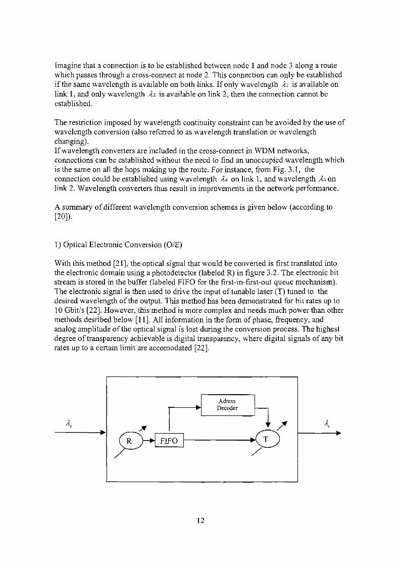
With this method [21], the optical signal that would be converted is first translated intothe electronic domain using a photodetector (labeled R) in figure 3.2. The electronic bitstream is stored in the buffer (labeled FIFO for the first-in-first-out queue mechanism).The electronic signal is then used to drive the input of tunable laser (T) tuned to thedesired wavelength of the output. This method has been demonstrated for bit rates up to10 Gbit/s [22]. However, this method is more complex and needs much power than othermethods desribed below [11]. All information in the form of phase, frequency, andanalog amplitude of the optical signal is lost during the conversion process. The highestdegree of transparency achievable is digital transparency, where digital signals of any bitrates up to a certain limit are accomodated [22].
...Adress
Decoder -
12
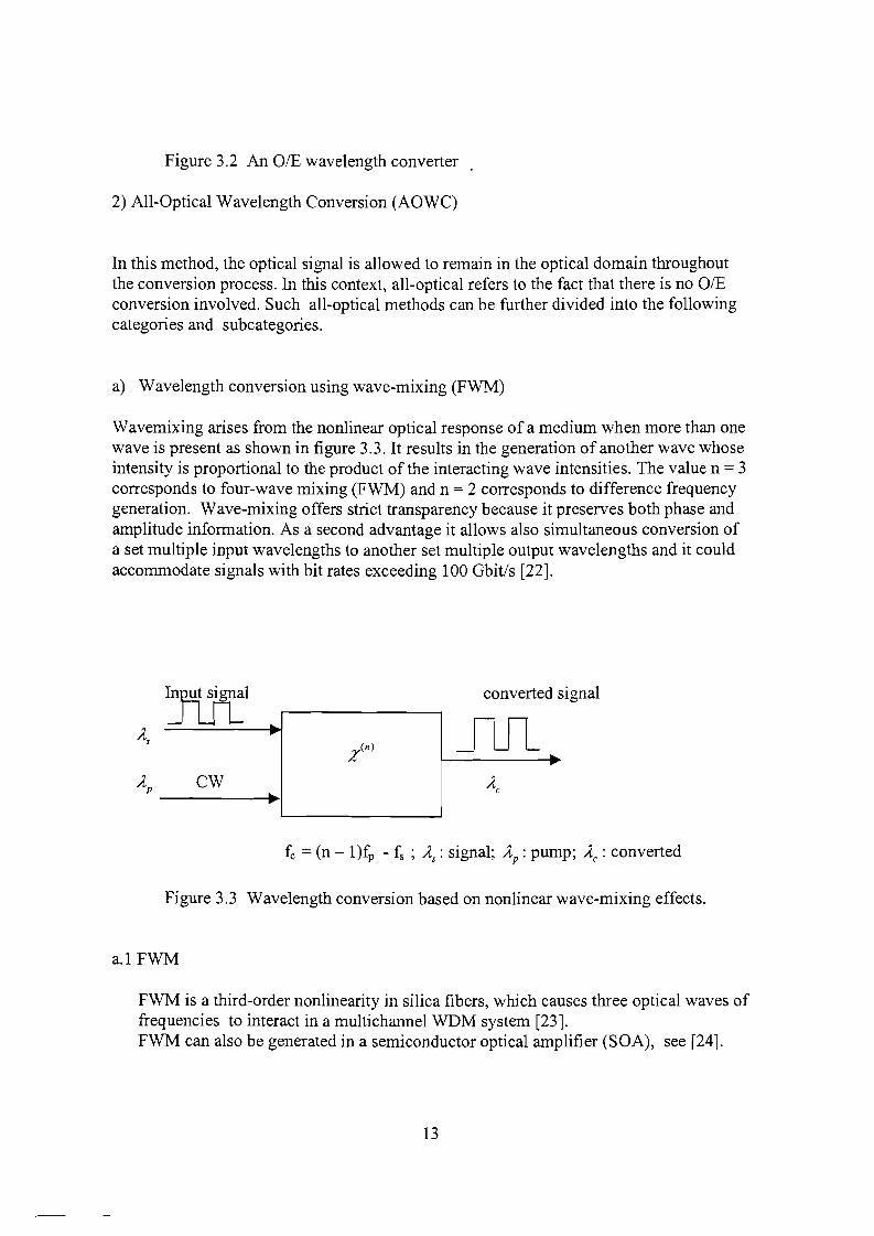
Figure 3.2 An OlE wavelength converter
2) All-Optical Wavelength Conversion (AOWC)
In this method, the optical signal is allowed to remain in the optical domain throughoutthe conversion process. In this context, all-optical refers to the fact that there is no OlEconversion involved. Such all-optical methods can be further divided into the followingcategories and subcategories.
a) Wavelength conversion using wave-mixing (FWM)
Wavemixing arises from the nonlinear optical response ofa medium when more than onewave is present as shown in figure 3.3. It results in the generation of another wave whoseintensity is proportional to the product of the interacting wave intensities. The value n = 3corresponds to four-wave mixing (FWM) and n = 2 corresponds to difference frequencygeneration. Wave-mixing offers strict transparency because it preserves both phase andamplitude information. As a second advantage it allows also simultaneous conversion ofa set multiple input wavelengths to another set multiple output wavelengths and it couldaccommodate signals with bit rates exceeding 100 Gbit/s [22].
rnMI converted signal
_ILIl.A.. ..X(n) ..
Ap CW Ac~
fc = (n - I)fp - fs ; A.. : signal; Ap : pump; Ac : converted
Figure 3.3 Wavelength conversion based on nonlinear wave-mixing effects.
a.I FWM
FWM is a third-order nonlinearity in silica fibers, which causes three optical waves offrequencies to interact in a multichannel WDM system [23].FWM can also be generated in a semiconductor optical amplifier (SOA), see [24].
13
The drawback of this technique, however, is the conversion efficiency (not veryhigh). It deteriorates with increasing conversion span (shift between pump and outputsignal wavelengths)
a.2 Difference frequency generation (DFG)
DFG is consequence of a second-order nonlinear interaction of medium with twooptical waves: a pump wave and a signal wave. This technique offers a full range oftransparency without adding excess noise to the signal but it suffers from lowefficiency [22].
b) Wavelength conversion using cross modulation
These techniques take advantage of active medium of semiconductor optical amplifiersand still belong to the category of optical-gating wavelength conversion [22].
b.1 Cross-gain modulation (XGM) in SOA.
The principle is as follows: The intensity modulated input signal modulates the gainin the SOA due to gain saturation. A continuous wave (CW) signal at the desiredoutput wavelength is modulated by the gain variation so that it carries the sameinformation as the original input signal. Further, the input signal and the CW signalcan be launched either co- or counter-directionally into the SOA. XGM SOA issimple to realize and offers penalty-free conversion at 10 Gbit/s [11]. But it suffersfrom inversion of the converted bit stream and degradation of its extinction ratio(ER) for input signal up-conversion to a signal of equal or longer wavelength.
b.2 Cross-phase modulation (XPM) in SOA.
The principe is as follows: An incoming signal that depletes the carrier density willmodulate the refractive index and, as a consequence, this results in phase modulationof a CW signal coupled into the converter. XPM is actually based on the fact that therefractive index is dependent on the carrier density in its active region. The SOA canbe integrated into an interferometer so that an intensity modulated signal formatresults at the output of the converter. This has been proposed, for instance, by:
•
•
M. Eiselt, W. Pieper and H. G. Weber, "Decision gate for all-optical retiming usingsemiconductor laser amplifier in a loop mirror configuration", Electron. Lett., vol. 29,pp. 107-109, Jan 1993.
B. Mikkelsen et aI., "Polarization insensititve wavelength conversion of 10 Gbit/ssignals with SOA's in a Michelson interferometer", Electron. Lett., vol. 30, pp. 260261, Feb. 1994.
14

• T. Durhuus et aI., "All optical wavelength conversion by SOA's in a Mach-Zenderconfiguration", IEEE Photon. Technol. Lett., vol. 6, pp. 53-55, Jan. 1994.
15
Chapter 4
Cross Gain Modulatiol1
4.1 Introduction
An optical gate can be realized by a semiconductor optical amplifier in which the gainsaturation due to an optical input signal is used to control the gain and thereby the state ofthe gate. The resulting converter is called a cross gain modulated (XGM) converter.
The input power of a semiconductor optical amplifier is the sum of two beams, one at thewavelength kw a continuous wave (CW) power, the other at As a pulse pattern. This isthe configuration of wavelength converter SOA using cross gain modulation. The CWpower can be left to co-propagate with the signal by injection at the same facet as thesignal power, or to counter-propagate by injection at the opposite facet. The XGMscheme gives a wavelength converted signal that is inverted compared to the input signal.
The discussion about XGM converter should begin with theory and modeling, whichcover the basic equations and the scattering losses. The model used here followsreference [9]. Based on this sections, given the definitions and assumptions, thetransmission function for large and small signal can be evaluated.
The solutions of the large-signal analysis can be used to find the optimal conditions thatmaximize the signal-to-noise (SNR) ratio of the converted output signal whenconsiderations include the output extinction ratio (ER). The SNR can be calculated byusing reference [12]. It means, that knowing the gain saturation function, the range of theconverted wavelength can be defined for which the SNR decreases much less then 3 dB.
Optimal conditions can be categorized by determining
the wavelength dependencethe input power dependence andthe bias current dependence (which will only be discussed).
As a criterium for optimal operating conditions the ER at the output of wavelengthconversion is considered.The solution of the large signal analysis also gives the possibility to simulate thewaveform of the probe output power.
16

The solutions to the small signal analysis can be used to study the dynamic response ofthe XGM converter, such as
• conversion efficiency; the ratio of the converted signal to the input signal,• pulse form conservation and propagation effects.
To evaluate the theory, a model for the gain must be given first and essential parameterwill be retrieved from measurements. This will be covered in this chapter.
Based on the discussion in this chapter, the simulation of some performance parameterswill be compared with the result of measurements and this will be treated in the chapterfive.
17
4.2 Theory and Model [9}
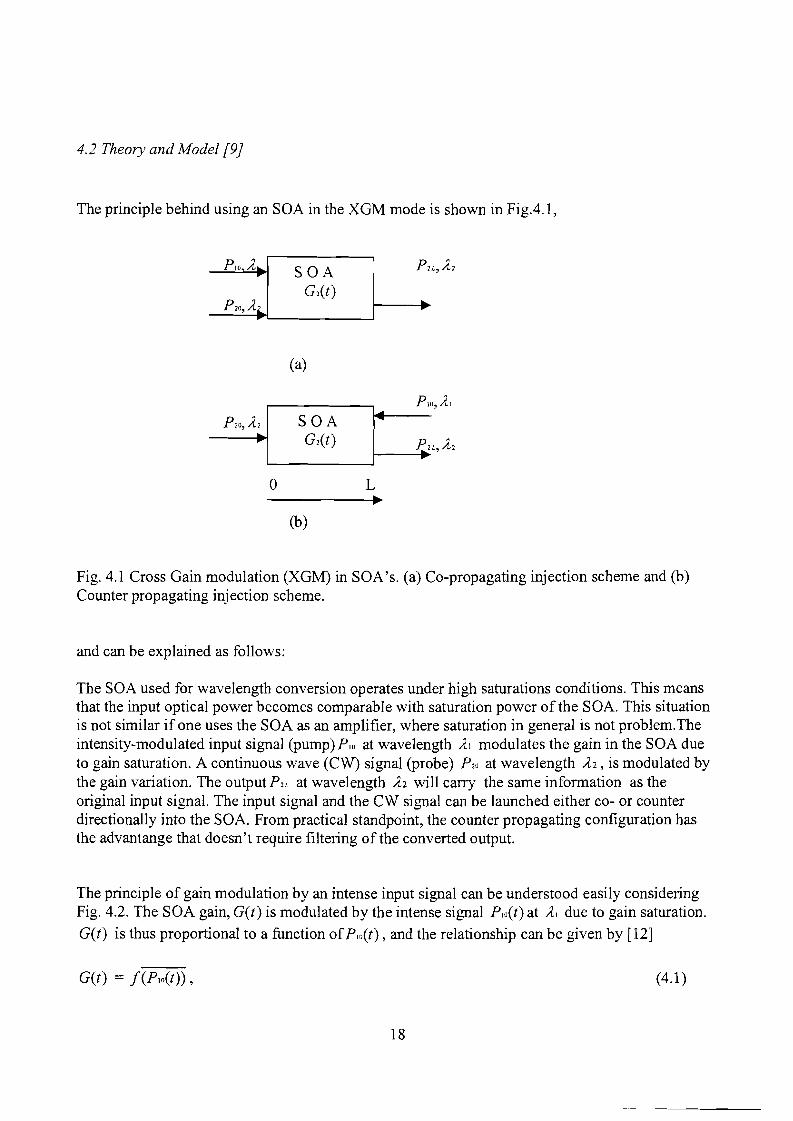
The principle behind using an SOA in the XGM mode is shown in FigA.l,
...
(a)
PIO, ;L....
P2o,A2 SOA... G2(t) Pn, A2
r
0 L~
(b)
Fig. 4.1 Cross Gain modulation (XGM) in SOA's. (a) Co-propagating injection scheme and (b)Counter propagating injection scheme.
and can be explained as follows:
The SOA used for wavelength conversion operates under high saturations conditions. This meansthat the input optical power becomes comparable with saturation power of the SOA. This situationis not similar if one uses the SOA as an amplifier, where saturation in general is not problem.Theintensity-modulated input signal (pump) PIO at wavelength Al modulates the gain in the SOA dueto gain saturation. A continuous wave (CW) signal (probe) P20 at wavelength A2, is modulated bythe gain variation. The outputPlL at wavelength A2 will carry the same infonnation as theoriginal input signal. The input signal and the CW signal can be launched either co- or counterdirectionally into the SOA. From practical standpoint, the counter propagating configuration hasthe advantange that doesn't require filtering of the converted output.
The principle of gain modulation by an intense input signal can be understood easily consideringFig. 4.2. The SOA gain, G(t) is modulated by the intense signal PlO(t) at Al due to gain saturation.
G(t) is thus proportional to a function ofPIO(t) , and the relationship can be given by [12]
G(t) = f(PlO(t)) ,
18
(4.1)
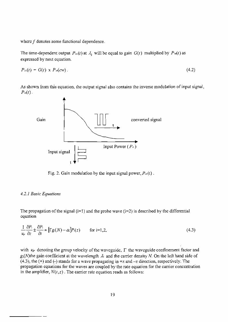
where f denotes some functional dependence.
The time-dependent output P2L(t) at Az will be equal to gain G(t) multiplied by P20(t) as
expressed by next equation.
P2L(t) = G(t) X P20(CW) . (4.2)
As shown from this equation, the output signal also contains the inverse modulation of input signal,PIO(t) .
Gain converted signal
Input signal 1str--
Input Power ( PiO )
Fig. 2. Gain modulation by the input signal power, PiO (t) .
4.2.1 Basic Equations
The propagation of the signal (i=l) and the probe wave (i=2) is described by the differentialequation
1 BPi aPi [ 10--±-= fg,(N)-ay-,(z)Vw az at for i=1,2, (4.3)
with Vgr denoting the group velocity of the waveguide, f the waveguide confinement factor andgj(N)the gain coefficient at the wavelength Ai and the carrier density N. On the left hand side of(4.3), the (+) and (-) stands for a wave propagating in +z and -z direction, respectively. Thepropagation equations for the waves are coupled by the rate equation for the carrier concentrationin the amplifier, N(t,z) . The carrier rate equation reads as follows:
19
aN I "rg;(N).-=--R(N)-SASE(N)- L P;(z) forl=1,2at eV i~I,2 Ahc/A,
(4.4)
where I denotes the injected current, e the electron charge, V and A the active region volume andcross section, respectively, and hc / h the photon energy at h. R(N) accounts for the carrierconsumption due to spontaneous radiative and nomadiative recombination, and SAsdNJ representsthe depletion due to the amplification of the spontaneous emission.
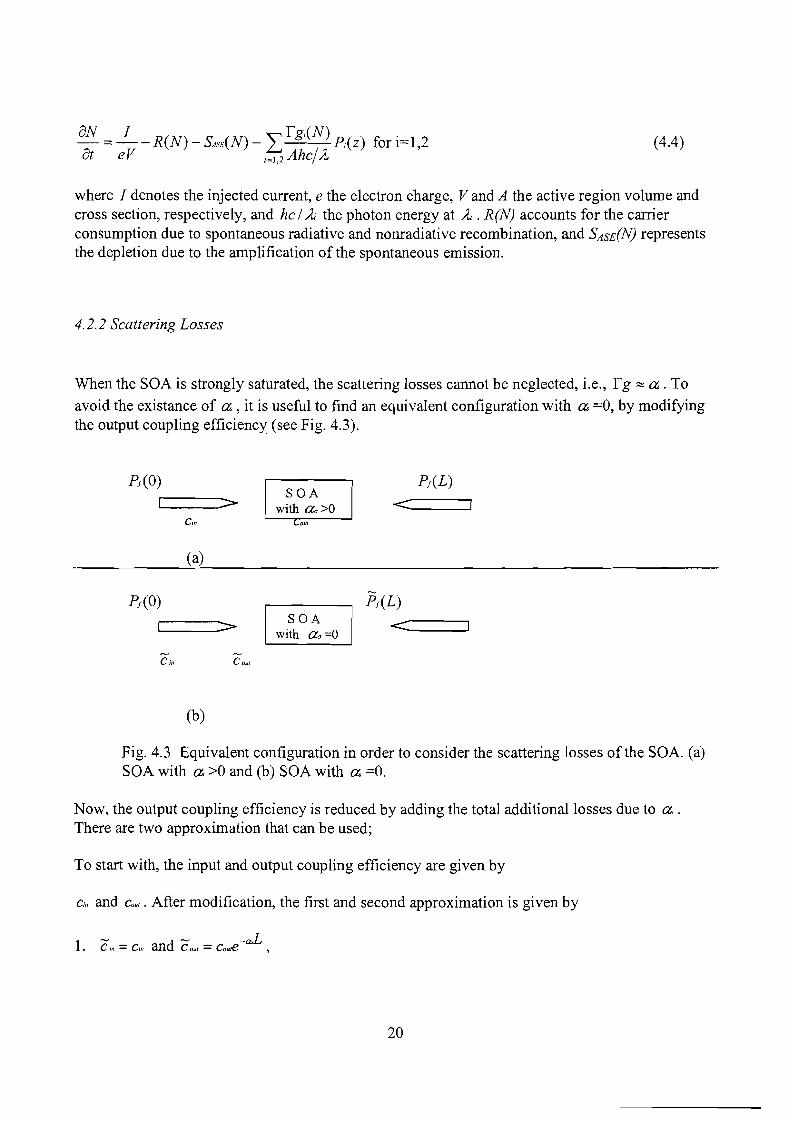
4.2.2 Scattering Losses
When the SOA is strongly saturated, the scattering losses cannot be neglected, i.e., rg ~ a. To
avoid the existance of a , it is useful to find an equivalent configuration with a =0, by modifyingthe output coupling efficiency (see Fig. 4.3).
PI(O)SOA
PI(L)
>- with a~>O <Cin (,,"0141
(a)
Pr(O) Pr(L)SOA <>- with a~=o
Cill CaUl
(b)
Fig. 4.3 Equivalent configuration in order to consider the scattering losses of the SOA. (a)SOA with a >0 and (b) SOA with a =0.
Now, the output coupling efficiency is reduced by adding the total additional losses due to a.There are two approximation that can be used;
To start with, the input and output coupling efficiency are given by
c;" and Cou,. After modification, the first and second approximation is given by
1 ~ d~ -aL. Cm =c;" an Cou, = cou,e ,
20
2 ~ / d ~ -aL. c", =Cia Cadd an C ou' =Cou,Cadde ,
respectively.
The expression for C"dd has been found empirically and can be expressed as
-O.32aLCadd ~ e .
This modification can be inserted into the calculation through the fiber-to-fiber gains
GfT =Pr(L)/Pr(O) and OfT = Pr(L)/PJ(O). That is allowed as the expression of the saturated gain is
related to the dependence of the gain and input power.
21
4.3 Transmission Function
4.3.1 Definitions and Assumptions
It is always usefull to introduce first some definitions that are used in this report and they are
• Gi =XiL 1XiO; denotes the saturated gain and
• G =exp([gi(N)L) ; denotes the unsaturated single-pass gain at Ai . The parameter
• jJ:= gNI ; accounts for the ratio of the differential gains at AI and ,,1,2, which is an importantgN2
quantity for XGM.
• Except for counter propagating injection, the single pass gain signal must be modified andgiven by
GI = xlOl XIL, where XIL =PIO/p sal•
• Because the N(t,z) is not unifonn along the device, it is convenient to introduce an average
carrier density according to1 L
Na,(t):=- fN(t,z)dz (4.5)L o
• The nonnalized power
X,(z) := Pi(Z) 1P,'OI
• the internal saturation power of the amplifier is given by
Pi '01 = Ahc 1([ r;gNih)
The assumptions which have been taken to analyze the XGM SOA are
(4.6)
1. The gain coefficient gi(N) depends linearly on the carrier density, i.e.,
g,(N, A) = gNi(A)[N - NOi(A)] , with both the differential gain gNi and the carrier density at
22
transparency N Oi being wavelength dependent in order to consider the spectral dependence ofthe unsaturated gain and the nonunifonn saturation of the gain.
2. The spontaneous radiative and nonradiative recombination rate can be linearized according toR(N) = N /,r; (with r; denoting the spontaneous carrier lifetime).
3. The carrier consumption due to the amplification of the spontaneous emission is negligible(SASE =0) .
4. The scattering losses of the SOA is considered as modified coupling efficiencies (a =0).
5. The transit time of the SOA is short compared to the bit period, i.e.,
6. The temporal derivative of the carrier density due to the modulation of the signal is negligible,i.e., iN/ot = o.
By inserting (4.4) into (4.5), the average carrier density can be given (see appendix A.I) as
iNav(t) _ N _ N ( ) _ " xi(L) - x,(O)r; - av t L..J '
a ;=1,2 rgNL
where N = I r; I(eV) represents the unsaturated carrier density.
Integrating (4.3) from zero to L, and with the 5th assumption yields
[P,(t ,L) ] [ ]In =rgNL Nav(t) - NOi ,P,{t,O)
and in its nonnalized fonn, from (4.6) is given by
[X,(t,L)] [ ]In. =rgNL Nav(t) - No, .x,(t,0)
23
(4.7)
(4.8)
(4.9)
The input field of a semiconductor optical amplifier is the sum of the two beams, one at thewavelength Acw, a continuous wave (CW) field, the other at A.r, a pulse pattern.
Let a small-signal modulation be superimposed to the one of the input power, Xi(t,O) , as given by
( 0) - - jaJIXi t, - Xio + XiOe + C.C. (4.10)
Since the amplifier is operating under saturation, the carrier density, Nav(t) is accordingly also
modulated (consequently, also the gain) and can be given by
No,(t) = No, + Na..e jaJI + c.c.
The output power of the amplifier consequently becomes also time-dependent signal
( L) - - jaJIXi t, - XiL + XiLe + c.c.
. h P IP,a, d P IP,a,WIt x.o == iO j an XiL == ,L j •
(4.11)
(4.12)
Inserting (4.10)-(4.12) into (4.7) and (4.9) yields the transmission function for the large-signal(stationary solution) as well as for the small-signal (oscillatory solution) and they both arerepresented in the next section.
4.3.2 THE LARGE-SIGNAL ANALYSIS
The large-signal analysis of wavelength conversion based on cross-gain modulation in asemiconductor optical amplifier is developed in this section, for the case in which pump and probeare injected from the same and opposite facet, respectively.
The solutions for the large-signal analysis is given below and detailed derivations can be found inthe appendix A.2 (Co-Propagating) and A.3 (Counter Propagating)
{( Gl)l/fJ
_ } 1 [ (Gl) ]Gl G2-1 = fJx20 In Ci: -xlO(Gl-1)
and
24
(4.13)
(4.14)
and
{(~:rG, -I} ~ :,H~:J-X,.(G, -1)] ~~ Counter Propagating
Equation (4.16) represents the nonlinear transmission function for cross-gain modulationG2 = f(xlO). The only parameters needed for the calculations are:
• X20
• jJ
• Gl
• and G2.
4.3.3 THE SMALL-SIGNAL ANALYSIS
(4.15)
(4.16)
This section gives a small-signal analysis of wavelength conversion.From the definitions given in the previous section, transmission function for small-signalsuperimposed on the opticals power in counter scheme can be given by (for derivations of thisequation, see appendix B.1 for co-propagating and appendix B.2 for counter propagating)
where
a(lV) =1- (G2-1)x2o- (@+ jm)"and
And the 3dB bandwidth, lUi ,is given by
25
(4.17)
(4.18)
(4.19)
1+ GIXIL + G2X20cv.=------
The effective carrier lifetime is given by
] r;Z;, err =- =-----
. cv. 1+ G,XIL + G2X20
4.3.4 Gain Model
(4.20)
(4.21)
To avoid complexity of the gain calculation, one needs to take the needed parameters such as the
unsaturated gain G I, G 2 and fJ (see 4.13-4.16) from measurement.
Some definitions should be first given, namely
• normalized unsaturated gain coefficient
• normalized differential gain
The spectral dependence of ag and bg can be approximated by a second order polynomial
(4.22)
(4.23)
(4.24)
(4.25)
where Amax is the wavelength which the unsaturated gain coefficient reaches the maximum. The
unsaturated gains G, and the parameter fJ are related to ag and bg as given by
G(h) =ergi(N)L
rg(N,JJ)L g(N,A.",,)=e g(N,A. ..,,)
26
=efg(N,A. max)L.ag(,l,)
= G ag(,l,)milX
and
with G max =efg(N,A.max)L denoting the unsaturated gain at A max.
(4.26)
(4.27)
By measuring the spectral dependence of the unsaturated single pass gainGdB(A) yields A max and G max. Using (4.24) and performing a quadratic fit with respect to the
measured curve, the coefficient Q2 can be found.
As stated from the assumptions, the gain coefficient is linearly dependent on the carrier density.The carrier density is supplied by drive current.Thus, if the current is changing from one value to another value, the gain coefficient must alsolinearly changing according to the current value.Measuring the gain coefficient curve for different current values, the unsaturated single pass gain indB for any injection current can be expressed as
(4.28)
where GdB./(A) denotes the unsaturated gain at A for the injection current I, which is different from
the value adjusted for GdB(A) above.
After that, a linearly fitting has to be performed from the measured values of G dB. I(A) as a function
of GdB./(Amax) for various injection current to obtain the parameter bg(A). Knowing the various
values of bg(A), the coefficients b, and b2 can be extracted by fitting a parabolic curve.
Thus, as soon as the parameters needed for the calculations
• X20,
• fl,
are determined, the nonlinear transmission function for cross-gain modulation G2 = f(xlO) can befound.
27
4.4 Extinction Ratio (ER) and Signal-to-Noise Ratio (SNR)
The extinction ratios and signal-to-noise ratios are the two main figures-of-merit for a wavelengthconverted signal and are determined by accounting for gain saturation and spectral shifting whichoccur due to the depletion of the injected carrier density.
From previous section, the saturation probe gain equation was already found.The output extinction ratios (ER) can be evaluated from G, = f(xlO) for bit rates up to B« 1/Ts,eifaccording to the assumptions (3) and (5).
The equation (4.2) gives that, since the signal wave is intensity modulated withXIO = ~;; : x;t }, the probe gain is also modulated. Thus, the output extinction ratios, which is equal
to the ratio of the probe gain of "1" and "0" bits at the probe wavelength, is given by
with
Gon-G( off)2 - ,xlO
and
GOff -G ( on)2 - 2 X lO •
Or, the ERuul can also be expressed as a function of the input extinction ratio
and the average input power
( on off)(x,,) = x lO + x lO •
2
The overall SNR is given by [12]
28
(4.29)
(4.30)
(4.31)
(4.32)
(4.33)
SNR = ,..--''----.L-...,-,-- (4.34)
where S"I" and S"O" are detected probe output signals for the "1" and "0" bits, respectively.Substituting the parameters for the probe output and the noise terms,
N =Nshol + Nt + Ns - sp + Nsp- sp ,
where we discern the following contributions
• Nshot is the shot noise
2(G2P20 JNshot =2Bee -;;;;- + nsp(G -l)Bo a.
• Nt is the thermal noise in the receiver
Nt = e24kTR
• Ns - sp is the detected probe-spontaneous beat noise
• Nsp- sp is the spontaneous-spontaneous beat noise
Nsp- sp = (en,p(G -l)ayBe(2Bo - Be)
The SNR can be now given by
SNR = (G:'I"P20 - G:'O"PIOY
(h vBe) J4n:~"(G:~")2 P20 + ~4n:~0" (G:~0")2 P20
(4.35)
(4.36)
(4.37)
(4.38)
(4.39)
(4.40)
Bo is the bandwidth of the optical filter, Be is the electrical bandwidth of the receiver and aincludes all the optical loss between the output of the converter and the detector. Each noise term isdifferent for the probe gain corresponding to the "1" and "0" bits.
Assuming that
29
• the noise is only dominated by signal-spontaneous beat noise sincethe converter signal uses preamplification when reaching its destination node
• and G» 1,
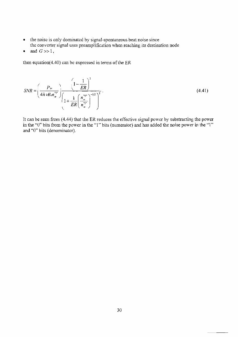
then equation(4.40) can be expressed in terms ofthe ER
SNR =( P20 J (l-~r4h v13en:~" [ _1«0" J-1/2 J2 .
1+ ER n"l"'p
(4.41)
It can be seen from (4.44) that the ER reduces the effective signal power by substracting the powerin the "0" bits from the power in the "1" bits (numerator) and has added the noise power in the "1"and "0" bits (denominator).
30
4.5 Dynamic response
From (4.21), it is obviously that all dynamic processes should be governed by aneffective carrier lifetime T:, eff ,i.e., the spontaneous carrier lifetime which is reduced due tothe stimulated emission ofthe signal and the probe power.
This equation suggest that increasing the optical power within the amplifier speeds up thedevice reponse as recombination rates are increased due to stimulated emission. Otherfactors that can be used to increase the modulation bandwidth is that the SOA should beoperated with
large current injection,large optical confinement factor andlarge differential gain.
In case of zero modulation ofthe probe XlO at the input,i.e., XlO =0,the normalized power modulation for the signal and probe can be expressed by
- _ [G G.(GI -l)XIO]_XIL - 1- ( .) XIO
m,+}OJT:
and
respectively, see appendix C.
(4.42)
(4.43)
Since the expression in the bracket of equation (4.42) is positive, a comparison ofequations (4.42) and (4.43) reveals that the modulation on the signal and the probe areout of phase. The two equations also show that the signal XIL is high- pass filtered, sincea low pass transfer function is subtracted from the constant single pass gain GI, whereasthe probe Xl[ is low-pass filtered.
For the signal, it means that due to the saturation, the low frequencies of the input signalwill be filtered away as the signal propagates through the amplifier. Therefore, themodulation that is transferred to the probe signal in the output (L) of the amplifier has apredominant high frequency content that equalizes the modulation that is experienced inthe input side (0) of the amplfier.
31
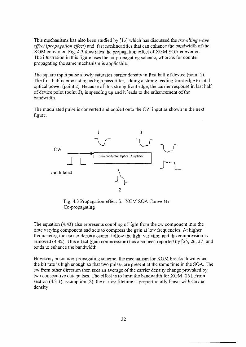
This mechanisms has also been studied by [13] which has discussed the travelling waveeffect (propagation effect) and fast nonlinearities that can enhance the bandwidth of theXGM converter. Fig. 4.3 illustrates the propagation effect of XGM SOA converter.The illustration in this figure uses the co-propagating scheme, whereas for counterpropagating the same mechanism is applicable.
The square input pulse slowly saturates carrier density in first half of device (point 1).The first half is now acting as high pass filter, adding a strong leading front edge to totaloptical power (point 2). Because of this strong front edge, the carrier response in last halfof device point (point 3), is speeding up and it leads to the enhancement of thebandwidth.
The modulated pulse is converted and copied onto the CW input as shown in the nextfigure.
1 3
modulated
CWv Vv
==I-~I-_-"~I_s_effil_._co_nd_u_ct_or_o_Pt_ic_al_A_m_Pl_ifi_er__1
2
Fig. 4.3 Propagation effect for XGM SOA ConverterCo-propagating
The equation (4.43) also represents coupling oflight from the cw component into thetime varying component and acts to compress the gain at low frequencies. At higherfrequencies, the carrier density cannot follow the light variation and the compression isremoved (4.42). This effect (gain compression) has also been reported by [25, 26, 27] andtends to enhance the bandwidth.
However, in counter-propagating scheme, the mechanism for XGM breaks down whenthe bit rate is high enough so that two pulses are present at the same time in the SOA. Thecw from other direction then sees an average of the carrier density change provoked bytwo consecutive data pulses. The effect is to limit the bandwidth for XGM [25]. Fromsection (4.3.1) assumption (2), the carrier lifetime is proportionally linear with carrierdensity
32
1-ocN.r;
If two consecutive pulses presents at the same time, the average carrier density becomessmaller and consequently the carrier life time in SOA is increased.The result is that the bandwidth would be reduced.
It is also important to note that the bandwidth can be increased by increasing the length ofthe amplifier. The best improvement can be seen in co-propagating scheme, whereas forthe counter-propagating, the bandwidth will decrease with increasing the SOA length.This decreasing is due to the dephasing effects.If the length of the SOA to long, at high bit-rates, the transit time becomes longer thanthe bit period of the data signal. The gain of the SOA at any instant is, for the signalpropagating from other direction, determined by the data signal power averaged over anumber ofbit periods.
The behaviour of the frequency response of the wavelength conversion, from (4.43),
(4.44)
can now be seen to be based on a combination of the device gain and carrier lifetime andalso resembles a low pass filter.
33
Chapter 5
Measurement and Simulation
This chapter provides the setup and the measurement for XGM wavelength conversion.In the first place, the static measurement will be carried out to define
• the unsaturated gain peak and the peak wavelength;By this measurement, the unsaturated gain is measured for difference currents(needed for simulation) and difference input powers.
• the polarization dependency;A polarization sensitive SOA will complicate the system performance. Polarizationindependence is ensured if the SOA gain is designed to be polarization independent.The polarization dependence originates from differences in the confinement factorsand in the differential gains.
• the saturation power of the semiconductor optical amplifier at the given wavelengthoperation (in this project thus, 1551 nm and 1540.53 nm). The knowledge ofthesaturation power is essential as the pump signal will have a significant impact on thegain modulation near this saturation power. The saturation power anyway is whenthe input power become equal with the internal saturation power for thesemiconductor optical amplifier (SOA) and consequently the gain decreases about 50% from its peak value. This effect is known as gain saturation and can be used toconvert data from one wavelength to another as already stated in the previouschapters.
In the second place, dynamic measurement would be done to define
• the extinction ratio (ER) of input pump signal and the output probe signal (convertedsignal)
• bit error rate measurement (BER) to examine the performance of the transmission andto define the power penalty.
The experiments are performed based on the 1550 nm Bidirectional Laser Amplifier.For details characterstics, see appendix 1.
34
5.1 Static Measurement
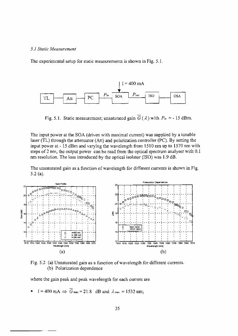
The experimental setup for static measurements is shown in Fig. 5.1.
1= 400 rnA
'---_:----1l..-_---JI--
P-
o
-
ur-[:J-1 OSA I
Fig. 5.1. Static measurement; unsaturated gain G (A) with Pin = - 15 dBm.
The input power at the SOA (driven with maximal current) was supplied by a tunablelaser (TL) through the attenuator (Att) and polarization controller (PC). By setting theinput power at - 15 dBm and varying the wavelength from 1510 nm up to 1570 nm withsteps of 2 nm, the output power can be read from the optical spectrum analyser with 0.1nm resolution. The loss introduced by the optical isolator (ISO) was 1.9 dB.
The unsaturated gain as a function of wavelength for different currents is shown in Fig.5.2 (a).
1=400mA -- ... --t
1=300mA I I
1=200mA
t I I I
12 - -I - - ,. .. - 1- - ., - - l'- - -j 0
I : I I I I X10L~-:"-~""; __~";"::::::;::=o::=::;:==:'-~...,;j1510 1515 1520 1525 1530 1535 1540 1545 1550 1555 1560 1565 1570
W.",lenglh lnm)
(a)
Polarization Dependence24.----.-----.--.---.-----.-,-.--.........---.--,..-""'!""'"--;--,
,,
22 - - :- - -~-~0:0~~ci0 ~ ~ ~~ - - ;- - -;- - -: - - : - -100"" I I I I ,DOt!) I I I
O' I I I I I I t DDl I I
20 13 .. ~7'";)~:'-',7,,;:7 ., _ .. : .... r- _ .. ~ .. -:ctt:tb- - ~ ....\Y. I I I Y I I • D I
I I I I I T I I DID~ 18 .... ;_ .... ;_ .. _: __ ~ .... ~ .... : .... ~ - .. ~~~ .. J -
I I I I,16 .... ;- - - .... -: .... -: .... ~ - - +.... r .. -:- .. -1- ...... - ~ - y-
8 ~~~tC~;e: :'14L~__=-=,..:-:_:-:_:7:,_'""_'""_"',_-=-,_~ .... ; .... ~ .... ~ .... ~ .... :- - -: .... ~ .. -
I I I I I I I I I
I I I I I I
I I I I
1f5L.:-10-1~51-:-5~'5"'::".20:"""':":'152':":5-1-:':53-:-0~'5"'::".35:"""':":'154'::0~1~54-:-5~'5~50::-:-:15'::55~1~56::-0~156~5~15'70W.",lenglh [nmj
(b)
Fig. 5.2 (a) Unsaturated gain as a function ofwavelength for different currents.(b) Polarization dependence
where the gain peak and peak wavelength for each current are
• 1= 400 rnA => Gmax = 21.8 dB and Amax = 1532 nm;
35
• I = 300 rnA => Gmax = 20.5 dB and Amax = 1534 nm;
• I = 200 rnA => Gmax = 17.14 dB and Amax = 1546 nm;
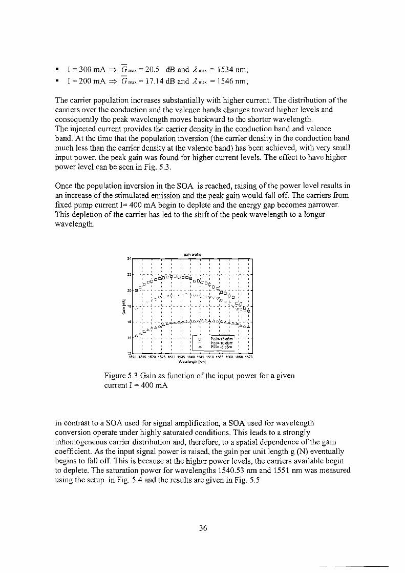
The carrier population increases substantially with higher current. The distribution of thecarriers over the conduction and the valence bands changes toward higher levels andconsequently the peak wavelength moves backward to the shorter wavelength.The injected current provides the carrier density in the conduction band and valenceband. At the time that the population inversion (the carrier density in the conduction bandmuch less than the carrier density at the valence band) has been achieved, with very smallinput power, the peak gain was found for higher current levels. The effect to have higherpower level can be seen in Fig. 5.3.
Once the population inversion in the SOA is reached, raising of the power level results inan increase of the stimulated emission and the peak gain would fall off. The carriers fromfixed pump current J= 400 rnA begin to deplete and the energy gap becomes narrower.This depletion of the carrier has led to the shift of the peak wavelength to a longerwavelength.
,I I I I I j I
22 - -: - - ~ ~ o~ "0l?1J-D~D-0-ciJ- - ~ - - ~ - -: - - ~ - -;- - ~10
0 41 I I 1 IDOla 0 rL. I I I ,
0' I I I I I ''''00' I
20 Gi -: - - ~ - - ~ ~7~~:'- ~v~;:-~ -.r\;~,~.~,~- ~;~ ~ --;0 [] ¢~ -;- . :to I , I It! , I
~ 18 1- I , I I I I I I y .... OrO I
~ \;> '-: - - : - - ;- - -: - - : - - ;- - : - - : - -: - - : ~ ~~::::'B~I I l ' I I I , t I
16 - .;- - ~ - - :~l:.-zhn~~~~4~~b.:c..64,~A:- --:I 6..66., I I 1 1 I I I lAC.&.
lAb I I' I It;, A I I I .--'_~-'--""""""" ,
14 - -;- - ~ - - ~ - -,.- -.,., - -', 0 P20=.15dBm -,- -..,P20=-1O dBm I II I: D. P20=- -5 dBm :
12l.:--~~~~~~~.:;=~~::::;:::~~1m1mlm1m1~1m1~~51B1Wl~1~1m
Walelenglh Inm]
Figure 5.3 Gain as function of the input power for a givencurrent I == 400 rnA
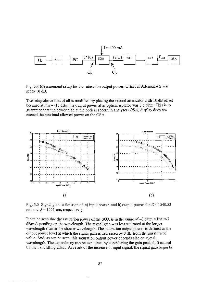
In contrast to a SOA used for signal amplification, a SOA used for wavelengthconversion operate under highly saturated conditions. This leads to a stronglyinhomogeneous carrier distribution and, therefore, to a spatial dependence of the gaincoefficient. As the input signal power is raised, the gain per unit length g (N) eventuallybegins to fall off. This is because at the higher power levels, the carriers available beginto deplete. The saturation power for wavelengths 1540.53 nm and 1551 nm was measuredusing the setup in Fig. 5.4 and the results are given in Fig. 5.5
36
1= 400 rnA
CaUl
Fig. 5.4 Measurement setup for the saturation output power; Offset at Attenuator 2 wasset to 10 dB.
The setup above first of all is modified by placing the second attenuator with 10 dB offsetbecause at Pin = -15 dBm the output power after optical isolator was 3.5 dBm. This is toguarantee that the power read at the optical spectrum analyser (OSA) display does notexceed the maximal allowed power on the OSA.
Gain Saturation
24r-ii-i-ii-t=:::::::::==::::r:::::::::;.,I I I I ,
: : : : : \ R ~~~:53n~m I22 - - -oi - - .... - - - .. - - - ... - - - 1- - - -'.-----~--'-I
,DOo¢ I I I I
/,.. , ODD I I I Ii: :: :C:'"t!~~~~i~;to: :::::;::: t:-c: I I I I I\'~\;,D¢ I I
~ 16 - - _:- - - ~ - - - ; - - - ~ - - _~ _' ;:'~/.gCl- ~ - - - : - _I I I I I I "\"180 I
I I ~~·O I
I I I I I I I \"[J I
14 - - -:- - - -: - - - ~ - - - ~ - - - ;- - - -: - - - ~ - "t~'ee --I I I I' I I
12 I I I t I I I I
------~---~---~---~---I---~---r--
" ,, ,1?''="7--~15-.""::'3- ....-"--.9~-.~7 - .....5-.....3--.''-....J
Input Power [dBm]
(a)
Gain SatuJation
24i--.-----;-----;:==r:::::=:=::::;lI 8 ~t~:g3n~m I
22 ------Cjl--------I----10 0 t:I 0 '
, ClO¢J ,
20 - - yo :::". l'" -::;z "'J-\~~ - - .. -1 -O-~Oci - - ~ - - - - - - -
, "'c', %0'
r: :::::: :,::::::::':::':>~:14 - - - - - - -;- - - - - - - -: - - - - - - - ~ - - -;~i\
, ,, , ,
12 - - - - - - -1- - - - - - - -,- - - - - - - "i - - - - - - -, ,
,ol..-----'------'----.,....---5 9 l' l'
Output 'Power ldBm]
(b)
Fig. 5.5 Signal gain as function of a) input power and b) output power for A= 1540.53nm and A= 1551 nm, respectively.
It can be seen that the saturation power of the SOA is in the range of-8 dBm < Psat<-7dBm depending on the wavelength. The signal gain was less saturated at the longerwavelength than at the shorter wavelength. The saturation output power is defined as theoutput power level at which the signal gain is decreased by 3 dB from the unsaturatedvalue. And, as can be seen, this saturation output power depends also on signalwavelength. The dependency can be explained by considering the gain peak shift causedby the bandfilling effect. As result of the increase of input signal, the signal gain begin to
37
saturate (reduction of injected carrier numbers). The carrier density decrease causes thegain peak to shift at longer wavelength according to the reverse process of bandfilling,which compensates for the decrease of gain at the longer wavelength. Therefore, thesaturation output power turns out to be higher for the longer wavelength signal.
5.1.1 Quadratic Fitting the Unsaturated Gain
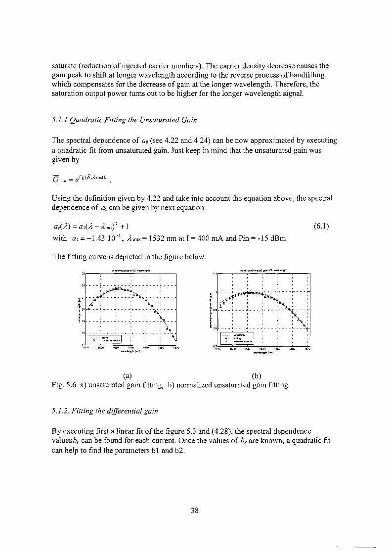
The spectral dependence of ag (see 4.22 and 4.24) can be now approximated by executinga quadratic fit from unsaturated gain. Just keep in mind that the unsaturated gain wasgiven by
G - rg(N,;(mox)Lmax - e .
Using the definition given by 4.22 and take into account the equation above, the spectraldependence of ag can be given by next equation
ag (A)=a2(A-An,"x)2+1 (6.1)
with a,=-1.431O--4, A max = 1532nmatI=400mAandPin=-15 dBm.
The fitting curve is depicted in the figure below.
,,I I I I
22 - - - I - - - - - - - -.- - - ".- .. - - i - - -I I , I
I I~'~' ,~" •• ,_ •• ~_ ••• ,.- C"'T'-'
- I I I I
~ I I , I I
:20A. __ J. ..J ' L _ _ L _
~ I I I I d~ I
2 I , I I '*.~ 19 - - .. ~ - - - -: .. .. - -: - - - - :- - - - +~ - -
I I I I I \
I I • I I li.
16 I·---=..::' ;.,~ , ~ '," , .,' . - , ~ - . - T • ,
6. measurements
?5.~OO=:;;:""':==::"'=3)=---~,s.o::----;;"~50 -::':"00:--...,.)'570'fIIB\IIe!engtl1 lnmJ
.~ ,'tI .... I I' I I
! !A: : : : : :~ 0.9 - - - ~ - - - ~ - - - -: .. - - -: - - -x----~~ I I , I I I
'i I I I I I ,
~ 0.8 ...... : ...... ~ - - .. -: - - - -; - - - -;- - -~,,
1520 1530 1540 1550 1560 1510......ngttl[nm]
(a) (b)Fig. 5.6 a) unsaturated gain fitting, b) normalized unsaturated gain fitting
5.1.2. Fitting the differential gain
By executing first a linear fit of the figure 5.3 and (4.28), the spectral dependencevalues bg can be found for each current. Once the values of bg are known, a quadratic fitcan help to find the parameters bland b2.
38
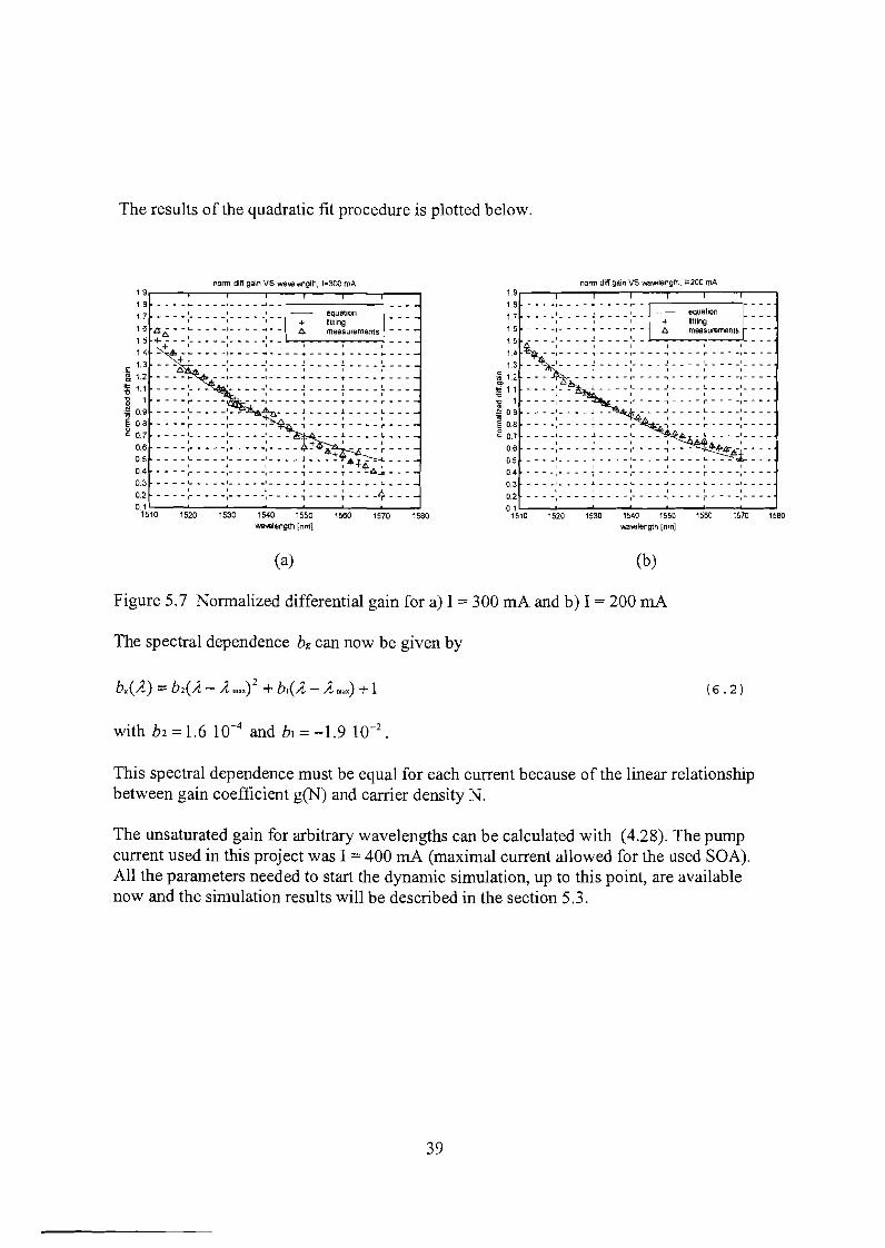
The results of the quadratic fit procedure is plotted below.
equationfillingmeasurements - - - -
+A
norm diff.gain VS wa",lenglh, 1;200 rnA1.9 ,..----........---T--r---........---T--r------.1.8 ----I----1-----r--,---------,1.7 -: ~ - - :- -1.6 _ -1- ., - 1- -
1.5 , ! I__ J.--~~~~.....,...J
1 1 1 1
1.4 - -I - - - - ., - - - - 1- - - - ., - - - - ~ - - - ·t - - - -1.3 1_ ~ __ 1 __ • _: ~ ~ __ - _ ;__ - - _; _
.~ 1.2 - - - ; - - - ,. - • - - ,- - - - ., - - - - ~ - - - -. - - - -:1.1 1 l :_~ :----~----:----
i 1 --,~---I----r----I--·-~0.9 -' L I _
~ 0.8 _. - -I - - - - 1 • - - - \- - ~ - - - - ~ - • - -: - - - -c: 0.7 .1. J. I. _ _ _ _ _ L. __ - _1 _
0.6 -.--:-.--~----:---.~--_£~~..4r"&-I.---0.5 _ - __ 1 J. 1 -' L _
1 1 1 • I t0.4 - - - -1- - - - 7 - - - -.- - - - 1 - - - - r - - - -1- - ~ -0.3 __ ~ .1 _ • __ J. 1 oJ L I __ • _
• 1 lIt 1
0.2 - - - -. - - - - 7 - - - ~ .- - - - -, - - - - r - - - -,- - - -
o115L,0,---1~52'"':0--:1.....53::-0--:'15~40:-----:-:15'::50--:1::';56::-0 --:'15:':70:---1-:-!5S·0
wa",leng1h Inm]
norm diff.gain VS wawlength, 1=300 rnA1.9,----,---r----r---,--........---,-----,1.8 - - - - I- - - - _1- __ ... _I .. _ ,-------,
1.7 1 1 -'__ equationI I t + fitting
~:: ~~ ==~ ====:= =: =~= = A measurements+ I I I I I I
1.4 I- _I_ -l .. _ ~ ..
.£ 1.3 -~ -:- -; ~ f - .. ~ -~ 1.2 .. -1- -, of I"" -
l§ 1.1 '-----:----~----~----~---'E 1 '---.----.,----T----r----:i 0.9 ~- .... ~ ; ~ -
Eco
00.'76 .. ,. T ~ -___ .1. 1,. _
0.6 I + I I
~.~ ====f====i= ====i ====~ ==~= ~ ~~~~; ===0.3 L. _1_ _I ..t .1.. L _
0.2 :- :- -~ ~ ~ -4 - ..°11-'::10:--~15:':::20:--~153:':::0:----:-:154'::0:---1~55:-0--1 56:-0--'.....57:-0---'1580
W<M!length (nm]
(a) (b)
Figure 5.7 Nonnalized differential gain for a) I = 300 rnA and b) 1= 200 rnA
The spectral dependence bg can now be given by
(6.2)
with b2 =1.6 10-4 and bl =-1.9 10-2•
This spectral dependence must be equal for each current because of the linear relationshipbetween gain coefficient g(N) and carrier density N.
The unsaturated gain for arbitrary wavelengths can be calculated with (4.28). The pumpcurrent used in this project was I = 400 rnA (maximal current allowed for the used SOA).All the parameters needed to start the dynamic simulation, up to this point, are availablenow and the simulation results will be described in the section 5.3.
39
5.2 Dynamic Measurement
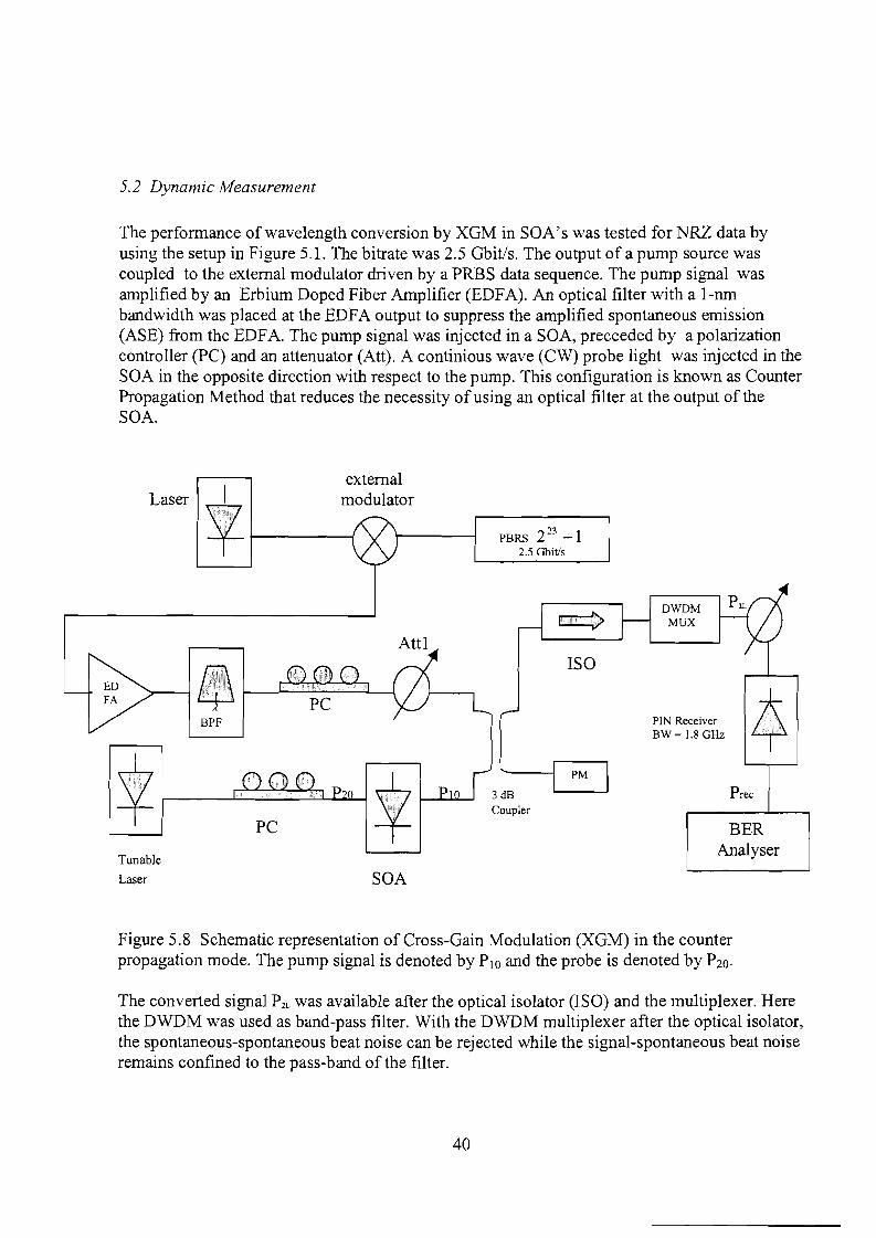
The performance of wavelength conversion by XGM in SOA's was tested for NRZ data byusing the setup in Figure 5.1. The bitrate was 2.5 Gbit/s. The output of a pump source wascoupled to the external modulator driven by a PRES data sequence. The pump signal wasamplified by an Erbium Doped Fiber Amplifier (EDFA). An optical filter with a 1-nmbandwidth was placed at the EDFA output to suppress the amplified spontaneous emission(ASE) from the EDFA. The pump signal was injected in a SOA, preceeded by a polarizationcontroller (PC) and an attenuator (Att). A continious wave (CW) probe light was injected in theSOA in the opposite direction with respect to the pump. This configuration is known as CounterPropagation Method that reduces the necessity of using an optical filter at the output of theSOA.
Laserexternal
modulator
PBRS 2 23 -12.5 Ghit/s
DWDMMUX
PIN ReceiverBW= 1.8 GHz
ISOAtt1
Tunable
Laser SOA
3 dBCoupler
Prec
BERAnalyser
Figure 5.8 Schematic representation of Cross-Gain Modulation (XGM) in the counterpropagation mode. The pump signal is denoted by PIO and the probe is denoted by Pzo.
The converted signal P2L was available after the optical isolator (ISO) and the multiplexer. Herethe DWDM was used as band-pass filter. With the DWDM multiplexer after the optical isolator,the spontaneous-spontaneous beat noise can be rejected while the signal-spontaneous beat noiseremains confined to the pass-band of the filter.
40
5.2.1 Extinction Ratio (ER)
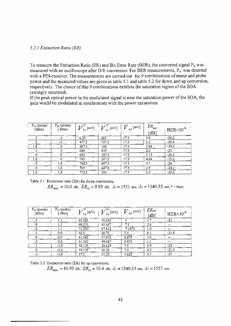
To measure the Extinction Ratio (ER) and Bit Error Rate (BER), the converted signal P2L wasmeasured with an oscilloscope after DIE conversion. For BER measurements, P2L was detectedwith a PIN-receiver. The measurements are carried out for 9 combinations of pump and probepower and the measured values are given in table 5.1 and table 5.2 for down and up conversion,respectively. The choice of this 9 combinations exhibits the saturation region of the SOA(strongly saturated).If the peak optical power in the modulated signal is near the saturation power of the SOA, thegain would be modulated in synchronism with the power excursions.
P IO (pump) P20 (probe) "I" "0"Vre/[mV] ERout[dBm] [ dBm] V 2L [mY] V 2L [mV]
rdBlBER<10-9
-3 -3 6.25 265 17.5 3.9 -24.20 -3 477.5 157.5 17.5 5.2 -24.4
1.8 -3 487.5 140 17.5 5.84 -24.5-3 0 680 435 17.5 2.0 -230 0 655 327.5 17.5 3.12 -24.1
1.8 0 745 267.5 17.5 4.64 -25.2-3 1.8 742.5 467.5 17.5 2.1 -200 1.8 785 447.5 17.5 2.5 -24.1
1.8 1.8 772.5 355 17.5 3.5 -25.2
Table 5.1 Extinction ratio (ER) for down conversion;
ERlaser =10.0 dB; ER10 =9.95 dB; Al =1551 nm; A2 =1540.53 nm; *=f1oor;
PIO (pump) P20 (probe) "1" "0"Vre/[mV] ERout
[dBm] [ dBm] V 2L [mY] V 2L [mY]rdBl BER<10-9
3 1.1 65.625 30.625 5 3.7 -21 I
0 1.1 69.375 43.437 7.5 2.4 ---3 I.l 71.250 57.812 7.1875 1.0 --3 0.0 62.5 28.75 7.5 4.1 -21.80 0.0 61.562 37.812 6.875 3.0 --
-3 0.0 61.562 49.687 6.875 1.1 --3 -3.0 58.125 20.625 7.5 5.9 -220 -3.0 58.125 26.25 7.5 4.3 -21.3
-3 -3.0 57.5 31.25 5.625 3.1 -21
Table 5.2 Extinction ratio (ER) for up conversion;
ERlaser =10.93 dB; ERlO = lOA dB; Al =1540.53 nm; A2 =1551 nm;
41
ERLaser is measured at the output of external modulator. ERIO is extinction ratio at the input ofthe SOA and ERout is extinction ratio at the output of the SOA (P2L). Vref is the reference level.Based on the values in those tables, the next figure presents the extinction ratio at the output ofthe SOA which is a function of the pump power for each given fixed probe power.
Er vs Pumppower (P10) for Down Comersion
15] + P20. -3dBm f-~--~--:-_·:--~--lf--~--14 L:J. P2Q=. OdBm -r--r--l---'---I--'--r--13 J( P20=1.6dBm .. .L ..... '- __ I I I __ J __ E __
12 --l---t---l--.,--.,--~--~--:---t--~--~--~--11 - -:- .. -:- .. -:- .. ~ - - ~ .... T .. -;- - -~- .. ~- - -: -i - ... ~ ..10 - _ 1- .... 1_ ... _I .... .J .... ~ __ J.. ..... ~ __ 1_ .. _I _ .I _ .. L ..
I I I I I I I I I , I IiIi' 9 "".-"".-" -t" .. , - .. , - .. r .. -+ .. -4r .. -I" .. -I .... , T ....~ B .... I.... _ 1_ ... _I .. _ .1 ..... .! _ .. t .. _ '_ ... _1_ .. J.......,1 __ J. .!. __~ I I I I I + 6 I I I I I
W 7 1- - -,- .. -I - ~ .. - ~ ..... l" - .. ~ .. -1- .. -I" .. -t ~ .. - ,. ..
6 :- - .. :- .. -: i" .. f .. -~ .... i- - ..:- .. -: .... -: ~ .... + ..
: =:;: =t: =~~ : ~~ : t==; =: ~ : =:= ==:= = ~ ==~ : = ~ ==3 .... 1_ .. _ 1_ .. .6... ....... .1 .... L .... I...... 1_ .. _I .... _I .... .! .... .!. ....
~ .. ..4. .. -1: .. -~- .. ~ - - ~ .. - : - -~ - -:- - -: .. - ~ - .. ~ - - ~ - -l , 1 til r 1 , 1 1 1
1 -".- - - 1- .. -, - - -I - - i .... I - - .- - - ,- - -1- - -I - - 'j .. - T - -
°-3~~.2-."'1--'0-"'--....2"---....3-4"---....5-6"-----'---'-B---'g-J10P10 [dBm]
(a)
Er VS Pumppower (P10) (or Up Con-..ersion
16r;:======~==:c;-..,..--,r-.....--r-......,..--,I"""J15 . ~ + P20:l:' -3 dBm I~ _'- _-L.. .. _ 1. __ J, __ .J - .. -' .. - -1- -
14 ~ P20 = 0 dBm __ ~ __ ~ __ ~ __ ~ _ .. ~ __ ~ ; __P20 = 1.1 dBm I 1 1 , I 1 1
13 I 1 I 1 - - 1- - - ~ - - ~ - - '-; - - -; .. - +- .. -, - -12 - .... - - ~ - - -t _ - -I'" - -1- ... - .... - - ~ - - .. - - ~ .. - ~ - - -t - - -,- -
11 - - ~ .. - ~ .. - -: - - -:- .. -:- - -:- - - ~ .. - ~ - -,- - +- --:- --:--10 _ .. J. __ J __ -' , 1 ,,- __ L.. __ 1. __ J, __ .J __ -, 1._
m 9 • - ; .. - ~ - - ~ - - -: .. - -;. - - ~ - - ~ - - ~ - - :; - - ~ .. - -: - - ~ -
ffi ~ =~: ==~ ==~= ==:= ==:= ==~ ==L =!= =~ ==~= =~ ~ =~= =6 ·-+--~---:---:·--:--+--:.... -£· .. t··{---:---:--5 • _ 1. __ .I __ -' _ • _I .... _+.. __ l.. __& _ .. 1. •• ~ __ .J _ • -' .. __ 1_ •
1 1 1 + 1 .& 1 , I 1 , 1
~ ~ ~f ~ t~ ~ ;~ ~ f ~ ~~ ~ ~f~ ~ ~ ~ ~ f ~ ~ 1~ ~ ~ ~ ~ ~ ~ ~ ~!~ ~• 1 I 1 I 1 , 1 1 1 I I
1 - - i - - i - - -,- - -,- - -.- - -1- - - i· - j". - j •• -1- - -1-" -1-·
~3.L---:'-2---....1-~0-"'----=-2-3~....4~~5r-~6--=-7-6~~9':-":'10·P10 [dBm]
(b)
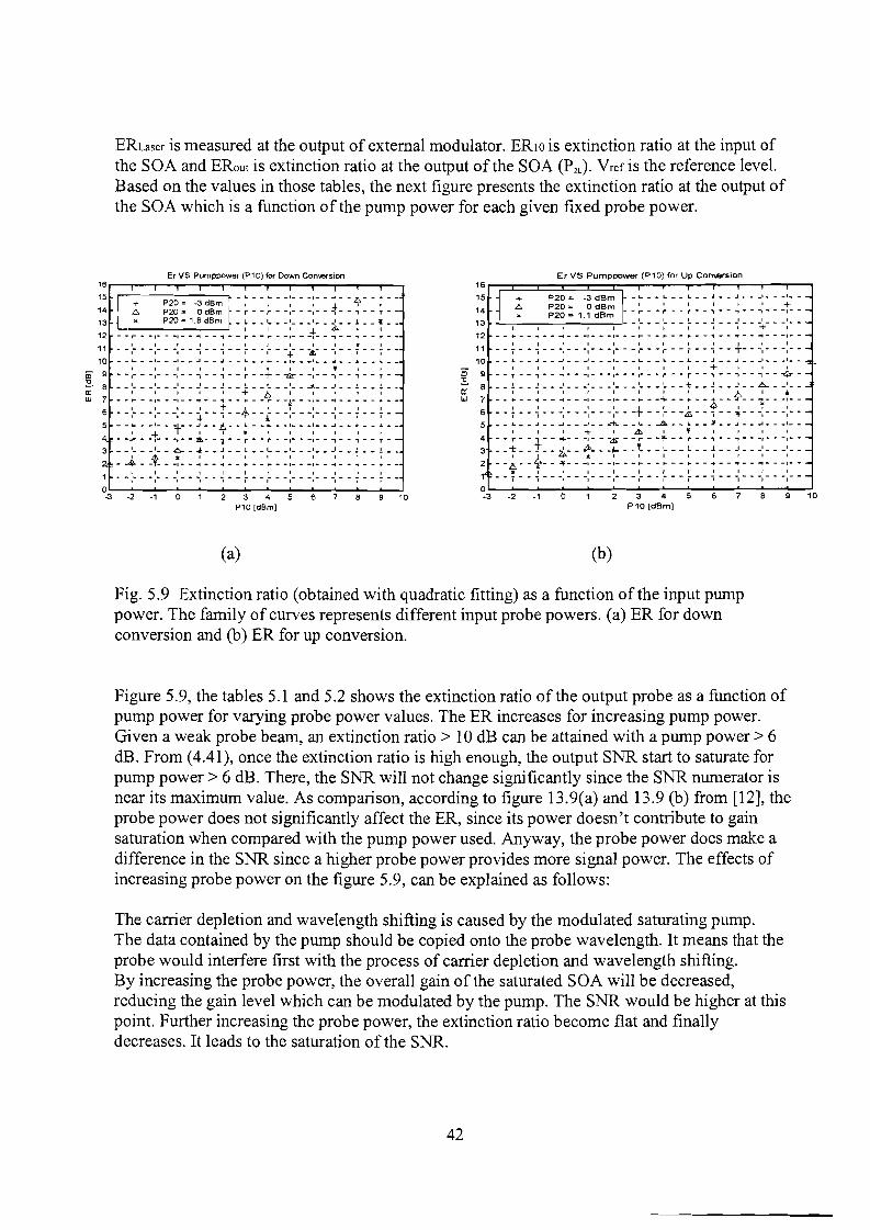
Fig. 5.9 Extinction ratio (obtained with quadratic fitting) as a function of the input pumppower. The family of curves represents different input probe powers. (a) ER for downconversion and (b) ER for up conversion.
Figure 5.9, the tables 5.1 and 5.2 shows the extinction ratio of the output probe as a function ofpump power for varying probe power values. The ER increases for increasing pump power.Given a weak probe beam, an extinction ratio> 10 dB can be attained with a pump power> 6dB. From (4.41), once the extinction ratio is high enough, the output SNR start to saturate forpump power> 6 dB. There, the SNR will not change significantly since the SNR numerator isnear its maximum value. As comparison, according to figure 13.9(a) and 13.9 (b) from [12], theprobe power does not significantly affect the ER, since its power doesn't contribute to gainsaturation when compared with the pump power used. Anyway, the probe power does make adifference in the SNR since a higher probe power provides more signal power. The effects ofincreasing probe power on the figure 5.9, can be explained as follows:
The carrier depletion and wavelength shifting is caused by the modulated saturating pump.The data contained by the pump should be copied onto the probe wavelength. It means that theprobe would interfere first with the process of carrier depletion and wavelength shifting.By increasing the probe power, the overall gain of the saturated SOA will be decreased,reducing the gain level which can be modulated by the pump. The SNR would be higher at thispoint. Further increasing the probe power, the extinction ratio become flat and finallydecreases. It leads to the saturation of the SNR.
42
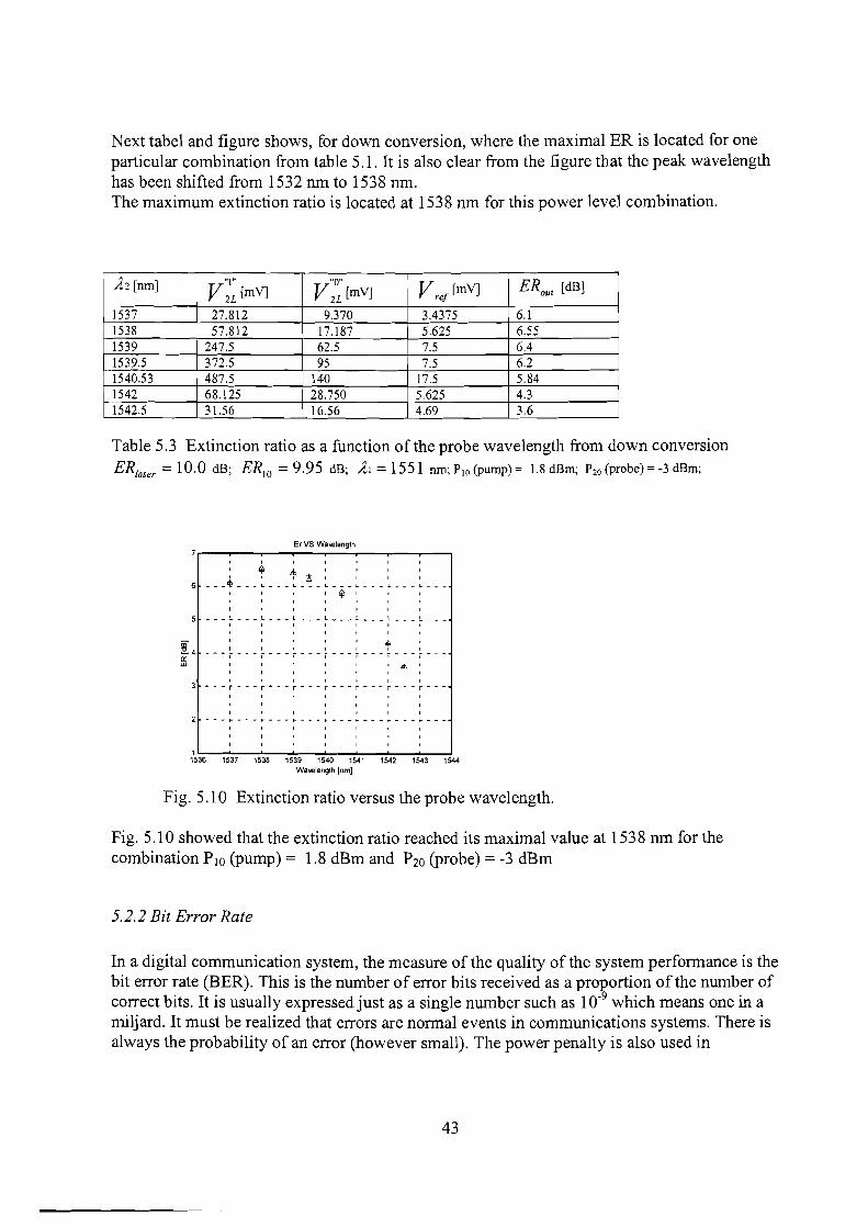
Next tabel and figure shows, for down conversion, where the maximal ER is located for oneparticular combination from table 5.1. It is also clear from the figure that the peak wavelengthhas been shifted from 1532 nm to 1538 nm.The maximum extinction ratio is located at 1538 nm for this power level combination.
,1.2 [nm] "111 "0" Vref [mY] ERau! [dB]V2L [mY] V2L [mY]
1537 27.812 9.370 3.4375 6.11538 57.812 17.187 5.625 6.551539 247.5 62.5 7.5 6.41539.5 372.5 95 7.5 6.21540.53 487.5 140 17.5 5.841542 68.125 28.750 5.625 4.31542.5 31.56 16.56 4.69 3.6
Table 5.3 Extinction ratio as a function of the probe wavelength from down conversionERJaser =10.0 dB; ERIO =9.95 dB; Al =1551 nm; PIO (pump) = 1.8 dBm; P20 (probe) =-3 dBm;
Er VS W.leiength
I 1 , •
I ~ !h I I 1 I
I I I! I I I I_ __ 4!, L L L L L L _
I I ¥ I, ,,
- __ !.. !.. !.. L !.. L 1. _I I I I I ,
~4 I + ,a::: ---i---'---.---j---I---)"---'---W I r I .dl. I, ,
I I • r I I r-- - r-- -r- --r- --r---r--- r- -- r---
,,
I I I I
2 ---"'---"'---"'---~---I----t----t----I I I \ I I I
'\'=36-:,7::53:"'"7---:-:'15:-::-38-:,7::539:--~154"""O~154~1"--'---54"""2 "--15""'43~1544Wawlength Inm]
Fig. 5.10 Extinction ratio versus the probe wavelength.
Fig. 5.10 showed that the extinction ratio reached its maximal value at 1538 nm for thecombination PIO (pump) = 1.8 dBm and Pzo (probe) = -3 dBm
5.2.2 Bit Error Rate
In a digital communication system, the measure of the quality of the system perfonnance is thebit error rate (BER). This is the number of error bits received as a pro~ortion of the number ofcorrect bits. It is usually expressed just as a single number such as 10- which means one in amiljard. It must be realized that errors are nonnal events in communications systems. There isalways the probability of an error (however small). The power penalty is also used in
43
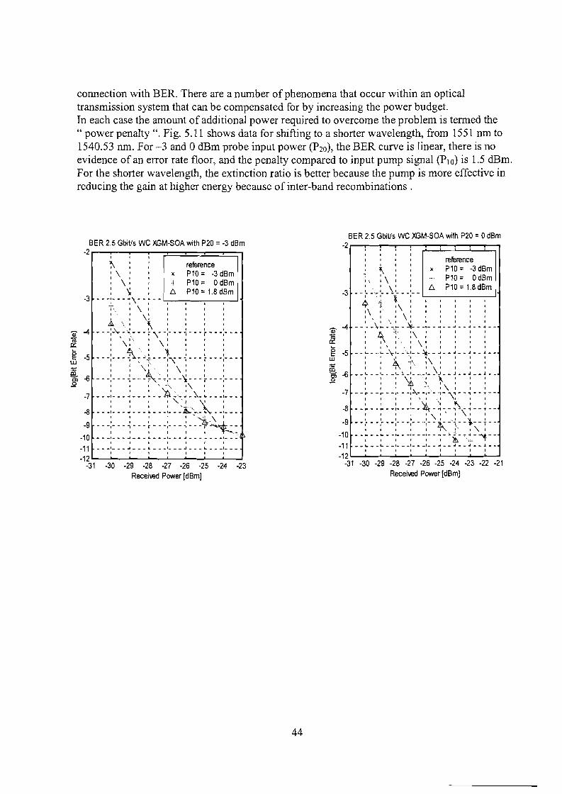
connection with BER. There are a number of phenomena that occur within an opticaltransmission system that can be compensated for by increasing the power budget.In each case the amount of additional power required to overcome the problem is termed the"power penalty". Fig. 5.11 shows data for shifting to a shorter wavelength, from 1551 run to1540.53 run. For -3 and 0 dBm probe input power (P20), the BER curve is linear, there is noevidence of an error rate floor, and the penalty compared to input pump signal (P IO) is 1.5 dBm.For the shorter wavelength, the extinction ratio is better because the pump is more effective inreducing the gain at higher energy because of inter-band recombinations.
BER 2.5 Gbitls we XGM-SOA with P20 = -3 dBm-2 r-i"'---;---;--;::~::::!:::::::::!::=:::!:==;"l
-30 -29 -28 -27 ·26 -25 -24 -23Receiwd Power [dBm]
referenceP10= -3dBmP10= OdBmP10 = 1.8 dBm
x
-28 -27 -26 -25 -24 -23 -22 -21Receiwd Power [dBm]
BER 2.5 Gbitls we XGM-SOA with P20 = 0 dBm
-2 rii,i""iii--;J:::::I:::::r=:I:::::::::::;l,I
I ~I>. I \ I I
- _:- ~,_:- _\:- - .:_. [j.I .. I 't " '-- ---'
.;. t ,..\ " ;\:I " • \ I I I I I I
.... ~... \ ~ .. -,:.... ~ - -: .. - ~ .... ~ .. - ~ --; --I ~ '1:' 1\' 1 • , 11 -:\ 1\ , , I 1 , 1
: :': \ : \: : : : :_ .. L- _ .' L- _\1__ '-~ ,_ .. ~__ ... __ .J _ .. ..I _ .. .I. .. _
, • '" I , 1 1 1
• I ~ -f'\, 1\ I 1 I 1
.... ~ .. _:- ... :- ~ _:- ..\_:- ~~ - .. ~ --~ --~ - ..I I 1 \1 ',1 ~ 1 1 1
: : ~ ~ ,~,\ :\: : :.. - ~ .. -r - -,.. - "I~- -,-': --r- ,., - -., ..... 'T --
I 1 1 I \. ,I \, 1 1
- -~ - .. ~ - .. :- .. _:- -~ -~-, .. ~ -~ -- ~ --I I I • I \. I" 1\1 I
1 1 I , ,'\ I ,,' "l 1- - .... - .. .- - -.- - -.- - .':- - ~- - " .. - "'- - j - -
I 1 I 1 , I"'-.}'" 1 '\ I
.. -~ .... ~ - -:- - -:- - -:- - ~ -.~- ~,..:,-~ --__ L- __ &... __ 1__ .. 1 1__ ... _ .. .J _ .. ..i .. _ .I. __
I I • , I , 1 • I
-8
-9
-10-11-12 L-.........--L_.l..--'----'_................---''---'-....I
-31 -30 -29
-3
CiJ -4iil0::
g -5LU
iii-6]I·7
referenceP10 = -3 dBmP10= OdBmP10= 1.8dBm
x~: \ :I \'
: ~ I
.. .. -;- .... ~ \ .... ~ - .. ~_.,......-.,_----.,._J 1
-; I \ I
I : \:
~ \: ~ : I---,-'..-'''':,.-----i\--.--- ---.---: '\:\' : \: :: 1\ \.: ~ :... .. -.- .... -. ~ -'·..r" .. -1\" .... -,- .....: : \ I',. : \ :
.. .. .. :_ .... ~ ......~ '2- ~:_ .... '\.. .. .. :I I I \ -~........, I \ I
I I I "", I •.. .. _1_ :Ti ' ~_ ~ _I ...
I I I I "\'1 \: I
.... _:- .... ~ ...... ~ .. .. _:.... -'~\.,- ~ .. _:- .. : : : ; :" 'i~" I
.. .. -.- , r -,- r -~~ .. -I , I I I I y ,~
.. .. _I ~ 1_ _I _I I I I I I I
.. .. _1_ .J &. 1 L _1_ .. _I I I I I I I
-3
CiJ -4iil0::
g -5w
!E. -6Ol.2
-7
-8
·9
-10-11-12
-31
44
BER 2.5 Gbit/s we XGM-SOA with P20 = 1.8 dBm-2 ....-~-r-"""'T"---y-,...-"'T"""--r~--,r--,..--,--,
referenceP10 = -3 dBmP10= OdBmP10 = 1.8 dBm
x
,,I
I,& I I : t
'\ } I I I.. _ I. ,; .. L.. .... 1_ .. _1_ .. -1- .... 6
I I I I ~
, \ I I , • \ l--~~~-_~-'1
I " I ) I I
f .,it.. I I I \'I ""'1"t I I I I I I I I I
I 1\, I I \1 I I I I I
.... :..... :- -\-:- .. -:- .. -:- .. ~_ .. -: .... ~ .... f .. -7"" +.. -I I \ I I I ,\ I I I , I
: : ~ .~ : :\: : : : :I I I \ I \ I '\ I I I I I
.... r .. ~. r .... .- 't: -,- ~ -1- .. ..,- .. i:::- .. ., .... 'T .... 'T .... r .. -I • I \ I \ I I \ I I I ,
: : : ~": : :,: ; : :............ '- .. .. 1_ .. _'\. .. ~~_ .. _' .... ~ .. \.J .... J. .... J. ..... .L .. _
: : : :\ :' : : ~ : : :, I ' I \ I I I I I ) I
.... ~ ~ ~ .. -1- .. \' __\_1_ ~ ~- ..
: : : : 4 ~~, : : ~ : :_.L. _L __ '__ .'•• _'~__' __ J •• J. _~_l_ .1._
I I , I I \ "''I I I ," I
I I , I I \' I , I *""" I.... ~ .... ~ .. -:- .. -:- .. ..~_ .. &" .. ~~~ .. ~ .... ~ .... ~ ..~~I I I I I I I' I I I I
.... r''''' r-" -,-" -,-" -,-" -,-"'" -"''',,-.'''' T"" T"" T"", I I I I I I ~, I I I
.... I- I- -I- .. -1- .. -1- -
I I , I I I ) I I I I
-8
-9
-10-11-12 L..-..a...-.........--'----'_"--..............--'-----I...............I.-...J
-31 -30 -29 -28 -27 -26 -25 -24 -23 -22 -21 -20 -19Recei~d Power [dBm]
-3
Q) -4roIX:'-e'- -5ill-iii0; -6.Q
-7
Pre! [dBm] BER
-30 l.OOe- 4-29 6.20e- 6-28 1.75e- 7-27 4.50e- 9-26 l.20e- 9-25 1.20e-IO
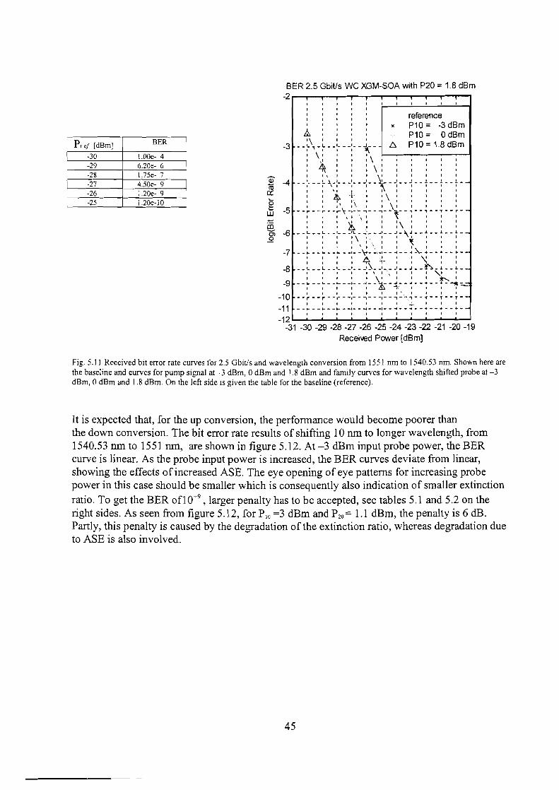
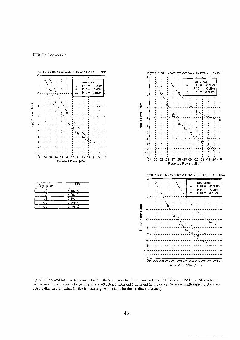
Fig. 5.11 Received bit error rate curves for 2.5 Gbit/s and wavelength conversion from 1551 nm to 1540.53 nm. Shown here arethe baseline and curves for pump signal at -3 dBm, 0 dBm and 1.8 dBm and family curves for wavelength shifted probe at-3dBm, 0 dBm and 1.8 dBm. On the left side is given the table for the baseline (reference).
It is expected that, for the up conversion, the performance would become poorer thanthe down conversion. The bit error rate results of shifting 10 run to longer wavelength, from1540.53 run to 1551 run, are shown in figure 5.12. At -3 dBm input probe power, the BERcurve is linear. As the probe input power is increased, the BER curves deviate from linear,showing the effects of increased ASE. The eye opening of eye patterns for increasing probepower in this case should be smaller which is consequently also indication of smaller extinctionratio. To get the BER of! 0-9
, larger penalty has to be accepted, see tables 5.1 and 5.2 on theright sides. As seen from figure 5.12, for P1G =3 dBm and P20 = 1.1 dBm, the penalty is 6 dB.Partly, this penalty is caused by the degradation ofthe extinction ratio, whereas degradation dueto ASE is also involved.
45
BER Up Conversion
BER 2.5 Gbit/s we XGM-SOA with P20 = -3 dBm-2 r-.....-;:-.--,..----..--,....-....---.--,..----..-....-...---,
referenceP10 = -3 dBmP10= OdBmP10= 3dBm
"
BER 2.5 Gbitls we XGM-SOA with P20 = 0 dBm
-21:-;-~;_;;========:;-1Lf :\ :'\ '\''\ : ~: 'i : : \~- -,- - "'.- - .. - -,- -~ L..._...,.._....,..._..,...._..,...._~
: :\: : : ':1 1\,,1 , 1 ~ I 1 1 I ,
1 1 "».. I 1 1 "I , 1 1 I
I 1 ~'" 1 I 1 ~' 1 1 1--:- - ~ --: \.~:- - ~ - - ~ --: ..~ .. -: --:- -~ ...I 1 1 \i", 1 I I :of ........ 1 1 I
I 1 I ~,. 1 I I I ..... 1 1
- _1- __'_ .. L _ .. _'l.\"i- _!. __ 1- - ~-- L_"":::'¥--.i:..-~ : : :~'.: : : : : 1
- _:..- ~- -~ .. _:- -~_'\.~,- .:- - ~ --~ -_:_ ... ~--, 1 1 I 1 ~ '<i~ I 1 I 1
1 1 1 1 1 ""T'\." I .... i I I 1
- -:- .. ~-- ~ - .. :- -~- - ~-~ "'~~,- --t,- -:- ... ~--- -:- - ~ -- ~ .. -:- -~ -.. ~ --:- :~- - ~;~ ;~ - ..
I I I I I 1 I I'" &. I ~+_ .. ' _ _ .J __ L _ .. "•• _ J _ .. 1. __ 1_ _ .J _ ~_ ... 1... _..J __
1 1 I 1 I I I I I ~ 1I 1 I 1 I I I I 1 , ..........
- -1-" -, _ .. j" - -.- - i - - i - -,-'" i" -;- - -.- - 6--__ 1 I __ 1. __ ,__ ~ __ 1 .. _1__ ..' .. _ !. __ 1 I __
• 1 1 , I I I 1 I 1 1
-8
-9
-10-11-12 L---'---'-_.L--'---'_-'----'-_'----'----'-_~
-31 -30 -29 -28 -27 -26 -25 -24 -23 -22 -21 -20 -19Receilled Power [dBm]
-3
ID10 -4a::g
lJ.J -5
iii0; -6E-
-7
referenceP10 = -3 dBmP10 = 0 dBmP10= 3dBm
"
~~,\ ~
,,,, , ,
~A ' : \: : :
_~'.!r_~ __ ~_~ __ ~: ,:\ :\: :: :~t \~ \ I
I I \, ~ " I I I I I I I
.. ~ .... ~ ~'''~ \ .. ~'\ ~ .... ~ .. ~ .. -:- .. ~ .. -:- .. ~ ..I I \ I 't I I I I I I
I I \ Jt I I I I I •
.. _' .... ~ ... ~ .. _.@,_ ! ~ .. I.... ! .. _'_ .. !.. .. _' .... !. ..I I I i \' '\ I I I I I: , I ~L I I I I I f
I I I I '\~ • I I I I I
.. ~ .... ~ .. ~ .... ~ ..~: ~ ~ .. -:- .. ~ .. -:- .. ~ ..I I I I I "4\ I'\. I 1 I I
.. _I .... l. .• .J .... '.... J .... 1_,,,, J., -'T"- .. 1 .. _1_ .. L ..I I I I I I <>:1\." I I I
I I I I I ~,~ I I I.. ~ ~ .. ~ ., .. ~ .. ~ .... ~ .. ~ -' t~) ....:.... : ......' l. .. J .... ,.... J .. _I.... J .... I .. "--""i::,~_ .. 1. ..
I I 1 I I I I I 4l;:::~ l' I
I t I I I I I I I l I.. -.... i .. -, .... 1- .. i .... ,- .. i .. -.- .. i .. ~- .. i ..
I I I I I I I I I I I.. "", .... i .. -......- .. ~ .....- ... i .... I'" .. j .. "'," - ;- ..
-9
-10
-11-12 L-.........--I._.......-'---'_..............._'-----'----'_..........J
-31 -30 -29 -28 -27 -26 -25 -24 -23 -22 -21 -20 -19
Receilled Power [dBm]
-3
ID -410a::~W -5
iii0; -6E-
-7
-8
1.1 dBm
referenceP10 = -3 dBmP10= OdBmP10 = 3 dBm
x
BER 2.5 Gbit/s we XGM-SOA with P20 =-2 ,-........-.---.--.....-..---.=========-,
4. \:~\ \: \'\1 :\ ~1 '~ , 1 1 \
- -:- - ;'\ - ~ - - ~ - -;_ ....j,......----------'-II I "', I 1 I 1 \ I 1 I I1 1 ~ 1 I 1 1 I 1 1 1
1 1 ~, I 1 1 ~ I • I 1
- -:- - -:- -'~ ~- ~ - -:- - ~- -~ ~ ~ - -:- -~ .. - ~ .. -I I 1 ''-''. I I 1 _ I I 1
, 1 , ~ .. , • , I" I 1 1
I 1 I?.. "" 1 I I I *-.1 1
.. -:.. - -: - - ~ - - i ~~~ '",- -: - - +- - :- - -: - , ..:- - +- -I IlL ....'-4" I 1 I ¥-..... I
1 1 I I .&." I''''~ -t' I 1 I .....__ 1......... __ .. __ ,," __1__ ..-1 __ '-ol .~" __ 1 __ -, __ .. __
• 1 1 II.&... t'<-.-.; ~ 1 I
1 1 1 I 1 I .... ~ I...,· ... +- 1 I
- -:- - -; .. - ~ - -IL
- -:- -~ .. -~: -2s, - ::~'~-'i-"~ --I I I I I I......... 1 • -;"
- .. 1- _ -I - - 4 •• - ~ - -1- _ ~ - .... - - ~ ........... -a - - .. - -1 1 1 I 1 I 1 I 1 - -J I--:- .. -:- .. ~ .. -~ --:- --;- -~ .... ~ .. -:- .. * .. ~ --
- -:- - -: ... - ~ - - ~ .. -;- - -: .. - 7- -:- ... -:- - -: - - +- -__ I.... _I_ .. .! __ !.. __ 1 ' __ J. __ 1 1_ .. -, __ .!. __
I I , I I 1 1 I 1 1 I
-30 -29 -28 -27 -26 -25 -24 -23 -22 -21 -20 -19Receilled Power [dBm)
-3
ID~ -4a::~g
lJ.J -5
iiiC; -6E-
-7
-8
-9
-10-11-12
-31
Pre! [dBm] BER
-30 4.10e-6-29 4.00e- 7-28 2.10e- 8-27 1.24e- 9-26 1.40e-lO
Fig. 5.12 Received bit errorrate curves for 2.5 Gbit/s and wavelength conversion from 1540.53 nm to 1551 nm. Shown hereare the baseline and curves for pump signal at -3 dBm, 0 dBm and 3 dBm and family curves for wavelength shifted probe at-3dBm, 0 dBm and 1.1 dBm. On the left side is given the table for the baseline (reference).
46
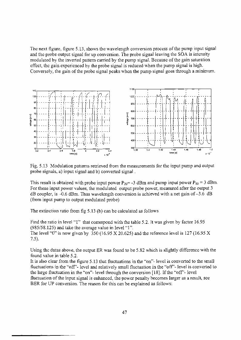
The next figure, figure 5.13, shows the wavelength conversion process of the pump input signaland the probe output signal for up conversion. The probe signal leaving the SOA is intensitymodulated by the inverted pattern carried by the pump signal. Because of the gain saturationeffect, the gain experienced by the probe signal is reduced when the pump signal is high.Conversely, the gain of the probe signal peaks when the pump signal goes through a minimum.
·7X 10
,,r- .. - ....,,
.. lo- .. _ ..
,__l __ ~_
,
,,,,
.. -."
,.. -,_.. -
300 L-_-'--_---'-__-'-_--'-__'-------l
1.38 1.4 1.42 1.44 1.46 1.46 1.5time [s]
900 ---- ,--,
500 --------
400 -----,-,,
1100,-----,------,---r----,----r----,
,1000 - - - - - ,- - - -
5" 800 _ .. - .. -:- .. -
E :i 700 -----.---..'§
600
I... _
,
,-1- - ..
-(-{
i ....,
,, -
,-----1-
20 t !.._, ~: v:., -~--10L-_""-,-_..=:-_---'-,----_-'--_~ __
3.2 3.4 3.6 3.8 4.2 4.4time [5] x 10-8
110,--.....,.--;:;--.----r----...,....----.-----,
100 -----:( --~---- :--I--~:--I I I I
I , I t
90 - - - - - - - - -.. - - - t. - - - - _, ,, ,
80 - - - - - - - - f 1- - - - - - -
, , ,5' 70 - - - - : - - - - ~ t_ - - - - ' -
E , ,i 60 - - - - 1- - - - - .. - 1- .. - - - -
~ I950 ---- l-----j
,40 I L
, ,, ,
30 ---- 1-----,..- .., ,
Fig. 5.13 Modulation patterns retrieved from the measurements for the input pump and outputprobe signals, a) input signal and b) converted signal.
This result is obtained with probe input power Pzo= -3 dBm and pump input power PIO = 3 dBm.For these input power values, the modulated output probe power, measured after the output 3dB coupler, is -0.6 dBm. Thus wavelength conversion is achieved with a net gain of-3.6 dB(from input pump to output modulated probe)
The extinction ratio from fig 5.13 (b) can be calculated as follows
Find the ratio in level "I" that correspond with the table 5.2. It was given by factor 16.95(985/58.125) and take the average value in level "I".The level "0" is now given by 350 (16.95 X 20.625) and the reference level is 127 (16.95 X7.5).
Using the datas above, the output ER was found to be 5.82 which is slightly difference with thefound value in table 5.2.It is also clear from the figure 5.13 that fluctuations in the "on"- level is converted to the smallfluctuations in the "off'- level and relatively small fluctuation in the "off'- level is converted tothe large fluctuation in the "on"- level through the conversion [18]. If the "off'- levelfluctuation of the input signal is enhanced, the power penalty becomes larger as a result, seeBER for UP conversion. The reason for this can be explained as follows:
47

If a zero bit is represented by a finite power level rather than a true complete absence ofpower,then the difference between the power level of 1 bit and that of a 0 bit will be decreased. Thepower level of the 0 bit becomes the noise floor of every 1 bit. The receiver decision point hasto be adjusted to a higherJevel and therefore there is an increased probability of an error. Thiscan be compensated for by an increase in available power level at the receiver.
48
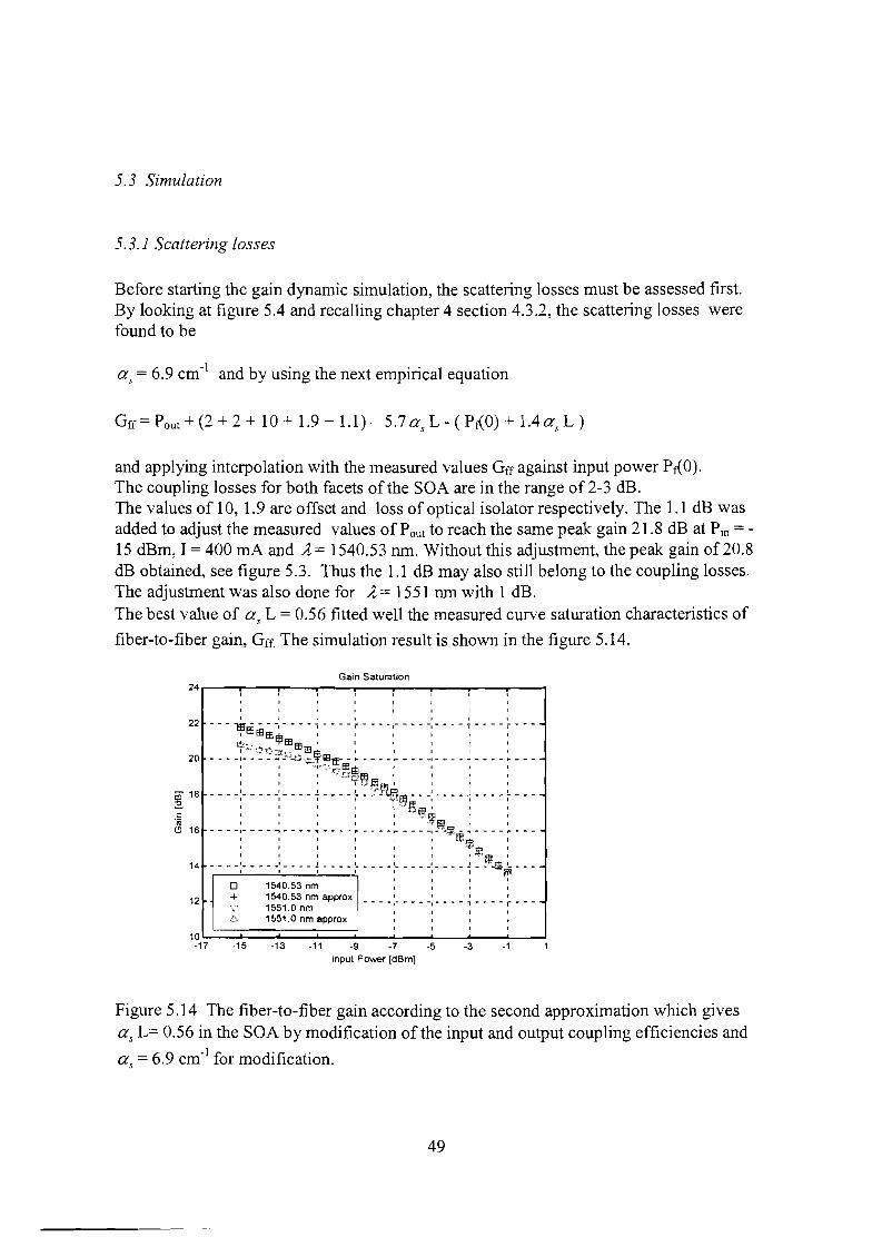
5.3 Simulation
5.3.1 Scattering losses
Before starting the gain dynamic simulation, the scattering losses must be assessed first.By looking at figure 5.4 and recalling chapter 4 section 4.3.2, the scattering losses werefound to be
as = 6.9 cm-] and by using the next empirical equation
Gff = Pout + (2 + 2 + 10 + 1.9 + 1.1) - 5.7 as L - (PiO) + 1.4 as L)
and applying interpolation with the measured values Gff against input power PiO).The coupling losses for both facets of the SOA are in the range of 2-3 dB.The values of 10, 1.9 are offset and loss of optical isolator respectively. The 1.1 dB wasadded to adjust the measured values of Pout to reach the same peak gain 21.8 dB at Pin =
15 dBm, I = 400 rnA and ..-1.= 1540.53 nm. Without this adjustment, the peak gain of20.8dB obtained, see figure 5.3. Thus the 1.1 dB may also still belong to the coupling losses.The adjustment was also done for ..-1. = 1551 nm with 1 dB.The best value of as L = 0.56 fitted well the measured curve saturation characteristics of
fiber-to-fiber gain, Gff. The simulation result is shown in the figure 5.14.
Gain Saturation24.---..---....--....--........--r---r--......--......--'"
-1-3
o+12
,22 - - - 1ir _.. __I - - - - ~ _ - - - '.......... 1- _ .. __' .... __ ~ .... __ '- .... _
~ ffiE8ffi~ : : : : : :
20 - - - ~1~·="~~~·1~L!~:~~~~~ ----i- --- -! - - - - ~ - - - - ~ - . -: : - ~J,~T~ IE: : : :
.. - - _1- ...... _, _ .. _ .. ..!. ........ I.... '~'~!..ea£5 .. .. _I _ ...... J ........ !.. _ .. _: : ; : ~('~,~~~. : : :I I I I I ~,o.~'33 r I
I I I I I J,',~'.'-S3 I I
.... - -,- ...... ..., ........ '" ........ ~ - - .. -,- .. - .. -, -''''''~... "'I .. - - - ~ .. - -
I I I I vm_~ I
I I I I I I ~;f:~ P.:!' I
I I I I , r I ~lm: I
14 .. - .. - '...... - _I _ .... _ .! ........ I.- .. _ .... I.. _ .. __I _ .... _ .!. .... :.m L. ......I I I I I I I 'ffl
, "1540.53nm ""1540.53 nm approx '•• _ • _' ~ ~ _
1551.0nm :: t I
1551.0 nm approx, "
L=::::&:=::;:=:::;:=::::i._-':'"_-.:.._~'_""":"_.-J10-17 -15 -13 -11 -9 -7 -5
Input Power [dBm]
r:'ffic.9 16
OJ 18:2.
Figure 5.14 The fiber-to-fiber gain according to the second approximation which givesas L= 0.56 in the SOA by modification of the input and output coupling efficiencies and
as = 6.9 cm-] for modification.
49
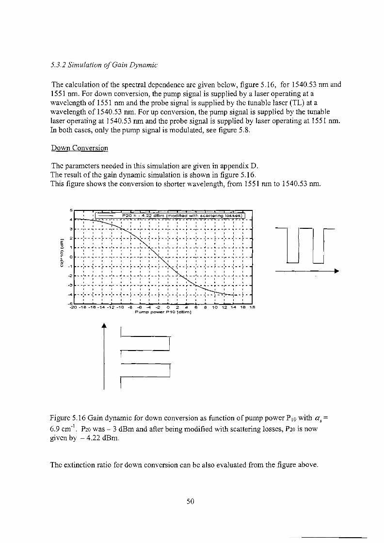
5.3.2 Simulation ofGain Dynamic
The calculation of the spectral dependence are given below, figure 5.16, for 1540.53 nm and1551 nm. For down conversion, the pump signal is supplied by a laser operating at awavelength of 1551 nm and the probe signal is supplied by the tunable laser (TL) at awavelength of 1540.53 nm. For up conversion, the pump signal is supplied by the tunablelaser operating at 1540.53 nm and the probe signal is supplied by laser operating at 1551 nm.In both cases, only the pump signal is modulated, see figure 5.8.
Down Conversion
The parameters needed in this simulation are given in appendix D.The result of the gain dynamic simulation is shown in figure 5.16.This figure shows the conversion to shorter wavelength, from 1551 nm to 1540.53 nm.
5 r,....-~::J:::::::::::I:::::t:::::~:::I:::::;:!;=.::t=:::r:~::;::::I:=::I~r:=I:=~::J::::::::::t;'"".,P20 = - 4.22 dBm (modified with scattering losses)
4 - -- ---- -- ••• - -- ---- •• ---- -- -I I I I 1 I I I I I I I I ,
1 I I I I I I I I I I I I I I I3 - -,- .. ., - ... ,.. ... -1- ... ... r ... -,- ... ., ...... I'" ... -,- ... ., ...... r ... -,- ... ., ...... r ... -,- ... ., ..... r ...
I I I I I I I I I I I I I
~ 2 --:--->·-r--:--~--i-- I--~--i---: .. -~--r----~--i_--:--~--i_-UJ I I I I I I I I I I I I I I I I
~ , _1_ 1_ L _1_.. .. L .. _1_ L _I L _1_ L ..
a ::: I I : : I :::::::::
r a ... -1- ... ., ..... ,.. ... -1- .. ., ...... ,.. .. -,- ... ., ...... ... -,- .. ., ..... ,.. .. -,- ... ., ...... r ... -,_ .. ., ..... r ...Q. 'I I
(3 -1 ... -: ..... ~"''';'",,,,,,,,,, ~ ...... i- ... -:- .. ~ ...... i- ... -, .. -: ..... r'" -;_ ... ~ ...... r'" -:..... ~ ..... r'"I I I I I I I I I 'I I I I I I
-2 _I .J L. 1 L .. _I _I oJ _ L 1_ L ...I I I I I I I I I I I • I I I I I
I I I I I I I I 1 I 1 I I I I I I-3 - -I- - 1 - - r .. -.- - 1 - .. r - -,- ... ., .... r - -."'" .. 1 - ... r - - - 1 - - r .. -,- .. ., - - r ..
I I 1 I I I • I I I I 1 I' I I
-4 - -:- - ~ - - r .. ---~ --i- .. -:- .. ~ - ... r--:- ... -: --r--:- -~ -... i - ... : - r-I I I I 'I I I 1 I I I 1 I I
-~2·I:'O--1:".:8:---:1':-6--1~4--"::"12:'""":-1"::O~-8--6~_4.....~-2:--0~~2......4......~6~8:--:1"::O~12:--!14~1~6--:'18Pump power P10 IdBm)
-U-lr
Figure 5.16 Gain dynamic for down conversion as function of pump power P IO with as =
6.9 em-I. PZO was - 3 dBm and after being modified with scattering losses, Pzo is nowgiven by - 4.22 dBm.
The extinction ratio for down conversion can be also evaluated from the figure above.
50
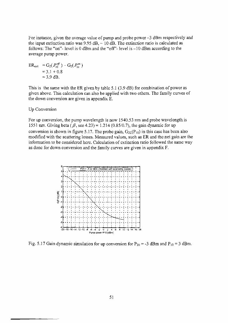
4
For instance, given the average value of pump and probe power -3 dBm respectively andthe input extinction ratio was 9.95 dB, ~ 10 dB. The extinction ratio is calculated asfollows: The "on"-level is 0 dBm and the "off'-level is -10 dBm according to theaverage pump power.
ERou( = G2( ~t )- G2( ~~n )
=3.1 +0.8= 3.9 dB.
This is the same with the ER given by table 5.1 (3.9 dB) for combination of power asgiven above. This calculation can also be applied with two others. The family curves ofthe down conversion are given in appendix E.
Up Conversion
For up conversion, the pump wavelength is now 1540.53 nm and probe wavelength is1551 nm. Giving beta (fl, see 4.23) = 1.214 (0.85/0.7), the gain dynamic for up
conversion is shown in figure 5.17. The probe gain, G2L(P IO) in this case has been alsomodified with the scattering losses. Measured values, such as ER and the net gain are theinformation to be considered here. Calculation of extinction ratio followed the same wayas done for down conversion and the family curves are given in appendix F.
6 r-'''i''''''===:~=:=;~~:=::::I::===7''==::Z:=o::::::''''-', - P20 = -4.22 dBm (modified with scattering losses) ,5 -!..-------------------------------!.-
I I I I I I I I I I I I I I I I I I
I I I I I I • I I I I I , I I I I I.. r- - r- - ,- .. ,- - ,- ... ,- -, .. -, - -, .. ., - ., .. ., .. ., ... , .. "T - T .. T -
I I I I I I I I , I I I I I I I
3 .. 1.. .. L too _ ,_ .. '__ , __ ' __' __ , __1 __I .. oJ .. oJ .. .J .. .J ... J .. .1 .. l _
I 1 I I I I I I I I I I I I I I I
I I , 1 I I I I I I I I , I I I , I
2 .. r ... r ... ,-" .. ,- -.- -,- -,'" -, - -,'" -, .. -. .. , - , .. , .. , ... T .. T -
I I I I I I I I I I r I I I I I , I
en" 1 ...... - L. - ... ... 1_.. _1 __ 1__ 1__I ... _I ... ~ _ ..J ... ..I .. ..I .. ..I .. ,J .. J,. ... ,j. _
:::. I I • I I , I I I I J I I I I , I I
~ 0 -r-:--:--:--:--, -:--:--:--:--;.-:-~-~-~-1-~-~-Q.. I I I I I I I I I I I , I I I I ICJ -1 .. ~ .. ~ .. r- .. 1- -1- - 1_ -1- _1 __1__I _ ...... o.l _ -l .. ..a .. -l - -4 ... + .. + -
r I , I I t I "I'" I , I ,
-2 ' I I , I , , , , , J , I r I , I I- i - ,- -,- -,- -,- -,- -,- -,- - -,. -,- -,- j - ~ - -; - ~ - j --;-I , , , I , , I , , , I I , , I , ,
·3 - r- - ~ - r- - ,- - ,- - ,- - ,- -, - -, - -, .., - ., - ., - "T - , - , - T - T -
, I , • , I • , 'I '" I , , I
-4 _ L _ L • '__ 1__ '_ ... '__ '. _' __I __, __, _
I , , I , , , , , , , I I I"
, I , r I I I , , , , I , , , , I ,
-5 - r - r ... \- - ,- - ,- - ,- ... ,- -, - -, - -\ - -,'" , - , - , - , - , - T ... T -, I , • , , I , , , I , , , I , I I
-6 ........-..&........-'-...........r.-...................--'-.......-'-...........r.-.................--'--1-20 -18 -16 -14 -12 -10 ~ -6 -4 -2 0 2 4 6 8 10 12 14 16 18
Pump power P10 IdBm]
Fig. 5.17 Gain dynamic simulation for up conversion for P20 = -3 dBm and PIO = 3 dBm.
51
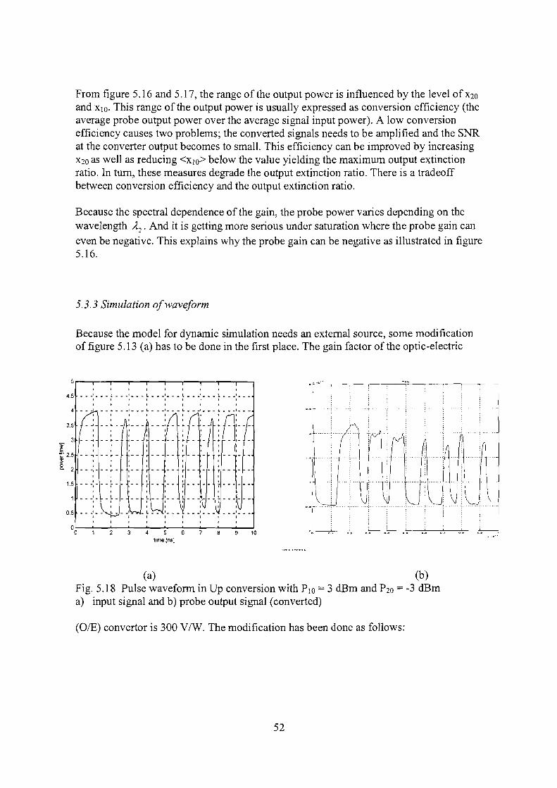
From figure 5.16 and 5.17, the range of the output power is influenced by the level of xzoand XIO. This range of the output power is usually expressed as conversion efficiency (theaverage probe output power over the average signal input power). A low conversionefficiency causes two problems; the converted signals needs to be amplified and the SNRat the converter output becomes to small. This efficiency can be improved by increasingXzo as well as reducing <XIO> below the value yielding the maximum output extinctionratio. In tum, these measures degrade the output extinction ratio. There is a tradeoffbetween conversion efficiency and the output extinction ratio.
Because the spectral dependence of the gain, the probe power varies depending on thewavelength A,. And it is getting more serious under saturation where the probe gain can
even be negative. This explains why the probe gain can be negative as illustrated in figure5.16.
5.3.3 Simulation ofwaveform
Because the model for dynamic simulation needs an external source, some modificationof figure 5.13 (a) has to be done in the first place. The gain factor of the optic-electric
00'-----'--2'"---3'--.........4 - .....5 - ....6 - ....7 --'--.........9 ---'10
lime/ns]
, ,1 I .. _L L __ ' __ , 1 _
0.5 - - .: - ~ ~.I __~_ ~ ~: ~ :~ __~ :~ __I --p I I I I , , I
I I I , I I I I I
"0 ,
i (~,
( rv rV( l........
....... .... ti \• \J\~ \J .\- "-- U
i0 o. o.
,,r" - .. ...
,-------,
,,r ..... ...
, ,, , ,
---,---r- .--,1.5 ---:---;.-
4.5 .... _1 ....... .!.. .... _I ..... _ ~ .. .. _' ........ !.. .. __' ........ !. ........ _ .....I I I I I I I
I I I I I I I
4 -/1- -~ ---: ---~ ---:-~- ~ (--: ---~ r-- -:- -f-3.5 f -~ ---~ --j :- - -f. ---;f - ~ - :-1 ~ -:---
3 .... ~ ... - ~ ... :..... I I ~ .. :.. ~ ... :_ ...
" ,, ,I~ 25
~ 2
w ~Fig. 5.18 Pulse waveform in Up conversion with P IO = 3 dBm and Pzo = -3 dBma) input signal and b) probe output signal (converted)
(OlE) convertor is 300 V/W. The modification has been done as follows:
52
The input extinction ratio was lOA dB where y 1= 125 mY, yO = 15.625 mY and Yref =4.687 mY. Divide y 1= 125 mY, yO = 15.625 mY and Yref= 4.687 mY with factor 300and then multiplied with factor 10. The power P for each levels are given by p 1 = 4.17mW, pO = 0.52 mW and Pref = 0.156 mW. From these power values, there are anagreement between the transformed voltage (Y) levels, now is Power (P), and figure 5.18.The factor lOis the read factor imposed by the oscilloscope read out. The equation (4.7)from chapter 4 can be written in the form as given below
This is the non-linear differential equation of the 1sl order.To solve this, the differential gains and also the carrier transparency for each wavelengthmust be known first.
The internal saturation power of the amplifier is given by
p"SGt = - 8 dBm = 0.2 mW (for 1551 nm)
P2SjGt =-7 dBm = 0.16 mW (for 1540.53 nm)
L= 800 Jim; w = 1.8 Jim; d = 0.1 Jim; [= 0.2; is = 0.2 nsec.
gNl = 2.885 10-20 and gNZ = 3.606 10-20;
The carrier transparencies can be calculated as follows:
Using the unsaturated gain equation G =exp([gi(N)L) and linear gain coefficient- -
equationgi(N,A) =gM{A)[N - NOi(A)] , the N01 and N02 can be found where
N = Ir;/(eV).
The used current I is not the maximal allowed current in the SOA, but it is the currentwhere the unsaturated gain almost remains in the equal niveau (transparent) at the givencurrent. For sake of clarity, see again figure 5.2. That figure shows the distribution of thegain against the wavelength. The 200 rnA current shows nearly tranparency of interestedwavelength interval (1530 nm - 1560 nm). From simulation with programMatlab/Simulink (appendix H), it has been found that 1= 100 rnA.
The modified external input pump signal is now injected in the model and the results ofthis dynamic simulation is shown in figure 5.18 (b).
53
Chapter 6
Conclusions and Recommendations
The perfonnance of a cross gain modulated wavelength converter (WC) was examined byits extinction ratio.In chapter 5 is shown how the extinction ratio can be found. This was achieved in twoways:
• from measurement and• from dynamic gain simulation according to [9].
Measurement:
If a zero bit is represented by a finite power level rather than a true complete absence ofpower, then the difference between the power level of "1" bit and that ofa "0" bit isdecreased. The power level of the 0 bit becomes the noise floor of every 1 bit. Thereceiver decision point has to be higher and therefore there is an increased power penalty.This can be compensated by an increase in available power level at the receiver. An ERof 10 dB incurs a power penalty of about 1 dB. An ER of 3 dB causes a power penalty of5 dB.To make a transition from 1551 nm to 1540.53 nm or 1540.53 nm to 1551, a WC needs ahigh pump power to saturate further the gain while the probe power should remaine muchmore smaller than the pump power (power dependence). Higher pump power provideshigher gain saturation and extinction ratio but doesn't affect the SNR much since theextinction ratio was already near its maximum. The maximal obtained extinction ratiowas - 6 dB for both cases, up and down conversion. This is actually still low in order toget better perfonnance of the wavelength conversion. If the ER was higher than 6 dB,translation from 1540.53 nm to 1535 nm can be made possible, for instance by placingthe second converter. The wavelength 1535 nm is the lowest wavelength from KPN.Translation to a higher wavelength gave always extinction ratio degradation. The powerpenalty for down conversion was about 1.5 dB and for up conversion 5 dB. This higherpenalty is caused by 1) amplified spontaneous emission (ASE) noise originating in thecounter propagating direction, at the end of the SOA (L), as confinned in [17,18], 2) thepolarization dependence (;::; 2 dB) of the SOA gave some contribution in the penalty.These conclusions are valid when the SOA is driven with maximal current, I = 400 rnA.
54
It is may be in the future become a task to see the performance of this we withusing two EDFAs (increasing the pump) at the transmitter side to obtain higher gainsaturation andsmaller currents (1< 400 rnA).
In the last case, the saturation output power can be higher for longer wavelength whichwas in this project actually being the case. The longest wavelength is 1560 nm (lOP)which is so far from the peak wavelength of the SOA (1533 nm for drive current 1=400nm). It has been shown in section 5.1 that the saturation (probe) output power is alsowavelength dependent. Decreasing the drive current, consequently, the net gain alsowould be decreased (current dependent). But the saturation output power would beincreased ( for shorter and longer wavelength ), see figure 5.5 (b). With this argument,the extinction ratio would be increased. It has influence on the gradient of the gain curvewhere the ER can be determined.
Simulation:
The model presented here has shown its capability to predict the performance of thecross-gain modulated (XGM) based on the Semiconductor Optical Amplifier. It was alsoshown in this model how the scattering losses can be taken into consideration bymodified coupling efficiencies. The simulation output extinction ratio shown reasonableagreement with the measured values. The error tolerancy of this model was in the interval0- 1.3 dB. Also, the carrier lifetime in this simulation has been considered constant.
The quality of any received signal in this experiment, in the future, can also be translatedin term of signal-to-noise ratio or SNR by using the equation 4.41.The ER was already known. Only the spontaneous emission factor was still remainunclear but for the bulk SOA, the spontaneous emission factor may be assumed to havevalue between 1 and 1.5. According to [12], this emission factor also depends on thewavelength and should also give different values for different pump power levels ("0"and "1 " bits)
Further, this model gives an easy perspective to study the dynamic response of theconverter that governed by the effective carrier lifetime as describe in chapter 4 equation4.21. All the needed parameters can be calculated after the spectrals dependence ag,
- -bg and the unsaturated gains G1 and G2 are defined. Also, the transmission of the probeand signal intensity noise can be derived from this model [9].
The pulse waveform from figure 5.18 (b) has the same form as the average carrier densitybecause the exponential dependency (4.8) and always inverted from its input waveform.The risetime pulse ensured that the pulse dispersion could not be observed.
55

Acknowledgments
I wish to thank everyone who helped me to achieve the results are presented in thisreport.
My special thank to Eduward Tangdiongga for help with the system measurements andhelpful discussion.
Buug de Waard is gratefully acknowledged for infonnative discussions andencouragement.
Finally, my great thank to professor Khoe for his pennission to do my graduation projectat the division Electro-optical Communication and he is always there for an advice andencouragement.
56
Appendix A.ISubstituting (4.5) into (4.4) and using the power equation in the form as given by
dPi = r gi(N) Pi(Z)dz
[I L Jd - fN(t,z)dz
L L 0 == Ll~_ N _ L rgi(N)Pi(Z)lJzdt ~leV rs i=I,2 Ahc/Ai r
L
frgi(N)Pi(Z)dZ
L dNav(t) - LN L lIT "" 0rs - - IVav- L.. rs...::..------dt i=I,2 Ahc/Ai
L
fdPi(Z)
- "" 0=LN - LNav - L.. ------::.-----i=1,2rgi(N)Ahc/Ai r rsgi(N)
Ts dNav(t) == N _ Nav _ L xi(L) - Xi(O) ,dt i=I,2 rgNlL
(A1.I)
(A1.2)
the rate of carrier density is now transformed into the average carrier density, as given by (Al.2).
57
Appendix A.2Large-Signal Analysis For Co-Propagation
For large-signal analysis with i=1,2, the equation (4.7) in stationary and using the equation (4.10)(4.12) for large-signal can be written as
_ - (XIL - XIO) (X2L - X20)0- N - Nav- -fgN,L fgN2L
or
- (XIL - X10) l( Xu - X20)N =Nav+ + .
fgNIL fgN2L
The above equation can be written also in term ofNm as given by
With (4.9), this equation is transformed as follows
and multiplied both side with fgN2L yields the following equation
Xu gNI - -It has been defined that - = G2, jJ= - and Gi =exp(fg,{N)L.
X20 gN2
58
(A.2.I)
(A.2.2)
(A.2.3)
Modification of (A.2.2) with those definitions above gives
or
Then, written the equation (A.2.I) in term of NO! as
and multiplied both side with fgN,L yields the following equation
Working out this equation with the same definitions as done before yields
or
Substitution of (A.2A) into (A.2.6) gives
59
(A.2A)
(A.2.6)
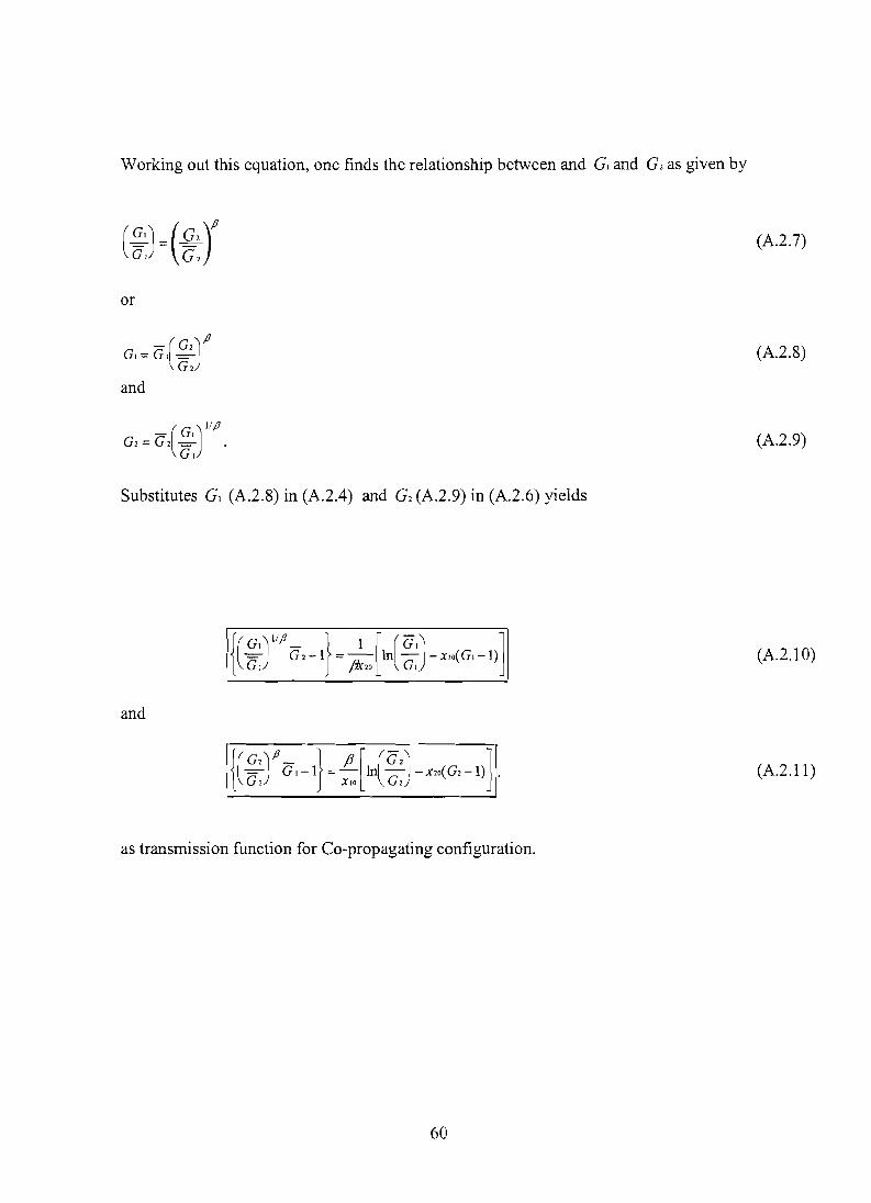
Working out this equation, one finds the relationship between and G, and G2 as given by
or
- (G,]fJGl= Gl G~
and
Substitutes G, (A.2.S) in (A2A) and G2 (A.2.9) in (A2.6) yields
and
as transmission function for Co-propagating configuration.
60
(A2.?)
(A2.8)
(A2.9)
(A2.10)
(A2.11)
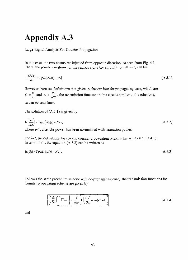
Appendix A.3Large-Signal Analysis For Counter-Propagation
In this case, the two beams are injected from opposite direction, as seen from Fig. 4.1.There, the power variations for the signals along the amplifier length is given by
However from the definitions that given in chapter four for propagating case, which are
G, =~ and XIL =~, the ransmission function in this case is similar to the other one,XIL p
lsat
as can be seen later.
The solution of (A.3.1) is given by
In(~) = rgNL[ Nav(t) - No;],XIL
where i=l, after the power has been normalized with saturation power.
For i=2, the definitions for co- and counter propagating remains the same (see Fig.4.1)In term of Gi, the equation (A.3.2) can be written as
In(G,) = rgNlL[ Nav(t) - N 01] .
(A.3.1)
(A.3.2)
(A.3.3)
Follows the same procedure as done with co-propagating case, the transmission functions forCounter propagating scheme are given by
and
61
(A.3.4)

62
(A.3.5)
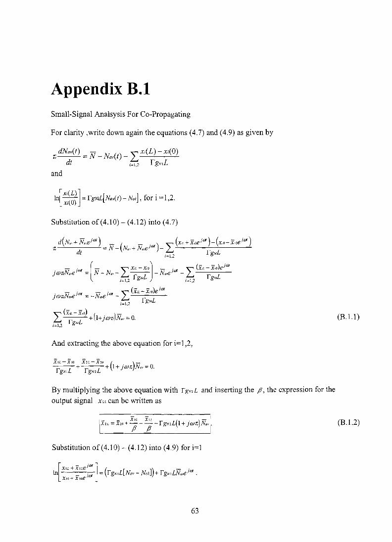
Appendix B.ISmall-Signal Analsysis For Co-Propagating
For clarity ,write down again the equations (4.7) and (4.9) as given by
dNav(t) _ N _ N. ( ) _ "xi(L) - Xi(O)r; - avt L..J
dt i=1,2 rgN,Land
[Xi(L)] [ ].In Xi(O) =0 rgNiL Nav(t) - Noi , fOrI = 1,2.
Substitution of (4.1 0) - (4.12) into (4.7)
And extracting the above equation for i=l,2,
By multiplying the above equation with rgv2 L and inserting the j3, the expression for the
output signal X2L can be written as
- - X 10 XlL L(') ;::;X2L =0 X20 + - - - - rgN2 1+ j(ur; lVav •
j3 j3
Substitution of (4.10) - (4.12) into (4.9) for i=1
63
(B.I.l)
(B.1.2)
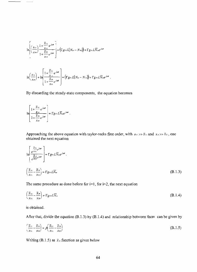
By discarding the steady-state components, the equation becomes
Approaching the above equation with taylor-reeks first order, with XlL» XIL and XIO» XIO , oneobtained the next equation
(XIL XIO) ---- =rgNlLNa,XIL XIO
The same procedure as done before for i=l, for i=2, the next equation
is obtained.
(B.1.3)
(RIA)
After that, divide the equation (B.1.3) by (RIA) and relationship between them can be given by
(XIL _ XIO) = j Xu _ X20)
XIL XIO p~ Xu X20
Writing (B.I.5) as XIL function as given below
64
(B.I.5)
- XIL - fJXlL - fJ XlL -XlL =-XlO+ -X2L- -X20
XIO X2L X20
Inserting (B.l.4) and (B.1.6) into the (B.1.2), gives
XIO 1 [XIL XIL XI[] ( )_X2L = X20+-
fJ-fJ -XIO+j3-X2L-j3-X20 -fgN2L 1+ j(j)'li No,
XIO X2L X20
_ _ XlO 1 XIL _ XlL _ XIL _ (.)-X2L = X20+----XIQ--X2L+-X2o-fgN2L 1+ J(j)'li No,
fJ fJ XIO Xu X20
_ _ XIO 1 GlXlO _ G,XlO _ GIXIO _ [gmL ( . )[X2L X20]X2L = X20+-----X10---X2L+--X20--- 1+ J(j)T, ---
fJ fJ XIQ G2X20 X20 [gN2L X2L X20
_ GlXIO _ (1 + j(j)z;) _ _ GlXIQ _ ( . ) X20 XIQ 1 G,XIQ_X2L+--X2L+ X2L = X'O+--X20+ 1+ J(j)'li -+-----XIO
G2X20 G2X20 X20 X20 j3 j3 XIQ
__ G[1+ j (j)Z;+X20+GIXIQ] XIO G [ G,-1 ]X2L=X20 2 -- 2X20 --------
1+ j (j)r; + G1XlQ + G2X20 fJ 1+ j (j)r; + GlXIQ + G2X20
The first and second bracket on the right side of the equation are coefficients which canbe expressed by
(B.1.6)
(B.1.7)
and
(B.1.8)
(B.1.9)
where OJB is the 3 dB bandwidth and given by
1+ GlXlO + G2X20aJn = -------1
65
(B. 1.10)

Thus, (B .1.7) can be written in tenns of its coefficient and presented by next equation
66
(B.1. I I)
Apendix B.2Small-Signal Analsysis For Counter-Propagating
For counter propagating, only for i=l, the equation (4.7) and (4.9) needs modification.
According to the definitions from chapter four,
XIO d PIOGI=-an XIL=--,XIL ~sat
the equation (4,7) and (4.9) becomes
r; dNav(t) = N _ Nav(t) _ Xl(O) - xl(L) _ xz(L) - xz(O)dt r gN,L r gNzL
and
[XI(O)] [ ]In -- =rgNIL Nav(t) - NOl ,xl(L)
for i =1.
Following the same procedure as in case of co-propagating, in the first stage nextequation would be found as
The second stage is to find the relationship as given below
(XIO XIL) _r LAT--- - gNI iVa",
XIO X,L
The expression for the input signal can be expressed as follows
67
(B.2.I)
(B.2.2)
(B.2.3)
- X,L - fJ X1L - fJXIL -X,L ==-XIO+ -XU- -X20
XID Xu X'D
by doing comparison from (B.2.2) and (B.2.3).
By substituting (B.2A) in (B.2.!), the output Xu can be expressed as
where
and
And the 3 dB bandwidth, COB, is given by
OJ, == -----r;
68
(B.2A)
(B.2.S)
(B.2.6)
(B.2.7)
(B.2.8)
Appendix C
If X20 = 0 and using the definitions in chapter 4, the equation (B.1.6) can be written as
XIL = G,+XIO+ jJ~G2b(m)X1OXu
Inserting the b(m) from (B.1.9) in (C.l) gives
- - [G f.Y:: XIO ( (GI -1)x2o/jJJ]-XIL - 1+ jJV'- - ( .) XIOX20 OJB + } m r;
Rewriting the equation (B.1.II) in case of X20 = 0,
69
(C.I)
(Co2)
(C.3)
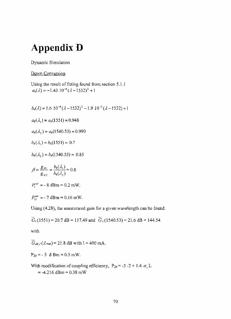
Appendix DDynamic Simulation
Down Conversion
Using the result of fitting found from section 5.1.1Qg("z) = -1.43 10-4("z -1532)2 + 1
Qg(A,) = Qg(1551) =0.948
~sat =_8 dBm = 0.2 mW.
Using (4.28), the unsaturated gain for a given wavelength can be found.
Gl (1551) = 20.7 dB = 117.49 and G2 (1540.53) = 21.6 dB = 144.54
with
G dB,! ("z max) = 21.8 dB with I = 400 rnA.
P20 = - 3 d Bm = 0.5 mW.
With modification of coupling efficiency, P20 = -3 -2 + 1.4 as L
= -4.216 dBm = 0.38 mW
70
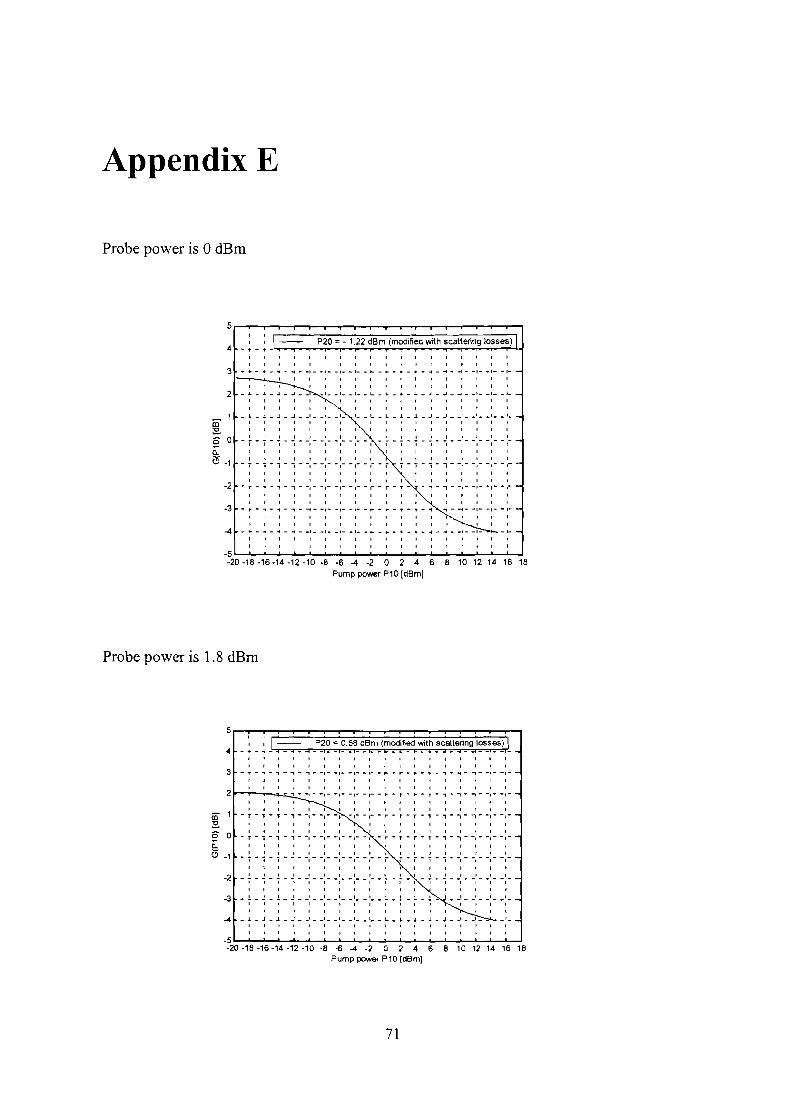
2
iii::!.S 0
~ -1
-2
-3
-4
Appendix E
Probe power is 0 dBm
,• P20 = - 1.22 dBm (modified with scattering losses)
4 -. - , - ......-r-......-,,-..,..--.-..,....--,-'-..,.......,.-...--......-..---;;;.....--r'-L-4, ,I I I I I I I I , I I I t I I I I
3 - ... - ........ - -I" -1- -1- _1 __ 1_ ... ~ _ ........ _ ...... -l _ ...... _1_ -1- _1 __ 1_
I-~_'--'I I I I I 'I I I ,
I I I I I I I 'I I I I2 ... &. ... .l .. .l ... ..J ...... _1 __ 1__ 1_ ... L. .. L _ &. ... J. .......... ..I __1 __ 1__ 1__ I.
I I I I I I I I , I I 1 I
I I I l I I I I I
... J. .. J ... J ... J ... _' .. _1 __ '_ ,- .. L .. L. ... J. .. 1 ... J ... J .. _I .. _' __ '_ ... I.I I I I I I I I I I I I I I I I I
I I I I I I I
I I I I J I I I I I I I I... i .. i i .. i - -, ,." I 'i .. i - "i .. -I I-
I J I I I
I I I J I I I I I I I I... T .. , , i - -,'" -,- -1- .. ,- ,- i 'i'" i .. 1 ,- -
J I I I I I I I
I I I I 1 I I I I I I I I I I I
·2 .. T .. ., - "T .. ., .. -." -,- -,. "'.- ... r .. r ... T" .. '1 ... ., .. "," .,. -,- ... ,- -
I I l I I \ I I I I I I
I I I I I I I' I I I I I \
·3 -1'-'-"-"-""--'--'--'--"'-"'-1'-T-1 "-""--'--1--'-I J I I I I I I I I
I I I I I I I I I
-4 -I - -1- _1 __ I.. _ ~ _ _ + _ + .. oj .. ~ __I· _I_
I I I t I I I 1 I I I, , ,-5 1...-........1...-..1...-...1.-->-........................................---"---"--'_'--...............1...-............
-20 -18 -16 -14 -12 -10 -8 -6 -4 -2 0 2 4 6 8 10 12 14 16 18Pump power P10 [dBm]
Probe power is 1.8 dBm
Jo-"""-'--~-:..:1,... ..., - -1- -1- -,- -1- - ... - r - ... - T -, -., - -1- -1- -1-,I I I I I I I I I I , I I 1 I I , 1
- T -, -, -, - -,- -1- -, -1- -1- - r - r - T -, -, - -. - -1- -1- -,'"
I I I' 1 I I 1 • I ( •
I I I I I I I I I I I I 1 • I , , I- T - , - , - , - -I - -1- -1- ·1- - I - r - r - r • T .. , - -. - -1- -. - -,-
• I I I I I' I ., I I
I I 1 I I' I I I I 1 1 I 1... i- j- i - .,- -.--.- -1-- - -.- -i i - i -; -j- -.--.--.---
I' •• I I' 1 1 I
I I • I I' , 1 I I I I I I •- j - i .. i - -, - -I - -I - - - - 1- - 1- - 1- • i-I - i ... i - -I - -I - - - - -
I I' I I
.. .!.. _.!. _.!. __I __, __'_ .. 1__ 1__ 1__ '- ... !.. _!. _.!. _ '. _1 __' .. _1_ .. I_
I • I I J I \ I I I , I I I" I
1 I I \ I I , I ., t 1 ,
_,1._ J _J _J .. _1 __I. _' __ 1__ I.. _L_ L _.1.l_J _ J_ .1 ,_I I , I I 1 'I I 1 I I I' I I
I I I I I I
-5 i:-:'::--:'::--:':-:'::--:.......~~..................-'-......-'-"""-"""-...I.-...I.-~-20 -18 -16 -14 -12 -10 -8 -6 -4 -2 0 2 4 6 8 10 12 14 16 18
Pump powe. P10 {dBm]
71
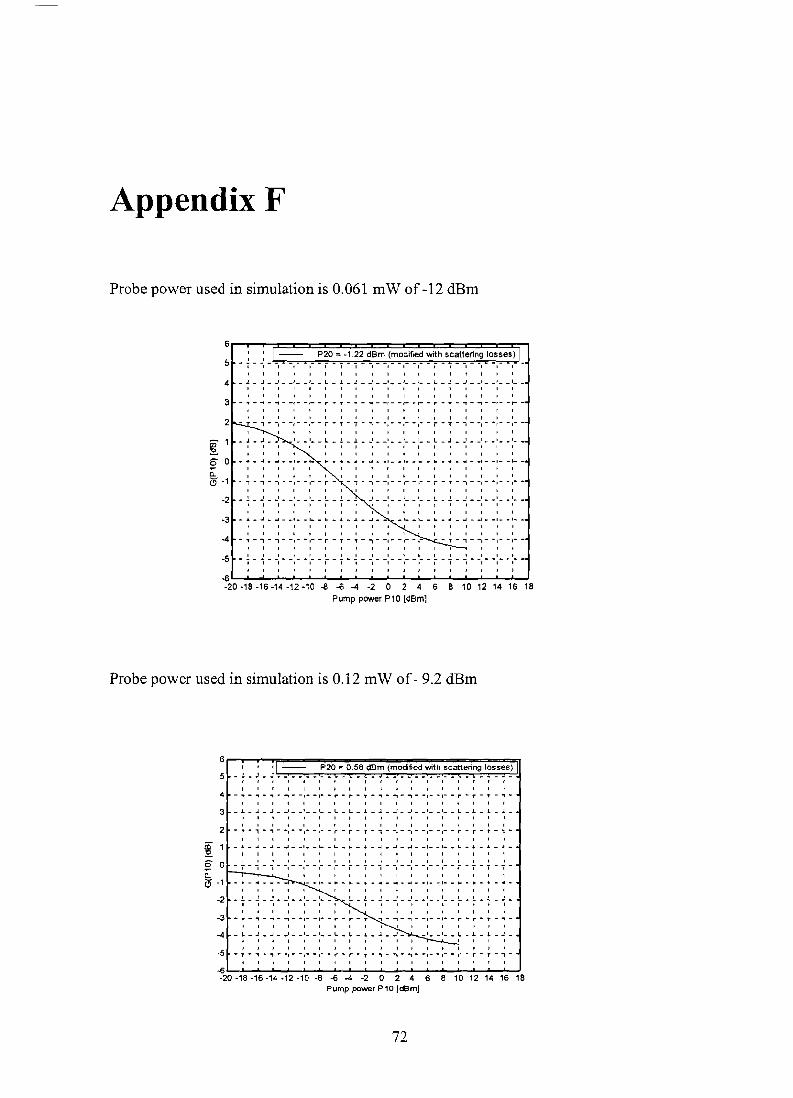
Appendix F
Probe power used in simulation is 0.061 mW of -12 dBm
P20 = ., .22 dBm (modified with scattering losses), ,- i - -," -.- -,- -1-""" i'" i" -,- -,- -,- -,-'" i" i" -," -,- "'," -1-"
I I I I I I I I I I I I I t I I
.. J. .. j .. .J .. _, __ '.... L .. J. .. J .. .J ..... __ ,__ ,_ .. L .. .J. .. ,J .. _' ... _' .. _1_ ..I I I I I I I I I I I I I I I
I I I I I
.. l' .......... ... -, ..... ,- .. ~ ....... l' ..... .. -r" ... ,- .. t- .. ~ ............ -. .. -, .... .- ..,I I I , , I I I I I , I I I I I I
.. , .. -. - -,- -.- .. r .. T - T .. -, ... -," ... ,- .. I'"' .. r ... T - , ... -," -,- ".- ...I I I I I I I I I I
1_ ... I..... l .. ! ... J. ... _' ... _' ..... 1_ .. I.... L .. J. .. ..J .. _I .. _I .... '....I I I I , I I I , I I I I I
I I I I I I I I I I I I
........ ..1 .. ..1 .. _1 __ 1_ ~ _1_ .. 1_ .. ~ ~ ..I .. _1 __ 1__ 1_ ..
I I t I
I I I I I I I I I I I I I I I I I
... T ... ., - -, ... -,- "'.- .. r'" ... T - ., .. -." "'.- .. ,- .. r ... T ... i .. -." -.- "'.- ..I I I I t I I I
.. .!. ... .! ... _' .. _1_ .. '.... L ... ! .... _' .. _' ..... I.... '.... L. .. ! .. .! ... _' .. _1_ ... '....I I I I I I I I I I I I I I ,
I 'I I I I I
..... ..I ..... __I .... 1_ .. "" ........ ..I ..... .. 1_ .. l- .. ~ ...... ..I .. _I .. _1_ ... I.....
I I I I
I I I I I I I t 1
.. T ... i .. -. .. -.- ".- .. r .. T .. T .. i .. -." ".- .. I-I I I I I I I I I I I
I I I I r I I I I I I I I I I I I I.. i .. -, ... -I" ....... ,- .. i .. i ... i .. -.... -,- -.- ".- .. i .. i .. i ... -." ....... ," -
I I I I I I I I I I I
_6 .......................-'-..............................--' '--..........-'-"""--L..-'--'-........--I-20 ·18 -16 -14 -12 ·10 -a -6 -4 -2 0 2 4 6 8 10 12 14 16 18
Pump power P10 [dBm]
6
5
4
3
2
CD~
S 00..<3' -1
·2
·3
-4
·5
Probe power used in simulation is 0.12 mW of-9.2 dBm
6
5
4
3
2
iii':Eo
~ 0c..<3' -1
-2
-3
-4
-5
,-- P20; 0.58 dBm (modified with scattenng losses)_.!._..!_J .. _ ..... ... ........... __ ...
" '" II
.. T" ., .. ., ... .., ... -,- -,- .. r" ... r .. T .. ., .. .., .. .., .. -,- -,- .. r .. T .. T ... ., ...
I I I I I I I I I I' j I
.. L .. J .. J ... _I .. _' __ '..... L .. L ... L ... J .. -J ... _' .. _I ..... '......... J. .. L ... J ...I I I I I I I I • I I I I I I I I I
I I I I I I I I I I I I I I I I I I.. T" , ... , ... -," -1- -,- .. r ~ r .. T .. , .. -I" "," -,- -,- .. r .. T .. T .. , ...
I 1 I I I I I I I I I I
..... .I .. ~ .. ...... _I .. _I.... L. .. ~ ...... -l .. ..I .. J .. _1_ ... 1_ .. L. ...... J. .. .I ..,I I I I I I I I I I I I I I
-i-,-,-~----l--r-r-T-'-~--I----l--r-T-i-'-
I I I I
,_~_!_~_J_J '__ L_l_l_J ..
I I t I I I I I I I
I I I I I I I
.. T""""""'- -,- -,_ .. r" po .. ,. ., .. .,- -1- -,- -,_ ... r" .... r - T -.,-
" ,_ L _ J _ oJ __I __ 1__ I.., _ ..... L _ .L ... J _ .J _
I 1 I 1 1
I I I 1 , I I , I I I I I I I , I 1
- T - , .. ., - -. - -.- "'1- .. r ... r - T ... ., - ... - -, - -.- - 1- - r ... T - T - , ...
I 1 I I 1 • • I 1 I I 1 • 1 , I I
-6 ...........................-'--'---"--'L..--L-..............-'-.........--"......_L-.L-............-'-20 ·18 -16 -14 -12 ·10 -8 -6 -4 ·2 0 2 4 6 8 10 12 14 16 18
Pump power P10 [dBm]
72
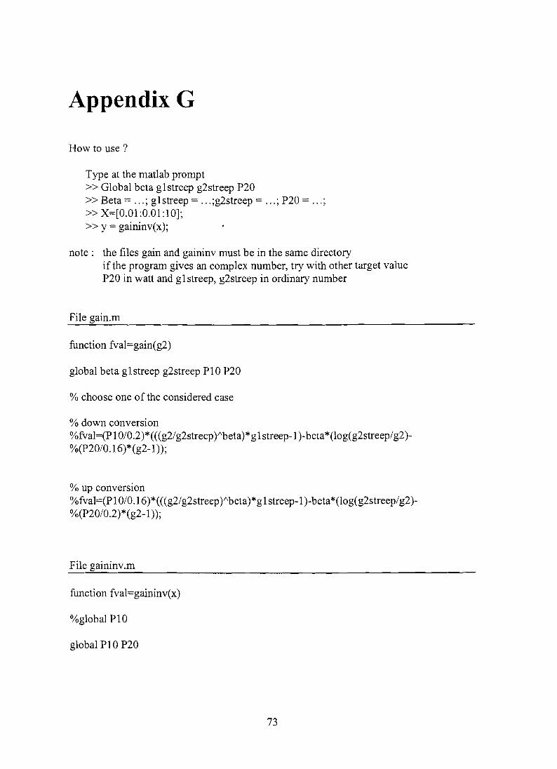
Appendix G
How to use?
Type at the matlab prompt» Global beta glstreep g2streep P20»Beta = ... ; glstreep = ... ;g2streep = ... ; P20 = ... ;» X=[O.Ol:O.Ol:IO];»y = gaininv(x);
note: the files gain and gaininv must be in the same directoryif the program gives an complex number, try with other target valueP20 in watt and gI streep, g2streep in ordinary number
File gain.m
function fval=gain(g2)
global beta glstreep g2streep PIO P20
% choose one of the considered case
% down conversion%fval=(P I0/0.2)*(((g2/g2streep)"'beta)*g I streep-l )-beta*(log(g2streep/g2)%(P20/0.16)*(g2-1 ));
% up conversion%fval=(P I0/0. I6)*(((g2/g2streep)"'beta)*g I streep-l )-beta*(log(g2streep/g2)%(P20/O.2)*(g2-1 ));
File gaininv.m
function fval=gaininv(x)
%global PIO
global PIO P20
73
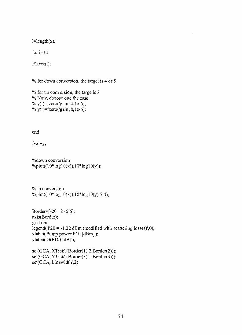
l=length(x);
fori=I:1
PI0=x(i);
% for down conversion, the target is 4 or 5
% for up conversion, the targe is 8% Now, choose one the case% y(i)=fzero('gain',4, 1e-6);% y(i)=fzero('gain',8, 1e-6);
end
fval=y;
%down conversion%plot((1 O*logl O(x)),1O*logl O(y));
%up conversion%plot((1 O*log1O(x)),1O*logl 0(y)-7.4);
Border=[-20 18 -6 6];axis(Border);grid on;legend('P20 = -1.22 dBm (modified with scattering losses)',O);xlabel('Pump power PI 0 [dBm]');ylabel('G(P10) [dB]');
set(GCA,'XTick',(Border(I):2:Border(2)));set(GCA,'YTick',(Border(3): 1:Border(4)));set(GCA,'Linewidth',2)
74
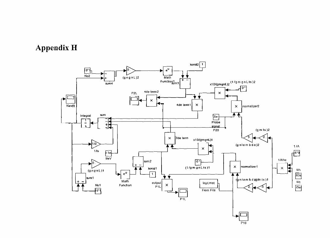
Appendix H
X nonnalizer2
x
x1 O/(gmgnL)2 (1 /g m 9 n L ts )2
0'
4de term 1 X
4de term2P2L
sum4
~-No2.--_...c..::.__+l.+
BNav(t)
1/A(g n Ia m b d a )2
X nonnalizer1
x
0'1------1
x10/(gmgnL)1
(1/g m 9 n LIs )1
X 3de term
BP1L
.1e
lIeV
1/ts
1--------I~1/0.,>---1
P10

Appendix I
76
Bibliography
[1] "Special Issue on Optical Amplifiers," J. Ligthwave Technol., vol. 9, no. 2, Feb1991.
[2] D.M. Braun and R.1. Jungerrnan, "Ultra-low reflectivity 1.5 j.I m Semiconductor
Laser Preamplifier," Optics Lett, vol. 20. Pp 1154-1156, Apr. 1995.
[3] A.J. Collar, G.D. Henshall, J. Farre, B. Mikkelsen, Z. Wang, L. Eskildsen, D.S.Olesen, and K.E. Stubkjaer, "Low Residual Reflectivity of Angled-FacetSemiconductor Laser Amplifiers," IEEE Photonics Technol. Lett., vol. 2, pp.553-555, Aug. 1990.
[4] 1. Cha, M. Kitamura, and 1. Mito, "1.5 pm Band Traveling Wave Semiconductor
Optical Amplifiers with Window Facet Structure," Electron. Lett., vol. 25, pp.242-243, Feb. 1989.
[5] M.K.L. Max, "Principles and Applications of Optical Communication," chapter17, pp. 865-867, 1996.
[6] N.A. Olsson, M.G. Oberg, L.D. Tzeng, and T. Cella, "Ultra-low Reflectivity 1.5pm Semiconductor Laser Preamplifier," Electron. Lett, vol. 24, pp. 569-570,
Apr. 1988.
[7] M. J. O'Mahony, et aI., in Conference on Optical Fiber Communication Tech.Digest, Atlanta, 1986, paper WE5.
[8] K. E. Stubkjaer et aI., "Optical Wavelngth Converters," in Proc. ofECOC '94,Firenze, Hally, vol. 2, pp. 635-642, September 1994.
[9] K. Obermann, S. Kindt, D. Breuer and K. Petermann, "Performance Analysis ofWavelength Converters Based on Cross-Gain Modulation in SemiconductorOptical Amplifiers," J. Lightwave Technol., vol. 16, no. 1, January 1998.
[10] K. E. Stubkjaer et aI., "Semiconductor Optical Amplifier as Linear Amplfiers,Gates and Wavelength Converters," TuC5.1, pp. 60-66.
[11] T. Durhuus et aI., "All-Optical Wavelength Conversion by Semiconductor OpticalAmplfiers," J. Lightwave Technol., vol. 14, pp.942-953, June 1996.
77
[12] A. E. Willner and W. Shief, "Optimal Spectral and Power parameters for allwavelength shifting: Single stage, fanout, and cascadability," J. LightwaveTechnol., vo1.13, pp. 771-781,1995.
[13] D. Marcenac and A. Mecozzi, " Switches and Frequency Converters Based onCross-Gain Modulation in Semiconductor Optical Amplifiers," IEEE Photon.Technol. Lett., vol. 9, pp. 749-751, June 1997.
[14] A. Mecozzi, "Small-Signal Theory of Wavelength Converters Based on CrossGain Modulation in Semiconductor Optical Amplifiers," IEEE Photon. Technol.Lett., vol. 8, pp. 1471-1473, November 1996.
[16] 1.M. Wiesenfeld et aI., "Wavelength Conversion at 10 Gb/s using aSemiconductor Optical Amplifier," IEEE Photon. Technol. Lett., vol. 5, no. 11,November 1993.
[17] K. Obermann and et aI., Noise Characteristic of Semiconductor-OpticalAmplifiers Used for Wavelength Conversion via Cross-Gain and Cross-PhaseModulation," IEEE Photon. Technol. Lett., vol. 9, pp. 312-314, March 1997.
[18] K. Inoue, "Noise Transfer Characteristics in Wavelength Convertion Based onCross-Gain Saturation in Semiconductor Optical Amplifier," IEEE Photon.Technol. Lett., vol. 8, pp. 888-890, July 1996.
[19] S. Chelles et aI., "Extinction Ratio of Cross-Gain Modulated MultistageWavelength Converters: Model and Experiments," IEEE Photon. Technol. Lett.,vol. 9, pp. 758-760, June 1997.
[20] 1. M. Wiesenfel, "Wavelength Conversion Techniques," in Proc. OFC '96, SanJose, Ca, Feb. 1996, pp. 71-72, paper TuP 1.
[21] M. Fujiwara et aI., "A coherent Photonic Wavelength Division Switching systemfor broadband networks," in Proc. ECOC "8, Brighton, U.K., Sept. 1988, pp. 139142.
[22] S. J. B. Yoo, "Wavelength Conversion Tehnologies for WDM networkapplications," J. Lightwave Technol., vol. 14, pp. 955-966, June 1996.
[23] R. W. Tkach et aI., "Four-Photon mixing and high-speed WDM systems," 1.Lightwave Technol., vol. 13, pp. 841-849, May 1995.
[24] 1. Zhou et aI., "Four wave mixing wavelength conversion efficiency insemiconductor traveling-wave amplifiers measured to 65-nm of wavelengthshift," IEEE Photon. Technol. Lett., vol. 6, pp. 984-987, Aug. 1994.
78

[25] D. Marcenac, "Travelling wave effects for wavelength conversion by cross gainand cross phase modulation in optical amplifiers," lnt. J. Optoelecetron., vol. lO,no.5,pp. 325-329,1995.
[26] D. A. O. Davies, " Small-Signal Analysis of Wavelength Conversion inSemiconductor Laser Amplifiers via Gain Saturation," IEEE Photon. Technol.Lett., vol. 7, no. 6, pp. 617-619, June 1995.
[27] D. Marcenac et aI., "Bandwidth enhancement of wavelength conversion viacross-gain modulation by semiconductor optical maplifier cascade," Elec. Lett.,vol. 31, no. 17, pp. 1442-1443,17 Augustus 1995.
79