Embed Size (px)
Citation preview
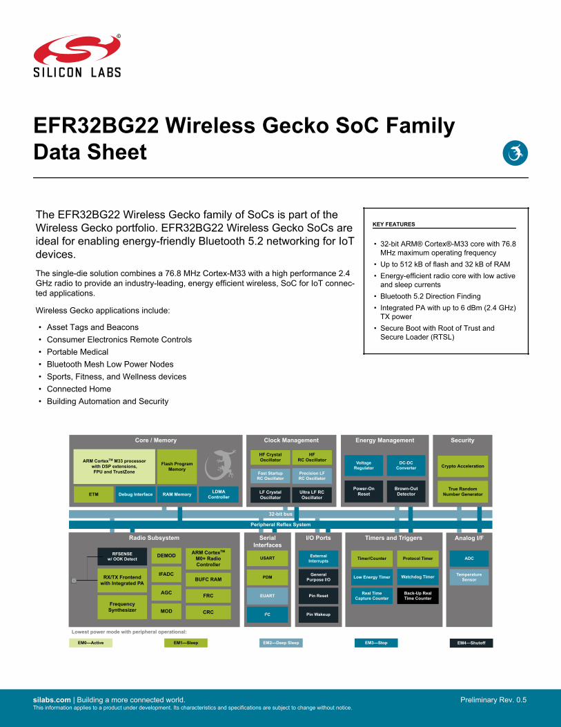
EFR32BG22 Wireless Gecko SoC FamilyData Sheet
The EFR32BG22 Wireless Gecko family of SoCs is part of theWireless Gecko portfolio. EFR32BG22 Wireless Gecko SoCs areideal for enabling energy-friendly Bluetooth 5.2 networking for IoTdevices.The single-die solution combines a 76.8 MHz Cortex-M33 with a high performance 2.4GHz radio to provide an industry-leading, energy efficient wireless, SoC for IoT connec-ted applications.
Wireless Gecko applications include:
KEY FEATURES
• 32-bit ARM® Cortex®-M33 core with 76.8MHz maximum operating frequency
• Up to 512 kB of flash and 32 kB of RAM• Energy-efficient radio core with low active
and sleep currents• Bluetooth 5.2 Direction Finding• Integrated PA with up to 6 dBm (2.4 GHz)
TX power• Secure Boot with Root of Trust and
Secure Loader (RTSL)• Asset Tags and Beacons• Consumer Electronics Remote Controls• Portable Medical• Bluetooth Mesh Low Power Nodes• Sports, Fitness, and Wellness devices• Connected Home• Building Automation and Security
Timers and Triggers
32-bit bus
Peripheral Reflex System
Serial Interfaces
I/O Ports Analog I/F
Lowest power mode with peripheral operational:
USART
EUART
External Interrupts
General Purpose I/O
Pin Reset
Pin Wakeup
ADC
EM4—Shutoff
Energy Management
Brown-Out Detector
Voltage Regulator
Power-On Reset
SecurityClock Management
HF Crystal Oscillator
LF Crystal Oscillator
Precision LFRC Oscillator
HFRC Oscillator
Crypto Acceleration
Ultra LF RC Oscillator
Core / Memory
ARM CortexTM M33 processorwith DSP extensions,FPU and TrustZone
ETM Debug Interface RAM Memory LDMA Controller
Flash Program Memory
Real Time Capture Counter
Timer/Counter
Low Energy Timer Watchdog Timer
Protocol Timer
EM3—StopEM2—Deep SleepEM1—SleepEM0—Active
True Random Number Generator
Fast StartupRC Oscillator
Back-Up Real Time Counter
I2C
PDM
DC-DC Converter
Temperature Sensor
Radio Subsystem
RFSENSEw/ OOK Detect
RX/TX Frontend with Integrated PA
Frequency Synthesizer
ARM CortexTM M0+ Radio Controller
CRC
BUFC RAM
FRC
DEMOD
AGC
IFADC
MOD
silabs.com | Building a more connected world. Preliminary Rev. 0.5 This information applies to a product under development. Its characteristics and specifications are subject to change without notice.
1. Feature List
The EFR32BG22 highlighted features are listed below.• Low Power Wireless System-on-Chip
• High Performance 32-bit 76.8 MHz MHz ARM Cortex®-M33with DSP instruction and floating-point unit for efficient sig-nal processing
• Up to 512 kB flash program memory• Up to 32 kB RAM data memory• 2.4 GHz radio operation
• Radio Performance• -106.7 dBm sensitivity @ 125 kbps GFSK• -98.9 dBm sensitivity @ 1 Mbit/s GFSK• -96.2 dBm sensitivity @ 2 Mbit/s GFSK• TX power up to 6 dBm• 2.5 mA radio receive current• 3.4 mA radio transmit current @ 0 dBm output power• 7.5 mA radio transmit current @ 6 dBm output power
• Low System Energy Consumption• 3.6 mA RX current (1 Mbps GFSK)• 4.1 mA TX current @ 0 dBm output power• 8.2 mA TX current @ 6 dBm output power• 27 μA/MHz in Active Mode (EM0) at 76.8 MHz• 1.40 μA EM2 DeepSleep current (32 kB RAM retention and
RTC running from LFXO)• 1.75 μA EM2 DeepSleep current (32 kB RAM retention and
RTC running from Precision LFRCO)• 0.17 μA EM4 current
• Supported Modulation Format• 2 (G)FSK with fully configurable shaping• OQPSK DSSS• (G)MSK
• Protocol Support• Bluetooth Low Energy (Bluetooth 5.2)• Direction finding using Angle-of-Arrival (AoA) and Angle-of-
Departure (AoD)• Proprietary
• Wide selection of MCU peripherals• 12-bit 1 Msps SAR Analog to Digital Converter (ADC)• Up to 26 General Purpose I/O pins with output state reten-
tion and asynchronous interrupts• 8 Channel DMA Controller• 12 Channel Peripheral Reflex System (PRS)• 4 × 16-bit Timer/Counter with 3 Compare/Capture/PWM
channels• 1 × 32-bit Timer/Counter with 3 Compare/Capture/PWM
channels• 32-bit Real Time Counter• 24-bit Low Energy Timer for waveform generation• 1 × Watchdog Timer• 2 × Universal Synchronous/Asynchronous Receiver/Trans-
mitter (UART/SPI/SmartCard (ISO 7816)/IrDA/I2S)• 1 × Enhanced Universal Asynchronous Receiver/Transmit-
ter (EUART)• 2 × I2C interface with SMBus support• Digital microphone interface (PDM)• Precision Low-Frequency RC Oscillator to replace 32 kHz
sleep crystal• RFSENSE with selective OOK mode• Die temperature sensor with +/-1.5 degree C accuracy after
single-point calibration• Wide Operating Range
• 1.71 V to 3.8 V single power supply• -40 °C to 125 °C
• Security Features• Secure Boot with Root of Trust and Secure Loader (RTSL)• Hardware Cryptographic Acceleration for AES128/256,
SHA-1, SHA-2 (up to 256-bit), ECC (up to 256-bit), ECDSA,and ECDH
• True Random Number Generator (TRNG) compliant withNIST SP800-90 and AIS-31
• ARM® TrustZone®
• Secure Debug with lock/unlock• Packages
• QFN40 5 mm × 5 mm × 0.85 mm• QFN32 4 mm × 4 mm × 0.85 mm• TQFN32 4 mm × 4 mm × 0.30 mm
EFR32BG22 Wireless Gecko SoC Family Data SheetFeature List
silabs.com | Building a more connected world. Preliminary Rev. 0.5 | 2
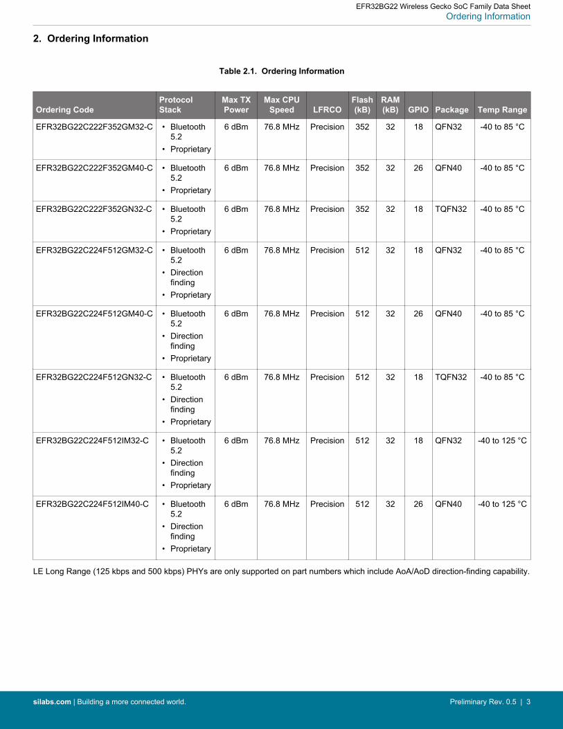
2. Ordering Information
Table 2.1. Ordering Information
Ordering CodeProtocolStack
Max TXPower
Max CPUSpeed LFRCO
Flash(kB)
RAM(kB) GPIO Package Temp Range
EFR32BG22C222F352GM32-C • Bluetooth5.2
• Proprietary
6 dBm 76.8 MHz Precision 352 32 18 QFN32 -40 to 85 °C
EFR32BG22C222F352GM40-C • Bluetooth5.2
• Proprietary
6 dBm 76.8 MHz Precision 352 32 26 QFN40 -40 to 85 °C
EFR32BG22C222F352GN32-C • Bluetooth5.2
• Proprietary
6 dBm 76.8 MHz Precision 352 32 18 TQFN32 -40 to 85 °C
EFR32BG22C224F512GM32-C • Bluetooth5.2
• Directionfinding
• Proprietary
6 dBm 76.8 MHz Precision 512 32 18 QFN32 -40 to 85 °C
EFR32BG22C224F512GM40-C • Bluetooth5.2
• Directionfinding
• Proprietary
6 dBm 76.8 MHz Precision 512 32 26 QFN40 -40 to 85 °C
EFR32BG22C224F512GN32-C • Bluetooth5.2
• Directionfinding
• Proprietary
6 dBm 76.8 MHz Precision 512 32 18 TQFN32 -40 to 85 °C
EFR32BG22C224F512IM32-C • Bluetooth5.2
• Directionfinding
• Proprietary
6 dBm 76.8 MHz Precision 512 32 18 QFN32 -40 to 125 °C
EFR32BG22C224F512IM40-C • Bluetooth5.2
• Directionfinding
• Proprietary
6 dBm 76.8 MHz Precision 512 32 26 QFN40 -40 to 125 °C
LE Long Range (125 kbps and 500 kbps) PHYs are only supported on part numbers which include AoA/AoD direction-finding capability.
EFR32BG22 Wireless Gecko SoC Family Data SheetOrdering Information
silabs.com | Building a more connected world. Preliminary Rev. 0.5 | 3
Table of Contents1. Feature List . . . . . . . . . . . . . . . . . . . . . . . . . . . . . . . . 2
2. Ordering Information . . . . . . . . . . . . . . . . . . . . . . . . . . . . 3
3. System Overview . . . . . . . . . . . . . . . . . . . . . . . . . . . . . . 73.1 Introduction . . . . . . . . . . . . . . . . . . . . . . . . . . . . . . . 7
3.2 Radio . . . . . . . . . . . . . . . . . . . . . . . . . . . . . . . . . 73.2.1 Antenna Interface . . . . . . . . . . . . . . . . . . . . . . . . . . . 73.2.2 Fractional-N Frequency Synthesizer . . . . . . . . . . . . . . . . . . . . . 83.2.3 Receiver Architecture . . . . . . . . . . . . . . . . . . . . . . . . . . 83.2.4 Transmitter Architecture . . . . . . . . . . . . . . . . . . . . . . . . . 83.2.5 Packet and State Trace . . . . . . . . . . . . . . . . . . . . . . . . . 83.2.6 Data Buffering. . . . . . . . . . . . . . . . . . . . . . . . . . . . . 83.2.7 Radio Controller (RAC). . . . . . . . . . . . . . . . . . . . . . . . . . 83.2.8 RFSENSE Interface . . . . . . . . . . . . . . . . . . . . . . . . . . . 9
3.3 General Purpose Input/Output (GPIO) . . . . . . . . . . . . . . . . . . . . . . 9
3.4 Clocking . . . . . . . . . . . . . . . . . . . . . . . . . . . . . . . . 93.4.1 Clock Management Unit (CMU) . . . . . . . . . . . . . . . . . . . . . . . 93.4.2 Internal and External Oscillators. . . . . . . . . . . . . . . . . . . . . . . 9
3.5 Counters/Timers and PWM . . . . . . . . . . . . . . . . . . . . . . . . . . 93.5.1 Timer/Counter (TIMER) . . . . . . . . . . . . . . . . . . . . . . . . . 93.5.2 Low Energy Timer (LETIMER) . . . . . . . . . . . . . . . . . . . . . . .103.5.3 Real Time Clock with Capture (RTCC) . . . . . . . . . . . . . . . . . . . .103.5.4 Back-Up Real Time Counter . . . . . . . . . . . . . . . . . . . . . . . .103.5.5 Watchdog Timer (WDOG) . . . . . . . . . . . . . . . . . . . . . . . . .10
3.6 Communications and Other Digital Peripherals . . . . . . . . . . . . . . . . . . .103.6.1 Universal Synchronous/Asynchronous Receiver/Transmitter (USART) . . . . . . . . . .103.6.2 Enhanced Universal Asynchronous Receiver/Transmitter (EUART) . . . . . . . . . . .103.6.3 Inter-Integrated Circuit Interface (I2C) . . . . . . . . . . . . . . . . . . . . .103.6.4 Peripheral Reflex System (PRS) . . . . . . . . . . . . . . . . . . . . . .113.6.5 Pulse Density Modulation (PDM) Interface . . . . . . . . . . . . . . . . . . .11
3.7 Security Features . . . . . . . . . . . . . . . . . . . . . . . . . . . . .113.7.1 Secure Boot with Root of Trust and Secure Loader (RTSL) . . . . . . . . . . . . .113.7.2 Cryptographic Accelerator. . . . . . . . . . . . . . . . . . . . . . . . .113.7.3 True Random Number Generator . . . . . . . . . . . . . . . . . . . . . .113.7.4 Secure Debug with Lock/Unlock. . . . . . . . . . . . . . . . . . . . . . .12
3.8 Analog. . . . . . . . . . . . . . . . . . . . . . . . . . . . . . . . .123.8.1 Analog to Digital Converter (IADC) . . . . . . . . . . . . . . . . . . . . . .12
3.9 Power . . . . . . . . . . . . . . . . . . . . . . . . . . . . . . . . .133.9.1 Energy Management Unit (EMU) . . . . . . . . . . . . . . . . . . . . . .133.9.2 Voltage Scaling . . . . . . . . . . . . . . . . . . . . . . . . . . . .133.9.3 DC-DC Converter . . . . . . . . . . . . . . . . . . . . . . . . . . .133.9.4 Power Domains . . . . . . . . . . . . . . . . . . . . . . . . . . . .13
3.10 Reset Management Unit (RMU) . . . . . . . . . . . . . . . . . . . . . . . .14
silabs.com | Building a more connected world. Preliminary Rev. 0.5 | 4
3.11 Core and Memory . . . . . . . . . . . . . . . . . . . . . . . . . . . .143.11.1 Processor Core . . . . . . . . . . . . . . . . . . . . . . . . . . . .143.11.2 Memory System Controller (MSC) . . . . . . . . . . . . . . . . . . . . .143.11.3 Linked Direct Memory Access Controller (LDMA) . . . . . . . . . . . . . . . .14
3.12 Memory Map . . . . . . . . . . . . . . . . . . . . . . . . . . . . . .15
3.13 Configuration Summary . . . . . . . . . . . . . . . . . . . . . . . . . .16
4. Electrical Specifications . . . . . . . . . . . . . . . . . . . . . . . . . . 174.1 Electrical Characteristics . . . . . . . . . . . . . . . . . . . . . . . . . .17
4.2 Absolute Maximum Ratings. . . . . . . . . . . . . . . . . . . . . . . . . .18
4.3 General Operating Conditions . . . . . . . . . . . . . . . . . . . . . . . . .19
4.4 DC-DC Converter . . . . . . . . . . . . . . . . . . . . . . . . . . . . .214.4.1 DC-DC Operating Limits . . . . . . . . . . . . . . . . . . . . . . . . .23
4.5 Thermal Characteristics . . . . . . . . . . . . . . . . . . . . . . . . . . .24
4.6 Current Consumption . . . . . . . . . . . . . . . . . . . . . . . . . . . .254.6.1 MCU current consumption using DC-DC at 3.0 V input . . . . . . . . . . . . . . .254.6.2 MCU current consumption at 3.0 V . . . . . . . . . . . . . . . . . . . . . .274.6.3 MCU current consumption at 1.8 V . . . . . . . . . . . . . . . . . . . . . .294.6.4 Radio current consumption at 3.0V using DCDC . . . . . . . . . . . . . . . . .31
4.7 Flash Characteristics . . . . . . . . . . . . . . . . . . . . . . . . . . . .33
4.8 Wake Up, Entry, and Exit times . . . . . . . . . . . . . . . . . . . . . . . .34
4.9 RFSENSE Low-energy Wake-on-RF . . . . . . . . . . . . . . . . . . . . . .35
4.10 2.4 GHz RF Transceiver Characteristics . . . . . . . . . . . . . . . . . . . . .364.10.1 RF Transmitter Characteristics . . . . . . . . . . . . . . . . . . . . . . .364.10.2 RF Receiver Characteristics . . . . . . . . . . . . . . . . . . . . . . .43
4.11 Oscillators . . . . . . . . . . . . . . . . . . . . . . . . . . . . . . .494.11.1 High Frequency Crystal Oscillator. . . . . . . . . . . . . . . . . . . . . .494.11.2 Low Frequency Crystal Oscillator . . . . . . . . . . . . . . . . . . . . . .504.11.3 High Frequency RC Oscillator (HFRCO) . . . . . . . . . . . . . . . . . . .514.11.4 Fast Start_Up RC Oscillator (FSRCO) . . . . . . . . . . . . . . . . . . . .524.11.5 Precision Low Frequency RC Oscillator (LFRCO) . . . . . . . . . . . . . . . .534.11.6 Ultra Low Frequency RC Oscillator . . . . . . . . . . . . . . . . . . . . .53
4.12 GPIO Pins (3V GPIO pins) . . . . . . . . . . . . . . . . . . . . . . . . .54
4.13 Analog to Digital Converter (IADC) . . . . . . . . . . . . . . . . . . . . . . .56
4.14 Temperature Sense . . . . . . . . . . . . . . . . . . . . . . . . . . . .58
4.15 Brown Out Detectors . . . . . . . . . . . . . . . . . . . . . . . . . . .594.15.1 DVDD BOD . . . . . . . . . . . . . . . . . . . . . . . . . . . . .594.15.2 LE DVDD BOD . . . . . . . . . . . . . . . . . . . . . . . . . . . .594.15.3 AVDD and IOVDD BODs . . . . . . . . . . . . . . . . . . . . . . . .60
4.16 PDM Timing Specifications . . . . . . . . . . . . . . . . . . . . . . . . .614.16.1 Pulse Density Modulator (PDM), Common DBUS . . . . . . . . . . . . . . . .61
4.17 USART SPI Master Timing . . . . . . . . . . . . . . . . . . . . . . . . .624.17.1 SPI Master Timing, Voltage Scaling = VSCALE2. . . . . . . . . . . . . . . . .63
silabs.com | Building a more connected world. Preliminary Rev. 0.5 | 5
4.17.2 SPI Master Timing, Voltage Scaling = VSCALE1. . . . . . . . . . . . . . . . .63
4.18 USART SPI Slave Timing . . . . . . . . . . . . . . . . . . . . . . . . . .644.18.1 SPI Slave Timing, Voltage Scaling = VSCALE2 . . . . . . . . . . . . . . . . .644.18.2 SPI Slave Timing, Voltage Scaling = VSCALE1 . . . . . . . . . . . . . . . . .65
4.19 I2C Electrical Specifications . . . . . . . . . . . . . . . . . . . . . . . . .664.19.1 I2C Standard-mode (Sm) . . . . . . . . . . . . . . . . . . . . . . . .664.19.2 I2C Fast-mode (Fm) . . . . . . . . . . . . . . . . . . . . . . . . . .674.19.3 I2C Fast-mode Plus (Fm+) . . . . . . . . . . . . . . . . . . . . . . . .68
4.20 Typical Performance Curves . . . . . . . . . . . . . . . . . . . . . . . . .684.20.1 Supply Current . . . . . . . . . . . . . . . . . . . . . . . . . . . .694.20.2 RF Characteristics . . . . . . . . . . . . . . . . . . . . . . . . . . .714.20.3 DC-DC Converter . . . . . . . . . . . . . . . . . . . . . . . . . . .72
5. Typical Connections . . . . . . . . . . . . . . . . . . . . . . . . . . .735.1 Power . . . . . . . . . . . . . . . . . . . . . . . . . . . . . . . . .73
5.2 RF Matching Networks . . . . . . . . . . . . . . . . . . . . . . . . . . .745.2.1 2.4 GHz Matching Network . . . . . . . . . . . . . . . . . . . . . . . .74
5.3 Other Connections. . . . . . . . . . . . . . . . . . . . . . . . . . . . .74
6. Pin Definitions . . . . . . . . . . . . . . . . . . . . . . . . . . . . . . 756.1 QFN32 Device Pinout . . . . . . . . . . . . . . . . . . . . . . . . . . .75
6.2 QFN40 Device Pinout . . . . . . . . . . . . . . . . . . . . . . . . . . .77
6.3 TQFN32 Device Pinout . . . . . . . . . . . . . . . . . . . . . . . . . . .79
6.4 Alternate Function Table. . . . . . . . . . . . . . . . . . . . . . . . . . .80
6.5 Analog Peripheral Connectivity . . . . . . . . . . . . . . . . . . . . . . . .81
6.6 Digital Peripheral Connectivity . . . . . . . . . . . . . . . . . . . . . . . . .82
7. QFN32 Package Specifications. . . . . . . . . . . . . . . . . . . . . . . . 857.1 QFN32 Package Dimensions . . . . . . . . . . . . . . . . . . . . . . . . .85
7.2 QFN32 PCB Land Pattern . . . . . . . . . . . . . . . . . . . . . . . . . .87
7.3 QFN32 Package Marking . . . . . . . . . . . . . . . . . . . . . . . . . .89
8. TQFN32 Package Specifications . . . . . . . . . . . . . . . . . . . . . . . 908.1 TQFN32 Package Dimensions. . . . . . . . . . . . . . . . . . . . . . . . .90
8.2 TQFN32 PCB Land Pattern. . . . . . . . . . . . . . . . . . . . . . . . . .92
8.3 TQFN32 Package Marking . . . . . . . . . . . . . . . . . . . . . . . . . .94
9. QFN40 Package Specifications. . . . . . . . . . . . . . . . . . . . . . . . 959.1 QFN40 Package Dimensions . . . . . . . . . . . . . . . . . . . . . . . . .95
9.2 QFN40 PCB Land Pattern . . . . . . . . . . . . . . . . . . . . . . . . . .97
9.3 QFN40 Package Marking . . . . . . . . . . . . . . . . . . . . . . . . . .98
10. Revision History. . . . . . . . . . . . . . . . . . . . . . . . . . . . . 99
silabs.com | Building a more connected world. Preliminary Rev. 0.5 | 6
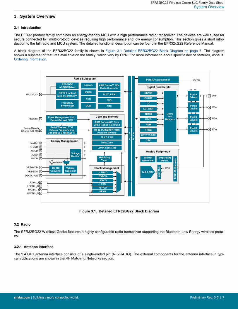
3. System Overview
3.1 Introduction
The EFR32 product family combines an energy-friendly MCU with a high performance radio transceiver. The devices are well suited forsecure connected IoT multi-protocol devices requiring high performance and low energy consumption. This section gives a short intro-duction to the full radio and MCU system. The detailed functional description can be found in the EFR32xG22 Reference Manual.
A block diagram of the EFR32BG22 family is shown in Figure 3.1 Detailed EFR32BG22 Block Diagram on page 7. The diagramshows a superset of features available on the family, which vary by OPN. For more information about specific device features, consult Ordering Information.
Analog Peripherals
Clock Management
HFRCO
Core and Memory
Up to 512 KB ISP FlashProgram Memory
32 KB RAMAHB
Watchdog Timer
RESETn
Digital Peripherals
Inpu
t Mux
DBUS Port
Mappers
Port I/O Configuration
12-bit ADCVDD
Internal Reference
IOVDD
LFXO
FSRCO
HFXO
Trust Zone
LFRCO
APB
LDMA Controller
AB
US
Mul
tiple
xers
CRC
I2C
USART
RTCC
TIMER
LETIMER
Port D Drivers PDn
Port C Drivers PCn
Port B Drivers PBn
Port ADrivers PAn
HFXTAL_IHFXTAL_O
LFXTAL_ILFXTAL_O
Debug Signals(shared w/GPIO)
Reset Management Unit, Brown Out and POR
Serial Wire and ETM Debug / Programming
with Debug Challenge I/F
RF2G4_IO
TRNG
ULFRCO
Temperature Sensor
EUART
PDM
Energy Management
DVDD
VREGVDD
VREGSW
bypass
AVDD
PAVDD
RFVDD
DECOUPLE
IOVDDVoltage Monitor
Voltage Regulator
DC-DC Converter
CRYPTOACC
ARM Cortex-M33 Core with Floating Point Unit
Radio Subsystem
RFSENSEw/ OOK Detect
RX/TX Frontend with Integrated PA
Frequency Synthesizer
ARM CortexTM M0+ Radio Controller
CRC
BUFC RAM
FRC
DEMOD
AGC
IFADC
MOD
Figure 3.1. Detailed EFR32BG22 Block Diagram
3.2 Radio
The EFR32BG22 Wireless Gecko features a highly configurable radio transceiver supporting the Bluetooth Low Energy wireless proto-col.
3.2.1 Antenna Interface
The 2.4 GHz antenna interface consists of a single-ended pin (RF2G4_IO). The external components for the antenna interface in typi-cal applications are shown in the RF Matching Networks section.
EFR32BG22 Wireless Gecko SoC Family Data SheetSystem Overview
silabs.com | Building a more connected world. Preliminary Rev. 0.5 | 7
3.2.2 Fractional-N Frequency Synthesizer
The EFR32BG22 contains a high performance, low phase noise, fully integrated fractional-N frequency synthesizer. The synthesizer isused in receive mode to generate the LO frequency for the down-conversion mixer. It is also used in transmit mode to directly generatethe modulated RF carrier.
The fractional-N architecture provides excellent phase noise performance, frequency resolution better than 100 Hz, and low energyconsumption. The synthesizer’s fast frequency settling allows for very short receiver and transmitter wake up times to reduce systemenergy consumption.
3.2.3 Receiver Architecture
The EFR32BG22 uses a low-IF receiver architecture, consisting of a Low-Noise Amplifier (LNA) followed by an I/Q down-conversionmixer. The I/Q signals are further filtered and amplified before being sampled by the IF analog-to-digital converter (IFADC).
The IF frequency is configurable from 150 kHz to 1371 kHz. The IF can further be configured for high-side or low-side injection, provid-ing flexibility with respect to known interferers at the image frequency.
The Automatic Gain Control (AGC) module adjusts the receiver gain to optimize performance and avoid saturation for excellent selec-tivity and blocking performance. The 2.4 GHz radio is calibrated at production to improve image rejection performance.
Demodulation is performed in the digital domain. The demodulator performs configurable decimation and channel filtering to allow re-ceive bandwidths ranging from 0.1 to 2530 kHz. High carrier frequency and baud rate offsets are tolerated by active estimation andcompensation. Advanced features supporting high quality communication under adverse conditions include forward error correction byblock and convolutional coding as well as Direct Sequence Spread Spectrum (DSSS).
A Received Signal Strength Indicator (RSSI) is available for signal quality metrics, for level-based proximity detection, and for RF chan-nel access by Collision Avoidance (CA) or Listen Before Talk (LBT) algorithms. An RSSI capture value is associated with each receivedframe and the dynamic RSSI measurement can be monitored throughout reception.
3.2.4 Transmitter Architecture
The EFR32BG22 uses a direct-conversion transmitter architecture. For constant envelope modulation formats, the modulator controlsphase and frequency modulation in the frequency synthesizer. Transmit symbols or chips are optionally shaped by a digital shapingfilter. The shaping filter is fully configurable, including the BT product, and can be used to implement Gaussian or Raised Cosine shap-ing.
Carrier Sense Multiple Access - Collision Avoidance (CSMA-CA) or Listen Before Talk (LBT) algorithms can be automatically timed bythe EFR32BG22. These algorithms are typically defined by regulatory standards to improve inter-operability in a given bandwidth be-tween devices that otherwise lack synchronized RF channel access.
3.2.5 Packet and State Trace
The EFR32BG22 Frame Controller has a packet and state trace unit that provides valuable information during the development phase.It features:• Non-intrusive trace of transmit data, receive data and state information• Data observability on a single-pin UART data output, or on a two-pin SPI data output• Configurable data output bitrate / baudrate• Multiplexed transmitted data, received data and state / meta information in a single serial data stream
3.2.6 Data Buffering
The EFR32BG22 features an advanced Radio Buffer Controller (BUFC) capable of handling up to 4 buffers of adjustable size from 64bytes to 4096 bytes. Each buffer can be used for RX, TX or both. The buffer data is located in RAM, enabling zero-copy operations.
3.2.7 Radio Controller (RAC)
The Radio Controller controls the top level state of the radio subsystem in the EFR32BG22. It performs the following tasks:• Precisely-timed control of enabling and disabling of the receiver and transmitter circuitry• Run-time calibration of receiver, transmitter and frequency synthesizer• Detailed frame transmission timing, including optional LBT or CSMA-CA
EFR32BG22 Wireless Gecko SoC Family Data SheetSystem Overview
silabs.com | Building a more connected world. Preliminary Rev. 0.5 | 8
3.2.8 RFSENSE Interface
The RFSENSE block allows the device to remain in EM2, EM3 or EM4 and wake when RF energy above a specified threshold is detec-ted. When operated in selective mode, the RFSENSE block performs OOK preamble and sync word detection, preventing false wake-up events.
3.3 General Purpose Input/Output (GPIO)
EFR32BG22 has up to 26 General Purpose Input/Output pins. Each GPIO pin can be individually configured as either an output orinput. More advanced configurations including open-drain, open-source, and glitch-filtering can be configured for each individual GPIOpin. The GPIO pins can be overridden by peripheral connections, like SPI communication. Each peripheral connection can be routed toseveral GPIO pins on the device. The input value of a GPIO pin can be routed through the Peripheral Reflex System to other peripher-als. The GPIO subsystem supports asynchronous external pin interrupts.
All of the pins on ports A and port B are EM2 capable. These pins may be used by Low-Energy peripherals in EM2/3 and may also beused as EM2/3 pin wake-ups. Pins on ports C and D are latched/retained in their current state when entering EM2 until EM2 exit uponwhich internal peripherals could once again drive those pads.
A few GPIOs also have EM4 wake functionality. These pins are listed in the Alternate Function Table.
3.4 Clocking
3.4.1 Clock Management Unit (CMU)
The Clock Management Unit controls oscillators and clocks in the EFR32BG22. Individual enabling and disabling of clocks to all periph-eral modules is performed by the CMU. The CMU also controls enabling and configuration of the oscillators. A high degree of flexibilityallows software to optimize energy consumption in any specific application by minimizing power dissipation in unused peripherals andoscillators.
3.4.2 Internal and External Oscillators
The EFR32BG22 supports two crystal oscillators and fully integrates four RC oscillators, listed below.• A high frequency crystal oscillator (HFXO) with integrated load capacitors, tunable in small steps, provides a precise timing refer-
ence for the MCU. The HFXO provides excellent RF clocking performance using a 38.4 MHz crystal. The HFXO can also support anexternal clock source such as a TCXO for applications that require an extremely accurate clock frequency over temperature.
• A 32.768 kHz crystal oscillator (LFXO) provides an accurate timing reference for low energy modes.• An integrated high frequency RC oscillator (HFRCO) is available for the MCU system, when crystal accuracy is not required. The
HFRCO employs fast start-up at minimal energy consumption combined with a wide frequency range, from 1 MHz to 76.8 MHz.• An integrated fast start-up RC oscillator (FSRCO) that runs at a fixed 20 MHz• An integrated low frequency 32.768 kHz RC oscillator (LFRCO) for low power operation without an external crystal. Precision mode
enables periodic recalibration against the 38.4 MHz HFXO crystal to improve accuracy to +/- 500 ppm, suitable for BLE sleep inter-val timing.
• An integrated ultra-low frequency 1 kHz RC oscillator (ULFRCO) is available to provide a timing reference at the lowest energy con-sumption in low energy modes.
3.5 Counters/Timers and PWM
3.5.1 Timer/Counter (TIMER)
TIMER peripherals keep track of timing, count events, generate PWM outputs and trigger timed actions in other peripherals through thePeripheral Reflex System (PRS). The core of each TIMER is a 16-bit or 32-bit counter with up to 3 compare/capture channels. Eachchannel is configurable in one of three modes. In capture mode, the counter state is stored in a buffer at a selected input event. Incompare mode, the channel output reflects the comparison of the counter to a programmed threshold value. In PWM mode, the TIMERsupports generation of pulse-width modulation (PWM) outputs of arbitrary waveforms defined by the sequence of values written to thecompare registers. In addition some timers offer dead-time insertion.
See 3.13 Configuration Summary for information on the feature set of each timer.
EFR32BG22 Wireless Gecko SoC Family Data SheetSystem Overview
silabs.com | Building a more connected world. Preliminary Rev. 0.5 | 9
3.5.2 Low Energy Timer (LETIMER)
The unique LETIMER is a 24-bit timer that is available in energy mode EM0 Active, EM1 Sleep, EM2 Deep Sleep, and EM3 Stop. Thisallows it to be used for timing and output generation when most of the device is powered down, allowing simple tasks to be performedwhile the power consumption of the system is kept at an absolute minimum. The LETIMER can be used to output a variety of wave-forms with minimal software intervention. The LETIMER is connected to the Peripheral Reflex System (PRS), and can be configured tostart counting on compare matches from other peripherals such as the RTCC.
3.5.3 Real Time Clock with Capture (RTCC)
The Real Time Clock with Capture (RTCC) is a 32-bit counter providing timekeeping down to EM3. The RTCC can be clocked by any ofthe on-board low-frequency oscillators, and it is capable of providing system wake-up at user defined intervals.
A secondary RTC is used by the RF protocol stack for event scheduling, leaving the primary RTCC block available exclusively for appli-cation software.
3.5.4 Back-Up Real Time Counter
The Back-Up Real Time Counter (BURTC) is a 32-bit counter providing timekeeping in all energy modes, including EM4. The BURTCcan be clocked by any of the on-board low-frequency oscillators, and it is capable of providing system wake-up at user defined inver-vals.
3.5.5 Watchdog Timer (WDOG)
The watchdog timer can act both as an independent watchdog or as a watchdog synchronous with the CPU clock. It has windowedmonitoring capabilities, and can generate a reset or different interrupts depending on the failure mode of the system. The watchdog canalso monitor autonomous systems driven by the Peripheral Reflex System (PRS).
3.6 Communications and Other Digital Peripherals
3.6.1 Universal Synchronous/Asynchronous Receiver/Transmitter (USART)
The Universal Synchronous/Asynchronous Receiver/Transmitter is a flexible serial I/O module. It supports full duplex asynchronousUART communication with hardware flow control as well as RS-485, SPI, MicroWire and 3-wire. It can also interface with devices sup-porting:• ISO7816 SmartCards• IrDA• I2S
3.6.2 Enhanced Universal Asynchronous Receiver/Transmitter (EUART)
The Enhanced Universal Asynchronous Receiver/Transmitter supports full duplex asynchronous UART communication with hardwareflow control, RS-485 and IrDA support. In EM0 and EM1 the EUART provides a high-speed, buffered communication interface.
When routed to GPIO ports A or B, the EUART may also be used in a low-energy mode and operate in EM2. A 32.768 kHz clocksource allows full duplex UART communication up to 9600 baud.
3.6.3 Inter-Integrated Circuit Interface (I2C)
The I2C module provides an interface between the MCU and a serial I2C bus. It is capable of acting as both a master and a slave andsupports multi-master buses. Standard-mode, fast-mode and fast-mode plus speeds are supported, allowing transmission rates from 10kbit/s up to 1 Mbit/s. Slave arbitration and timeouts are also available, allowing implementation of an SMBus-compliant system. Theinterface provided to software by the I2C module allows precise timing control of the transmission process and highly automated trans-fers. Automatic recognition of slave addresses is provided in active and low energy modes. Note that not all instances of I2C are avalia-ble in all energy modes.
EFR32BG22 Wireless Gecko SoC Family Data SheetSystem Overview
silabs.com | Building a more connected world. Preliminary Rev. 0.5 | 10
3.6.4 Peripheral Reflex System (PRS)
The Peripheral Reflex System provides a communication network between different peripheral modules without software involvement.Peripheral modules producing Reflex signals are called producers. The PRS routes Reflex signals from producers to consumer periph-erals which in turn perform actions in response. Edge triggers and other functionality such as simple logic operations (AND, OR, NOT)can be applied by the PRS to the signals. The PRS allows peripherals to act autonomously without waking the MCU core, savingpower.
3.6.5 Pulse Density Modulation (PDM) Interface
The PDM module provides a serial interface and decimation filter for Pulse Density Modulation (PDM) microphones, isolated Sigma-delta ADCs, digital sensors and other PDM or sigma delta bit stream peripherals. A programmable Cascaded Integrator Comb (CIC)filter is used to decimate the incoming bit streams. PDM supports stereo or mono input data and DMA transfer.
3.7 Security Features
The following security features are available on the EFR32BG22:• Secure Boot with Root of Trust and Secure Loader (RTSL)• Cryptographic Accelerator• True Random Number Generator (TRNG)• Secure Debug with Lock/Unlock
3.7.1 Secure Boot with Root of Trust and Secure Loader (RTSL)
The Secure Boot with RTSL authenticates a chain of trusted firmware that begins from an immutable memory (ROM).
It prevents malware injection, prevents rollback, ensures that only authentic firmware is executed and protects Over The Air updates.
More information on this feature can be found in the Application Note AN1218: Series 2 Secure Boot with RTSL.
3.7.2 Cryptographic Accelerator
The Cryptographic Accelerator is an autonomous hardware accelerator with Differential Power Analysis (DPA) countermeasures to pro-tect keys.
It supports AES encryption and decryption with 128/192/256-bit keys, Elliptic Curve Cryptography(ECC) to support public key opera-tions and hashes.
Supported block cipher modes of operation for AES include:• ECB (Electronic Code Book)• CTR (Counter Mode)• CBC (Cipher Block Chaining)• CFB (Cipher Feedback)• GCM (Galois Counter Mode)• CBC-MAC (Cipher Block Chaining Message Authentication Code)• GMAC (Galois Message Authentication Code)• CCM (Counter with CBC-MAC)
The Cryptographic Accelerator accelerates Elliptical Curve Cryptography and supports the NIST (National Institute of Standards andTechnology) recommended curves including P-192 and P-256 for ECDH(Elliptic Curve Diffie-Hellman) key derivation and ECDSA (El-liptic Curve Digital Signature Algorithm) sign and verify operations.
Supported hashes include SHA-1, SHA2/224, and SHA-2/256.
This implementation provides a fast and energy efficient solution to state of the art cryptographic needs.
3.7.3 True Random Number Generator
The True Random Number Generator module is a non-deterministic random number generator that harvests entropy from a thermalenergy source. It includes start-up health tests for the entropy source as required by NIST SP800-90B and AIS-31 as well as onlinehealth tests required for NIST SP800-90C.
The TRNG is suitable for periodically generating entropy to seed an approved pseudo random number generator.
EFR32BG22 Wireless Gecko SoC Family Data SheetSystem Overview
silabs.com | Building a more connected world. Preliminary Rev. 0.5 | 11
3.7.4 Secure Debug with Lock/Unlock
For obvious security reasons, it is critical for a product to have its debug interface locked before being released in the field.
In addition, the Secure Element also provides a secure debug unlock function that allows authenticated access based on public keycryptography. This functionality is particularly useful for supporting failure analysis while maintaining confidentiality of IP and sensitiveend-user data.
More information on this feature can be found in the Application Note AN1190: EFR32xG2x Secure Debug.
3.8 Analog
3.8.1 Analog to Digital Converter (IADC)
The IADC is a hybrid architecture combining techniques from both SAR and Delta-Sigma style converters. It has a resolution of up to 12bits at up to 1 Msps. Hardware oversampling reduces system-level noise over multiple front-end samples. The IADC includes integratedvoltage references. Inputs are selectable from a wide range of sources, including pins configurable as either single-ended or differential.
EFR32BG22 Wireless Gecko SoC Family Data SheetSystem Overview
silabs.com | Building a more connected world. Preliminary Rev. 0.5 | 12
3.9 Power
The EFR32BG22 has an Energy Management Unit (EMU) and efficient integrated regulators to generate internal supply voltages. Onlya single external supply voltage is required, from which all internal voltages are created. An optional integrated DC-DC buck regulatorcan be utilized to further reduce the current consumption. The DC-DC regulator requires one external inductor and one external capaci-tor.
The EFR32BG22 device family includes support for internal supply voltage scaling, as well as two different power domains groups forperipherals. These enhancements allow for further supply current reductions and lower overall power consumption.
3.9.1 Energy Management Unit (EMU)
The Energy Management Unit manages transitions of energy modes in the device. Each energy mode defines which peripherals andfeatures are available and the amount of current the device consumes. The EMU can also be used to implement system-wide voltagescaling and turn off the power to unused RAM blocks to optimize the energy consumption in the target application. The DC-DC regula-tor operation is tightly integrated with the EMU.
3.9.2 Voltage Scaling
The EFR32BG22 supports supply voltage scaling for the LDO powering DECOUPLE, with independent selections for EM0 / EM1 andEM2 / EM3. Voltage scaling helps to optimize the energy efficiency of the system by operating at lower voltages when possible. Thedefault EM0 / EM1 voltage scaling level is VSCALE2, which allows the core to operate in active mode at full speed. The intermediatelevel, VSCALE1, allows operation in EM0 and EM1 at up to 40 MHz. The lowest level, VSCALE0, can be used to conserve power inEM2 and EM3. The EMU will automatically switch the target voltage scaling level when transitioning between energy modes.
3.9.3 DC-DC Converter
The DC-DC buck converter covers a wide range of load currents, provides high efficiency in energy modes EM0, EM1, EM2 and EM3,and can supply up to 60 mA for device and radio operation. RF noise mitigation allows operation of the DC-DC converter without signifi-cantly degrading sensitivity of radio components. An on-chip supply-monitor signals when the supply voltage is low to allow bypass ofthe regulator via programmable software interrupt. It employs soft switching at boot and DCDC regulating-to-bypass transitions to limitthe max supply slew-rate and mitigate inrush current.
3.9.4 Power Domains
The EFR32BG22 has three peripheral power domains for operation in EM2 and EM3, as well as the ability to selectively retain configu-rations for EM0/EM1 peripherals. A small set of peripherals always remain powered on in EM2 and EM3, including all peripherals whichare available in EM4. If all of the peripherals in PD0B or PD0C are configured as unused, that power domain will be powered off in EM2or EM3, reducing the overall current consumption of the device. Likewise, if the application can tolerate the setup time to re-configureused EM0/EM1 peripherals on wake, register retention for these peripherals can be disabled to further reduce the EM2 or EM3 current.
Table 3.1. Peripheral Power Subdomains
Always available in EM2/EM3 Power Domain PD0B Power Domain PD0C
RTCC LETIMER0 LFRCO (Precision Mode)
LFRCO (Non-precision mode)1 IADC0
LFXO1 I2C0
BURTC1 WDOG0
RFSENSE1 EUART0
ULFRCO1 PRS
FSRCO DEBUG
Note:1. Peripheral also available in EM4.
EFR32BG22 Wireless Gecko SoC Family Data SheetSystem Overview
silabs.com | Building a more connected world. Preliminary Rev. 0.5 | 13
3.10 Reset Management Unit (RMU)
The RMU is responsible for handling reset of the EFR32BG22. A wide range of reset sources are available, including several powersupply monitors, pin reset, software controlled reset, core lockup reset, and watchdog reset.
3.11 Core and Memory
3.11.1 Processor Core
The ARM Cortex-M processor includes a 32-bit RISC processor integrating the following features and tasks in the system:• ARM Cortex-M33 RISC processor achieving 1.50 Dhrystone MIPS/MHz• ARM TrustZone security technology• Embedded Trace Macrocell (ETM) for real-time trace and debug• Up to 512 kB flash program memory• Up to 32 kB RAM data memory• Configuration and event handling of all modules• 2-pin Serial-Wire debug interface
3.11.2 Memory System Controller (MSC)
The Memory System Controller (MSC) is the program memory unit of the microcontroller. The flash memory is readable and writablefrom both the Cortex-M and DMA. In addition to the main flash array where Program code is normally written the MSC also provides anInformation block where additional information such as special user information or flash-lock bits are stored. There is also a read-onlypage in the information block containing system and device calibration data. Read and write operations are supported in energy modesEM0 Active and EM1 Sleep.
3.11.3 Linked Direct Memory Access Controller (LDMA)
The Linked Direct Memory Access (LDMA) controller allows the system to perform memory operations independently of software. Thisreduces both energy consumption and software workload. The LDMA allows operations to be linked together and staged, enabling so-phisticated operations to be implemented.
EFR32BG22 Wireless Gecko SoC Family Data SheetSystem Overview
silabs.com | Building a more connected world. Preliminary Rev. 0.5 | 14
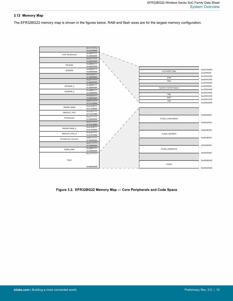
3.12 Memory Map
The EFR32BG22 memory map is shown in the figures below. RAM and flash sizes are for the largest memory configuration.
Figure 3.2. EFR32BG22 Memory Map — Core Peripherals and Code Space
EFR32BG22 Wireless Gecko SoC Family Data SheetSystem Overview
silabs.com | Building a more connected world. Preliminary Rev. 0.5 | 15
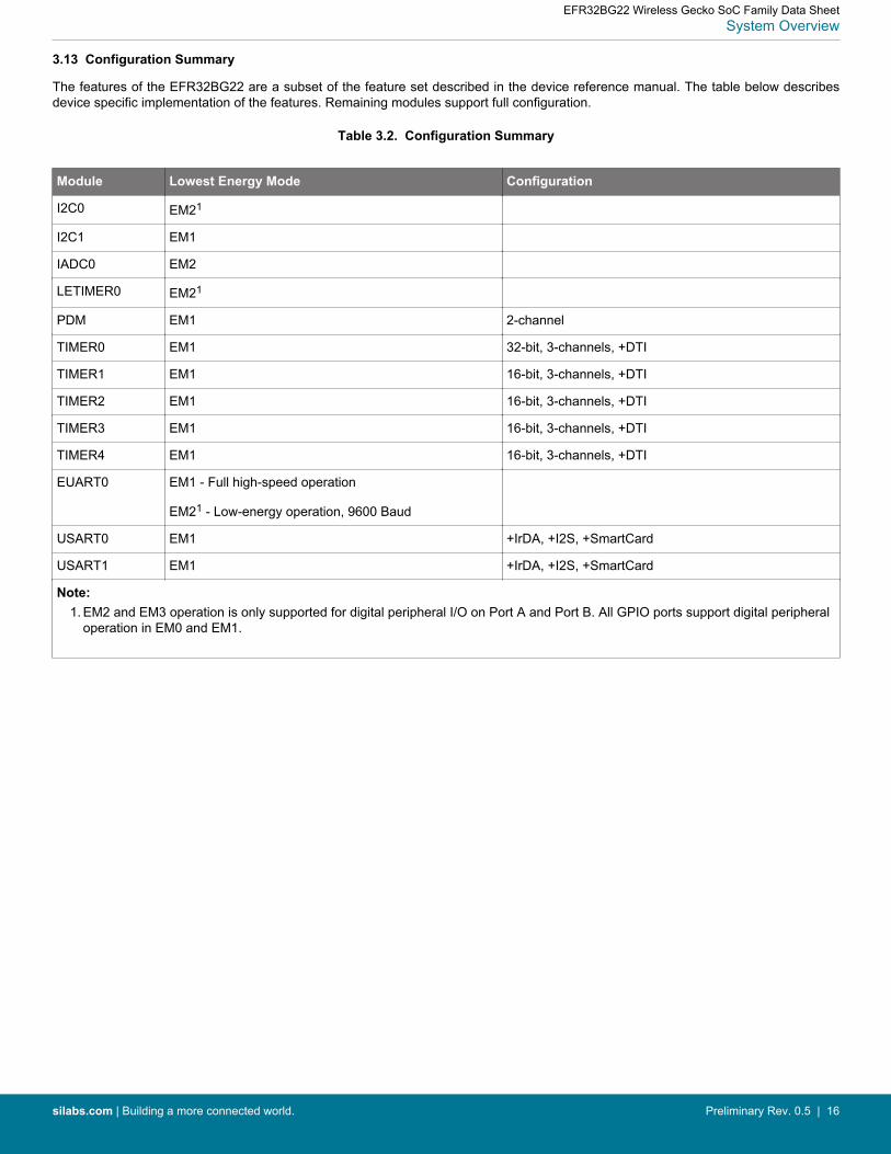
3.13 Configuration Summary
The features of the EFR32BG22 are a subset of the feature set described in the device reference manual. The table below describesdevice specific implementation of the features. Remaining modules support full configuration.
Table 3.2. Configuration Summary
Module Lowest Energy Mode Configuration
I2C0 EM21
I2C1 EM1
IADC0 EM2
LETIMER0 EM21
PDM EM1 2-channel
TIMER0 EM1 32-bit, 3-channels, +DTI
TIMER1 EM1 16-bit, 3-channels, +DTI
TIMER2 EM1 16-bit, 3-channels, +DTI
TIMER3 EM1 16-bit, 3-channels, +DTI
TIMER4 EM1 16-bit, 3-channels, +DTI
EUART0 EM1 - Full high-speed operation
EM21 - Low-energy operation, 9600 Baud
USART0 EM1 +IrDA, +I2S, +SmartCard
USART1 EM1 +IrDA, +I2S, +SmartCard
Note:1. EM2 and EM3 operation is only supported for digital peripheral I/O on Port A and Port B. All GPIO ports support digital peripheral
operation in EM0 and EM1.
EFR32BG22 Wireless Gecko SoC Family Data SheetSystem Overview
silabs.com | Building a more connected world. Preliminary Rev. 0.5 | 16
4. Electrical Specifications
4.1 Electrical Characteristics
All electrical parameters in all tables are specified under the following conditions, unless stated otherwise:• Typical values are based on TA=25 °C and all supplies at 3.0 V, by production test and/or technology characterization.• Radio performance numbers are measured in conducted mode, based on Silicon Laboratories reference designs using output pow-
er-specific external RF impedance-matching networks for interfacing to a 50 Ω antenna.• Minimum and maximum values represent the worst conditions across supply voltage, process variation, and operating temperature,
unless stated otherwise.
When assigning supply sources, the following requirements must be observed:• VREGVDD ≥ DVDD
• In systems not using the DCDC converter, DVDD should be shorted to VREGVDD• PAVDD ≥ RFVDD• AVDD and IOVDD: No dependency with each other or any other supply pin
EFR32BG22 Wireless Gecko SoC Family Data SheetElectrical Specifications
silabs.com | Building a more connected world. Preliminary Rev. 0.5 | 17
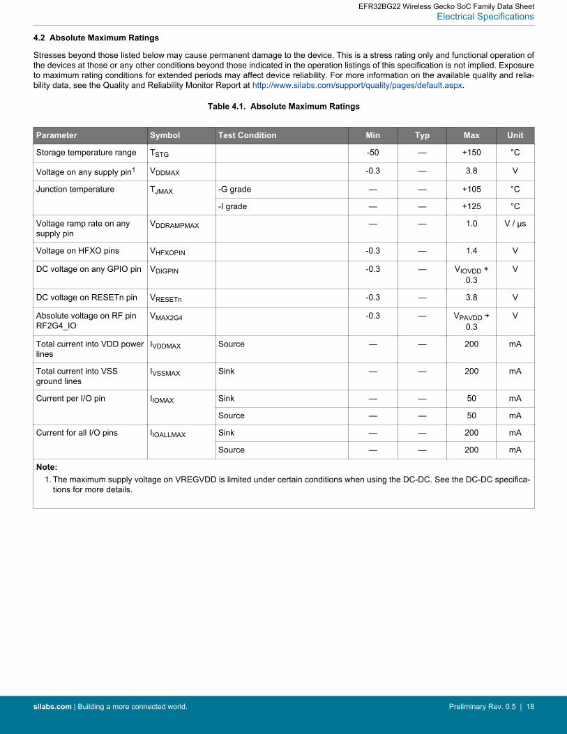
4.2 Absolute Maximum Ratings
Stresses beyond those listed below may cause permanent damage to the device. This is a stress rating only and functional operation ofthe devices at those or any other conditions beyond those indicated in the operation listings of this specification is not implied. Exposureto maximum rating conditions for extended periods may affect device reliability. For more information on the available quality and relia-bility data, see the Quality and Reliability Monitor Report at http://www.silabs.com/support/quality/pages/default.aspx.
Table 4.1. Absolute Maximum Ratings
Parameter Symbol Test Condition Min Typ Max Unit
Storage temperature range TSTG -50 — +150 °C
Voltage on any supply pin1 VDDMAX -0.3 — 3.8 V
Junction temperature TJMAX -G grade — — +105 °C
-I grade — — +125 °C
Voltage ramp rate on anysupply pin
VDDRAMPMAX — — 1.0 V / µs
Voltage on HFXO pins VHFXOPIN -0.3 — 1.4 V
DC voltage on any GPIO pin VDIGPIN -0.3 — VIOVDD +0.3
V
DC voltage on RESETn pin VRESETn -0.3 — 3.8 V
Absolute voltage on RF pinRF2G4_IO
VMAX2G4 -0.3 — VPAVDD +0.3
V
Total current into VDD powerlines
IVDDMAX Source — — 200 mA
Total current into VSSground lines
IVSSMAX Sink — — 200 mA
Current per I/O pin IIOMAX Sink — — 50 mA
Source — — 50 mA
Current for all I/O pins IIOALLMAX Sink — — 200 mA
Source — — 200 mA
Note:1. The maximum supply voltage on VREGVDD is limited under certain conditions when using the DC-DC. See the DC-DC specifica-
tions for more details.
EFR32BG22 Wireless Gecko SoC Family Data SheetElectrical Specifications
silabs.com | Building a more connected world. Preliminary Rev. 0.5 | 18
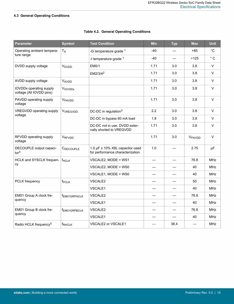
4.3 General Operating Conditions
Table 4.2. General Operating Conditions
Parameter Symbol Test Condition Min Typ Max Unit
Operating ambient tempera-ture range
TA -G temperature grade 1 -40 — +85 °C
-I temperature grade 1 -40 — +125 ° C
DVDD supply voltage VDVDD EM0/1 1.71 3.0 3.8 V
EM2/3/42 1.71 3.0 3.8 V
AVDD supply voltage VAVDD 1.71 3.0 3.8 V
IOVDDx operating supplyvoltage (All IOVDD pins)
VIOVDDx 1.71 3.0 3.8 V
PAVDD operating supplyvoltage
VPAVDD 1.71 3.0 3.8 V
VREGVDD operating supplyvoltage
VVREGVDD DC-DC in regulation3 2.2 3.0 3.8 V
DC-DC in bypass 60 mA load 1.8 3.0 3.8 V
DC-DC not in use. DVDD exter-nally shorted to VREGVDD
1.71 3.0 3.8 V
RFVDD operating supplyvoltage
VRFVDD 1.71 3.0 VPAVDD V
DECOUPLE output capaci-tor4
CDECOUPLE 1.0 µF ± 10% X8L capacitor usedfor performance characterization.
1.0 — 2.75 µF
HCLK and SYSCLK frequen-cy
fHCLK VSCALE2, MODE = WS1 — — 76.8 MHz
VSCALE2, MODE = WS0 — — 40 MHz
VSCALE1, MODE = WS0 — — 40 MHz
PCLK frequency fPCLK VSCALE2 — — 50 MHz
VSCALE1 — — 40 MHz
EM01 Group A clock fre-quency
fEM01GRPACLK VSCALE2 — — 76.8 MHz
VSCALE1 — — 40 MHz
EM01 Group B clock fre-quency
fEM01GRPBCLK VSCALE2 — — 76.8 MHz
VSCALE1 — — 40 MHz
Radio HCLK frequency5 fRHCLK VSCALE2 or VSCALE1 — 38.4 — MHz
EFR32BG22 Wireless Gecko SoC Family Data SheetElectrical Specifications
silabs.com | Building a more connected world. Preliminary Rev. 0.5 | 19
Parameter Symbol Test Condition Min Typ Max Unit
Note:1. The device may operate continuously at the maximum allowable ambient TA rating as long as the absolute maximum TJMAX is not
exceeded. For an application with significant power dissipation, the allowable TA may be lower than the maximum TA rating. TA =TJMAX - (THETAJA x PowerDissipation). Refer to the Absolute Maximum Ratings table and the Thermal Characteristics table forTJMAX and THETAJA.
2. The DVDD supply is monitored by the DVDD BOD in EM0/1 and the LE DVDD BOD in EM2/3/4.3. The maximum supply voltage on VREGVDD is limited under certain conditions when using the DC-DC. See the DC-DC specifica-
tions for more details.4. Murata GCM21BL81C105KA58L used for performance charaacterization. Actual capacitor values can be significantly de-rated
from their specified nominal value by the rated tolerance, as well as the application's AC voltage, DC bias, and temperature. Theminimum capacitance counting all error sources should be no less than 0.6 µF.
5. The recommended radio crystal frequency is 38.4 MHz. Any crystal frequency other than 38.4 is expressly not supported. SeeHFXO specifications for more detail on crystal tolerance.
EFR32BG22 Wireless Gecko SoC Family Data SheetElectrical Specifications
silabs.com | Building a more connected world. Preliminary Rev. 0.5 | 20
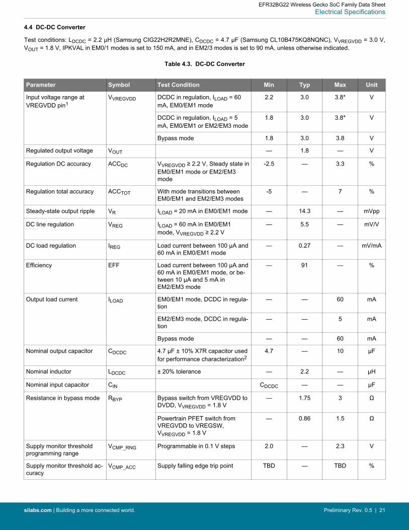
4.4 DC-DC Converter
Test conditions: LDCDC = 2.2 µH (Samsung CIG22H2R2MNE), CDCDC = 4.7 µF (Samsung CL10B475KQ8NQNC), VVREGVDD = 3.0 V,VOUT = 1.8 V, IPKVAL in EM0/1 modes is set to 150 mA, and in EM2/3 modes is set to 90 mA, unless otherwise indicated.
Table 4.3. DC-DC Converter
Parameter Symbol Test Condition Min Typ Max Unit
Input voltage range atVREGVDD pin1
VVREGVDD DCDC in regulation, ILOAD = 60mA, EM0/EM1 mode
2.2 3.0 3.8* V
DCDC in regulation, ILOAD = 5mA, EM0/EM1 or EM2/EM3 mode
1.8 3.0 3.8* V
Bypass mode 1.8 3.0 3.8 V
Regulated output voltage VOUT — 1.8 — V
Regulation DC accuracy ACCDC VVREGVDD ≥ 2.2 V, Steady state inEM0/EM1 mode or EM2/EM3mode
-2.5 — 3.3 %
Regulation total accuracy ACCTOT With mode transitions betweenEM0/EM1 and EM2/EM3 modes
-5 — 7 %
Steady-state output ripple VR ILOAD = 20 mA in EM0/EM1 mode — 14.3 — mVpp
DC line regulation VREG ILOAD = 60 mA in EM0/EM1mode, VVREGVDD ≥ 2.2 V
— 5.5 — mV/V
DC load regulation IREG Load current between 100 µA and60 mA in EM0/EM1 mode
— 0.27 — mV/mA
Efficiency EFF Load current between 100 µA and60 mA in EM0/EM1 mode, or be-tween 10 µA and 5 mA inEM2/EM3 mode
— 91 — %
Output load current ILOAD EM0/EM1 mode, DCDC in regula-tion
— — 60 mA
EM2/EM3 mode, DCDC in regula-tion
— — 5 mA
Bypass mode — — 60 mA
Nominal output capacitor CDCDC 4.7 µF ± 10% X7R capacitor usedfor performance characterization2
4.7 — 10 µF
Nominal inductor LDCDC ± 20% tolerance — 2.2 — µH
Nominal input capacitor CIN CDCDC — — µF
Resistance in bypass mode RBYP Bypass switch from VREGVDD toDVDD, VVREGVDD = 1.8 V
— 1.75 3 Ω
Powertrain PFET switch fromVREGVDD to VREGSW,VVREGVDD = 1.8 V
— 0.86 1.5 Ω
Supply monitor thresholdprogramming range
VCMP_RNG Programmable in 0.1 V steps 2.0 — 2.3 V
Supply monitor threshold ac-curacy
VCMP_ACC Supply falling edge trip point TBD — TBD %
EFR32BG22 Wireless Gecko SoC Family Data SheetElectrical Specifications
silabs.com | Building a more connected world. Preliminary Rev. 0.5 | 21
Parameter Symbol Test Condition Min Typ Max Unit
Supply monitor thresholdhysteresis
VCMP_HYST Positive hysteresis on the supplyrising edge referred to the fallingedge trip point
— 4 — %
Supply monitor responsetime
tCMP_DELAY Supply falling edge at -100 mV /µs
— 0.6 — µs
Note:1. The supported maximum VVREGVDD in regulation mode is a function of temperature and 10-year lifetime average load current.
See more details in 4.4.1 DC-DC Operating Limits.2. Samsung CL10B475KQ8NQNC used for performance charaacterization. Actual capacitor values can be significantly de-rated
from their specified nominal value by the rated tolerance, as well as the application's AC voltage, DC bias, and temperature. Theminimum capacitance counting all error sources should be no less than 2.4 µF.
EFR32BG22 Wireless Gecko SoC Family Data SheetElectrical Specifications
silabs.com | Building a more connected world. Preliminary Rev. 0.5 | 22
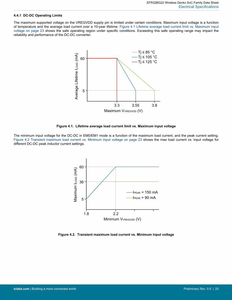
4.4.1 DC-DC Operating Limits
The maximum supported voltage on the VREGVDD supply pin is limited under certain conditions. Maximum input voltage is a functionof temperature and the average load current over a 10-year lifetime. Figure 4.1 Lifetime average load current limit vs. Maximum inputvoltage on page 23 shows the safe operating region under specific conditions. Exceeding this safe operating range may impact thereliability and performance of the DC-DC converter.
Aver
age
Life
time
I LOA
D (m
A)
Maximum VVREGVDD (V)
60
5
3.3 3.55 3.8
Tj ≤ 85 °CTj ≤ 105 °CTj ≤ 125 °C
Figure 4.1. Lifetime average load current limit vs. Maximum input voltage
The minimum input voltage for the DC-DC in EM0/EM1 mode is a function of the maximum load current, and the peak current setting.Figure 4.2 Transient maximum load current vs. Minimum input voltage on page 23 shows the max load current vs. input voltage fordifferent DC-DC peak inductor current settings.
Max
imum
I LO
AD (m
A)
Minimum VVREGVDD (V)
60
5
2.21.8
36
IPEAK = 150 mAIPEAK = 90 mA
Figure 4.2. Transient maximum load current vs. Minimum input voltage
EFR32BG22 Wireless Gecko SoC Family Data SheetElectrical Specifications
silabs.com | Building a more connected world. Preliminary Rev. 0.5 | 23
4.5 Thermal Characteristics
Table 4.4. Thermal Characteristics
Parameter Symbol Test Condition Min Typ Max Unit
Thermal Resistance Junctionto Ambient QFN32 (4x4mm)Package
THE-TAJA_QFN32_4X4
4-Layer PCB, Natural Convection1 — 35.4 — °C/W
Thermal Resistance Junctionto Ambient TQFN32(4x4mm) Package
THE-TAJA_TQFN32_4X
4
4-Layer PCB, Natural Convection1 — 40.2 — °C/W
Thermal Resistance, Junc-tion to Ambient, QFN40(5x5mm) Package
THE-TAJA_QFN40_5X5
4-Layer PCB, Natural Convection1 — 32.6 — °C/W
Note:1. Measured according to JEDEC standard JESD51-2A. Integrated Circuit Thermal Test Method Environmental Conditions - Natural
Convection (Still Air).
EFR32BG22 Wireless Gecko SoC Family Data SheetElectrical Specifications
silabs.com | Building a more connected world. Preliminary Rev. 0.5 | 24
4.6 Current Consumption
4.6.1 MCU current consumption using DC-DC at 3.0 V input
Unless otherwise indicated, typical conditions are: VREGVDD = 3.0 V. AVDD = DVDD = IOVDD = RFVDD = PAVDD = 1.8 V from DC-DC. Voltage scaling level = VSCALE1. TA = 25 °C. Minimum and maximum values in this table represent the worst conditions acrossprocess variation at TA = 25 °C.
Table 4.5. MCU current consumption using DC-DC at 3.0 V input
Parameter Symbol Test Condition Min Typ Max Unit
Current consumption in EM0mode with all peripherals dis-abled
IACTIVE 76.8 MHz HFRCO w/ DPLL refer-enced to 38.4 MHz crystal, CPUrunning Prime from flash,VSCALE2
— 28 — µA/MHz
76.8 MHz HFRCO w/ DPLL refer-enced to 38.4 MHz crystal, CPUrunning while loop from flash,VSCALE2
— 27 — µA/MHz
76.8 MHz HFRCO w/ DPLL refer-enced to 38.4 MHz crystal, CPUrunning CoreMark loop from flash,VSCALE2
— 37 — µA/MHz
38.4 MHz crystal, CPU runningPrime from flash
— 28 — µA/MHz
38.4 MHz crystal, CPU runningwhile loop from flash
— 26 — µA/MHz
38.4 MHz crystal, CPU runningCoreMark loop from flash
— 38 — µA/MHz
38 MHz HFRCO, CPU runningwhile loop from flash
— 22 — µA/MHz
26 MHz HFRCO, CPU runningwhile loop from flash
— 24 — µA/MHz
16 MHz HFRCO, CPU runningwhile loop from flash
— 27 — µA/MHz
1 MHz HFRCO, CPU runningwhile loop from flash
— 159 — µA/MHz
Current consumption in EM1mode with all peripherals dis-abled
IEM1 76.8 MHz HFRCO w/ DPLL refer-enced to 38.4 MHz crystal,VSCALE2
— 17 — µA/MHz
38.4 MHz crystal — 17 — µA/MHz
38 MHz HFRCO — 13 — µA/MHz
26 MHz HFRCO — 15 — µA/MHz
16 MHz HFRCO — 18 — µA/MHz
1 MHz HFRCO — 150 — µA/MHz
EFR32BG22 Wireless Gecko SoC Family Data SheetElectrical Specifications
silabs.com | Building a more connected world. Preliminary Rev. 0.5 | 25
Parameter Symbol Test Condition Min Typ Max Unit
Current consumption in EM2mode, VSCALE0
IEM2_VS Full RAM retention and RTC run-ning from LFXO
— 1.40 — µA
Full RAM retention and RTC run-ning from LFRCO
— 1.40 — µA
Full RAM retention and RTC run-ning from LFRCO in precisionmode
— 1.75 — µA
24 kB RAM retention and RTCrunning from LFXO
— 1.32 — µA
24 kB RAM retention and RTCrunning from LFRCO in precisionmode
— 1.66 — µA
8 kB RAM retention and RTC run-ning from LFXO
— 1.21 — µA
8 kB RAM retention and RTC run-ning from LFRCO
— 1.20 — µA
8 kB RAM retention and RTC run-ning from LFXO, Radio RAM andCPU cache not retained
— 1.03 — µA
Current consumption in EM3mode, VSCALE0
IEM3_VS 8 kB RAM retention and RTC run-ning from ULFRCO
— 1.05 — µA
Additional current in EM2 orEM3 when any peripheral inPD0B is enabled1
IPD0B_VS — 0.37 — µA
Note:1. Extra current consumed by power domain. Does not include current associated with the enabled peripherals. See for a list of the
peripherals in each power domain.
EFR32BG22 Wireless Gecko SoC Family Data SheetElectrical Specifications
silabs.com | Building a more connected world. Preliminary Rev. 0.5 | 26
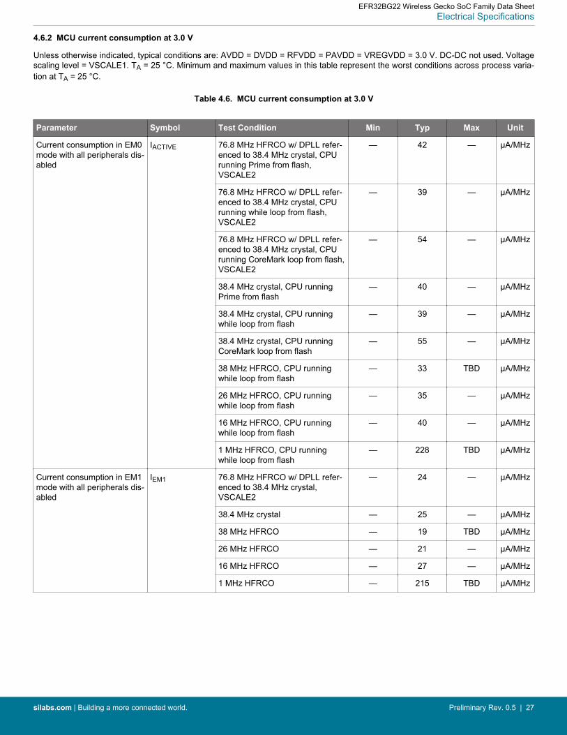
4.6.2 MCU current consumption at 3.0 V
Unless otherwise indicated, typical conditions are: AVDD = DVDD = RFVDD = PAVDD = VREGVDD = 3.0 V. DC-DC not used. Voltagescaling level = VSCALE1. TA = 25 °C. Minimum and maximum values in this table represent the worst conditions across process varia-tion at TA = 25 °C.
Table 4.6. MCU current consumption at 3.0 V
Parameter Symbol Test Condition Min Typ Max Unit
Current consumption in EM0mode with all peripherals dis-abled
IACTIVE 76.8 MHz HFRCO w/ DPLL refer-enced to 38.4 MHz crystal, CPUrunning Prime from flash,VSCALE2
— 42 — µA/MHz
76.8 MHz HFRCO w/ DPLL refer-enced to 38.4 MHz crystal, CPUrunning while loop from flash,VSCALE2
— 39 — µA/MHz
76.8 MHz HFRCO w/ DPLL refer-enced to 38.4 MHz crystal, CPUrunning CoreMark loop from flash,VSCALE2
— 54 — µA/MHz
38.4 MHz crystal, CPU runningPrime from flash
— 40 — µA/MHz
38.4 MHz crystal, CPU runningwhile loop from flash
— 39 — µA/MHz
38.4 MHz crystal, CPU runningCoreMark loop from flash
— 55 — µA/MHz
38 MHz HFRCO, CPU runningwhile loop from flash
— 33 TBD µA/MHz
26 MHz HFRCO, CPU runningwhile loop from flash
— 35 — µA/MHz
16 MHz HFRCO, CPU runningwhile loop from flash
— 40 — µA/MHz
1 MHz HFRCO, CPU runningwhile loop from flash
— 228 TBD µA/MHz
Current consumption in EM1mode with all peripherals dis-abled
IEM1 76.8 MHz HFRCO w/ DPLL refer-enced to 38.4 MHz crystal,VSCALE2
— 24 — µA/MHz
38.4 MHz crystal — 25 — µA/MHz
38 MHz HFRCO — 19 TBD µA/MHz
26 MHz HFRCO — 21 — µA/MHz
16 MHz HFRCO — 27 — µA/MHz
1 MHz HFRCO — 215 TBD µA/MHz
EFR32BG22 Wireless Gecko SoC Family Data SheetElectrical Specifications
silabs.com | Building a more connected world. Preliminary Rev. 0.5 | 27
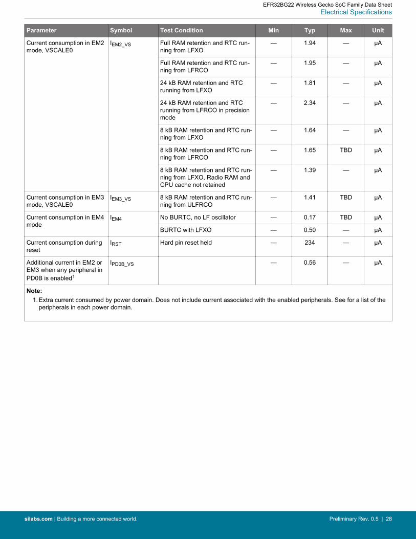
Parameter Symbol Test Condition Min Typ Max Unit
Current consumption in EM2mode, VSCALE0
IEM2_VS Full RAM retention and RTC run-ning from LFXO
— 1.94 — µA
Full RAM retention and RTC run-ning from LFRCO
— 1.95 — µA
24 kB RAM retention and RTCrunning from LFXO
— 1.81 — µA
24 kB RAM retention and RTCrunning from LFRCO in precisionmode
— 2.34 — µA
8 kB RAM retention and RTC run-ning from LFXO
— 1.64 — µA
8 kB RAM retention and RTC run-ning from LFRCO
— 1.65 TBD µA
8 kB RAM retention and RTC run-ning from LFXO, Radio RAM andCPU cache not retained
— 1.39 — µA
Current consumption in EM3mode, VSCALE0
IEM3_VS 8 kB RAM retention and RTC run-ning from ULFRCO
— 1.41 TBD µA
Current consumption in EM4mode
IEM4 No BURTC, no LF oscillator — 0.17 TBD µA
BURTC with LFXO — 0.50 — µA
Current consumption duringreset
IRST Hard pin reset held — 234 — µA
Additional current in EM2 orEM3 when any peripheral inPD0B is enabled1
IPD0B_VS — 0.56 — µA
Note:1. Extra current consumed by power domain. Does not include current associated with the enabled peripherals. See for a list of the
peripherals in each power domain.
EFR32BG22 Wireless Gecko SoC Family Data SheetElectrical Specifications
silabs.com | Building a more connected world. Preliminary Rev. 0.5 | 28
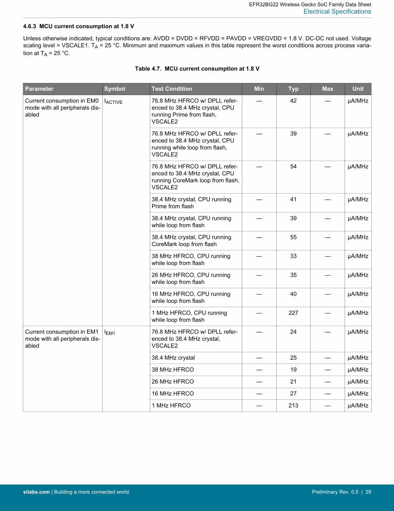
4.6.3 MCU current consumption at 1.8 V
Unless otherwise indicated, typical conditions are: AVDD = DVDD = RFVDD = PAVDD = VREGVDD = 1.8 V. DC-DC not used. Voltagescaling level = VSCALE1. TA = 25 °C. Minimum and maximum values in this table represent the worst conditions across process varia-tion at TA = 25 °C.
Table 4.7. MCU current consumption at 1.8 V
Parameter Symbol Test Condition Min Typ Max Unit
Current consumption in EM0mode with all peripherals dis-abled
IACTIVE 76.8 MHz HFRCO w/ DPLL refer-enced to 38.4 MHz crystal, CPUrunning Prime from flash,VSCALE2
— 42 — µA/MHz
76.8 MHz HFRCO w/ DPLL refer-enced to 38.4 MHz crystal, CPUrunning while loop from flash,VSCALE2
— 39 — µA/MHz
76.8 MHz HFRCO w/ DPLL refer-enced to 38.4 MHz crystal, CPUrunning CoreMark loop from flash,VSCALE2
— 54 — µA/MHz
38.4 MHz crystal, CPU runningPrime from flash
— 41 — µA/MHz
38.4 MHz crystal, CPU runningwhile loop from flash
— 39 — µA/MHz
38.4 MHz crystal, CPU runningCoreMark loop from flash
— 55 — µA/MHz
38 MHz HFRCO, CPU runningwhile loop from flash
— 33 — µA/MHz
26 MHz HFRCO, CPU runningwhile loop from flash
— 35 — µA/MHz
16 MHz HFRCO, CPU runningwhile loop from flash
— 40 — µA/MHz
1 MHz HFRCO, CPU runningwhile loop from flash
— 227 — µA/MHz
Current consumption in EM1mode with all peripherals dis-abled
IEM1 76.8 MHz HFRCO w/ DPLL refer-enced to 38.4 MHz crystal,VSCALE2
— 24 — µA/MHz
38.4 MHz crystal — 25 — µA/MHz
38 MHz HFRCO — 19 — µA/MHz
26 MHz HFRCO — 21 — µA/MHz
16 MHz HFRCO — 27 — µA/MHz
1 MHz HFRCO — 213 — µA/MHz
EFR32BG22 Wireless Gecko SoC Family Data SheetElectrical Specifications
silabs.com | Building a more connected world. Preliminary Rev. 0.5 | 29

Parameter Symbol Test Condition Min Typ Max Unit
Current consumption in EM2mode, VSCALE0
IEM2_VS Full RAM retention and RTC run-ning from LFXO
— 1.87 — µA
Full RAM retention and RTC run-ning from LFRCO
— 1.86 — µA
24 kB RAM retention and RTCrunning from LFXO
— 1.73 — µA
24 kB RAM retention and RTCrunning from LFRCO in precisionmode
— 2.26 — µA
8 kB RAM retention and RTC run-ning from LFXO
— 1.57 — µA
8 kB RAM retention and RTC run-ning from LFRCO
— 1.56 — µA
8 kB RAM retention and RTC run-ning from LFXO, Radio RAM andCPU cache not retained
— 1.32 — µA
Current consumption in EM3mode, VSCALE0
IEM3_VS 8 kB RAM retention and RTC run-ning from ULFRCO
— 1.34 — µA
Current consumption in EM4mode
IEM4 No BURTC, no LF oscillator — 0.13 — µA
BURTC with LFXO — 0.44 — µA
Current consumption duringreset
IRST Hard pin reset held — 190 — µA
Additional current in EM2 orEM3 when any peripheral inPD0B is enabled1
IPD0B_VS — 0.54 — µA
Note:1. Extra current consumed by power domain. Does not include current associated with the enabled peripherals. See for a list of the
peripherals in each power domain.
EFR32BG22 Wireless Gecko SoC Family Data SheetElectrical Specifications
silabs.com | Building a more connected world. Preliminary Rev. 0.5 | 30
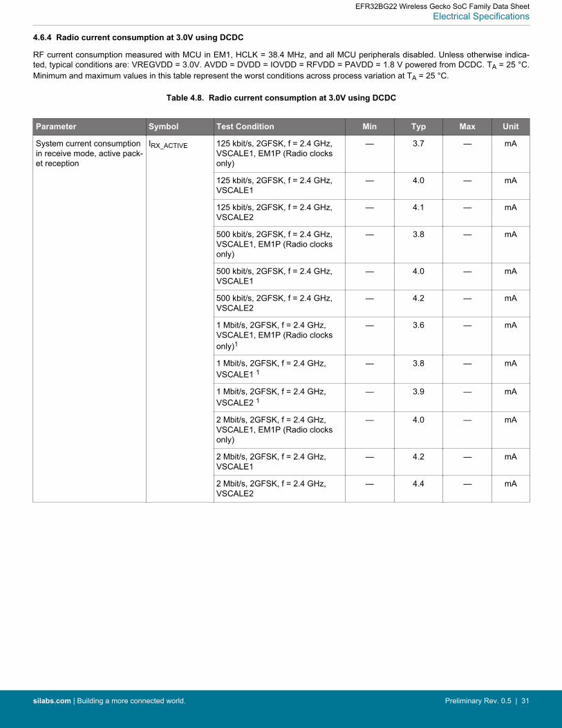
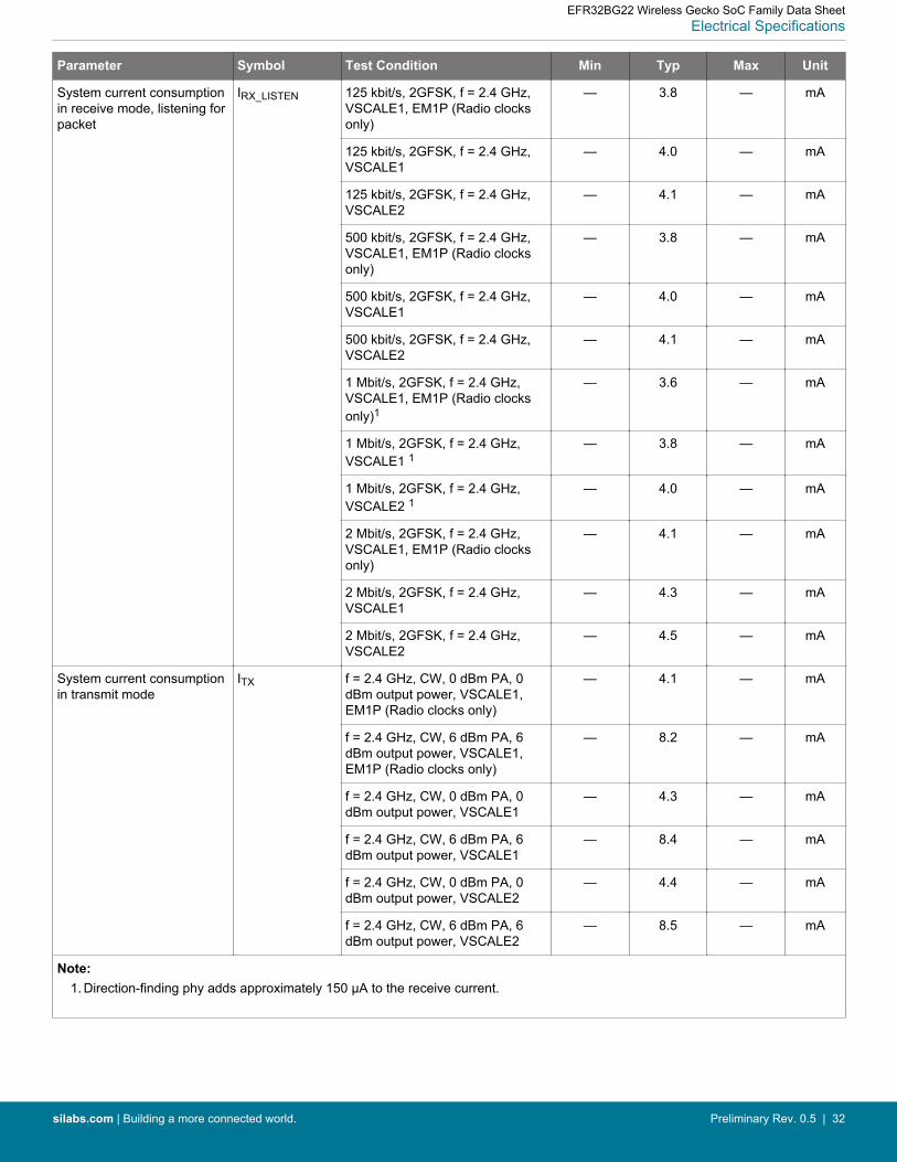
4.6.4 Radio current consumption at 3.0V using DCDC
RF current consumption measured with MCU in EM1, HCLK = 38.4 MHz, and all MCU peripherals disabled. Unless otherwise indica-ted, typical conditions are: VREGVDD = 3.0V. AVDD = DVDD = IOVDD = RFVDD = PAVDD = 1.8 V powered from DCDC. TA = 25 °C.Minimum and maximum values in this table represent the worst conditions across process variation at TA = 25 °C.
Table 4.8. Radio current consumption at 3.0V using DCDC
Parameter Symbol Test Condition Min Typ Max Unit
System current consumptionin receive mode, active pack-et reception
IRX_ACTIVE 125 kbit/s, 2GFSK, f = 2.4 GHz,VSCALE1, EM1P (Radio clocksonly)
— 3.7 — mA
125 kbit/s, 2GFSK, f = 2.4 GHz,VSCALE1
— 4.0 — mA
125 kbit/s, 2GFSK, f = 2.4 GHz,VSCALE2
— 4.1 — mA
500 kbit/s, 2GFSK, f = 2.4 GHz,VSCALE1, EM1P (Radio clocksonly)
— 3.8 — mA
500 kbit/s, 2GFSK, f = 2.4 GHz,VSCALE1
— 4.0 — mA
500 kbit/s, 2GFSK, f = 2.4 GHz,VSCALE2
— 4.2 — mA
1 Mbit/s, 2GFSK, f = 2.4 GHz,VSCALE1, EM1P (Radio clocksonly)1
— 3.6 — mA
1 Mbit/s, 2GFSK, f = 2.4 GHz,VSCALE1 1
— 3.8 — mA
1 Mbit/s, 2GFSK, f = 2.4 GHz,VSCALE2 1
— 3.9 — mA
2 Mbit/s, 2GFSK, f = 2.4 GHz,VSCALE1, EM1P (Radio clocksonly)
— 4.0 — mA
2 Mbit/s, 2GFSK, f = 2.4 GHz,VSCALE1
— 4.2 — mA
2 Mbit/s, 2GFSK, f = 2.4 GHz,VSCALE2
— 4.4 — mA
EFR32BG22 Wireless Gecko SoC Family Data SheetElectrical Specifications
silabs.com | Building a more connected world. Preliminary Rev. 0.5 | 31
Parameter Symbol Test Condition Min Typ Max Unit
System current consumptionin receive mode, listening forpacket
IRX_LISTEN 125 kbit/s, 2GFSK, f = 2.4 GHz,VSCALE1, EM1P (Radio clocksonly)
— 3.8 — mA
125 kbit/s, 2GFSK, f = 2.4 GHz,VSCALE1
— 4.0 — mA
125 kbit/s, 2GFSK, f = 2.4 GHz,VSCALE2
— 4.1 — mA
500 kbit/s, 2GFSK, f = 2.4 GHz,VSCALE1, EM1P (Radio clocksonly)
— 3.8 — mA
500 kbit/s, 2GFSK, f = 2.4 GHz,VSCALE1
— 4.0 — mA
500 kbit/s, 2GFSK, f = 2.4 GHz,VSCALE2
— 4.1 — mA
1 Mbit/s, 2GFSK, f = 2.4 GHz,VSCALE1, EM1P (Radio clocksonly)1
— 3.6 — mA
1 Mbit/s, 2GFSK, f = 2.4 GHz,VSCALE1 1
— 3.8 — mA
1 Mbit/s, 2GFSK, f = 2.4 GHz,VSCALE2 1
— 4.0 — mA
2 Mbit/s, 2GFSK, f = 2.4 GHz,VSCALE1, EM1P (Radio clocksonly)
— 4.1 — mA
2 Mbit/s, 2GFSK, f = 2.4 GHz,VSCALE1
— 4.3 — mA
2 Mbit/s, 2GFSK, f = 2.4 GHz,VSCALE2
— 4.5 — mA
System current consumptionin transmit mode
ITX f = 2.4 GHz, CW, 0 dBm PA, 0dBm output power, VSCALE1,EM1P (Radio clocks only)
— 4.1 — mA
f = 2.4 GHz, CW, 6 dBm PA, 6dBm output power, VSCALE1,EM1P (Radio clocks only)
— 8.2 — mA
f = 2.4 GHz, CW, 0 dBm PA, 0dBm output power, VSCALE1
— 4.3 — mA
f = 2.4 GHz, CW, 6 dBm PA, 6dBm output power, VSCALE1
— 8.4 — mA
f = 2.4 GHz, CW, 0 dBm PA, 0dBm output power, VSCALE2
— 4.4 — mA
f = 2.4 GHz, CW, 6 dBm PA, 6dBm output power, VSCALE2
— 8.5 — mA
Note:1. Direction-finding phy adds approximately 150 µA to the receive current.
EFR32BG22 Wireless Gecko SoC Family Data SheetElectrical Specifications
silabs.com | Building a more connected world. Preliminary Rev. 0.5 | 32
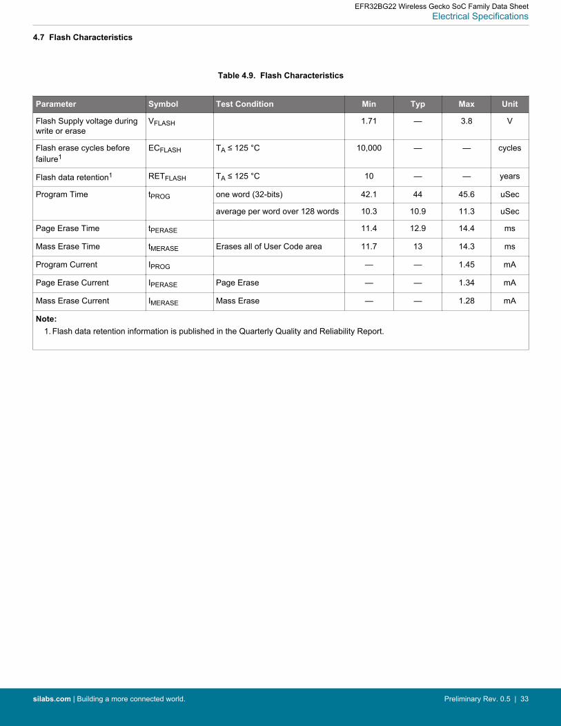
4.7 Flash Characteristics
Table 4.9. Flash Characteristics
Parameter Symbol Test Condition Min Typ Max Unit
Flash Supply voltage duringwrite or erase
VFLASH 1.71 — 3.8 V
Flash erase cycles beforefailure1
ECFLASH TA ≤ 125 °C 10,000 — — cycles
Flash data retention1 RETFLASH TA ≤ 125 °C 10 — — years
Program Time tPROG one word (32-bits) 42.1 44 45.6 uSec
average per word over 128 words 10.3 10.9 11.3 uSec
Page Erase Time tPERASE 11.4 12.9 14.4 ms
Mass Erase Time tMERASE Erases all of User Code area 11.7 13 14.3 ms
Program Current IPROG — — 1.45 mA
Page Erase Current IPERASE Page Erase — — 1.34 mA
Mass Erase Current IMERASE Mass Erase — — 1.28 mA
Note:1. Flash data retention information is published in the Quarterly Quality and Reliability Report.
EFR32BG22 Wireless Gecko SoC Family Data SheetElectrical Specifications
silabs.com | Building a more connected world. Preliminary Rev. 0.5 | 33
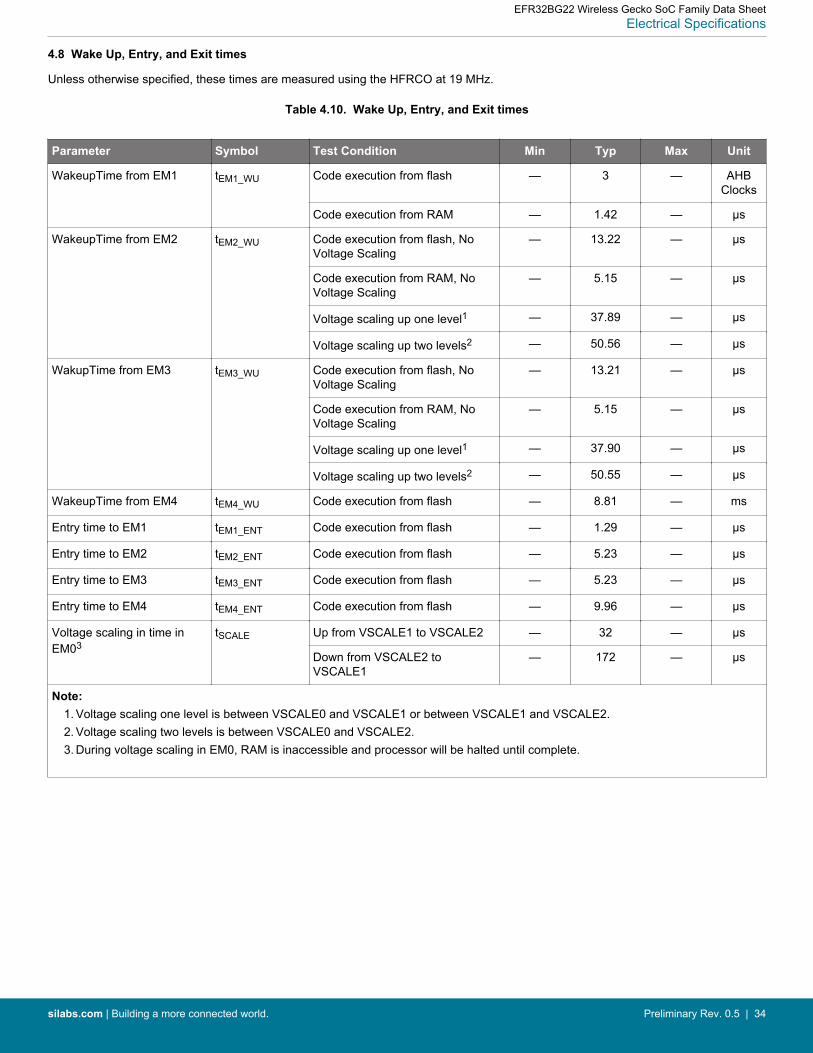
4.8 Wake Up, Entry, and Exit times
Unless otherwise specified, these times are measured using the HFRCO at 19 MHz.
Table 4.10. Wake Up, Entry, and Exit times
Parameter Symbol Test Condition Min Typ Max Unit
WakeupTime from EM1 tEM1_WU Code execution from flash — 3 — AHBClocks
Code execution from RAM — 1.42 — µs
WakeupTime from EM2 tEM2_WU Code execution from flash, NoVoltage Scaling
— 13.22 — µs
Code execution from RAM, NoVoltage Scaling
— 5.15 — µs
Voltage scaling up one level1 — 37.89 — µs
Voltage scaling up two levels2 — 50.56 — µs
WakupTime from EM3 tEM3_WU Code execution from flash, NoVoltage Scaling
— 13.21 — µs
Code execution from RAM, NoVoltage Scaling
— 5.15 — µs
Voltage scaling up one level1 — 37.90 — µs
Voltage scaling up two levels2 — 50.55 — µs
WakeupTime from EM4 tEM4_WU Code execution from flash — 8.81 — ms
Entry time to EM1 tEM1_ENT Code execution from flash — 1.29 — µs
Entry time to EM2 tEM2_ENT Code execution from flash — 5.23 — µs
Entry time to EM3 tEM3_ENT Code execution from flash — 5.23 — µs
Entry time to EM4 tEM4_ENT Code execution from flash — 9.96 — µs
Voltage scaling in time inEM03
tSCALE Up from VSCALE1 to VSCALE2 — 32 — µs
Down from VSCALE2 toVSCALE1
— 172 — µs
Note:1. Voltage scaling one level is between VSCALE0 and VSCALE1 or between VSCALE1 and VSCALE2.2. Voltage scaling two levels is between VSCALE0 and VSCALE2.3. During voltage scaling in EM0, RAM is inaccessible and processor will be halted until complete.
EFR32BG22 Wireless Gecko SoC Family Data SheetElectrical Specifications
silabs.com | Building a more connected world. Preliminary Rev. 0.5 | 34
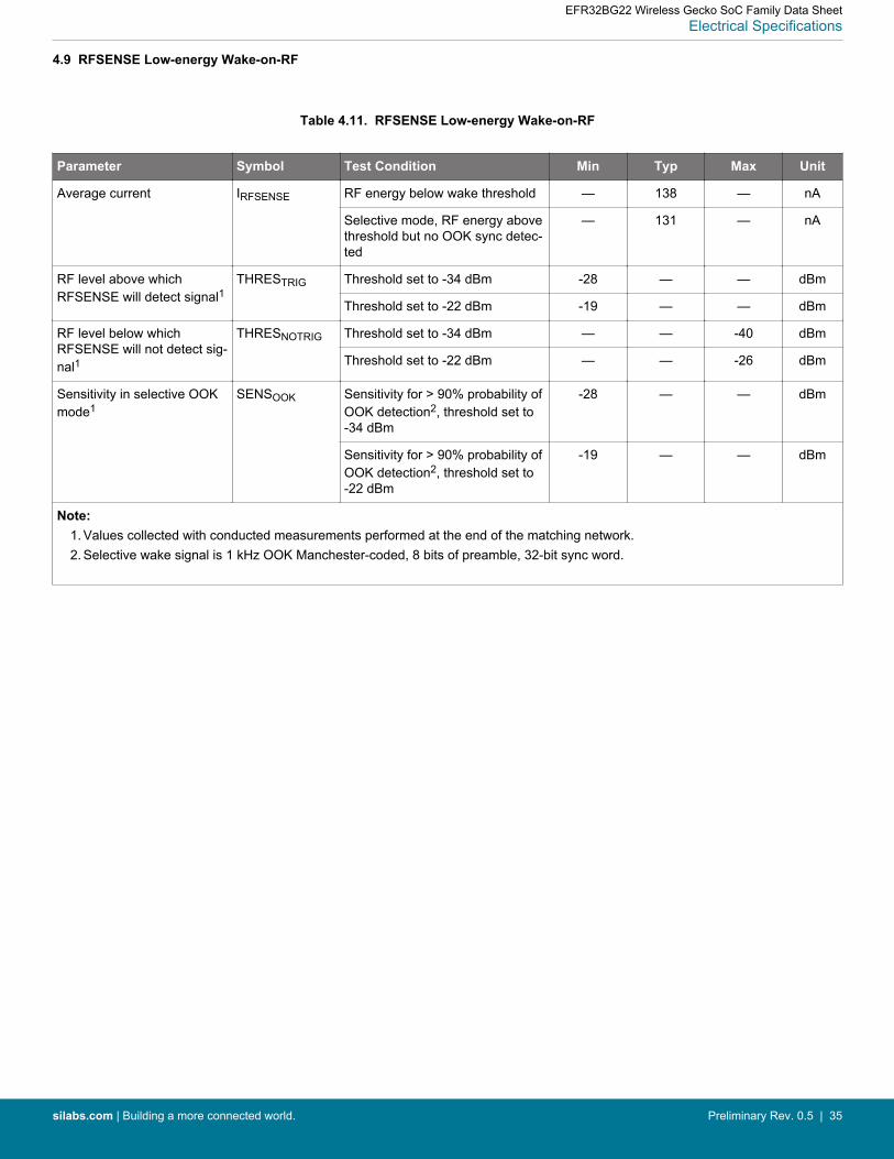
4.9 RFSENSE Low-energy Wake-on-RF
Table 4.11. RFSENSE Low-energy Wake-on-RF
Parameter Symbol Test Condition Min Typ Max Unit
Average current IRFSENSE RF energy below wake threshold — 138 — nA
Selective mode, RF energy abovethreshold but no OOK sync detec-ted
— 131 — nA
RF level above whichRFSENSE will detect signal1
THRESTRIG Threshold set to -34 dBm -28 — — dBm
Threshold set to -22 dBm -19 — — dBm
RF level below whichRFSENSE will not detect sig-nal1
THRESNOTRIG Threshold set to -34 dBm — — -40 dBm
Threshold set to -22 dBm — — -26 dBm
Sensitivity in selective OOKmode1
SENSOOK Sensitivity for > 90% probability ofOOK detection2, threshold set to-34 dBm
-28 — — dBm
Sensitivity for > 90% probability ofOOK detection2, threshold set to-22 dBm
-19 — — dBm
Note:1. Values collected with conducted measurements performed at the end of the matching network.2. Selective wake signal is 1 kHz OOK Manchester-coded, 8 bits of preamble, 32-bit sync word.
EFR32BG22 Wireless Gecko SoC Family Data SheetElectrical Specifications
silabs.com | Building a more connected world. Preliminary Rev. 0.5 | 35
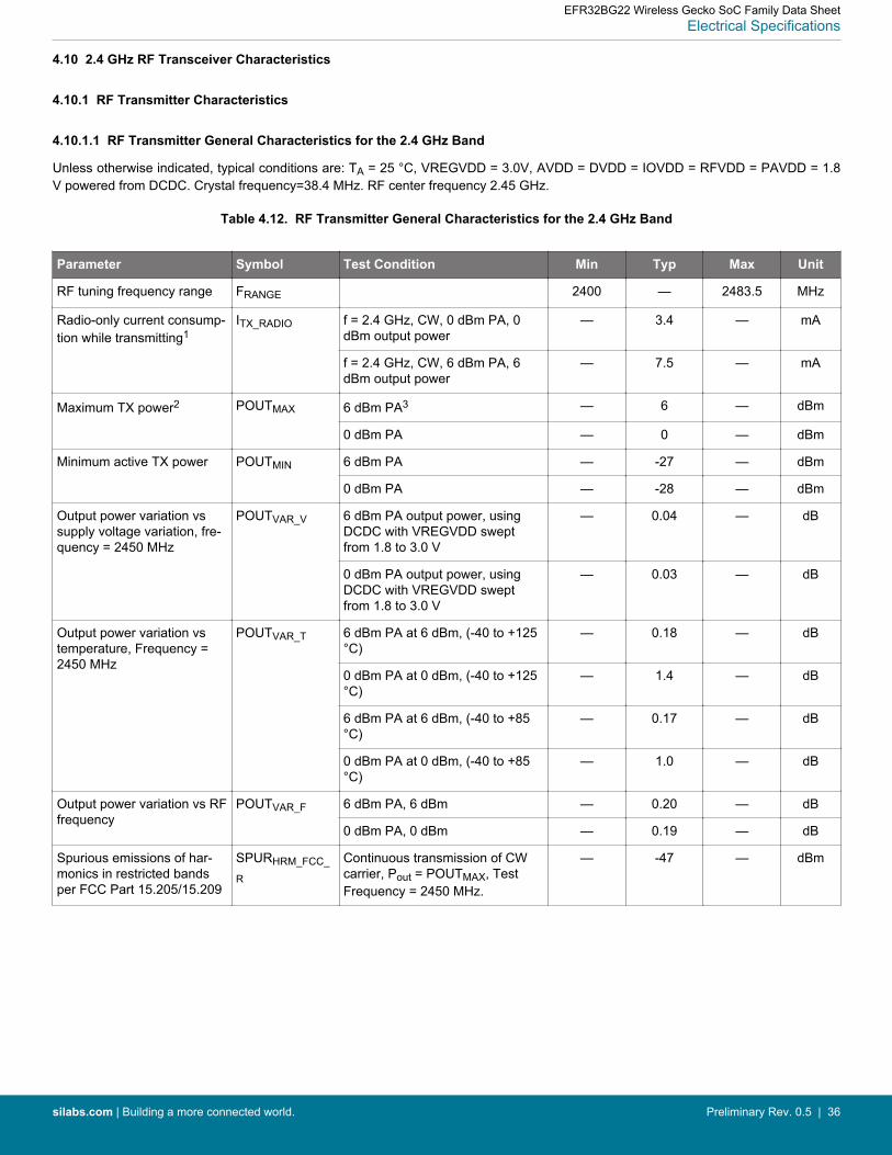
4.10 2.4 GHz RF Transceiver Characteristics
4.10.1 RF Transmitter Characteristics
4.10.1.1 RF Transmitter General Characteristics for the 2.4 GHz Band
Unless otherwise indicated, typical conditions are: TA = 25 °C, VREGVDD = 3.0V, AVDD = DVDD = IOVDD = RFVDD = PAVDD = 1.8V powered from DCDC. Crystal frequency=38.4 MHz. RF center frequency 2.45 GHz.
Table 4.12. RF Transmitter General Characteristics for the 2.4 GHz Band
Parameter Symbol Test Condition Min Typ Max Unit
RF tuning frequency range FRANGE 2400 — 2483.5 MHz
Radio-only current consump-tion while transmitting1
ITX_RADIO f = 2.4 GHz, CW, 0 dBm PA, 0dBm output power
— 3.4 — mA
f = 2.4 GHz, CW, 6 dBm PA, 6dBm output power
— 7.5 — mA
Maximum TX power2 POUTMAX 6 dBm PA3 — 6 — dBm
0 dBm PA — 0 — dBm
Minimum active TX power POUTMIN 6 dBm PA — -27 — dBm
0 dBm PA — -28 — dBm
Output power variation vssupply voltage variation, fre-quency = 2450 MHz
POUTVAR_V 6 dBm PA output power, usingDCDC with VREGVDD sweptfrom 1.8 to 3.0 V
— 0.04 — dB
0 dBm PA output power, usingDCDC with VREGVDD sweptfrom 1.8 to 3.0 V
— 0.03 — dB
Output power variation vstemperature, Frequency =2450 MHz
POUTVAR_T 6 dBm PA at 6 dBm, (-40 to +125°C)
— 0.18 — dB
0 dBm PA at 0 dBm, (-40 to +125°C)
— 1.4 — dB
6 dBm PA at 6 dBm, (-40 to +85°C)
— 0.17 — dB
0 dBm PA at 0 dBm, (-40 to +85°C)
— 1.0 — dB
Output power variation vs RFfrequency
POUTVAR_F 6 dBm PA, 6 dBm — 0.20 — dB
0 dBm PA, 0 dBm — 0.19 — dB
Spurious emissions of har-monics in restricted bandsper FCC Part 15.205/15.209
SPURHRM_FCC_
R
Continuous transmission of CWcarrier, Pout = POUTMAX, TestFrequency = 2450 MHz.
— -47 — dBm
EFR32BG22 Wireless Gecko SoC Family Data SheetElectrical Specifications
silabs.com | Building a more connected world. Preliminary Rev. 0.5 | 36
Parameter Symbol Test Condition Min Typ Max Unit
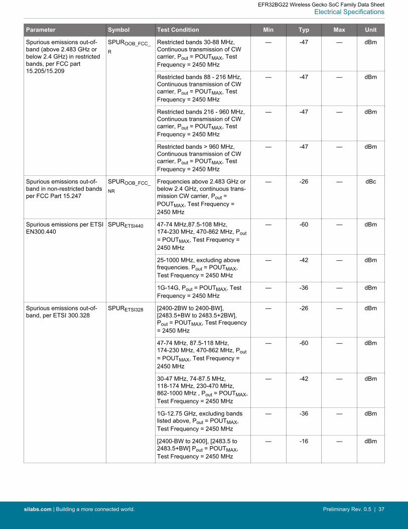
Spurious emissions out-of-band (above 2.483 GHz orbelow 2.4 GHz) in restrictedbands, per FCC part15.205/15.209
SPUROOB_FCC_
R
Restricted bands 30-88 MHz,Continuous transmission of CWcarrier, Pout = POUTMAX, TestFrequency = 2450 MHz
— -47 — dBm
Restricted bands 88 - 216 MHz,Continuous transmission of CWcarrier, Pout = POUTMAX, TestFrequency = 2450 MHz
— -47 — dBm
Restricted bands 216 - 960 MHz,Continuous transmission of CWcarrier, Pout = POUTMAX, TestFrequency = 2450 MHz
— -47 — dBm
Restricted bands > 960 MHz,Continuous transmission of CWcarrier, Pout = POUTMAX, TestFrequency = 2450 MHz
— -47 — dBm
Spurious emissions out-of-band in non-restricted bandsper FCC Part 15.247
SPUROOB_FCC_
NR
Frequencies above 2.483 GHz orbelow 2.4 GHz, continuous trans-mission CW carrier, Pout =POUTMAX, Test Frequency =2450 MHz
— -26 — dBc
Spurious emissions per ETSIEN300.440
SPURETSI440 47-74 MHz,87.5-108 MHz,174-230 MHz, 470-862 MHz, Pout= POUTMAX, Test Frequency =2450 MHz
— -60 — dBm
25-1000 MHz, excluding abovefrequencies. Pout = POUTMAX,Test Frequency = 2450 MHz
— -42 — dBm
1G-14G, Pout = POUTMAX, TestFrequency = 2450 MHz
— -36 — dBm
Spurious emissions out-of-band, per ETSI 300.328
SPURETSI328 [2400-2BW to 2400-BW],[2483.5+BW to 2483.5+2BW],Pout = POUTMAX, Test Frequency= 2450 MHz
— -26 — dBm
47-74 MHz, 87.5-118 MHz,174-230 MHz, 470-862 MHz, Pout= POUTMAX, Test Frequency =2450 MHz
— -60 — dBm
30-47 MHz, 74-87.5 MHz,118-174 MHz, 230-470 MHz,862-1000 MHz , Pout = POUTMAX,Test Frequency = 2450 MHz
— -42 — dBm
1G-12.75 GHz, excluding bandslisted above, Pout = POUTMAX,Test Frequency = 2450 MHz
— -36 — dBm
[2400-BW to 2400], [2483.5 to2483.5+BW] Pout = POUTMAX,Test Frequency = 2450 MHz
— -16 — dBm
EFR32BG22 Wireless Gecko SoC Family Data SheetElectrical Specifications
silabs.com | Building a more connected world. Preliminary Rev. 0.5 | 37
Parameter Symbol Test Condition Min Typ Max Unit
Note:1. Supply current to radio, supplied by DC-DC with 3.0 V, measured at VREGVDD.2. Supported transmit power levels are determined by the ordering part number (OPN). Transmit power ratings for all devices cov-
ered in this data sheet can be found in the Max TX Power column of the Ordering Information Table.3. The PA is capable of delivering higher than 6 dBm output power (see Figure 4.9 Transmitter Output Power on page 71. Howev-
er, all transmitter characteristics and recommended application circuits are specified at 6 dBm output. If used with the recommen-ded application circuits above 6 dBm, harmonics may be higher than regulatory limits.
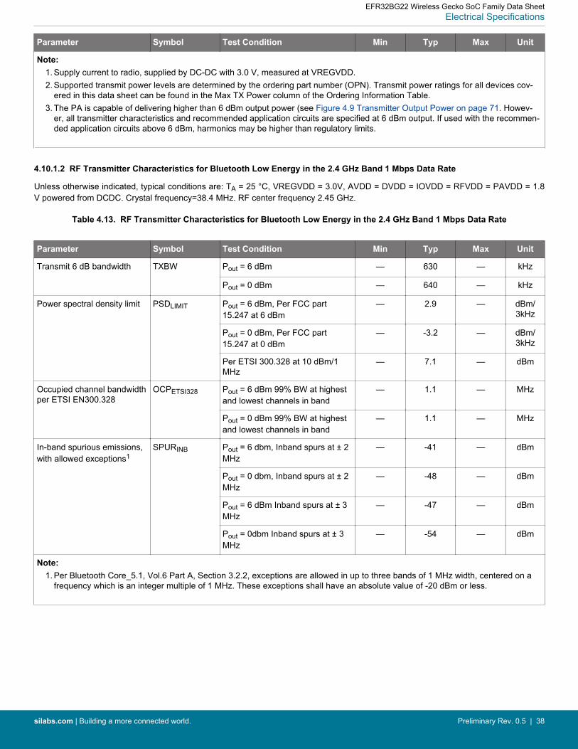
4.10.1.2 RF Transmitter Characteristics for Bluetooth Low Energy in the 2.4 GHz Band 1 Mbps Data Rate
Unless otherwise indicated, typical conditions are: TA = 25 °C, VREGVDD = 3.0V, AVDD = DVDD = IOVDD = RFVDD = PAVDD = 1.8V powered from DCDC. Crystal frequency=38.4 MHz. RF center frequency 2.45 GHz.
Table 4.13. RF Transmitter Characteristics for Bluetooth Low Energy in the 2.4 GHz Band 1 Mbps Data Rate
Parameter Symbol Test Condition Min Typ Max Unit
Transmit 6 dB bandwidth TXBW Pout = 6 dBm — 630 — kHz
Pout = 0 dBm — 640 — kHz
Power spectral density limit PSDLIMIT Pout = 6 dBm, Per FCC part15.247 at 6 dBm
— 2.9 — dBm/3kHz
Pout = 0 dBm, Per FCC part15.247 at 0 dBm
— -3.2 — dBm/3kHz
Per ETSI 300.328 at 10 dBm/1MHz
— 7.1 — dBm
Occupied channel bandwidthper ETSI EN300.328
OCPETSI328 Pout = 6 dBm 99% BW at highestand lowest channels in band
— 1.1 — MHz
Pout = 0 dBm 99% BW at highestand lowest channels in band
— 1.1 — MHz
In-band spurious emissions,with allowed exceptions1
SPURINB Pout = 6 dbm, Inband spurs at ± 2MHz
— -41 — dBm
Pout = 0 dbm, Inband spurs at ± 2MHz
— -48 — dBm
Pout = 6 dBm Inband spurs at ± 3MHz
— -47 — dBm
Pout = 0dbm Inband spurs at ± 3MHz
— -54 — dBm
Note:1. Per Bluetooth Core_5.1, Vol.6 Part A, Section 3.2.2, exceptions are allowed in up to three bands of 1 MHz width, centered on a
frequency which is an integer multiple of 1 MHz. These exceptions shall have an absolute value of -20 dBm or less.
EFR32BG22 Wireless Gecko SoC Family Data SheetElectrical Specifications
silabs.com | Building a more connected world. Preliminary Rev. 0.5 | 38
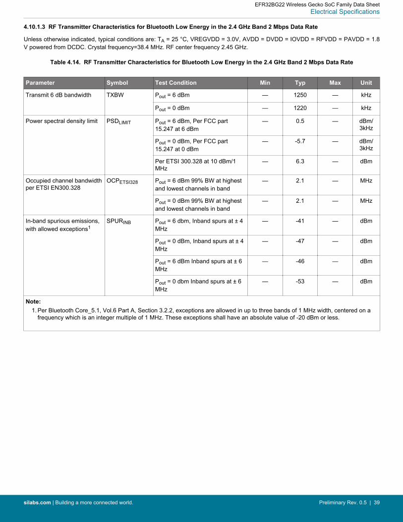
4.10.1.3 RF Transmitter Characteristics for Bluetooth Low Energy in the 2.4 GHz Band 2 Mbps Data Rate
Unless otherwise indicated, typical conditions are: TA = 25 °C, VREGVDD = 3.0V, AVDD = DVDD = IOVDD = RFVDD = PAVDD = 1.8V powered from DCDC. Crystal frequency=38.4 MHz. RF center frequency 2.45 GHz.
Table 4.14. RF Transmitter Characteristics for Bluetooth Low Energy in the 2.4 GHz Band 2 Mbps Data Rate
Parameter Symbol Test Condition Min Typ Max Unit
Transmit 6 dB bandwidth TXBW Pout = 6 dBm — 1250 — kHz
Pout = 0 dBm — 1220 — kHz
Power spectral density limit PSDLIMIT Pout = 6 dBm, Per FCC part15.247 at 6 dBm
— 0.5 — dBm/3kHz
Pout = 0 dBm, Per FCC part15.247 at 0 dBm
— -5.7 — dBm/3kHz
Per ETSI 300.328 at 10 dBm/1MHz
— 6.3 — dBm
Occupied channel bandwidthper ETSI EN300.328
OCPETSI328 Pout = 6 dBm 99% BW at highestand lowest channels in band
— 2.1 — MHz
Pout = 0 dBm 99% BW at highestand lowest channels in band
— 2.1 — MHz
In-band spurious emissions,with allowed exceptions1
SPURINB Pout = 6 dbm, Inband spurs at ± 4MHz
— -41 — dBm
Pout = 0 dBm, Inband spurs at ± 4MHz
— -47 — dBm
Pout = 6 dBm Inband spurs at ± 6MHz
— -46 — dBm
Pout = 0 dbm Inband spurs at ± 6MHz
— -53 — dBm
Note:1. Per Bluetooth Core_5.1, Vol.6 Part A, Section 3.2.2, exceptions are allowed in up to three bands of 1 MHz width, centered on a
frequency which is an integer multiple of 1 MHz. These exceptions shall have an absolute value of -20 dBm or less.
EFR32BG22 Wireless Gecko SoC Family Data SheetElectrical Specifications
silabs.com | Building a more connected world. Preliminary Rev. 0.5 | 39

4.10.1.4 RF Transmitter Characteristics for Bluetooth Low Energy in the 2.4 GHz Band 500 kbps Data Rate
Unless otherwise indicated, typical conditions are: TA = 25 °C, VREGVDD = 3.0V, AVDD = DVDD = IOVDD = RFVDD = PAVDD = 1.8V powered from DCDC. Crystal frequency=38.4 MHz. RF center frequency 2.45 GHz.
Table 4.15. RF Transmitter Characteristics for Bluetooth Low Energy in the 2.4 GHz Band 500 kbps Data Rate
Parameter Symbol Test Condition Min Typ Max Unit
Transmit 6 dB bandwidth TXBW Pout = 6 dBm — 640 — kHz
Pout = 0 dBm — 650 — kHz
Power spectral density limit PSDLIMIT Pout = 6 dBm, Per FCC part15.247 at 6 dBm
— 2.8 — dBm/3kHz
Pout = 0 dBm, Per FCC part15.247 at 0 dBm
— -3.5 — dBm/3kHz
Per ETSI 300.328 at 10 dBm/1MHz
— 7.1 — dBm
Occupied channel bandwidthper ETSI EN300.328
OCPETSI328 Pout = 6 dBm 99% BW at highestand lowest channels in band
— 1.1 — MHz
Pout = 0 dBm 99% BW at highestand lowest channels in band
— 1.1 — MHz
In-band spurious emissions,with allowed exceptions1
SPURINB Pout = 6 dbm, Inband spurs at ± 2MHz
— -41 — dBm
Pout = 0 dbm, Inband spurs at ± 2MHz
— -48 — dBm
Pout = 6 dBm Inband spurs at ± 3MHz
— -47 — dBm
Pout = 0dbm Inband spurs at ± 3MHz
— -54 — dBm
Note:1. Per Bluetooth Core_5.1, Vol.6 Part A, Section 3.2.2, exceptions are allowed in up to three bands of 1 MHz width, centered on a
frequency which is an integer multiple of 1 MHz. These exceptions shall have an absolute value of -20 dBm or less.
EFR32BG22 Wireless Gecko SoC Family Data SheetElectrical Specifications
silabs.com | Building a more connected world. Preliminary Rev. 0.5 | 40

4.10.1.5 RF Transmitter Characteristics for Bluetooth Low Energy in the 2.4 GHz Band 125 kbps Data Rate
Unless otherwise indicated, typical conditions are: TA = 25 °C, VREGVDD = 3.0V, AVDD = DVDD = IOVDD = RFVDD = PAVDD = 1.8V powered from DCDC. Crystal frequency=38.4 MHz. RF center frequency 2.45 GHz.
Table 4.16. RF Transmitter Characteristics for Bluetooth Low Energy in the 2.4 GHz Band 125 kbps Data Rate
Parameter Symbol Test Condition Min Typ Max Unit
Transmit 6 dB bandwidth TXBW Pout = 6 dBm — 600 — kHz
Pout = 0 dBm — 600 — kHz
Power spectral density limit PSDLIMIT Pout = 6 dBm, Per FCC part15.247 at 6 dBm
— 2.0 — dBm/3kHz
Pout = 0 dBm, Per FCC part15.247 at 0 dBm
— -4.2 — dBm/3kHz
Per ETSI 300.328 at 10 dBm/1MHz
— 7.1 — dBm
Occupied channel bandwidthper ETSI EN300.328
OCPETSI328 Pout = 6 dBm 99% BW at highestand lowest channels in band
— 1.1 — MHz
Pout = 0 dBm 99% BW at highestand lowest channels in band
— 1.1 — MHz
In-band spurious emissions,with allowed exceptions1
SPURINB Pout = 6 dbm, Inband spurs at ± 2MHz
— -41 — dBm
Pout = 0 dbm, Inband spurs at ± 2MHz
— -47 — dBm
Pout = 6 dBm Inband spurs at ± 3MHz
— -47 — dBm
Pout = 0dbm Inband spurs at ± 3MHz
— -54 — dBm
Note:1. Per Bluetooth Core_5.1, Vol.6 Part A, Section 3.2.2, exceptions are allowed in up to three bands of 1 MHz width, centered on a
frequency which is an integer multiple of 1 MHz. These exceptions shall have an absolute value of -20 dBm or less.
EFR32BG22 Wireless Gecko SoC Family Data SheetElectrical Specifications
silabs.com | Building a more connected world. Preliminary Rev. 0.5 | 41
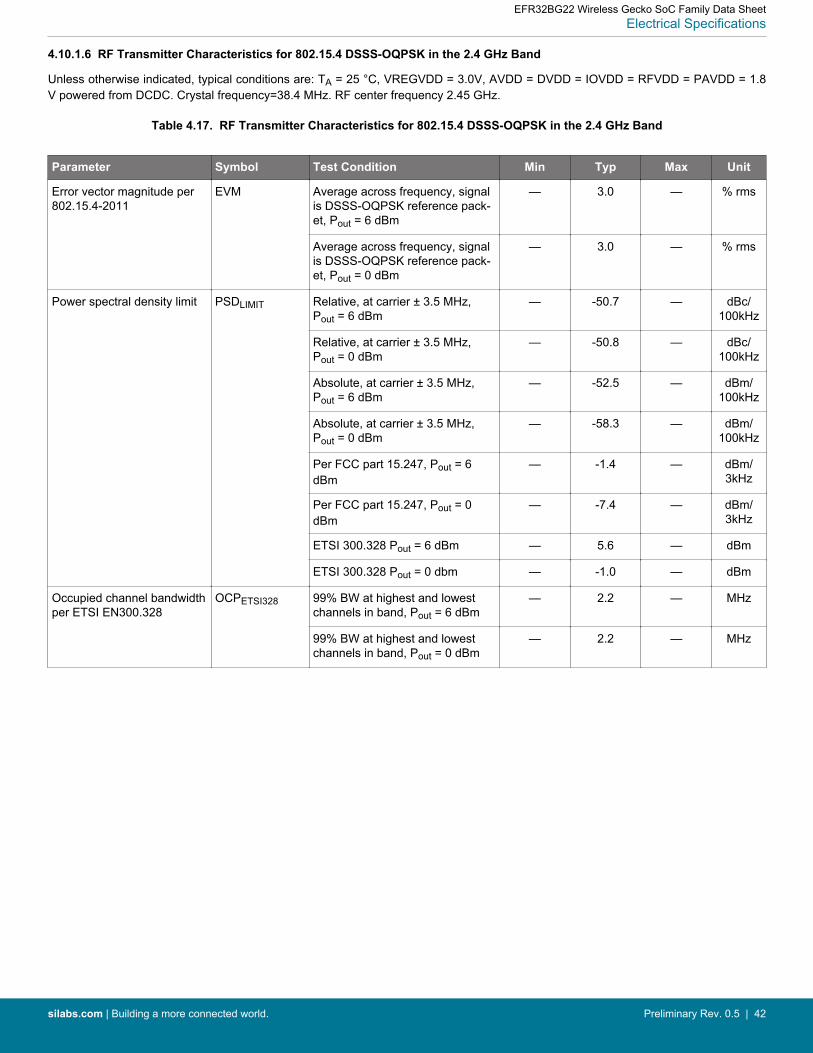
4.10.1.6 RF Transmitter Characteristics for 802.15.4 DSSS-OQPSK in the 2.4 GHz Band
Unless otherwise indicated, typical conditions are: TA = 25 °C, VREGVDD = 3.0V, AVDD = DVDD = IOVDD = RFVDD = PAVDD = 1.8V powered from DCDC. Crystal frequency=38.4 MHz. RF center frequency 2.45 GHz.
Table 4.17. RF Transmitter Characteristics for 802.15.4 DSSS-OQPSK in the 2.4 GHz Band
Parameter Symbol Test Condition Min Typ Max Unit
Error vector magnitude per802.15.4-2011
EVM Average across frequency, signalis DSSS-OQPSK reference pack-et, Pout = 6 dBm
— 3.0 — % rms
Average across frequency, signalis DSSS-OQPSK reference pack-et, Pout = 0 dBm
— 3.0 — % rms
Power spectral density limit PSDLIMIT Relative, at carrier ± 3.5 MHz,Pout = 6 dBm
— -50.7 — dBc/100kHz
Relative, at carrier ± 3.5 MHz,Pout = 0 dBm
— -50.8 — dBc/100kHz
Absolute, at carrier ± 3.5 MHz,Pout = 6 dBm
— -52.5 — dBm/100kHz
Absolute, at carrier ± 3.5 MHz,Pout = 0 dBm
— -58.3 — dBm/100kHz
Per FCC part 15.247, Pout = 6dBm
— -1.4 — dBm/3kHz
Per FCC part 15.247, Pout = 0dBm
— -7.4 — dBm/3kHz
ETSI 300.328 Pout = 6 dBm — 5.6 — dBm
ETSI 300.328 Pout = 0 dbm — -1.0 — dBm
Occupied channel bandwidthper ETSI EN300.328
OCPETSI328 99% BW at highest and lowestchannels in band, Pout = 6 dBm
— 2.2 — MHz
99% BW at highest and lowestchannels in band, Pout = 0 dBm
— 2.2 — MHz
EFR32BG22 Wireless Gecko SoC Family Data SheetElectrical Specifications
silabs.com | Building a more connected world. Preliminary Rev. 0.5 | 42
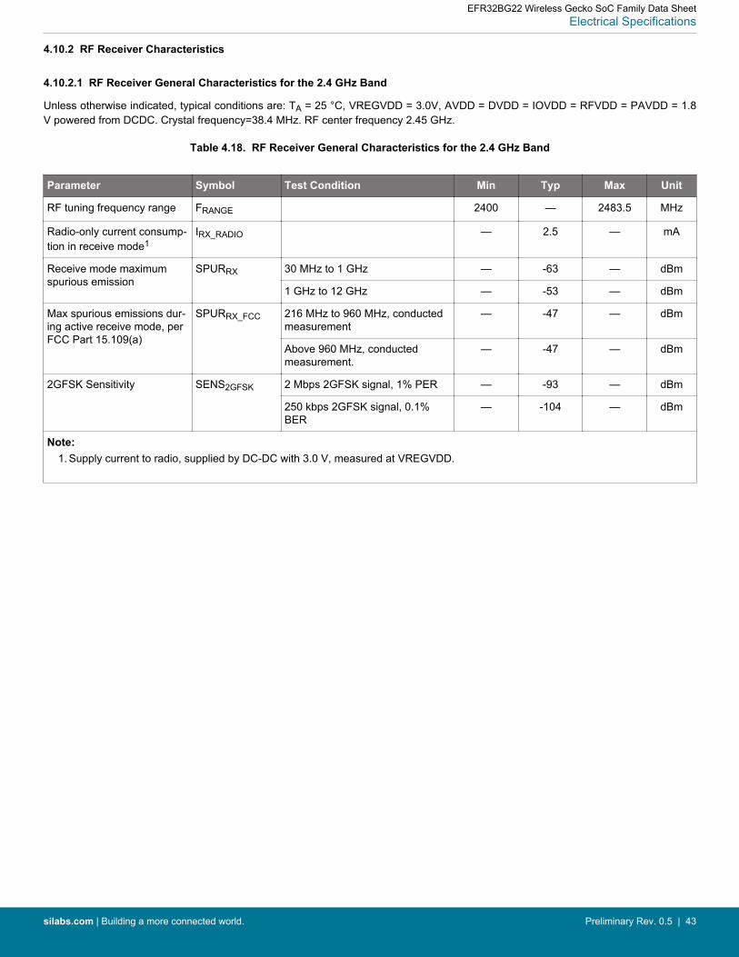
4.10.2 RF Receiver Characteristics
4.10.2.1 RF Receiver General Characteristics for the 2.4 GHz Band
Unless otherwise indicated, typical conditions are: TA = 25 °C, VREGVDD = 3.0V, AVDD = DVDD = IOVDD = RFVDD = PAVDD = 1.8V powered from DCDC. Crystal frequency=38.4 MHz. RF center frequency 2.45 GHz.
Table 4.18. RF Receiver General Characteristics for the 2.4 GHz Band
Parameter Symbol Test Condition Min Typ Max Unit
RF tuning frequency range FRANGE 2400 — 2483.5 MHz
Radio-only current consump-tion in receive mode1
IRX_RADIO — 2.5 — mA
Receive mode maximumspurious emission
SPURRX 30 MHz to 1 GHz — -63 — dBm
1 GHz to 12 GHz — -53 — dBm
Max spurious emissions dur-ing active receive mode, perFCC Part 15.109(a)
SPURRX_FCC 216 MHz to 960 MHz, conductedmeasurement
— -47 — dBm
Above 960 MHz, conductedmeasurement.
— -47 — dBm
2GFSK Sensitivity SENS2GFSK 2 Mbps 2GFSK signal, 1% PER — -93 — dBm
250 kbps 2GFSK signal, 0.1%BER
— -104 — dBm
Note:1. Supply current to radio, supplied by DC-DC with 3.0 V, measured at VREGVDD.
EFR32BG22 Wireless Gecko SoC Family Data SheetElectrical Specifications
silabs.com | Building a more connected world. Preliminary Rev. 0.5 | 43
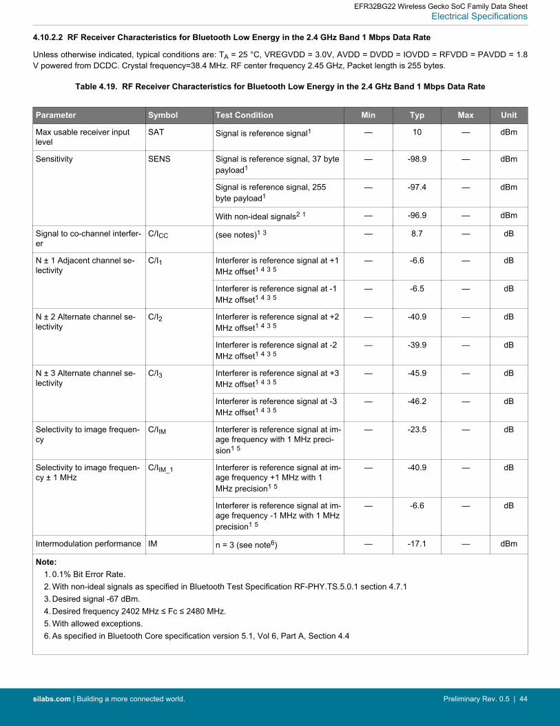
4.10.2.2 RF Receiver Characteristics for Bluetooth Low Energy in the 2.4 GHz Band 1 Mbps Data Rate
Unless otherwise indicated, typical conditions are: TA = 25 °C, VREGVDD = 3.0V, AVDD = DVDD = IOVDD = RFVDD = PAVDD = 1.8V powered from DCDC. Crystal frequency=38.4 MHz. RF center frequency 2.45 GHz, Packet length is 255 bytes.
Table 4.19. RF Receiver Characteristics for Bluetooth Low Energy in the 2.4 GHz Band 1 Mbps Data Rate
Parameter Symbol Test Condition Min Typ Max Unit
Max usable receiver inputlevel
SAT Signal is reference signal1 — 10 — dBm
Sensitivity SENS Signal is reference signal, 37 bytepayload1
— -98.9 — dBm
Signal is reference signal, 255byte payload1
— -97.4 — dBm
With non-ideal signals2 1 — -96.9 — dBm
Signal to co-channel interfer-er
C/ICC (see notes)1 3 — 8.7 — dB
N ± 1 Adjacent channel se-lectivity
C/I1 Interferer is reference signal at +1MHz offset1 4 3 5
— -6.6 — dB
Interferer is reference signal at -1MHz offset1 4 3 5
— -6.5 — dB
N ± 2 Alternate channel se-lectivity
C/I2 Interferer is reference signal at +2MHz offset1 4 3 5
— -40.9 — dB
Interferer is reference signal at -2MHz offset1 4 3 5
— -39.9 — dB
N ± 3 Alternate channel se-lectivity
C/I3 Interferer is reference signal at +3MHz offset1 4 3 5
— -45.9 — dB
Interferer is reference signal at -3MHz offset1 4 3 5
— -46.2 — dB
Selectivity to image frequen-cy
C/IIM Interferer is reference signal at im-age frequency with 1 MHz preci-sion1 5
— -23.5 — dB
Selectivity to image frequen-cy ± 1 MHz
C/IIM_1 Interferer is reference signal at im-age frequency +1 MHz with 1MHz precision1 5
— -40.9 — dB
Interferer is reference signal at im-age frequency -1 MHz with 1 MHzprecision1 5
— -6.6 — dB
Intermodulation performance IM n = 3 (see note6) — -17.1 — dBm
Note:1. 0.1% Bit Error Rate.2. With non-ideal signals as specified in Bluetooth Test Specification RF-PHY.TS.5.0.1 section 4.7.13. Desired signal -67 dBm.4. Desired frequency 2402 MHz ≤ Fc ≤ 2480 MHz.5. With allowed exceptions.6. As specified in Bluetooth Core specification version 5.1, Vol 6, Part A, Section 4.4
EFR32BG22 Wireless Gecko SoC Family Data SheetElectrical Specifications
silabs.com | Building a more connected world. Preliminary Rev. 0.5 | 44

4.10.2.3 RF Receiver Characteristics for Bluetooth Low Energy in the 2.4 GHz Band 2 Mbps Data Rate
Unless otherwise indicated, typical conditions are: TA = 25 °C, VREGVDD = 3.0V, AVDD = DVDD = IOVDD = RFVDD = PAVDD = 1.8V powered from DCDC. Crystal frequency=38.4 MHz. RF center frequency 2.45 GHz, Packet length is 255 bytes.
Table 4.20. RF Receiver Characteristics for Bluetooth Low Energy in the 2.4 GHz Band 2 Mbps Data Rate
Parameter Symbol Test Condition Min Typ Max Unit
Max usable receiver inputlevel
SAT Signal is reference signal1 — 10 — dBm
Sensitivity SENS Signal is reference signal, 37 bytepayload1
— -96.2 — dBm
Signal is reference signal, 255byte payload1
— -94.6 — dBm
With non-ideal signals2 1 — -94.4 — dBm
Signal to co-channel interfer-er
C/ICC (see notes)1 3 — 8.8 — dB
N ± 1 Adjacent channel se-lectivity
C/I1 Interferer is reference signal at +2MHz offset1 4 3 5
— -9.2 — dB
Interferer is reference signal at -2MHz offset1 4 3 5
— -6.6 — dB
N ± 2 Alternate channel se-lectivity
C/I2 Interferer is reference signal at +4MHz offset1 4 3 5
— -43.3 — dB
Interferer is reference signal at -4MHz offset1 4 3 5
— -44.0 — dB
N ± 3 Alternate channel se-lectivity
C/I3 Interferer is reference signal at +6MHz offset1 4 3 5
— -48.6 — dB
Interferer is reference signal at -6MHz offset1 4 3 5
— -50.7 — dB
Selectivity to image frequen-cy
C/IIM Interferer is reference signal at im-age frequency with 1 MHz preci-sion1 5
— -23.8 — dB
Selectivity to image frequen-cy ± 2 MHz
C/IIM_1 Interferer is reference signal at im-age frequency +2 MHz with 1MHz precision1 5
— -43.3 — dB
Interferer is reference signal at im-age frequency -2 MHz with 1 MHzprecision1 5
— -9.2 — dB
Intermodulation performance IM n = 3 (see note6) — -18.8 — dBm
Note:1. 0.1% Bit Error Rate.2. With non-ideal signals as specified in Bluetooth Test Specification RF-PHY.TS.5.0.1 section 4.7.13. Desired signal -64 dBm.4. Desired frequency 2402 MHz ≤ Fc ≤ 2480 MHz.5. With allowed exceptions.6. As specified in Bluetooth Core specification version 5.1, Vol 6, Part A, Section 4.4
EFR32BG22 Wireless Gecko SoC Family Data SheetElectrical Specifications
silabs.com | Building a more connected world. Preliminary Rev. 0.5 | 45

4.10.2.4 RF Receiver Characteristics for Bluetooth Low Energy in the 2.4 GHz Band 500 kbps Data Rate
Unless otherwise indicated, typical conditions are: TA = 25 °C, VREGVDD = 3.0V, AVDD = DVDD = IOVDD = RFVDD = PAVDD = 1.8V powered from DCDC. Crystal frequency=38.4 MHz. RF center frequency 2.45 GHz, Packet length is 255 bytes.
Table 4.21. RF Receiver Characteristics for Bluetooth Low Energy in the 2.4 GHz Band 500 kbps Data Rate
Parameter Symbol Test Condition Min Typ Max Unit
Max usable receiver inputlevel
SAT Signal is reference signal1 — 10 — dBm
Sensitivity SENS Signal is reference signal, 37 bytepayload1
— -102.5 — dBm
Signal is reference signal, 255byte payload1
— -101.2 — dBm
With non-ideal signals2 1 — -100.2 — dBm
Signal to co-channel interfer-er
C/ICC (see notes)1 3 — 2.7 — dB
N ± 1 Adjacent channel se-lectivity
C/I1 Interferer is reference signal at +1MHz offset1 4 3 5
— -8.0 — dB
Interferer is reference signal at -1MHz offset1 4 3 5
— -7.9 — dB
N ± 2 Alternate channel se-lectivity
C/I2 Interferer is reference signal at +2MHz offset1 4 3 5
— -46.5 — dB
Interferer is reference signal at -2MHz offset1 4 3 5
— -49.9 — dB
N ± 3 Alternate channel se-lectivity
C/I3 Interferer is reference signal at +3MHz offset1 4 3 5
— -48.9 — dB
Interferer is reference signal at -3MHz offset1 4 3 5
— -53.8 — dB
Selectivity to image frequen-cy
C/IIM Interferer is reference signal at im-age frequency with 1 MHz preci-sion1 5
— -48.3 — dB
Selectivity to image frequen-cy ± 1 MHz
C/IIM_1 Interferer is reference signal at im-age frequency +1 MHz with 1MHz precision1 5
— -49.9 — dB
Interferer is reference signal at im-age frequency -1 MHz with 1 MHzprecision1 5
— -46.5 — dB
Note:1. 0.1% Bit Error Rate.2. With non-ideal signals as specified in Bluetooth Test Specification RF-PHY.TS.5.0.1 section 4.7.13. Desired signal -72 dBm.4. Desired frequency 2402 MHz ≤ Fc ≤ 2480 MHz.5. With allowed exceptions.
EFR32BG22 Wireless Gecko SoC Family Data SheetElectrical Specifications
silabs.com | Building a more connected world. Preliminary Rev. 0.5 | 46
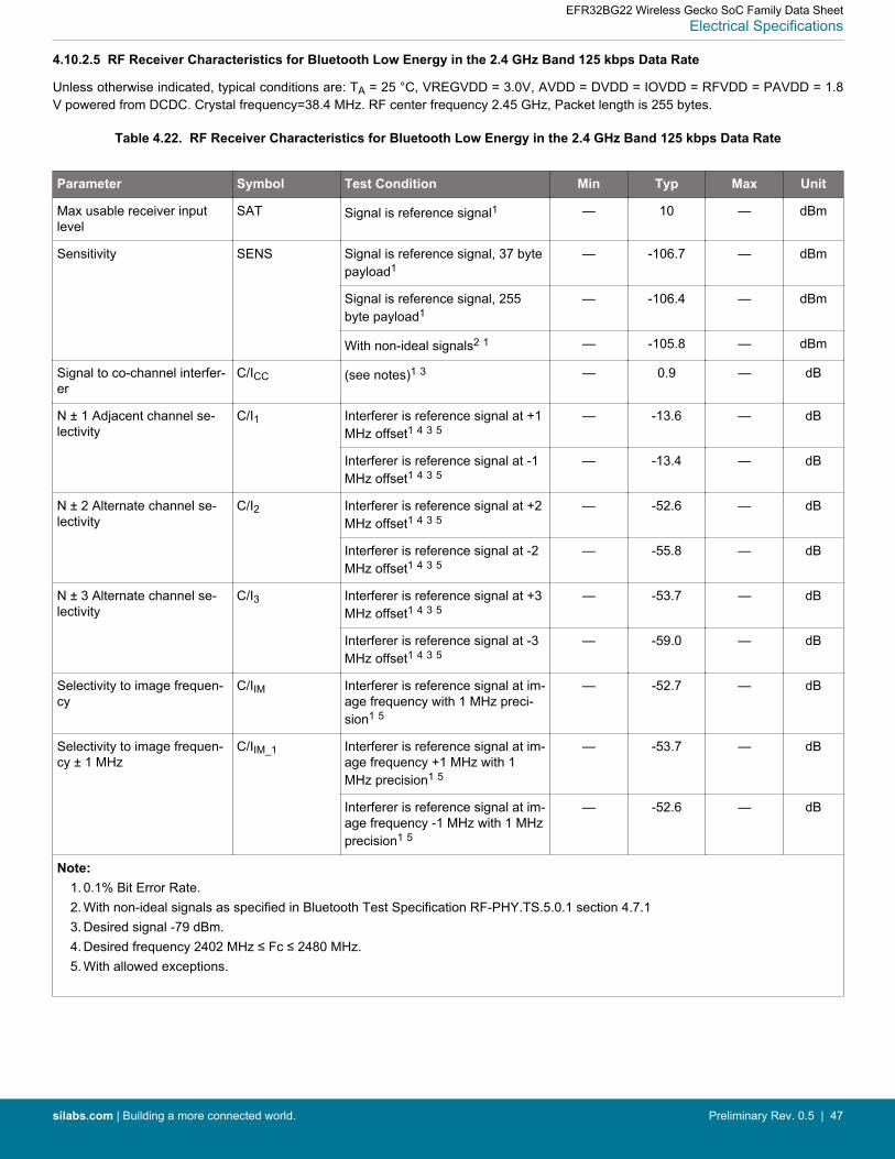
4.10.2.5 RF Receiver Characteristics for Bluetooth Low Energy in the 2.4 GHz Band 125 kbps Data Rate
Unless otherwise indicated, typical conditions are: TA = 25 °C, VREGVDD = 3.0V, AVDD = DVDD = IOVDD = RFVDD = PAVDD = 1.8V powered from DCDC. Crystal frequency=38.4 MHz. RF center frequency 2.45 GHz, Packet length is 255 bytes.
Table 4.22. RF Receiver Characteristics for Bluetooth Low Energy in the 2.4 GHz Band 125 kbps Data Rate
Parameter Symbol Test Condition Min Typ Max Unit
Max usable receiver inputlevel
SAT Signal is reference signal1 — 10 — dBm
Sensitivity SENS Signal is reference signal, 37 bytepayload1
— -106.7 — dBm
Signal is reference signal, 255byte payload1
— -106.4 — dBm
With non-ideal signals2 1 — -105.8 — dBm
Signal to co-channel interfer-er
C/ICC (see notes)1 3 — 0.9 — dB
N ± 1 Adjacent channel se-lectivity
C/I1 Interferer is reference signal at +1MHz offset1 4 3 5
— -13.6 — dB
Interferer is reference signal at -1MHz offset1 4 3 5
— -13.4 — dB
N ± 2 Alternate channel se-lectivity
C/I2 Interferer is reference signal at +2MHz offset1 4 3 5
— -52.6 — dB
Interferer is reference signal at -2MHz offset1 4 3 5
— -55.8 — dB
N ± 3 Alternate channel se-lectivity
C/I3 Interferer is reference signal at +3MHz offset1 4 3 5
— -53.7 — dB
Interferer is reference signal at -3MHz offset1 4 3 5
— -59.0 — dB
Selectivity to image frequen-cy
C/IIM Interferer is reference signal at im-age frequency with 1 MHz preci-sion1 5
— -52.7 — dB
Selectivity to image frequen-cy ± 1 MHz
C/IIM_1 Interferer is reference signal at im-age frequency +1 MHz with 1MHz precision1 5
— -53.7 — dB
Interferer is reference signal at im-age frequency -1 MHz with 1 MHzprecision1 5
— -52.6 — dB
Note:1. 0.1% Bit Error Rate.2. With non-ideal signals as specified in Bluetooth Test Specification RF-PHY.TS.5.0.1 section 4.7.13. Desired signal -79 dBm.4. Desired frequency 2402 MHz ≤ Fc ≤ 2480 MHz.5. With allowed exceptions.
EFR32BG22 Wireless Gecko SoC Family Data SheetElectrical Specifications
silabs.com | Building a more connected world. Preliminary Rev. 0.5 | 47
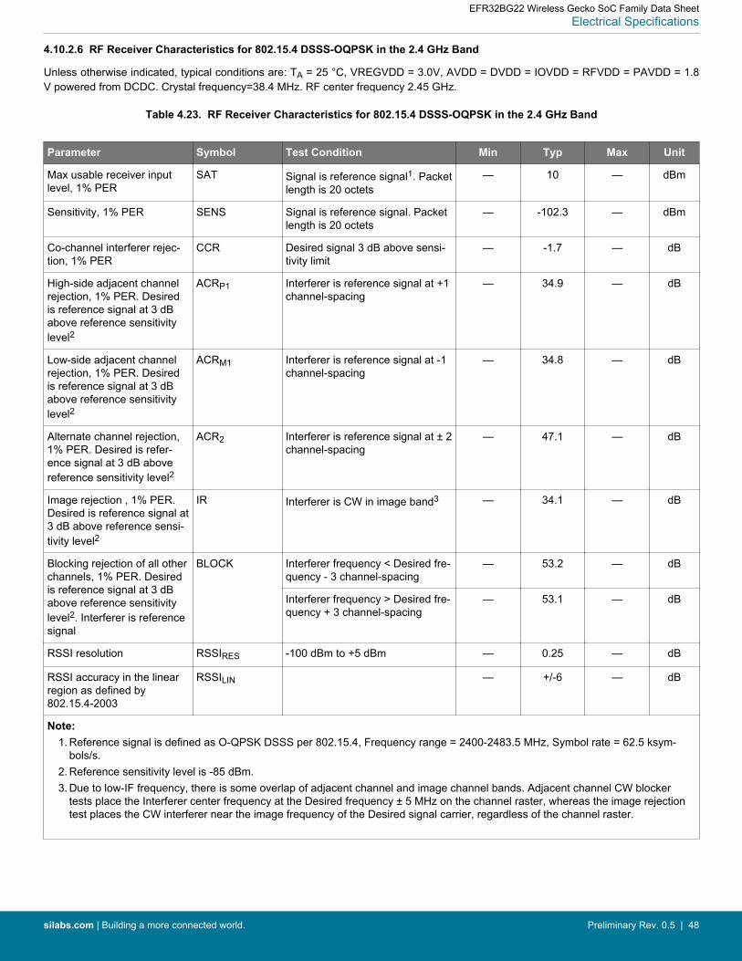
4.10.2.6 RF Receiver Characteristics for 802.15.4 DSSS-OQPSK in the 2.4 GHz Band
Unless otherwise indicated, typical conditions are: TA = 25 °C, VREGVDD = 3.0V, AVDD = DVDD = IOVDD = RFVDD = PAVDD = 1.8V powered from DCDC. Crystal frequency=38.4 MHz. RF center frequency 2.45 GHz.
Table 4.23. RF Receiver Characteristics for 802.15.4 DSSS-OQPSK in the 2.4 GHz Band
Parameter Symbol Test Condition Min Typ Max Unit
Max usable receiver inputlevel, 1% PER
SAT Signal is reference signal1. Packetlength is 20 octets
— 10 — dBm
Sensitivity, 1% PER SENS Signal is reference signal. Packetlength is 20 octets
— -102.3 — dBm
Co-channel interferer rejec-tion, 1% PER
CCR Desired signal 3 dB above sensi-tivity limit
— -1.7 — dB
High-side adjacent channelrejection, 1% PER. Desiredis reference signal at 3 dBabove reference sensitivitylevel2
ACRP1 Interferer is reference signal at +1channel-spacing
— 34.9 — dB
Low-side adjacent channelrejection, 1% PER. Desiredis reference signal at 3 dBabove reference sensitivitylevel2
ACRM1 Interferer is reference signal at -1channel-spacing
— 34.8 — dB
Alternate channel rejection,1% PER. Desired is refer-ence signal at 3 dB abovereference sensitivity level2
ACR2 Interferer is reference signal at ± 2channel-spacing
— 47.1 — dB
Image rejection , 1% PER.Desired is reference signal at3 dB above reference sensi-tivity level2
IR Interferer is CW in image band3 — 34.1 — dB
Blocking rejection of all otherchannels, 1% PER. Desiredis reference signal at 3 dBabove reference sensitivitylevel2. Interferer is referencesignal
BLOCK Interferer frequency < Desired fre-quency - 3 channel-spacing
— 53.2 — dB
Interferer frequency > Desired fre-quency + 3 channel-spacing
— 53.1 — dB
RSSI resolution RSSIRES -100 dBm to +5 dBm — 0.25 — dB
RSSI accuracy in the linearregion as defined by802.15.4-2003
RSSILIN — +/-6 — dB
Note:1. Reference signal is defined as O-QPSK DSSS per 802.15.4, Frequency range = 2400-2483.5 MHz, Symbol rate = 62.5 ksym-
bols/s.2. Reference sensitivity level is -85 dBm.3. Due to low-IF frequency, there is some overlap of adjacent channel and image channel bands. Adjacent channel CW blocker
tests place the Interferer center frequency at the Desired frequency ± 5 MHz on the channel raster, whereas the image rejectiontest places the CW interferer near the image frequency of the Desired signal carrier, regardless of the channel raster.
EFR32BG22 Wireless Gecko SoC Family Data SheetElectrical Specifications
silabs.com | Building a more connected world. Preliminary Rev. 0.5 | 48
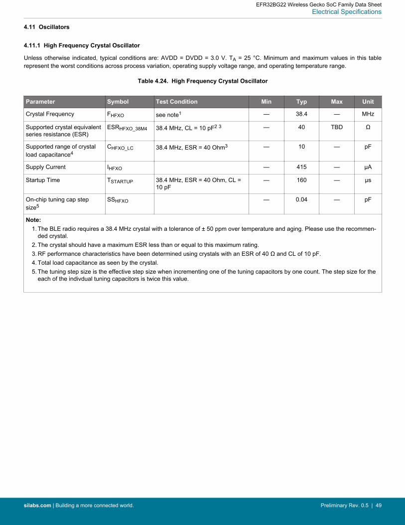
4.11 Oscillators
4.11.1 High Frequency Crystal Oscillator
Unless otherwise indicated, typical conditions are: AVDD = DVDD = 3.0 V. TA = 25 °C. Minimum and maximum values in this tablerepresent the worst conditions across process variation, operating supply voltage range, and operating temperature range.
Table 4.24. High Frequency Crystal Oscillator
Parameter Symbol Test Condition Min Typ Max Unit
Crystal Frequency FHFXO see note1 — 38.4 — MHz
Supported crystal equivalentseries resistance (ESR)
ESRHFXO_38M4 38.4 MHz, CL = 10 pF2 3 — 40 TBD Ω
Supported range of crystalload capacitance4
CHFXO_LC 38.4 MHz, ESR = 40 Ohm3 — 10 — pF
Supply Current IHFXO — 415 — µA
Startup Time TSTARTUP 38.4 MHz, ESR = 40 Ohm, CL =10 pF
— 160 — µs
On-chip tuning cap stepsize5
SSHFXO — 0.04 — pF
Note:1. The BLE radio requires a 38.4 MHz crystal with a tolerance of ± 50 ppm over temperature and aging. Please use the recommen-
ded crystal.2. The crystal should have a maximum ESR less than or equal to this maximum rating.3. RF performance characteristics have been determined using crystals with an ESR of 40 Ω and CL of 10 pF.4. Total load capacitance as seen by the crystal.5. The tuning step size is the effective step size when incrementing one of the tuning capacitors by one count. The step size for the
each of the indivdual tuning capacitors is twice this value.
EFR32BG22 Wireless Gecko SoC Family Data SheetElectrical Specifications
silabs.com | Building a more connected world. Preliminary Rev. 0.5 | 49
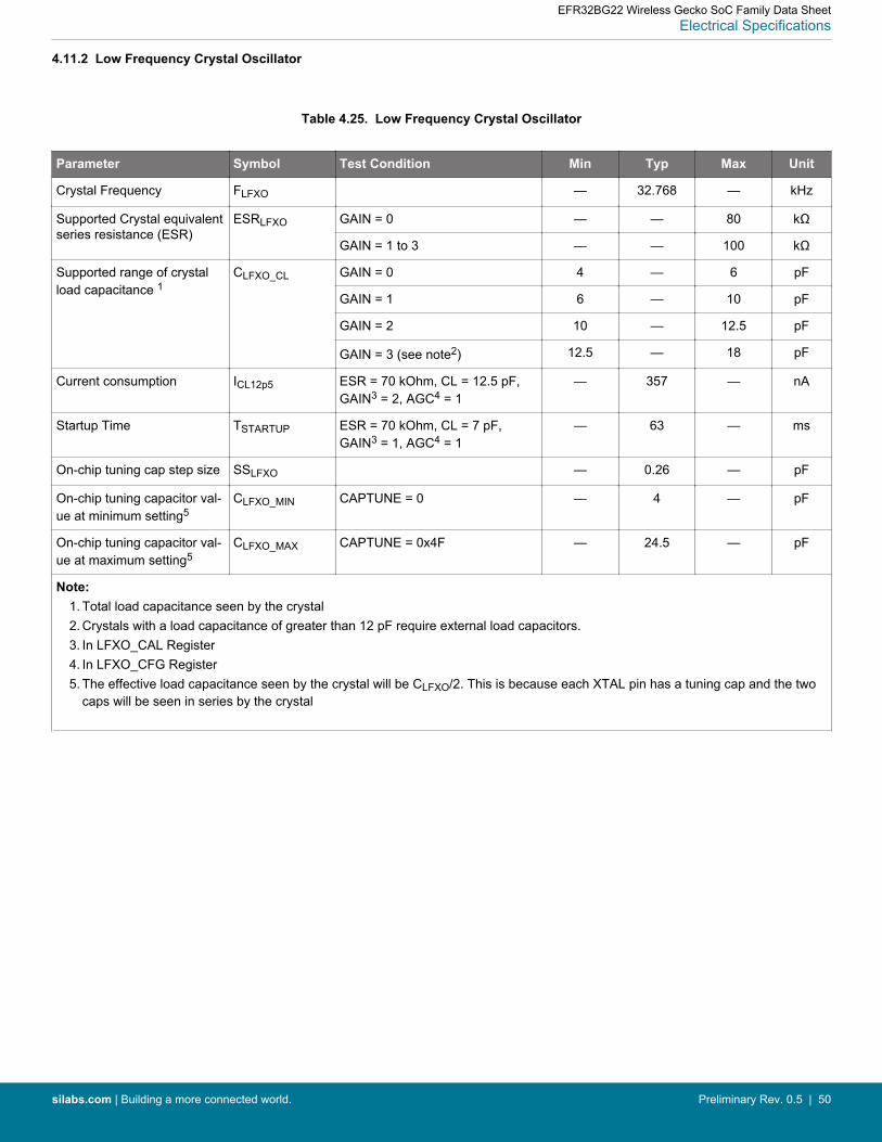
4.11.2 Low Frequency Crystal Oscillator
Table 4.25. Low Frequency Crystal Oscillator
Parameter Symbol Test Condition Min Typ Max Unit
Crystal Frequency FLFXO — 32.768 — kHz
Supported Crystal equivalentseries resistance (ESR)
ESRLFXO GAIN = 0 — — 80 kΩ
GAIN = 1 to 3 — — 100 kΩ
Supported range of crystalload capacitance 1
CLFXO_CL GAIN = 0 4 — 6 pF
GAIN = 1 6 — 10 pF
GAIN = 2 10 — 12.5 pF
GAIN = 3 (see note2) 12.5 — 18 pF
Current consumption ICL12p5 ESR = 70 kOhm, CL = 12.5 pF,GAIN3 = 2, AGC4 = 1
— 357 — nA
Startup Time TSTARTUP ESR = 70 kOhm, CL = 7 pF,GAIN3 = 1, AGC4 = 1
— 63 — ms
On-chip tuning cap step size SSLFXO — 0.26 — pF
On-chip tuning capacitor val-ue at minimum setting5
CLFXO_MIN CAPTUNE = 0 — 4 — pF
On-chip tuning capacitor val-ue at maximum setting5
CLFXO_MAX CAPTUNE = 0x4F — 24.5 — pF
Note:1. Total load capacitance seen by the crystal2. Crystals with a load capacitance of greater than 12 pF require external load capacitors.3. In LFXO_CAL Register4. In LFXO_CFG Register5. The effective load capacitance seen by the crystal will be CLFXO/2. This is because each XTAL pin has a tuning cap and the two
caps will be seen in series by the crystal
EFR32BG22 Wireless Gecko SoC Family Data SheetElectrical Specifications
silabs.com | Building a more connected world. Preliminary Rev. 0.5 | 50
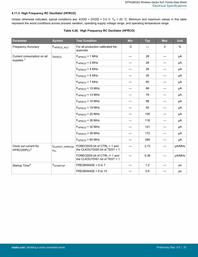
4.11.3 High Frequency RC Oscillator (HFRCO)
Unless otherwise indicated, typical conditions are: AVDD = DVDD = 3.0 V. TA = 25 °C. Minimum and maximum values in this tablerepresent the worst conditions across process variation, operating supply voltage range, and operating temperature range.
Table 4.26. High Frequency RC Oscillator (HFRCO)
Parameter Symbol Test Condition Min Typ Max Unit
Frequency Accuracy FHFRCO_ACC For all production calibrated fre-quencies
-3 — 3 %
Current consumption on allsupplies 1
IHFRCO FHFRCO = 1 MHz — 28 — µA
FHFRCO = 2 MHz — 28 — µA
FHFRCO = 4 MHz — 28 — µA
FHFRCO = 5 MHz — 30 — µA
FHFRCO = 7 MHz — 60 — µA
FHFRCO = 10 MHz — 66 — µA
FHFRCO = 13 MHz — 79 — µA
FHFRCO = 16 MHz — 88 — µA
FHFRCO = 19 MHz — 92 — µA
FHFRCO = 20 MHz — 105 — µA
FHFRCO = 26 MHz — 118 — µA
FHFRCO = 32 MHz — 141 — µA
FHFRCO = 38 MHz — 172 — µA
FHFRCO = 80 MHz — 289 — µA
Clock out current forHFRCODPLL2
ICLKOUT_HFRCOD
PLL
FORECEEN bit of CTRL = 1 andthe CLKOUTDIS0 bit of TEST = 1.
— 2.72 — µA/MHz
FORECEEN bit of CTRL i= 1 andthe CLKOUTDIS1 bit of TEST = 1.
— 0.36 — µA/MHz
Startup Time3 TSTARTUP FREQRANGE = 0 to 7 — 1.2 — µs
FREQRANGE = 8 to 15 — 0.6 — µs
EFR32BG22 Wireless Gecko SoC Family Data SheetElectrical Specifications
silabs.com | Building a more connected world. Preliminary Rev. 0.5 | 51
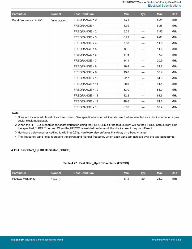
Parameter Symbol Test Condition Min Typ Max Unit
Band Frequency Limits4 fHFRCO_BAND FREQRANGE = 0 3.71 — 5.24 MHz
FREQRANGE = 1 4.39 — 6.26 MHz
FREQRANGE = 2 5.25 — 7.55 MHz
FREQRANGE = 3 6.22 — 9.01 MHz
FREQRANGE = 4 7.88 — 11.6 MHz
FREQRANGE = 5 9.9 — 14.6 MHz
FREQRANGE = 6 11.5 — 17.0 MHz
FREQRANGE = 7 14.1 — 20.9 MHz
FREQRANGE = 8 16.4 — 24.7 MHz
FREQRANGE = 9 19.8 — 30.4 MHz
FREQRANGE = 10 22.7 — 34.9 MHz
FREQRANGE = 11 28.6 — 44.4 MHz
FREQRANGE = 12 33.0 — 51.0 MHz
FREQRANGE = 13 42.2 — 64.6 MHz
FREQRANGE = 14 48.8 — 74.8 MHz
FREQRANGE = 15 57.6 — 87.4 MHz
Note:1. Does not include additional clock tree current. See specifications for additional current when selected as a clock source for a par-
ticular clock multiplexer.2. When the HFRCO is enabled for characterization using the FORCEEN bit, the total current will be the HFRCO core current plus
the specified CLKOUT current. When the HFRCO is enabled on demand, the clock current may be different.3. Hardware delay ensures settling to within ± 0.5%. Hardware also enforces this delay on a band change.4. The frequency band limits represent the lowest and highest freqeuncy which each band can achieve over the operating range.
4.11.4 Fast Start_Up RC Oscillator (FSRCO)
Table 4.27. Fast Start_Up RC Oscillator (FSRCO)
Parameter Symbol Test Condition Min Typ Max Unit
FSRCO frequency FFSRCO 17.2 20 21.2 MHz
EFR32BG22 Wireless Gecko SoC Family Data SheetElectrical Specifications
silabs.com | Building a more connected world. Preliminary Rev. 0.5 | 52
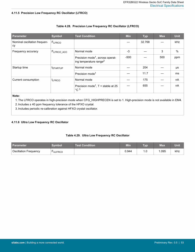
4.11.5 Precision Low Frequency RC Oscillator (LFRCO)
Table 4.28. Precision Low Frequency RC Oscillator (LFRCO)
Parameter Symbol Test Condition Min Typ Max Unit
Nominal oscillation frequen-cy
FLFRCO — 32.768 — kHz
Frequency accuracy FLFRCO_ACC Normal mode -3 — 3 %
Precision mode1, across operat-ing temperature range2
-500 — 500 ppm
Startup time tSTARTUP Normal mode — 204 — µs
Precision mode1 — 11.7 — ms
Current consumption ILFRCO Normal mode — 175 — nA
Precision mode1, T = stable at 25°C 3
— 655 — nA
Note:1. The LFRCO operates in high-precision mode when CFG_HIGHPRECEN is set to 1. High-precision mode is not available in EM4.2. Includes ± 40 ppm frequency tolerance of the HFXO crystal.3. Includes periodic re-calibration against HFXO crystal oscillator.
4.11.6 Ultra Low Frequency RC Oscillator
Table 4.29. Ultra Low Frequency RC Oscillator
Parameter Symbol Test Condition Min Typ Max Unit
Oscillation Frequency FULFRCO 0.944 1.0 1.095 kHz
EFR32BG22 Wireless Gecko SoC Family Data SheetElectrical Specifications
silabs.com | Building a more connected world. Preliminary Rev. 0.5 | 53
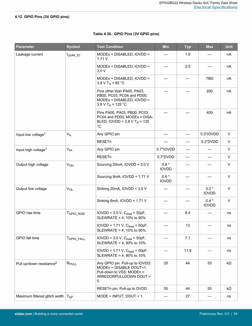
4.12 GPIO Pins (3V GPIO pins)
Table 4.30. GPIO Pins (3V GPIO pins)
Parameter Symbol Test Condition Min Typ Max Unit
Leakage current ILEAK_IO MODEx = DISABLED, IOVDD =1.71 V
— 1.9 — nA
MODEx = DISABLED, IOVDD =3.0 V
— 2.5 — nA
MODEx = DISABLED, IOVDD =3.8 V TA = 85 °C
— — TBD nA
Pins other than PA00, PA03,PB00, PC03, PC04 and PD00;MODEx = DISABLED, IOVDD =3.8 V TA = 125 °C
— — 200 nA
Pins PA00, PA03, PB00, PC03,PC04 and PD00; MODEx = DISA-BLED, IOVDD = 3.8 V TA = 125°C
— — 400 nA
Input low voltage1 VIL Any GPIO pin — — 0.3*IOVDD V
RESETn — — 0.3*DVDD V
Input high voltage1 VIH Any GPIO pin 0.7*IOVDD — — V
RESETn 0.7*DVDD — — V
Output high voltage VOH Sourcing 20mA, IOVDD = 3.0 V 0.8 *IOVDD
— — V
Sourcing 8mA, IOVDD = 1.71 V 0.6 *IOVDD
— — V
Output low voltage VOL Sinking 20mA, IOVDD = 3.0 V — — 0.2 *IOVDD
V
Sinking 8mA, IOVDD = 1.71 V — — 0.4 *IOVDD
V
GPIO rise time TGPIO_RISE IOVDD = 3.0 V, Cload = 50pF,SLEWRATE = 4, 10% to 90%
— 8.4 — ns
IOVDD = 1.71 V, Cload = 50pF,SLEWRATE = 4, 10% to 90%
— 13 — ns
GPIO fall time TGPIO_FALL IOVDD = 3.0 V, Cload = 50pF,SLEWRATE = 4, 90% to 10%
— 7.1 — ns
IOVDD = 1.71 V, Cload = 50pF,SLEWRATE = 4, 90% to 10%
— 11.9 — ns
Pull up/down resistance2 RPULL Any GPIO pin. Pull-up to IOVDD:MODEn = DISABLE DOUT=1.Pull-down to VSS: MODEn =WIREDORPULLDOWN DOUT =0.
35 44 55 kΩ
RESETn pin. Pull-up to DVDD 35 44 55 kΩ
Maximum filtered glitch width TGF MODE = INPUT, DOUT = 1 — 27 — ns
EFR32BG22 Wireless Gecko SoC Family Data SheetElectrical Specifications
silabs.com | Building a more connected world. Preliminary Rev. 0.5 | 54
Parameter Symbol Test Condition Min Typ Max Unit
Note:1. GPIO input thresholds are proportional to the IOVDD pin. RESETn input thresholds are proportional to DVDD.2. GPIO pull-ups connect to IOVDD supply, pull-downs connect to VSS. RESETn pull-up connects to DVDD.
EFR32BG22 Wireless Gecko SoC Family Data SheetElectrical Specifications
silabs.com | Building a more connected world. Preliminary Rev. 0.5 | 55
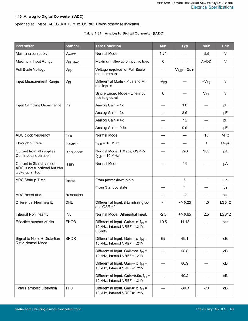
4.13 Analog to Digital Converter (IADC)
Specified at 1 Msps, ADCCLK = 10 MHz, OSR=2, unless otherwise indicated.
Table 4.31. Analog to Digital Converter (IADC)
Parameter Symbol Test Condition Min Typ Max Unit
Main analog supply VAVDD Normal Mode 1.71 — 3.8 V
Maximum Input Range VIN_MAX Maximum allowable input voltage 0 — AVDD V
Full-Scale Voltage VFS Voltage required for Full-Scalemeasurement
— VREF / Gain —
Input Measurement Range VIN Differential Mode - Plus and Mi-nus inputs
-VFS — +VFS V
Single Ended Mode - One inputtied to ground
0 — VFS V
Input Sampling Capacitance Cs Analog Gain = 1x — 1.8 — pF
Analog Gain = 2x — 3.6 — pF
Analog Gain = 4x — 7.2 — pF
Analog Gain = 0.5x — 0.9 — pF
ADC clock frequency fCLK Normal Mode — — 10 MHz
Throughput rate fSAMPLE fCLK = 10 MHz — — 1 Msps
Current from all supplies,Continuous operation
IADC_CONT Normal Mode, 1 Msps, OSR=2,fCLK = 10 MHz
— 290 385 µA
Current in Standby mode.ADC is not functional but canwake up in 1us.
ISTBY Normal Mode — 16 — µA
ADC Startup Time tstartup From power down state — 5 — µs
From Standby state — 1 — µs
ADC Resolution Resolution — 12 — bits
Differential Nonlinearity DNL Differential Input. (No missing co-des OSR =2
-1 +/- 0.25 1.5 LSB12
Integral Nonlinearity INL Normal Mode. Differential Input. -2.5 +/- 0.65 2.5 LSB12
Effective number of bits ENOB Differential Input. Gain=1x, fIN =10 kHz, Internal VREF=1.21V.OSR=2
10.5 11.18 — bits
Signal to Noise + DistortionRatio Normal Mode
SNDR Differential Input. Gain=1x, fIN =10 kHz, Internal VREF=1.21V
65 69.1 — dB
Differential Input. Gain=2x, fIN =10 kHz, Internal VREF=1.21V
— 68.8 — dB
Differential Input. Gain=4x, fIN =10 kHz, Internal VREF=1.21V
— 66.9 — dB
Differential Input. Gain=0.5x, fIN =10 kHz, Internal VREF=1.21V
— 69.2 — dB
Total Harmonic Distortion THD Differential Input. Gain=1x, fIN =10 kHz, Internal VREF=1.21V
— -80.3 -70 dB
EFR32BG22 Wireless Gecko SoC Family Data SheetElectrical Specifications
silabs.com | Building a more connected world. Preliminary Rev. 0.5 | 56
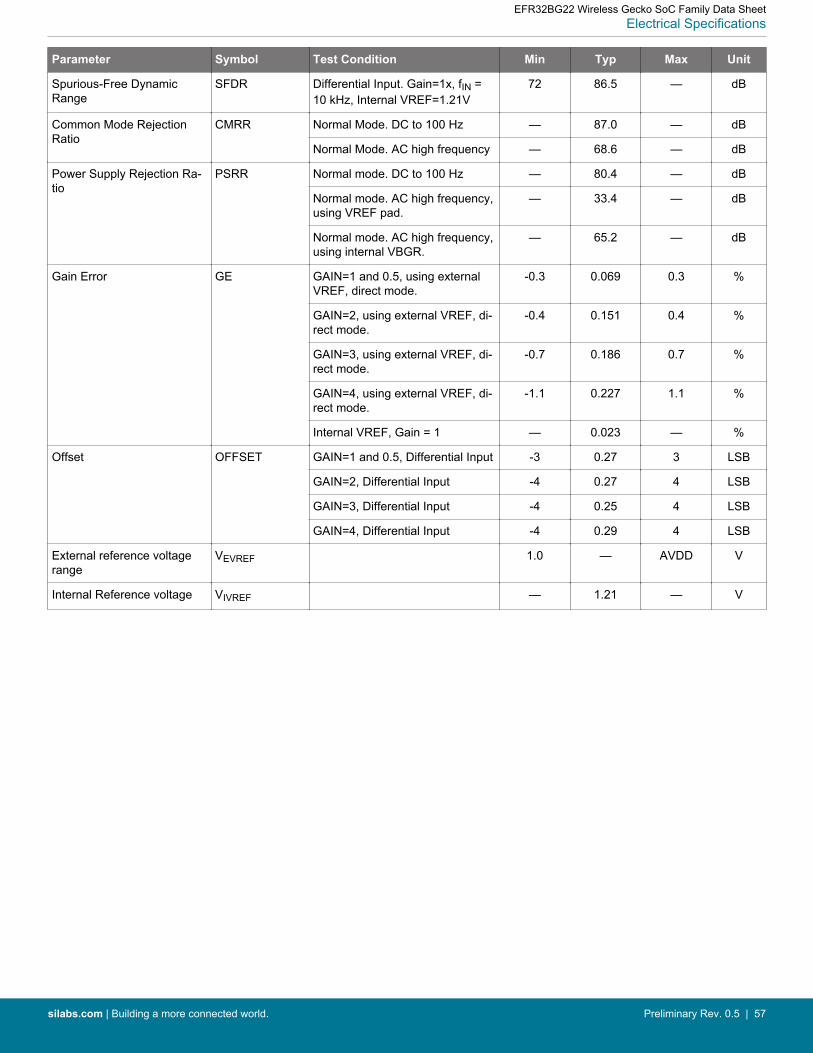
Parameter Symbol Test Condition Min Typ Max Unit
Spurious-Free DynamicRange
SFDR Differential Input. Gain=1x, fIN =10 kHz, Internal VREF=1.21V
72 86.5 — dB
Common Mode RejectionRatio
CMRR Normal Mode. DC to 100 Hz — 87.0 — dB
Normal Mode. AC high frequency — 68.6 — dB
Power Supply Rejection Ra-tio
PSRR Normal mode. DC to 100 Hz — 80.4 — dB
Normal mode. AC high frequency,using VREF pad.
— 33.4 — dB
Normal mode. AC high frequency,using internal VBGR.
— 65.2 — dB
Gain Error GE GAIN=1 and 0.5, using externalVREF, direct mode.
-0.3 0.069 0.3 %
GAIN=2, using external VREF, di-rect mode.
-0.4 0.151 0.4 %
GAIN=3, using external VREF, di-rect mode.
-0.7 0.186 0.7 %
GAIN=4, using external VREF, di-rect mode.
-1.1 0.227 1.1 %
Internal VREF, Gain = 1 — 0.023 — %
Offset OFFSET GAIN=1 and 0.5, Differential Input -3 0.27 3 LSB
GAIN=2, Differential Input -4 0.27 4 LSB
GAIN=3, Differential Input -4 0.25 4 LSB
GAIN=4, Differential Input -4 0.29 4 LSB
External reference voltagerange
VEVREF 1.0 — AVDD V
Internal Reference voltage VIVREF — 1.21 — V
EFR32BG22 Wireless Gecko SoC Family Data SheetElectrical Specifications
silabs.com | Building a more connected world. Preliminary Rev. 0.5 | 57
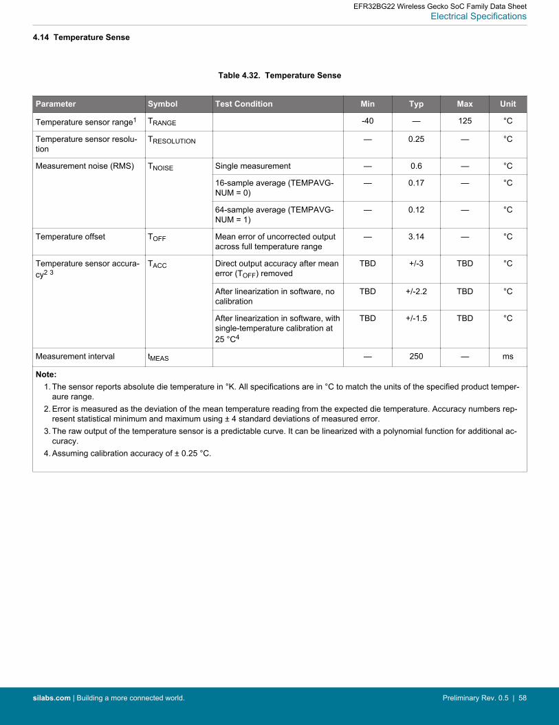
4.14 Temperature Sense
Table 4.32. Temperature Sense
Parameter Symbol Test Condition Min Typ Max Unit
Temperature sensor range1 TRANGE -40 — 125 °C
Temperature sensor resolu-tion
TRESOLUTION — 0.25 — °C
Measurement noise (RMS) TNOISE Single measurement — 0.6 — °C
16-sample average (TEMPAVG-NUM = 0)
— 0.17 — °C
64-sample average (TEMPAVG-NUM = 1)
— 0.12 — °C
Temperature offset TOFF Mean error of uncorrected outputacross full temperature range
— 3.14 — °C
Temperature sensor accura-cy2 3
TACC Direct output accuracy after meanerror (TOFF) removed
TBD +/-3 TBD °C
After linearization in software, nocalibration
TBD +/-2.2 TBD °C
After linearization in software, withsingle-temperature calibration at25 °C4
TBD +/-1.5 TBD °C
Measurement interval tMEAS — 250 — ms
Note:1. The sensor reports absolute die temperature in °K. All specifications are in °C to match the units of the specified product temper-
aure range.2. Error is measured as the deviation of the mean temperature reading from the expected die temperature. Accuracy numbers rep-
resent statistical minimum and maximum using ± 4 standard deviations of measured error.3. The raw output of the temperature sensor is a predictable curve. It can be linearized with a polynomial function for additional ac-
curacy.4. Assuming calibration accuracy of ± 0.25 °C.
EFR32BG22 Wireless Gecko SoC Family Data SheetElectrical Specifications
silabs.com | Building a more connected world. Preliminary Rev. 0.5 | 58
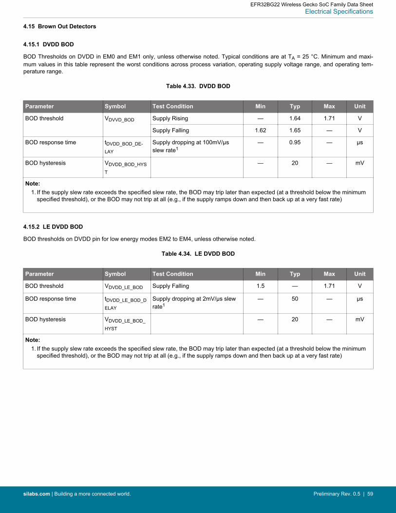
4.15 Brown Out Detectors
4.15.1 DVDD BOD
BOD Thresholds on DVDD in EM0 and EM1 only, unless otherwise noted. Typical conditions are at TA = 25 °C. Minimum and maxi-mum values in this table represent the worst conditions across process variation, operating supply voltage range, and operating tem-perature range.
Table 4.33. DVDD BOD
Parameter Symbol Test Condition Min Typ Max Unit
BOD threshold VDVVD_BOD Supply Rising — 1.64 1.71 V
Supply Falling 1.62 1.65 — V
BOD response time tDVDD_BOD_DE-
LAY
Supply dropping at 100mV/µsslew rate1
— 0.95 — µs
BOD hysteresis VDVDD_BOD_HYS
T
— 20 — mV
Note:1. If the supply slew rate exceeds the specified slew rate, the BOD may trip later than expected (at a threshold below the minimum
specified threshold), or the BOD may not trip at all (e.g., if the supply ramps down and then back up at a very fast rate)
4.15.2 LE DVDD BOD
BOD thresholds on DVDD pin for low energy modes EM2 to EM4, unless otherwise noted.
Table 4.34. LE DVDD BOD
Parameter Symbol Test Condition Min Typ Max Unit
BOD threshold VDVDD_LE_BOD Supply Falling 1.5 — 1.71 V
BOD response time tDVDD_LE_BOD_D
ELAY
Supply dropping at 2mV/µs slewrate1
— 50 — µs
BOD hysteresis VDVDD_LE_BOD_
HYST
— 20 — mV
Note:1. If the supply slew rate exceeds the specified slew rate, the BOD may trip later than expected (at a threshold below the minimum
specified threshold), or the BOD may not trip at all (e.g., if the supply ramps down and then back up at a very fast rate)
EFR32BG22 Wireless Gecko SoC Family Data SheetElectrical Specifications
silabs.com | Building a more connected world. Preliminary Rev. 0.5 | 59
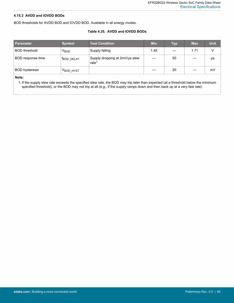
4.15.3 AVDD and IOVDD BODs
BOD thresholds for AVDD BOD and IOVDD BOD. Available in all energy modes.
Table 4.35. AVDD and IOVDD BODs
Parameter Symbol Test Condition Min Typ Max Unit
BOD threshold VBOD Supply falling 1.45 — 1.71 V
BOD response time tBOD_DELAY Supply dropping at 2mV/µs slewrate1
— 50 — µs
BOD hysteresis VBOD_HYST — 20 — mV
Note:1. If the supply slew rate exceeds the specified slew rate, the BOD may trip later than expected (at a threshold below the minimum
specified threshold), or the BOD may not trip at all (e.g., if the supply ramps down and then back up at a very fast rate)
EFR32BG22 Wireless Gecko SoC Family Data SheetElectrical Specifications
silabs.com | Building a more connected world. Preliminary Rev. 0.5 | 60
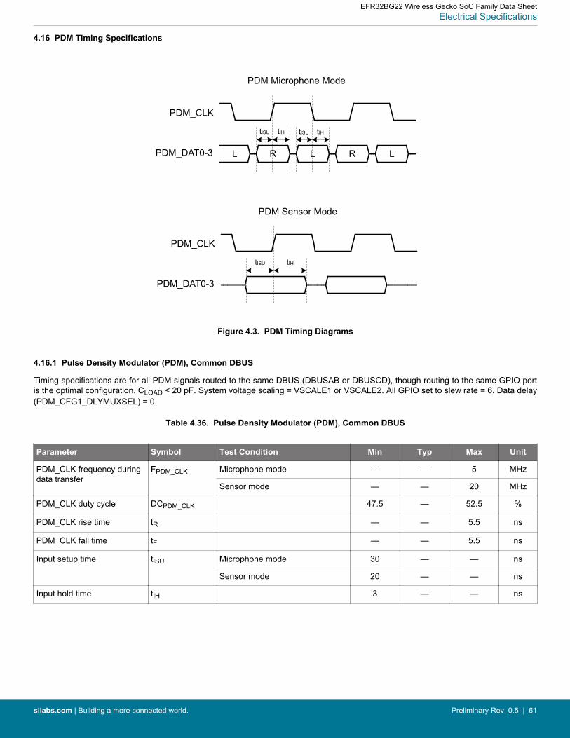
4.16 PDM Timing Specifications
L R L R L
tIHtISU
PDM Microphone Mode
PDM_CLK
PDM_DAT0-3
tIHtISU
PDM Sensor Mode
PDM_CLK
PDM_DAT0-3
tIHtISU
Figure 4.3. PDM Timing Diagrams
4.16.1 Pulse Density Modulator (PDM), Common DBUS
Timing specifications are for all PDM signals routed to the same DBUS (DBUSAB or DBUSCD), though routing to the same GPIO portis the optimal configuration. CLOAD < 20 pF. System voltage scaling = VSCALE1 or VSCALE2. All GPIO set to slew rate = 6. Data delay(PDM_CFG1_DLYMUXSEL) = 0.
Table 4.36. Pulse Density Modulator (PDM), Common DBUS
Parameter Symbol Test Condition Min Typ Max Unit
PDM_CLK frequency duringdata transfer
FPDM_CLK Microphone mode — — 5 MHz
Sensor mode — — 20 MHz
PDM_CLK duty cycle DCPDM_CLK 47.5 — 52.5 %
PDM_CLK rise time tR — — 5.5 ns
PDM_CLK fall time tF — — 5.5 ns
Input setup time tISU Microphone mode 30 — — ns
Sensor mode 20 — — ns
Input hold time tIH 3 — — ns
EFR32BG22 Wireless Gecko SoC Family Data SheetElectrical Specifications
silabs.com | Building a more connected world. Preliminary Rev. 0.5 | 61
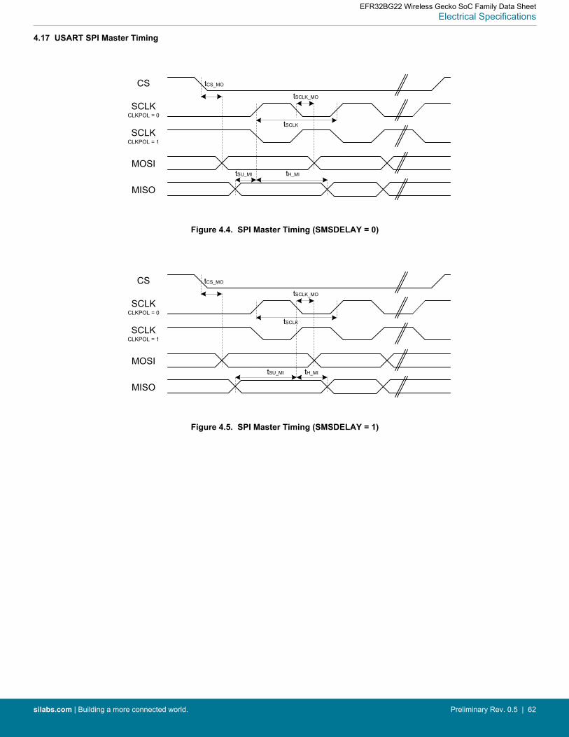
4.17 USART SPI Master Timing
CS
SCLKCLKPOL = 0
MOSI
MISO
tCS_MO
tH_MItSU_MI
tSCLK_MO
tSCLK
SCLKCLKPOL = 1
Figure 4.4. SPI Master Timing (SMSDELAY = 0)
CS
SCLKCLKPOL = 0
MOSI
MISO
tH_MItSU_MI
tSCLK_MO
tSCLK
SCLKCLKPOL = 1
tCS_MO
Figure 4.5. SPI Master Timing (SMSDELAY = 1)
EFR32BG22 Wireless Gecko SoC Family Data SheetElectrical Specifications
silabs.com | Building a more connected world. Preliminary Rev. 0.5 | 62
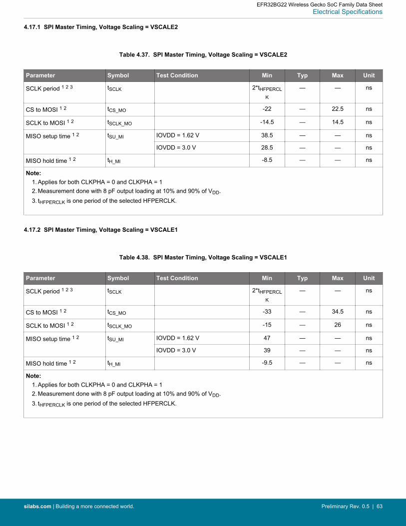
4.17.1 SPI Master Timing, Voltage Scaling = VSCALE2
Table 4.37. SPI Master Timing, Voltage Scaling = VSCALE2
Parameter Symbol Test Condition Min Typ Max Unit
SCLK period 1 2 3 tSCLK 2*tHFPERCL
K
— — ns
CS to MOSI 1 2 tCS_MO -22 — 22.5 ns
SCLK to MOSI 1 2 tSCLK_MO -14.5 — 14.5 ns
MISO setup time 1 2 tSU_MI IOVDD = 1.62 V 38.5 — — ns
IOVDD = 3.0 V 28.5 — — ns
MISO hold time 1 2 tH_MI -8.5 — — ns
Note:1. Applies for both CLKPHA = 0 and CLKPHA = 12. Measurement done with 8 pF output loading at 10% and 90% of VDD.3. tHFPERCLK is one period of the selected HFPERCLK.
4.17.2 SPI Master Timing, Voltage Scaling = VSCALE1
Table 4.38. SPI Master Timing, Voltage Scaling = VSCALE1
Parameter Symbol Test Condition Min Typ Max Unit
SCLK period 1 2 3 tSCLK 2*tHFPERCL
K
— — ns
CS to MOSI 1 2 tCS_MO -33 — 34.5 ns
SCLK to MOSI 1 2 tSCLK_MO -15 — 26 ns
MISO setup time 1 2 tSU_MI IOVDD = 1.62 V 47 — — ns
IOVDD = 3.0 V 39 — — ns
MISO hold time 1 2 tH_MI -9.5 — — ns
Note:1. Applies for both CLKPHA = 0 and CLKPHA = 12. Measurement done with 8 pF output loading at 10% and 90% of VDD.3. tHFPERCLK is one period of the selected HFPERCLK.
EFR32BG22 Wireless Gecko SoC Family Data SheetElectrical Specifications
silabs.com | Building a more connected world. Preliminary Rev. 0.5 | 63
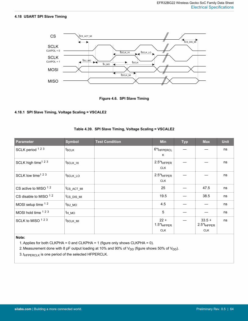
4.18 USART SPI Slave Timing
CS
SCLKCLKPOL = 0
MOSI
MISO
tCS_ACT_MI
tSCLK_HI
tSCLKtSU_MO
tH_MO
tSCLK_MI
tCS_DIS_MI
tSCLK_LO
SCLKCLKPOL = 1
Figure 4.6. SPI Slave Timing
4.18.1 SPI Slave Timing, Voltage Scaling = VSCALE2
Table 4.39. SPI Slave Timing, Voltage Scaling = VSCALE2
Parameter Symbol Test Condition Min Typ Max Unit
SCLK period 1 2 3 tSCLK 6*tHFPERCL
K
— — ns
SCLK high time1 2 3 tSCLK_HI 2.5*tHFPER
CLK
— — ns
SCLK low time1 2 3 tSCLK_LO 2.5*tHFPER
CLK
— — ns
CS active to MISO 1 2 tCS_ACT_MI 25 — 47.5 ns
CS disable to MISO 1 2 tCS_DIS_MI 19.5 — 38.5 ns
MOSI setup time 1 2 tSU_MO 4.5 — — ns
MOSI hold time 1 2 3 tH_MO 5 — — ns
SCLK to MISO 1 2 3 tSCLK_MI 22 +1.5*tHFPER
CLK
— 33.5 +2.5*tHFPER
CLK
ns
Note:1. Applies for both CLKPHA = 0 and CLKPHA = 1 (figure only shows CLKPHA = 0).2. Measurement done with 8 pF output loading at 10% and 90% of VDD (figure shows 50% of VDD).3. tHFPERCLK is one period of the selected HFPERCLK.
EFR32BG22 Wireless Gecko SoC Family Data SheetElectrical Specifications
silabs.com | Building a more connected world. Preliminary Rev. 0.5 | 64
4.18.2 SPI Slave Timing, Voltage Scaling = VSCALE1
Table 4.40. SPI Slave Timing, Voltage Scaling = VSCALE1
Parameter Symbol Test Condition Min Typ Max Unit
SCLK period 1 2 3 tSCLK 6*tHFPERCL
K
— — ns
SCLK high time1 2 3 tSCLK_HI 2.5*tHFPER
CLK
— — ns
SCLK low time1 2 3 tSCLK_LO 2.5*tHFPER
CLK
— — ns
CS active to MISO 1 2 tCS_ACT_MI 30.5 — 57.5 ns
CS disable to MISO 1 2 tCS_DIS_MI 25 — 55 ns
MOSI setup time 1 2 tSU_MO 7.5 — — ns
MOSI hold time 1 2 3 tH_MO 8.5 — — ns
SCLK to MISO 1 2 3 tSCLK_MI 24.5 +1.5*tHFPER
CLK
— 45.5 +2.5*tHFPER
CLK
ns
Note:1. Applies for both CLKPHA = 0 and CLKPHA = 1 (figure only shows CLKPHA = 0).2. Measurement done with 8 pF output loading at 10% and 90% of VDD (figure shows 50% of VDD).3. tHFPERCLK is one period of the selected HFPERCLK.
EFR32BG22 Wireless Gecko SoC Family Data SheetElectrical Specifications
silabs.com | Building a more connected world. Preliminary Rev. 0.5 | 65
4.19 I2C Electrical Specifications
4.19.1 I2C Standard-mode (Sm)
CLHR set to 0 in the I2Cn_CTRL register.
Table 4.41. I2C Standard-mode (Sm)
Parameter Symbol Test Condition Min Typ Max Unit
SCL clock frequency1 fSCL 0 — 100 kHz
SCL clock low time tLOW 4.7 — — µs
SCL clock high time tHIGH 4 — — µs
SDA set-up time tSU_DAT 250 — — ns
SDA hold time tHD_DAT 0 — — ns
Repeated START conditionset-up time
tSU_STA 4.7 — — µs
Repeated START conditionhold time
tHD_STA 4.0 — — µs
STOP condition set-up time tSU_STO 4.0 — — µs
Bus free time between aSTOP and START condition
tBUF 4.7 — — µs
Note:1. The maximum SCL clock frequency listed is assuming that an arbitrary clock frequency is available. The maximum attainable
SCL clock frequency may be slightly less using the HFXO or HFRCO due to the limited frequencies available. The CLKDIVshould be set to a value that keeps the SCL clock frequency below the max value listed.
EFR32BG22 Wireless Gecko SoC Family Data SheetElectrical Specifications
silabs.com | Building a more connected world. Preliminary Rev. 0.5 | 66
4.19.2 I2C Fast-mode (Fm)
CLHR set to 1 in the I2Cn_CTRL register.
Table 4.42. I2C Fast-mode (Fm)
Parameter Symbol Test Condition Min Typ Max Unit
SCL clock frequency1 fSCL 0 — 400 kHz
SCL clock low time tLOW 1.3 — — µs
SCL clock high time tHIGH 0.6 — — µs
SDA set-up time tSU_DAT 100 — — ns
SDA hold time tHD_DAT 0 — — ns
Repeated START conditionset-up time
tSU_STA 0.6 — — µs
Repeated START conditionhold time
tHD_STA 0.6 — — µs
STOP condition set-up time tSU_STO 0.6 — — µs
Bus free time between aSTOP and START condition
tBUF 1.3 — — µs
Note:1. The maximum SCL clock frequency listed is assuming that an arbitrary clock frequency is available. The maximum attainable
SCL clock frequency may be slightly less using the HFXO or HFRCO due to the limited frequencies available. The CLKDIVshould be set to a value that keeps the SCL clock frequency below the max value listed.
EFR32BG22 Wireless Gecko SoC Family Data SheetElectrical Specifications
silabs.com | Building a more connected world. Preliminary Rev. 0.5 | 67
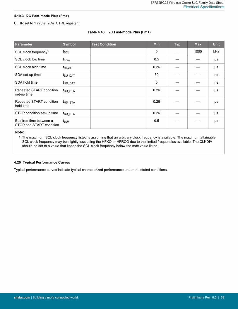
4.19.3 I2C Fast-mode Plus (Fm+)
CLHR set to 1 in the I2Cn_CTRL register.
Table 4.43. I2C Fast-mode Plus (Fm+)
Parameter Symbol Test Condition Min Typ Max Unit
SCL clock frequency1 fSCL 0 — 1000 kHz
SCL clock low time tLOW 0.5 — — µs
SCL clock high time tHIGH 0.26 — — µs
SDA set-up time tSU_DAT 50 — — ns
SDA hold time tHD_DAT 0 — — ns
Repeated START conditionset-up time
tSU_STA 0.26 — — µs
Repeated START conditionhold time
tHD_STA 0.26 — — µs
STOP condition set-up time tSU_STO 0.26 — — µs
Bus free time between aSTOP and START condition
tBUF 0.5 — — µs
Note:1. The maximum SCL clock frequency listed is assuming that an arbitrary clock frequency is available. The maximum attainable
SCL clock frequency may be slightly less using the HFXO or HFRCO due to the limited frequencies available. The CLKDIVshould be set to a value that keeps the SCL clock frequency below the max value listed.
4.20 Typical Performance Curves
Typical performance curves indicate typical characterized performance under the stated conditions.
EFR32BG22 Wireless Gecko SoC Family Data SheetElectrical Specifications
silabs.com | Building a more connected world. Preliminary Rev. 0.5 | 68
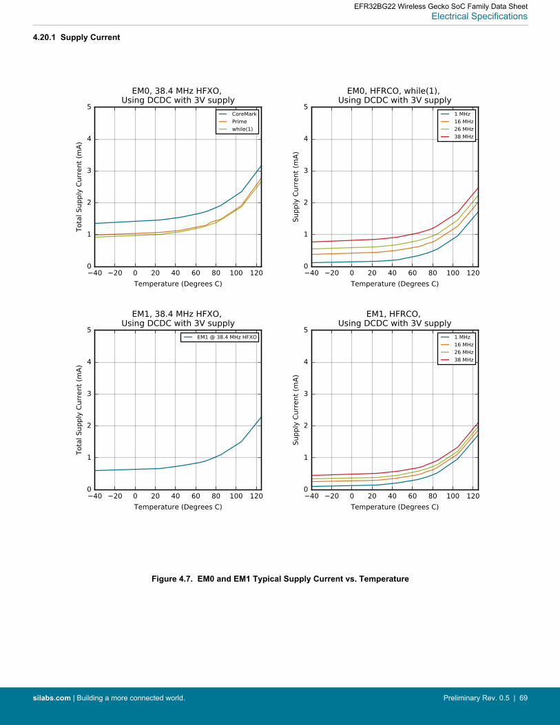
4.20.1 Supply Current
Figure 4.7. EM0 and EM1 Typical Supply Current vs. Temperature
EFR32BG22 Wireless Gecko SoC Family Data SheetElectrical Specifications
silabs.com | Building a more connected world. Preliminary Rev. 0.5 | 69
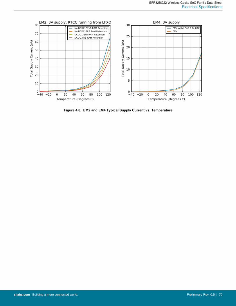
Figure 4.8. EM2 and EM4 Typical Supply Current vs. Temperature
EFR32BG22 Wireless Gecko SoC Family Data SheetElectrical Specifications
silabs.com | Building a more connected world. Preliminary Rev. 0.5 | 70
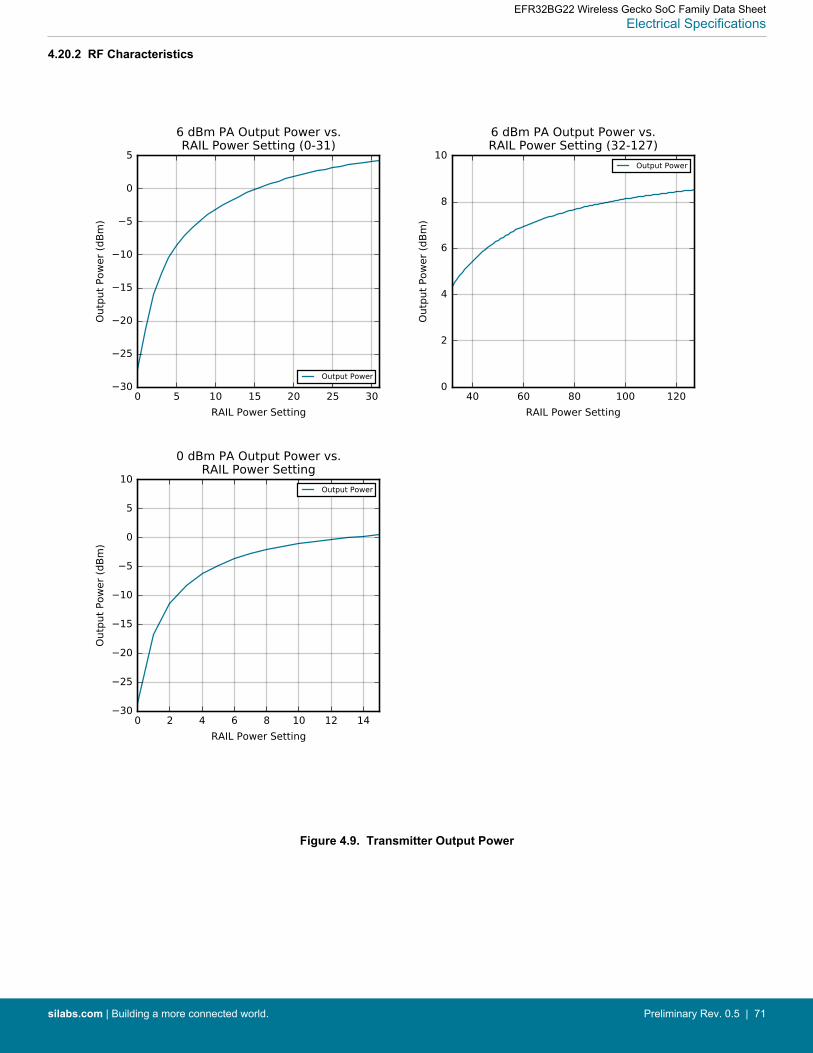
4.20.2 RF Characteristics
Figure 4.9. Transmitter Output Power
EFR32BG22 Wireless Gecko SoC Family Data SheetElectrical Specifications
silabs.com | Building a more connected world. Preliminary Rev. 0.5 | 71
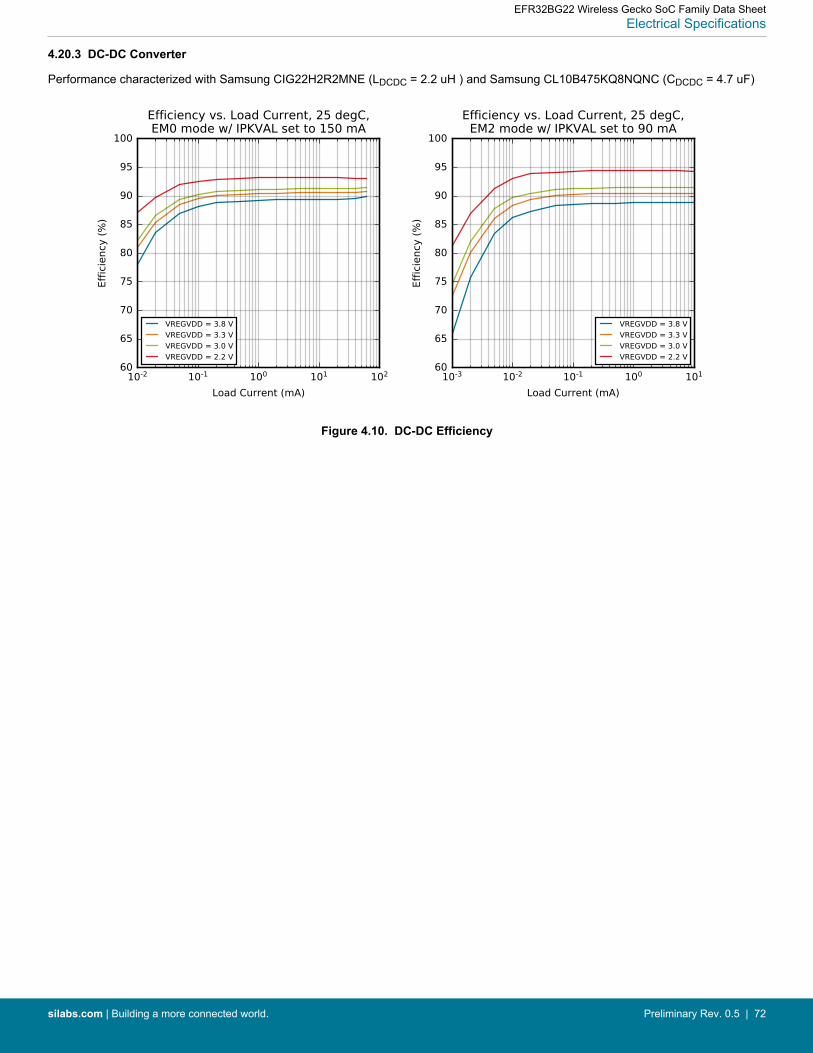
4.20.3 DC-DC Converter
Performance characterized with Samsung CIG22H2R2MNE (LDCDC = 2.2 uH ) and Samsung CL10B475KQ8NQNC (CDCDC = 4.7 uF)
Figure 4.10. DC-DC Efficiency
EFR32BG22 Wireless Gecko SoC Family Data SheetElectrical Specifications
silabs.com | Building a more connected world. Preliminary Rev. 0.5 | 72
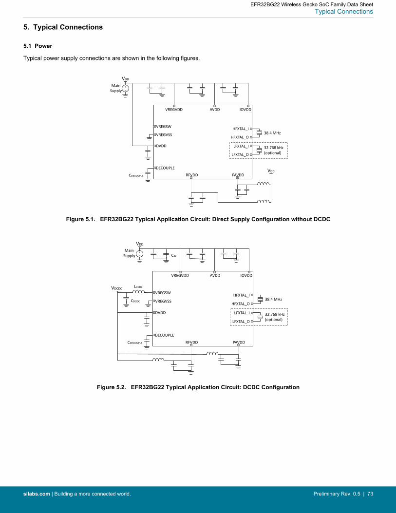
5. Typical Connections
5.1 Power
Typical power supply connections are shown in the following figures.
MainSupply
VDD
VREGVDD AVDD IOVDD
VREGSW
VREGVSS
DVDD
DECOUPLE
RFVDD PAVDD
HFXTAL_I
HFXTAL_O
LFXTAL_I
LFXTAL_O
+–
VDD
38.4 MHz
32.768 kHz(optional)
CDECOUPLE
Figure 5.1. EFR32BG22 Typical Application Circuit: Direct Supply Configuration without DCDC
MainSupply
VDCDC
VDD
VREGVDD AVDD IOVDD
VREGSW
VREGVSS
DVDD
DECOUPLE
RFVDD PAVDD
HFXTAL_I
HFXTAL_O
LFXTAL_I
LFXTAL_O
+–
LDCDC
CDCDC
CIN
CDECOUPLE
38.4 MHz
32.768 kHz(optional)
Figure 5.2. EFR32BG22 Typical Application Circuit: DCDC Configuration
EFR32BG22 Wireless Gecko SoC Family Data SheetTypical Connections
silabs.com | Building a more connected world. Preliminary Rev. 0.5 | 73
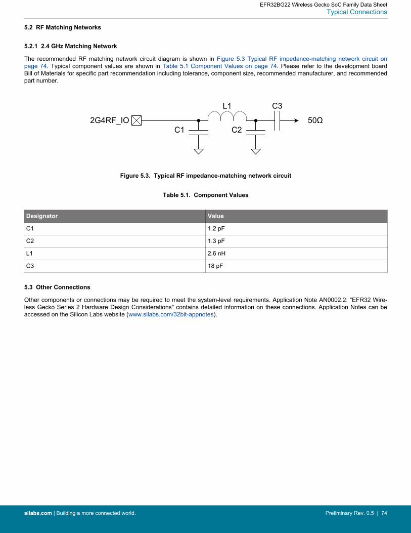
5.2 RF Matching Networks
5.2.1 2.4 GHz Matching Network
The recommended RF matching network circuit diagram is shown in Figure 5.3 Typical RF impedance-matching network circuit onpage 74. Typical component values are shown in Table 5.1 Component Values on page 74. Please refer to the development boardBill of Materials for specific part recommendation including tolerance, component size, recommended manufacturer, and recommendedpart number.
2G4RF_IO
L1
C1 C2
C3
50Ω
Figure 5.3. Typical RF impedance-matching network circuit
Table 5.1. Component Values
Designator Value
C1 1.2 pF
C2 1.3 pF
L1 2.6 nH
C3 18 pF
5.3 Other Connections
Other components or connections may be required to meet the system-level requirements. Application Note AN0002.2: "EFR32 Wire-less Gecko Series 2 Hardware Design Considerations" contains detailed information on these connections. Application Notes can beaccessed on the Silicon Labs website (www.silabs.com/32bit-appnotes).
EFR32BG22 Wireless Gecko SoC Family Data SheetTypical Connections
silabs.com | Building a more connected world. Preliminary Rev. 0.5 | 74
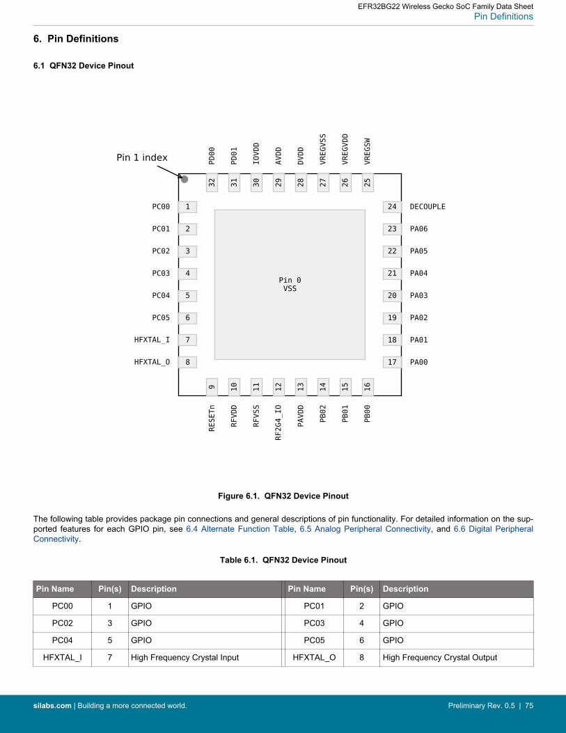
6. Pin Definitions
6.1 QFN32 Device Pinout
Figure 6.1. QFN32 Device Pinout
The following table provides package pin connections and general descriptions of pin functionality. For detailed information on the sup-ported features for each GPIO pin, see 6.4 Alternate Function Table, 6.5 Analog Peripheral Connectivity, and 6.6 Digital PeripheralConnectivity.
Table 6.1. QFN32 Device Pinout
Pin Name Pin(s) Description Pin Name Pin(s) Description
PC00 1 GPIO PC01 2 GPIO
PC02 3 GPIO PC03 4 GPIO
PC04 5 GPIO PC05 6 GPIO
HFXTAL_I 7 High Frequency Crystal Input HFXTAL_O 8 High Frequency Crystal Output
EFR32BG22 Wireless Gecko SoC Family Data SheetPin Definitions
silabs.com | Building a more connected world. Preliminary Rev. 0.5 | 75
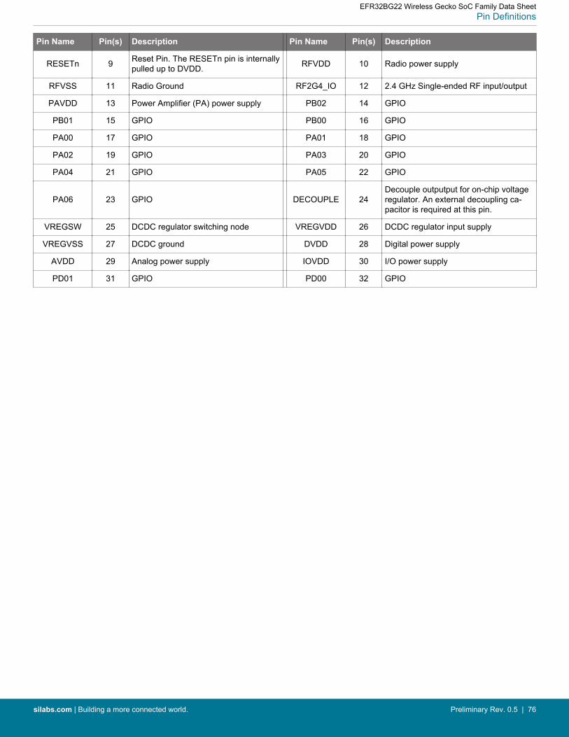
Pin Name Pin(s) Description Pin Name Pin(s) Description
RESETn 9 Reset Pin. The RESETn pin is internallypulled up to DVDD. RFVDD 10 Radio power supply
RFVSS 11 Radio Ground RF2G4_IO 12 2.4 GHz Single-ended RF input/output
PAVDD 13 Power Amplifier (PA) power supply PB02 14 GPIO
PB01 15 GPIO PB00 16 GPIO
PA00 17 GPIO PA01 18 GPIO
PA02 19 GPIO PA03 20 GPIO
PA04 21 GPIO PA05 22 GPIO
PA06 23 GPIO DECOUPLE 24Decouple outputput for on-chip voltageregulator. An external decoupling ca-pacitor is required at this pin.
VREGSW 25 DCDC regulator switching node VREGVDD 26 DCDC regulator input supply
VREGVSS 27 DCDC ground DVDD 28 Digital power supply
AVDD 29 Analog power supply IOVDD 30 I/O power supply
PD01 31 GPIO PD00 32 GPIO
EFR32BG22 Wireless Gecko SoC Family Data SheetPin Definitions
silabs.com | Building a more connected world. Preliminary Rev. 0.5 | 76
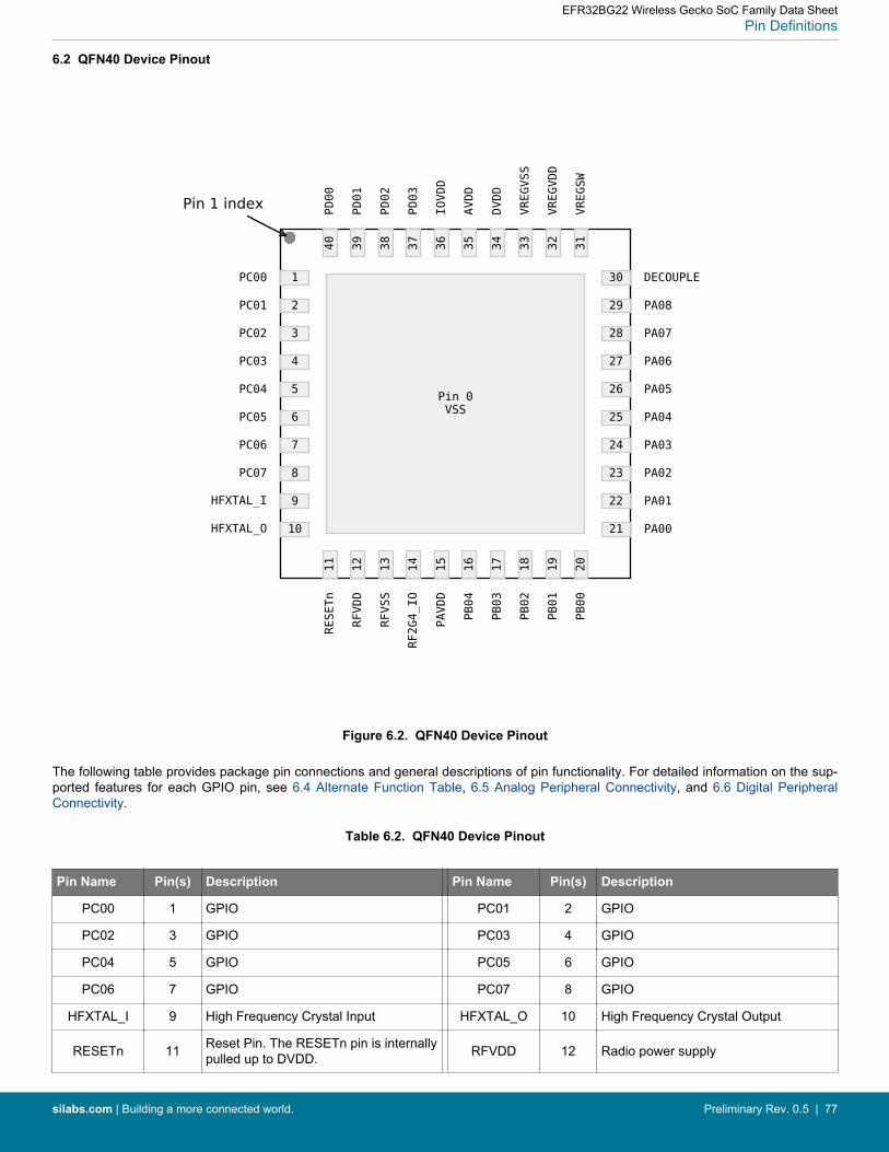
6.2 QFN40 Device Pinout
Figure 6.2. QFN40 Device Pinout
The following table provides package pin connections and general descriptions of pin functionality. For detailed information on the sup-ported features for each GPIO pin, see 6.4 Alternate Function Table, 6.5 Analog Peripheral Connectivity, and 6.6 Digital PeripheralConnectivity.
Table 6.2. QFN40 Device Pinout
Pin Name Pin(s) Description Pin Name Pin(s) Description
PC00 1 GPIO PC01 2 GPIO
PC02 3 GPIO PC03 4 GPIO
PC04 5 GPIO PC05 6 GPIO
PC06 7 GPIO PC07 8 GPIO
HFXTAL_I 9 High Frequency Crystal Input HFXTAL_O 10 High Frequency Crystal Output
RESETn 11 Reset Pin. The RESETn pin is internallypulled up to DVDD. RFVDD 12 Radio power supply
EFR32BG22 Wireless Gecko SoC Family Data SheetPin Definitions
silabs.com | Building a more connected world. Preliminary Rev. 0.5 | 77
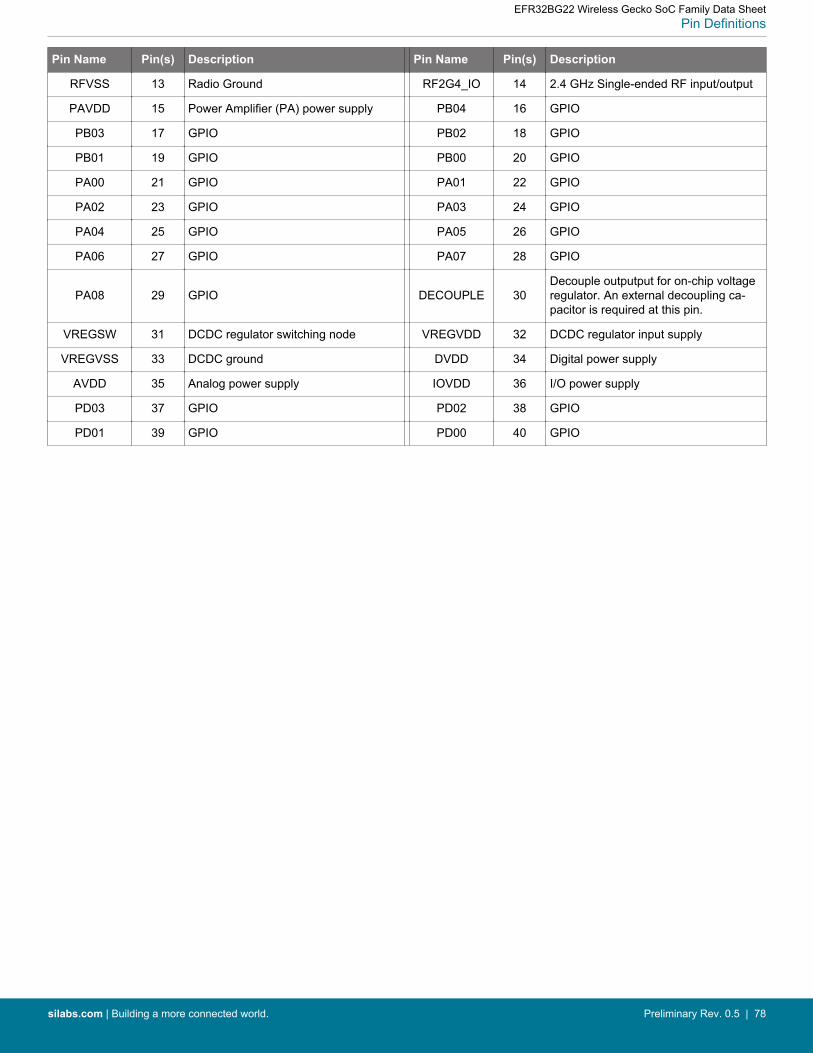
Pin Name Pin(s) Description Pin Name Pin(s) Description
RFVSS 13 Radio Ground RF2G4_IO 14 2.4 GHz Single-ended RF input/output
PAVDD 15 Power Amplifier (PA) power supply PB04 16 GPIO
PB03 17 GPIO PB02 18 GPIO
PB01 19 GPIO PB00 20 GPIO
PA00 21 GPIO PA01 22 GPIO
PA02 23 GPIO PA03 24 GPIO
PA04 25 GPIO PA05 26 GPIO
PA06 27 GPIO PA07 28 GPIO
PA08 29 GPIO DECOUPLE 30Decouple outputput for on-chip voltageregulator. An external decoupling ca-pacitor is required at this pin.
VREGSW 31 DCDC regulator switching node VREGVDD 32 DCDC regulator input supply
VREGVSS 33 DCDC ground DVDD 34 Digital power supply
AVDD 35 Analog power supply IOVDD 36 I/O power supply
PD03 37 GPIO PD02 38 GPIO
PD01 39 GPIO PD00 40 GPIO
EFR32BG22 Wireless Gecko SoC Family Data SheetPin Definitions
silabs.com | Building a more connected world. Preliminary Rev. 0.5 | 78
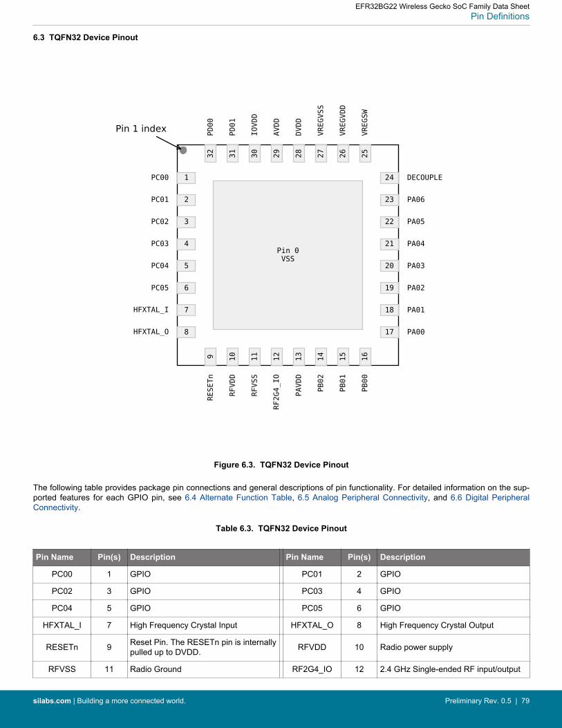
6.3 TQFN32 Device Pinout
Figure 6.3. TQFN32 Device Pinout
The following table provides package pin connections and general descriptions of pin functionality. For detailed information on the sup-ported features for each GPIO pin, see 6.4 Alternate Function Table, 6.5 Analog Peripheral Connectivity, and 6.6 Digital PeripheralConnectivity.
Table 6.3. TQFN32 Device Pinout
Pin Name Pin(s) Description Pin Name Pin(s) Description
PC00 1 GPIO PC01 2 GPIO
PC02 3 GPIO PC03 4 GPIO
PC04 5 GPIO PC05 6 GPIO
HFXTAL_I 7 High Frequency Crystal Input HFXTAL_O 8 High Frequency Crystal Output
RESETn 9 Reset Pin. The RESETn pin is internallypulled up to DVDD. RFVDD 10 Radio power supply
RFVSS 11 Radio Ground RF2G4_IO 12 2.4 GHz Single-ended RF input/output
EFR32BG22 Wireless Gecko SoC Family Data SheetPin Definitions
silabs.com | Building a more connected world. Preliminary Rev. 0.5 | 79
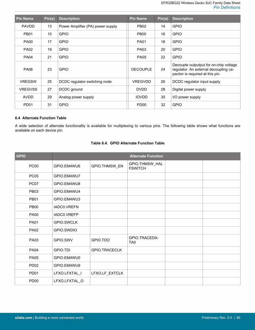
Pin Name Pin(s) Description Pin Name Pin(s) Description
PAVDD 13 Power Amplifier (PA) power supply PB02 14 GPIO
PB01 15 GPIO PB00 16 GPIO
PA00 17 GPIO PA01 18 GPIO
PA02 19 GPIO PA03 20 GPIO
PA04 21 GPIO PA05 22 GPIO
PA06 23 GPIO DECOUPLE 24Decouple outputput for on-chip voltageregulator. An external decoupling ca-pacitor is required at this pin.
VREGSW 25 DCDC regulator switching node VREGVDD 26 DCDC regulator input supply
VREGVSS 27 DCDC ground DVDD 28 Digital power supply
AVDD 29 Analog power supply IOVDD 30 I/O power supply
PD01 31 GPIO PD00 32 GPIO
6.4 Alternate Function Table
A wide selection of alternate functionality is available for multiplexing to various pins. The following table shows what functions areavailable on each device pin.
Table 6.4. GPIO Alternate Function Table
GPIO Alternate Function
PC00 GPIO.EM4WU6 GPIO.THMSW_EN GPIO.THMSW_HALFSWITCH
PC05 GPIO.EM4WU7
PC07 GPIO.EM4WU8
PB03 GPIO.EM4WU4
PB01 GPIO.EM4WU3
PB00 IADC0.VREFN
PA00 IADC0.VREFP
PA01 GPIO.SWCLK
PA02 GPIO.SWDIO
PA03 GPIO.SWV GPIO.TDO GPIO.TRACEDA-TA0
PA04 GPIO.TDI GPIO.TRACECLK
PA05 GPIO.EM4WU0
PD02 GPIO.EM4WU9
PD01 LFXO.LFXTAL_I LFXO.LF_EXTCLK
PD00 LFXO.LFXTAL_O
EFR32BG22 Wireless Gecko SoC Family Data SheetPin Definitions
silabs.com | Building a more connected world. Preliminary Rev. 0.5 | 80
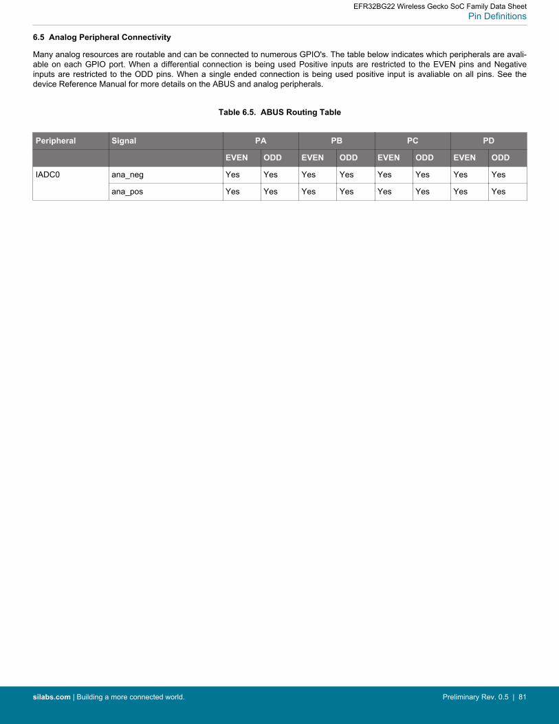
6.5 Analog Peripheral Connectivity
Many analog resources are routable and can be connected to numerous GPIO's. The table below indicates which peripherals are avali-able on each GPIO port. When a differential connection is being used Positive inputs are restricted to the EVEN pins and Negativeinputs are restricted to the ODD pins. When a single ended connection is being used positive input is avaliable on all pins. See thedevice Reference Manual for more details on the ABUS and analog peripherals.
Table 6.5. ABUS Routing Table
Peripheral Signal PA PB PC PD
EVEN ODD EVEN ODD EVEN ODD EVEN ODD
IADC0 ana_neg Yes Yes Yes Yes Yes Yes Yes Yes
ana_pos Yes Yes Yes Yes Yes Yes Yes Yes
EFR32BG22 Wireless Gecko SoC Family Data SheetPin Definitions
silabs.com | Building a more connected world. Preliminary Rev. 0.5 | 81
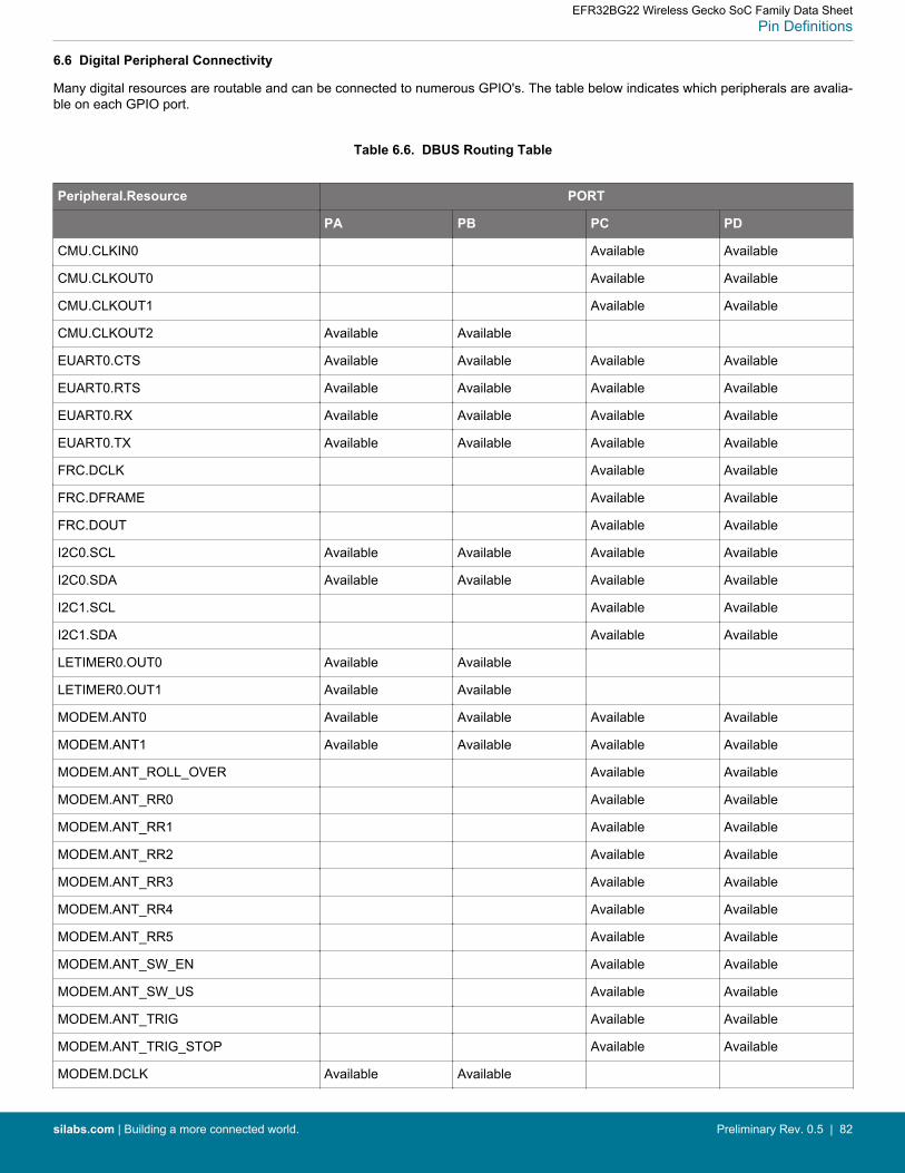
6.6 Digital Peripheral Connectivity
Many digital resources are routable and can be connected to numerous GPIO's. The table below indicates which peripherals are avalia-ble on each GPIO port.
Table 6.6. DBUS Routing Table
Peripheral.Resource PORT
PA PB PC PD
CMU.CLKIN0 Available Available
CMU.CLKOUT0 Available Available
CMU.CLKOUT1 Available Available
CMU.CLKOUT2 Available Available
EUART0.CTS Available Available Available Available
EUART0.RTS Available Available Available Available
EUART0.RX Available Available Available Available
EUART0.TX Available Available Available Available
FRC.DCLK Available Available
FRC.DFRAME Available Available
FRC.DOUT Available Available
I2C0.SCL Available Available Available Available
I2C0.SDA Available Available Available Available
I2C1.SCL Available Available
I2C1.SDA Available Available
LETIMER0.OUT0 Available Available
LETIMER0.OUT1 Available Available
MODEM.ANT0 Available Available Available Available
MODEM.ANT1 Available Available Available Available
MODEM.ANT_ROLL_OVER Available Available
MODEM.ANT_RR0 Available Available
MODEM.ANT_RR1 Available Available
MODEM.ANT_RR2 Available Available
MODEM.ANT_RR3 Available Available
MODEM.ANT_RR4 Available Available
MODEM.ANT_RR5 Available Available
MODEM.ANT_SW_EN Available Available
MODEM.ANT_SW_US Available Available
MODEM.ANT_TRIG Available Available
MODEM.ANT_TRIG_STOP Available Available
MODEM.DCLK Available Available
EFR32BG22 Wireless Gecko SoC Family Data SheetPin Definitions
silabs.com | Building a more connected world. Preliminary Rev. 0.5 | 82
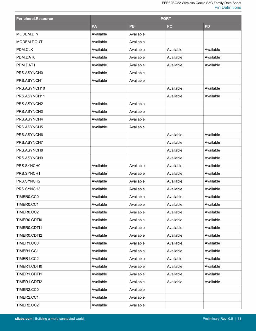
Peripheral.Resource PORT
PA PB PC PD
MODEM.DIN Available Available
MODEM.DOUT Available Available
PDM.CLK Available Available Available Available
PDM.DAT0 Available Available Available Available
PDM.DAT1 Available Available Available Available
PRS.ASYNCH0 Available Available
PRS.ASYNCH1 Available Available
PRS.ASYNCH10 Available Available
PRS.ASYNCH11 Available Available
PRS.ASYNCH2 Available Available
PRS.ASYNCH3 Available Available
PRS.ASYNCH4 Available Available
PRS.ASYNCH5 Available Available
PRS.ASYNCH6 Available Available
PRS.ASYNCH7 Available Available
PRS.ASYNCH8 Available Available
PRS.ASYNCH9 Available Available
PRS.SYNCH0 Available Available Available Available
PRS.SYNCH1 Available Available Available Available
PRS.SYNCH2 Available Available Available Available
PRS.SYNCH3 Available Available Available Available
TIMER0.CC0 Available Available Available Available
TIMER0.CC1 Available Available Available Available
TIMER0.CC2 Available Available Available Available
TIMER0.CDTI0 Available Available Available Available
TIMER0.CDTI1 Available Available Available Available
TIMER0.CDTI2 Available Available Available Available
TIMER1.CC0 Available Available Available Available
TIMER1.CC1 Available Available Available Available
TIMER1.CC2 Available Available Available Available
TIMER1.CDTI0 Available Available Available Available
TIMER1.CDTI1 Available Available Available Available
TIMER1.CDTI2 Available Available Available Available
TIMER2.CC0 Available Available
TIMER2.CC1 Available Available
TIMER2.CC2 Available Available
EFR32BG22 Wireless Gecko SoC Family Data SheetPin Definitions
silabs.com | Building a more connected world. Preliminary Rev. 0.5 | 83
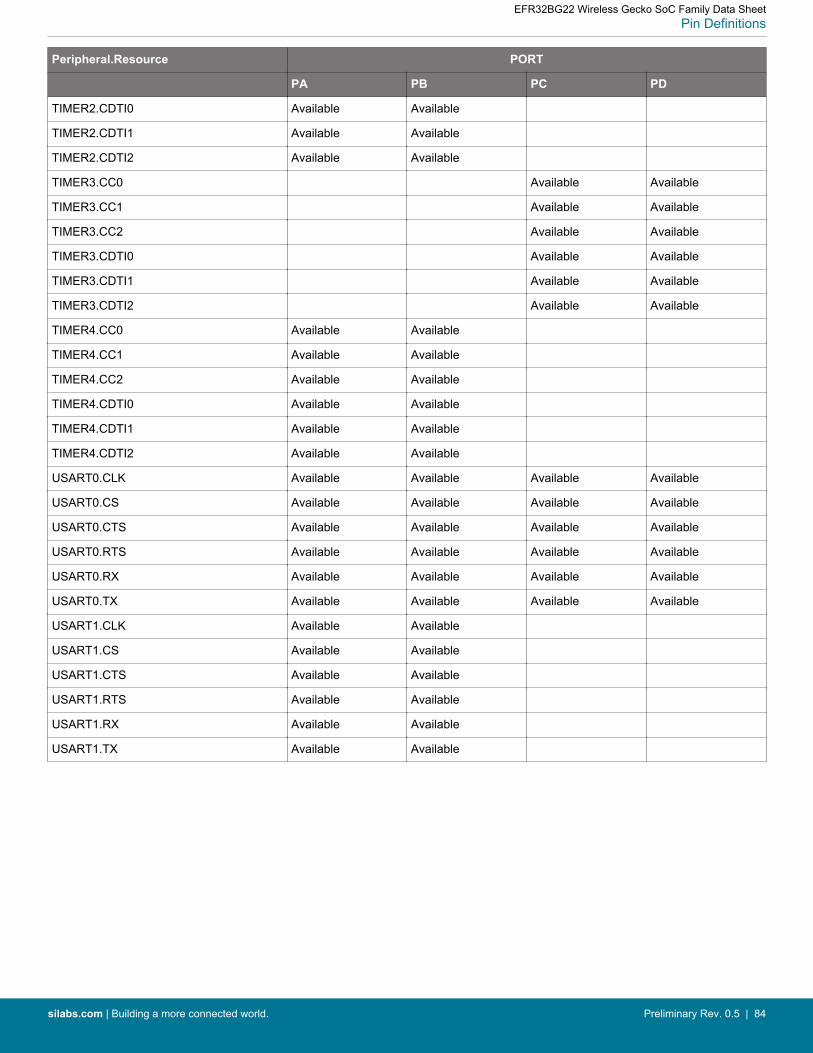
Peripheral.Resource PORT
PA PB PC PD
TIMER2.CDTI0 Available Available
TIMER2.CDTI1 Available Available
TIMER2.CDTI2 Available Available
TIMER3.CC0 Available Available
TIMER3.CC1 Available Available
TIMER3.CC2 Available Available
TIMER3.CDTI0 Available Available
TIMER3.CDTI1 Available Available
TIMER3.CDTI2 Available Available
TIMER4.CC0 Available Available
TIMER4.CC1 Available Available
TIMER4.CC2 Available Available
TIMER4.CDTI0 Available Available
TIMER4.CDTI1 Available Available
TIMER4.CDTI2 Available Available
USART0.CLK Available Available Available Available
USART0.CS Available Available Available Available
USART0.CTS Available Available Available Available
USART0.RTS Available Available Available Available
USART0.RX Available Available Available Available
USART0.TX Available Available Available Available
USART1.CLK Available Available
USART1.CS Available Available
USART1.CTS Available Available
USART1.RTS Available Available
USART1.RX Available Available
USART1.TX Available Available
EFR32BG22 Wireless Gecko SoC Family Data SheetPin Definitions
silabs.com | Building a more connected world. Preliminary Rev. 0.5 | 84
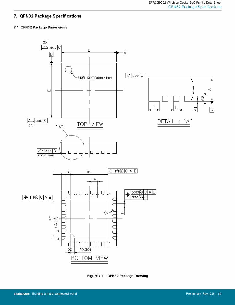
7. QFN32 Package Specifications
7.1 QFN32 Package Dimensions
Figure 7.1. QFN32 Package Drawing
EFR32BG22 Wireless Gecko SoC Family Data SheetQFN32 Package Specifications
silabs.com | Building a more connected world. Preliminary Rev. 0.5 | 85
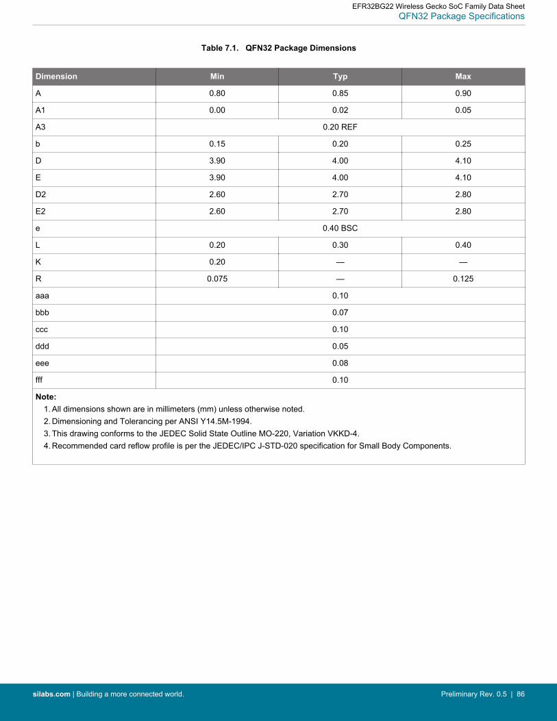
Table 7.1. QFN32 Package Dimensions
Dimension Min Typ Max
A 0.80 0.85 0.90
A1 0.00 0.02 0.05
A3 0.20 REF
b 0.15 0.20 0.25
D 3.90 4.00 4.10
E 3.90 4.00 4.10
D2 2.60 2.70 2.80
E2 2.60 2.70 2.80
e 0.40 BSC
L 0.20 0.30 0.40
K 0.20 — —
R 0.075 — 0.125
aaa 0.10
bbb 0.07
ccc 0.10
ddd 0.05
eee 0.08
fff 0.10
Note:1. All dimensions shown are in millimeters (mm) unless otherwise noted.2. Dimensioning and Tolerancing per ANSI Y14.5M-1994.3. This drawing conforms to the JEDEC Solid State Outline MO-220, Variation VKKD-4.4. Recommended card reflow profile is per the JEDEC/IPC J-STD-020 specification for Small Body Components.
EFR32BG22 Wireless Gecko SoC Family Data SheetQFN32 Package Specifications
silabs.com | Building a more connected world. Preliminary Rev. 0.5 | 86

7.2 QFN32 PCB Land Pattern
Figure 7.2. QFN32 PCB Land Pattern Drawing
EFR32BG22 Wireless Gecko SoC Family Data SheetQFN32 Package Specifications
silabs.com | Building a more connected world. Preliminary Rev. 0.5 | 87
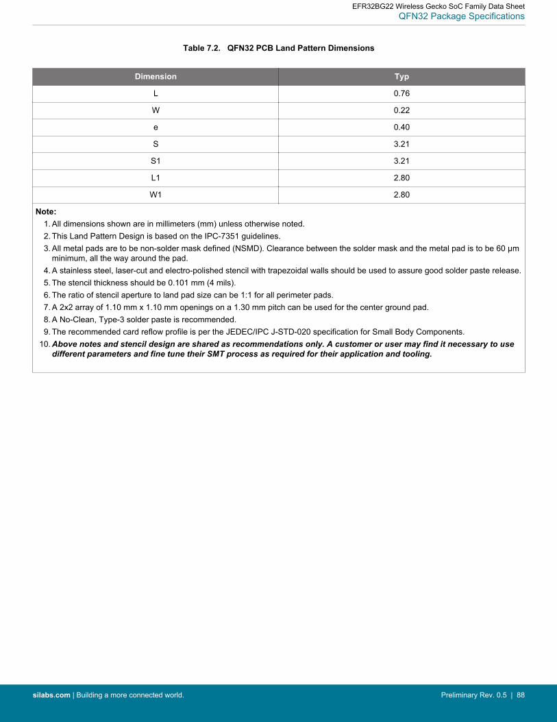
Table 7.2. QFN32 PCB Land Pattern Dimensions
Dimension Typ
L 0.76
W 0.22
e 0.40
S 3.21
S1 3.21
L1 2.80
W1 2.80
Note:1. All dimensions shown are in millimeters (mm) unless otherwise noted.2. This Land Pattern Design is based on the IPC-7351 guidelines.3. All metal pads are to be non-solder mask defined (NSMD). Clearance between the solder mask and the metal pad is to be 60 µm
minimum, all the way around the pad.4. A stainless steel, laser-cut and electro-polished stencil with trapezoidal walls should be used to assure good solder paste release.5. The stencil thickness should be 0.101 mm (4 mils).6. The ratio of stencil aperture to land pad size can be 1:1 for all perimeter pads.7. A 2x2 array of 1.10 mm x 1.10 mm openings on a 1.30 mm pitch can be used for the center ground pad.8. A No-Clean, Type-3 solder paste is recommended.9. The recommended card reflow profile is per the JEDEC/IPC J-STD-020 specification for Small Body Components.
10. Above notes and stencil design are shared as recommendations only. A customer or user may find it necessary to usedifferent parameters and fine tune their SMT process as required for their application and tooling.
EFR32BG22 Wireless Gecko SoC Family Data SheetQFN32 Package Specifications
silabs.com | Building a more connected world. Preliminary Rev. 0.5 | 88
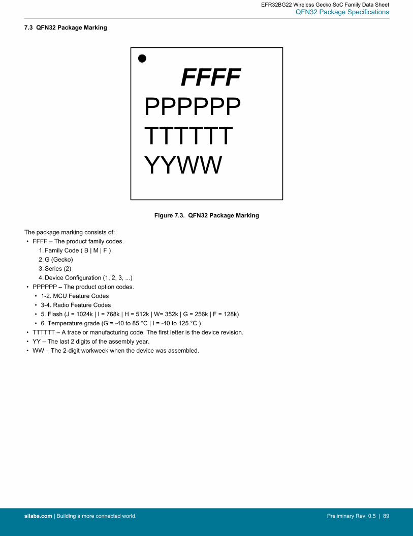
7.3 QFN32 Package Marking
FFFFPPPPPPTTTTTTYYWW
Figure 7.3. QFN32 Package Marking
The package marking consists of:• FFFF – The product family codes.
1. Family Code ( B | M | F )2. G (Gecko)3. Series (2)4. Device Configuration (1, 2, 3, ...)
• PPPPPP – The product option codes.• 1-2. MCU Feature Codes• 3-4. Radio Feature Codes• 5. Flash (J = 1024k | I = 768k | H = 512k | W= 352k | G = 256k | F = 128k)• 6. Temperature grade (G = -40 to 85 °C | I = -40 to 125 °C )
• TTTTTT – A trace or manufacturing code. The first letter is the device revision.• YY – The last 2 digits of the assembly year.• WW – The 2-digit workweek when the device was assembled.
EFR32BG22 Wireless Gecko SoC Family Data SheetQFN32 Package Specifications
silabs.com | Building a more connected world. Preliminary Rev. 0.5 | 89
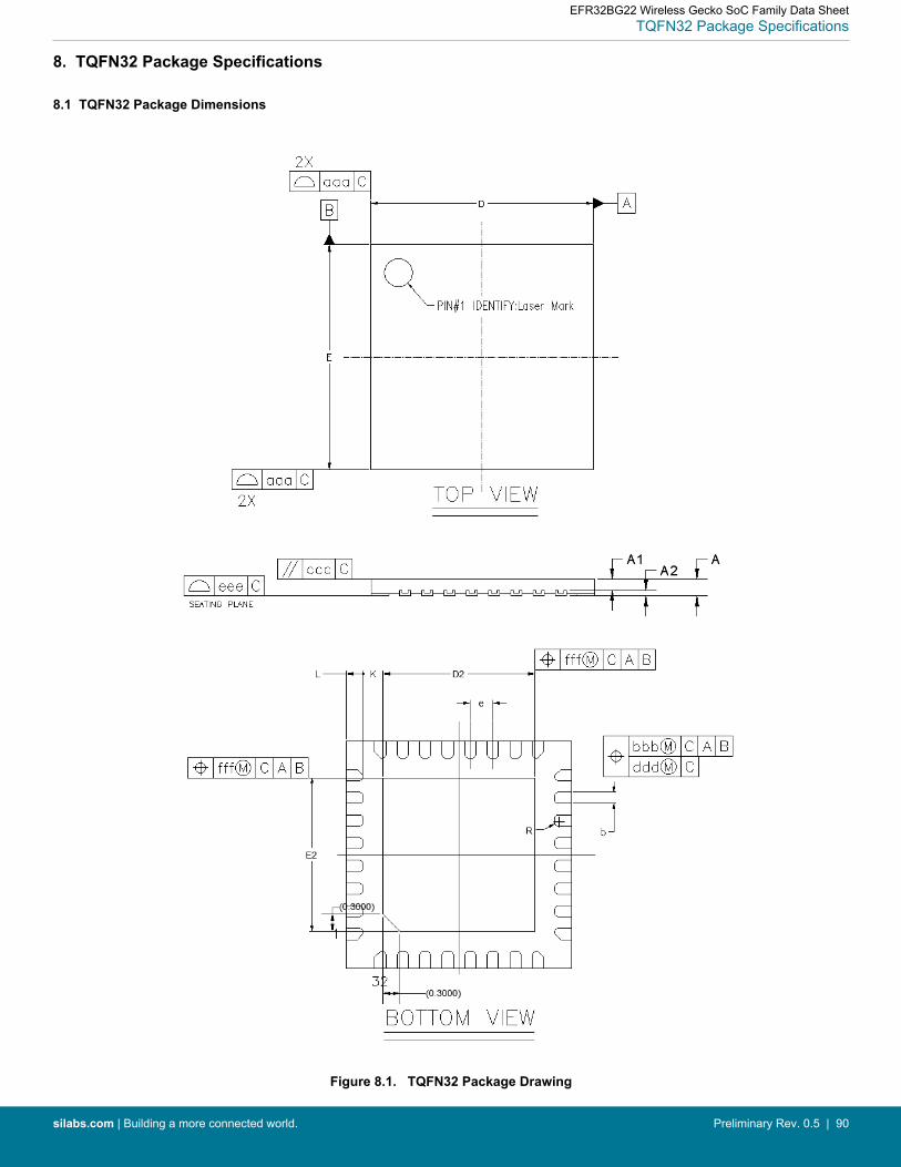
8. TQFN32 Package Specifications
8.1 TQFN32 Package Dimensions
Figure 8.1. TQFN32 Package Drawing
EFR32BG22 Wireless Gecko SoC Family Data SheetTQFN32 Package Specifications
silabs.com | Building a more connected world. Preliminary Rev. 0.5 | 90
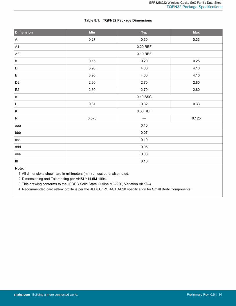
Table 8.1. TQFN32 Package Dimensions
Dimension Min Typ Max
A 0.27 0.30 0.33
A1 0.20 REF
A2 0.10 REF
b 0.15 0.20 0.25
D 3.90 4.00 4.10
E 3.90 4.00 4.10
D2 2.60 2.70 2.80
E2 2.60 2.70 2.80
e 0.40 BSC
L 0.31 0.32 0.33
K 0.33 REF
R 0.075 — 0.125
aaa 0.10
bbb 0.07
ccc 0.10
ddd 0.05
eee 0.08
fff 0.10
Note:1. All dimensions shown are in millimeters (mm) unless otherwise noted.2. Dimensioning and Tolerancing per ANSI Y14.5M-1994.3. This drawing conforms to the JEDEC Solid State Outline MO-220, Variation VKKD-4.4. Recommended card reflow profile is per the JEDEC/IPC J-STD-020 specification for Small Body Components.
EFR32BG22 Wireless Gecko SoC Family Data SheetTQFN32 Package Specifications
silabs.com | Building a more connected world. Preliminary Rev. 0.5 | 91
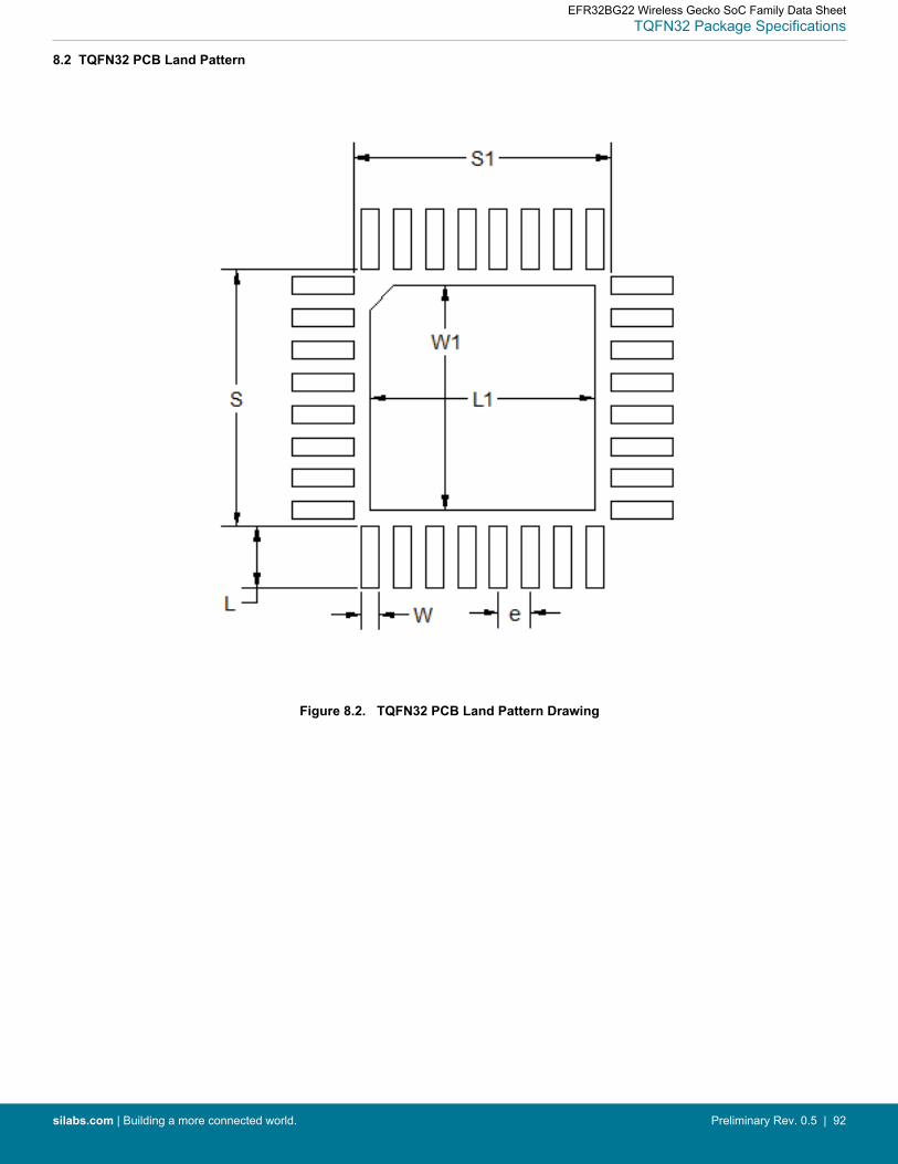
8.2 TQFN32 PCB Land Pattern
Figure 8.2. TQFN32 PCB Land Pattern Drawing
EFR32BG22 Wireless Gecko SoC Family Data SheetTQFN32 Package Specifications
silabs.com | Building a more connected world. Preliminary Rev. 0.5 | 92

Table 8.2. TQFN32 PCB Land Pattern Dimensions
Dimension Typ
L 0.76
W 0.22
e 0.40
S 3.21
S1 3.21
L1 2.80
W1 2.80
Note:1. All dimensions shown are in millimeters (mm) unless otherwise noted.2. This Land Pattern Design is based on the IPC-7351 guidelines.3. All metal pads are to be non-solder mask defined (NSMD). Clearance between the solder mask and the metal pad is to be 60 µm
minimum, all the way around the pad.4. A stainless steel, laser-cut and electro-polished stencil with trapezoidal walls should be used to assure good solder paste release.5. The stencil thickness should be 0.101 mm (4 mils).6. The ratio of stencil aperture to land pad size can be 1:1 for all perimeter pads.7. A 2x2 array of 1.10 mm x 1.10 mm openings on a 1.30 mm pitch can be used for the center ground pad.8. A No-Clean, Type-3 solder paste is recommended.9. The recommended card reflow profile is per the JEDEC/IPC J-STD-020 specification for Small Body Components.
10. Above notes and stencil design are shared as recommendations only. A customer or user may find it necessary to usedifferent parameters and fine tune their SMT process as required for their application and tooling.
EFR32BG22 Wireless Gecko SoC Family Data SheetTQFN32 Package Specifications
silabs.com | Building a more connected world. Preliminary Rev. 0.5 | 93
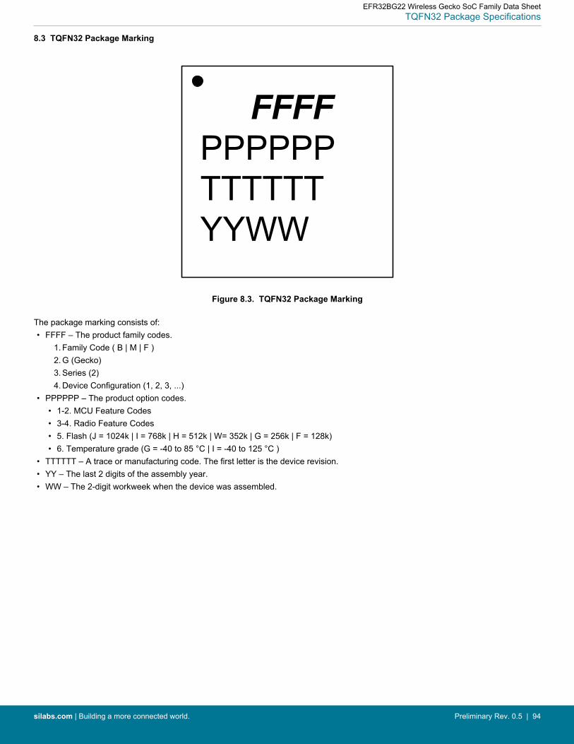
8.3 TQFN32 Package Marking
FFFFPPPPPPTTTTTTYYWW
Figure 8.3. TQFN32 Package Marking
The package marking consists of:• FFFF – The product family codes.
1. Family Code ( B | M | F )2. G (Gecko)3. Series (2)4. Device Configuration (1, 2, 3, ...)
• PPPPPP – The product option codes.• 1-2. MCU Feature Codes• 3-4. Radio Feature Codes• 5. Flash (J = 1024k | I = 768k | H = 512k | W= 352k | G = 256k | F = 128k)• 6. Temperature grade (G = -40 to 85 °C | I = -40 to 125 °C )
• TTTTTT – A trace or manufacturing code. The first letter is the device revision.• YY – The last 2 digits of the assembly year.• WW – The 2-digit workweek when the device was assembled.
EFR32BG22 Wireless Gecko SoC Family Data SheetTQFN32 Package Specifications
silabs.com | Building a more connected world. Preliminary Rev. 0.5 | 94
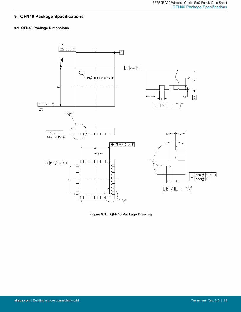
9. QFN40 Package Specifications
9.1 QFN40 Package Dimensions
Figure 9.1. QFN40 Package Drawing
EFR32BG22 Wireless Gecko SoC Family Data SheetQFN40 Package Specifications
silabs.com | Building a more connected world. Preliminary Rev. 0.5 | 95

Table 9.1. QFN40 Package Dimensions
Dimension Min Typ Max
A 0.80 0.85 0.90
A1 0.00 0.02 0.05
A3 0.20 REF
b 0.15 0.20 0.25
D 4.90 5.00 5.10
E 4.90 5.00 5.10
D2 3.55 3.70 3.85
E2 3.55 3.70 3.85
e 0.40 BSC
L 0.30 0.40 0.50
K 0.20 — —
R 0.075 — —
aaa 0.10
bbb 0.07
ccc 0.10
ddd 0.05
eee 0.08
fff 0.10
Note:1. All dimensions shown are in millimeters (mm) unless otherwise noted.2. Dimensioning and Tolerancing per ANSI Y14.5M-1994.3. This drawing conforms to the JEDEC Solid State Outline MO-220, Variation VKKD-4.4. Recommended card reflow profile is per the JEDEC/IPC J-STD-020 specification for Small Body Components.
EFR32BG22 Wireless Gecko SoC Family Data SheetQFN40 Package Specifications
silabs.com | Building a more connected world. Preliminary Rev. 0.5 | 96
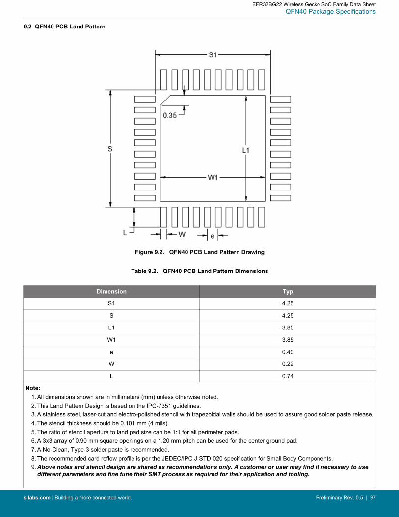
9.2 QFN40 PCB Land Pattern
Figure 9.2. QFN40 PCB Land Pattern Drawing
Table 9.2. QFN40 PCB Land Pattern Dimensions
Dimension Typ
S1 4.25
S 4.25
L1 3.85
W1 3.85
e 0.40
W 0.22
L 0.74
Note:1. All dimensions shown are in millimeters (mm) unless otherwise noted.2. This Land Pattern Design is based on the IPC-7351 guidelines.3. A stainless steel, laser-cut and electro-polished stencil with trapezoidal walls should be used to assure good solder paste release.4. The stencil thickness should be 0.101 mm (4 mils).5. The ratio of stencil aperture to land pad size can be 1:1 for all perimeter pads.6. A 3x3 array of 0.90 mm square openings on a 1.20 mm pitch can be used for the center ground pad.7. A No-Clean, Type-3 solder paste is recommended.8. The recommended card reflow profile is per the JEDEC/IPC J-STD-020 specification for Small Body Components.9. Above notes and stencil design are shared as recommendations only. A customer or user may find it necessary to use
different parameters and fine tune their SMT process as required for their application and tooling.
EFR32BG22 Wireless Gecko SoC Family Data SheetQFN40 Package Specifications
silabs.com | Building a more connected world. Preliminary Rev. 0.5 | 97
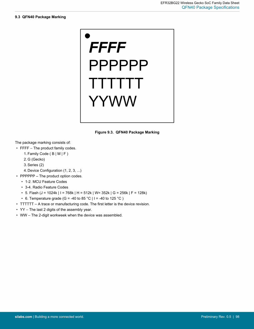
9.3 QFN40 Package Marking
FFFFPPPPPPTTTTTTYYWW
Figure 9.3. QFN40 Package Marking
The package marking consists of:• FFFF – The product family codes.
1. Family Code ( B | M | F )2. G (Gecko)3. Series (2)4. Device Configuration (1, 2, 3, ...)
• PPPPPP – The product option codes.• 1-2. MCU Feature Codes• 3-4. Radio Feature Codes• 5. Flash (J = 1024k | I = 768k | H = 512k | W= 352k | G = 256k | F = 128k)• 6. Temperature grade (G = -40 to 85 °C | I = -40 to 125 °C )
• TTTTTT – A trace or manufacturing code. The first letter is the device revision.• YY – The last 2 digits of the assembly year.• WW – The 2-digit workweek when the device was assembled.
EFR32BG22 Wireless Gecko SoC Family Data SheetQFN40 Package Specifications
silabs.com | Building a more connected world. Preliminary Rev. 0.5 | 98
10. Revision History
Revision 0.5
February, 2020
• 1. Feature List: Updated list slightly to highlight different features.• Expanded 3.7 Security Features section and corrected security details.• Added 3.9.2 Voltage Scaling section.• 4.1 Electrical Characteristics:
• Additional characterization results and test limits added where available.• Removed thermistor driver specification table until full software support becomes available.
• Updated 5.2 RF Matching Networks section with recommended match values.• Updated 9.3 QFN40 Package Marking with mark details.
Revision 0.4
December, 2019
• 4.1 Electrical Characteristics:• Added detailed lifetime information to DC-DC specifications section.• Additional characterization results and preliminary test limits added where available.
• Added DC-DC efficiency plots and updated supply current plots to 4.20 Typical Performance Curves.
Revision 0.3
October, 2019
• In the front page block diagram, updated the lowest energy mode for LETIMER.• Updated 3.5.2 Low Energy Timer (LETIMER) lowest energy mode.• 1. Feature List updated with additional modulation formats, protocol stack, and security details.• 2. Ordering Information:
• OPN numbering changes for security grade differentiator.• Supported protocol stack details updated.
• 4.1 Electrical Characteristics:• Additional characterization results and preliminary test limits added where available.• Corrected maximum clock speed details in General Operating Conditions Table.• Removed specification lines with 3 dBm output power conditions from RF transmit tables.• Removed DECOUPLE BOD table.• Added timing diagrams and specifications for PDM and USART SPI.
• Added 4.20 Typical Performance Curves.
Revision 0.2
July, 2019
• 2. Ordering Information: Updated part number to revision C, added several new variants.• 4.1 Electrical Characteristics: Added early silicon characterization data to several tables, and refined specification conditions.• 4.1 Electrical Characteristics: Added flash electrical characteristics table.• Minor wording edits for System Overview sections.
Revision 0.1
April, 2019
Initial release.
EFR32BG22 Wireless Gecko SoC Family Data SheetRevision History
silabs.com | Building a more connected world. Preliminary Rev. 0.5 | 99

Simplicity StudioOne-click access to MCU and wireless tools, documentation, software, source code libraries & more. Available for Windows, Mac and Linux!
IoT Portfoliowww.silabs.com/IoT
SW/HWwww.silabs.com/simplicity
Qualitywww.silabs.com/quality
Support and Communitycommunity.silabs.com
http://www.silabs.com
Silicon Laboratories Inc.400 West Cesar ChavezAustin, TX 78701USA
DisclaimerSilicon Labs intends to provide customers with the latest, accurate, and in-depth documentation of all peripherals and modules available for system and software implementers using or intending to use the Silicon Labs products. Characterization data, available modules and peripherals, memory sizes and memory addresses refer to each specific device, and "Typical" parameters provided can and do vary in different applications. Application examples described herein are for illustrative purposes only. Silicon Labs reserves the right to make changes without further notice to the product information, specifications, and descriptions herein, and does not give warranties as to the accuracy or completeness of the included information. Without prior notification, Silicon Labs may update product firmware during the manufacturing process for security or reliability reasons. Such changes will not alter the specifications or the performance of the product. Silicon Labs shall have no liability for the consequences of use of the information supplied in this document. This document does not imply or expressly grant any license to design or fabricate any integrated circuits. The products are not designed or authorized to be used within any FDA Class III devices, applications for which FDA premarket approval is required, or Life Support Systems without the specific written consent of Silicon Labs. A "Life Support System" is any product or system intended to support or sustain life and/or health, which, if it fails, can be reasonably expected to result in significant personal injury or death. Silicon Labs products are not designed or authorized for military applications. Silicon Labs products shall under no circumstances be used in weapons of mass destruction including (but not limited to) nuclear, biological or chemical weapons, or missiles capable of delivering such weapons. Silicon Labs disclaims all express and implied warranties and shall not be responsible or liable for any injuries or damages related to use of a Silicon Labs product in such unauthorized applications.
Trademark InformationSilicon Laboratories Inc.®, Silicon Laboratories®, Silicon Labs®, SiLabs® and the Silicon Labs logo®, Bluegiga®, Bluegiga Logo®, ClockBuilder®, CMEMS®, DSPLL®, EFM®, EFM32®, EFR, Ember®, Energy Micro, Energy Micro logo and combinations thereof, "the world’s most energy friendly microcontrollers", Ember®, EZLink®, EZRadio®, EZRadioPRO®, Gecko®, Gecko OS, Gecko OS Studio, ISOmodem®, Precision32®, ProSLIC®, Simplicity Studio®, SiPHY®, Telegesis, the Telegesis Logo®, USBXpress® , Zentri, the Zentri logo and Zentri DMS, Z-Wave®, and others are trademarks or registered trademarks of Silicon Labs. ARM, CORTEX, Cortex-M3 and THUMB are trademarks or registered trademarks of ARM Holdings. Keil is a registered trademark of ARM Limited. Wi-Fi is a registered trademark of the Wi-Fi Alliance. All other products or brand names mentioned herein are trademarks of their respective holders.
![ABYG 30, 36 I 45 ABYG 36, 45, 54 [3PH] ALL - …...ABYG 30, 36 I 45 ABYG 36, 45, 54 [3PH] ALL i-PAM MODEL DOUBLE SWING ADJUST AUTO RESTART AUTO CHANGEOVER SLEEP TIMER PROGRAM TIMER](https://img.pdfslide.us/doc/110x75/5f13de77a346fe3331726309/abyg-30-36-i-45-abyg-36-45-54-3ph-all-abyg-30-36-i-45-abyg-36-45-54.jpg)