Embed Size (px)
Citation preview
International Journal of Scientific and Research Publications, Volume 3, Issue 4, April 2013 1 ISSN 2250-3153
www.ijsrp.org
Efficient Flash Translation layer for Flash Memory
Shinde Pratibha*, Mrs.Suvarna
**
* PG student, Department of IT-PDVVP COE, Pune University, Ahmednagar
** Asst.Professor, Department of IT-RM COE, JNT University, Hyderabad
Abstract- Flash is a type of electronically erasable programmable
read- only memory (EEPROM). Flash memory is important as
nonvolatile storage for mobile consumer electronics due to its
low power consumption and shock resistance.
NAND flash memory has many advantageous features as a
storage medium, such as superior performance, shock resistance,
and low power consumption. However, the erase-before-write
nature and the limited number of write/erase cycles are obstacles
to the promising future of NAND flash memory. An intermediate
software layer called Flash Translation Layer (FTL) is used to
overcome these obstacles.
Many efforts for optimizing the working of address
mapping schemes have been done by different research
workers. Though various schemes are designed and proposed but
there is no literature available providing mathematical
computations comparing the performance of the various mapping
schemes in the form of time complexity. In this paper we have
tried to find out the comparative cost of block merge operation
required during garbage collection for some representative
mapping schemes like BAST and FAST .
I. INTRODUCTION
1.1 Characteristics of NAND flash memory
NAND flash memory has several limitations:
1) The previous data should be erased before a new data
can be written in the same place. This is usually called erase-
before-write characteristic.
2) Normal read/write operations are performed on a per-
page basis, while erase operations on a per-block basis. The erase
block size is larger than the page size by 64~128 times. In MLC
(Multi-Level Cell) NAND flash memory, the typical page size is
4KB and each block consists of 128 pages.
3) Flash memory has limited lifetime; MLC NAND flash
memory wears out after 5K to 10K write/erase cycles.
There are three basic operations in NAND flash memory: read,
write (or program), and erase. The read operation fetches data
from a target page, while the write operation writes data to a
page. The erase operation resets all values of a target block to 1.
NAND flash memory does not support in-place update.
A NAND flash memory chip is composed of a fixed
number of blocks, where each block typically has 32 pages. Each
page in turn consists of 512 bytes of the main data area and 16
bytes of the spare area. The page is the basic unit of read and
write operations in NAND flash memory.
NAND flash memory is usually used as a storage medium
in place of Hard Disk Drive (HDD) because of its non- volatility
and large I/O unit. It is not straightforward to replace HDDs
with NAND flash memory due to its erase before- write nature.
The erase unit (called block) is larger than the read and write unit
(called page) by 32 – 128 times.
Other semiconductor devices such as SRAMs and DRAMs,
the write operation compared to the read operation. As the write
operation usually accompanies the erase operation.
Another limitation of NAND flash memory is that the
number of program/erase cycles for a block is limited to about
100,000 – 1,000,000 times. Thus, the number of erase operations
should be minimized to improve the overall performance and
the lifetime of NAND flash memory.
1.2 Flash Translation Layer (FTL)
The FTL is one of the core engines in flash-based SSDs
that maintain a mapping table of virtual addresses from upper
layers to physical addresses on the flash.
The main goal of FTL is to emulate the functionality of a
normal block device with flash memory, hiding the presence of
erase operation and erase-before-write characteristics. Two
important functions of FTL are address translation and garbage
collection.
Figure 1 Architecture of Flash File System
Fig. 1 shows the software architecture of the flash file
system. This section focuses on the FTL layer shown in Fig. 1.
The file system layer issues a series of read or write commands
each with a logical sector number, to read data from, or write
data to, specific addresses in flash memory. The logical sector
number is converted to a real physical sector number of flash
memory by some mapping algorithm in the FTL layer.
N
International Journal of Scientific and Research Publications, Volume 3, Issue 4, April 2013 2
ISSN 2250-3153
www.ijsrp.org
FTLs can be categorized into two classes according to their
mapping granularities: Sector-mapped FTLs and block-mapped
FTLs. A Sector-mapped FTL literally maps a logical address into
a physical address in a page unit. It is highly flexible as a logical
page can be written to any physical page in NAND flash
memory. On the other hand, the mapping unit of a block-mapped
FTL is a block. And later on a hybrid mapping scheme proposed
by D. Park came into existence.
II. TYPES OF MAPPING SCHEMES
2.1 Sector – Mapping FTL
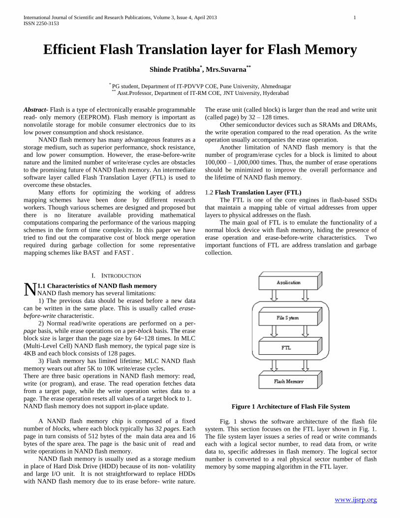
For example, Figure 2 shows an example of sector
mapping. In the example, we assume that a block is composed of
four pages and so there are totally 16 physical pages, where each
page is organized into the sector and spare areas. If we also
assume that there are 16 logical sectors, the row size of the
mapping table is 16. When the file system issues a command -
“write some data to LSN (Logical Sector Number) 9”, the FTL
algorithm writes the data to PSN (Physical Sector Number) 3
according to the mapping table in case the PSN 3 has not
been written before.
Figure 2 Sector Mapping
But, in other case, the FTL algorithm looks for an empty
physical sector, writes data to it, and adjusts the mapping table.
If there is no empty sector, the FTL algorithm will select a victim
block from flash memory, copy back the valid data to the spare
free block, and update the mapping table. Finally, it will erase
the victim block, which will become the spare block.
In order to rebuild the mapping table after power outage,
the FTL algorithm either stores the mapping table to flash
memory or records the logical sector number in the spare area
on each writes to the sector area.
Table 1. Measures of Sector mapping scheme
Garbage collection cost Block Erase is done
when a block is
completely utilized.
RAM requirement Proportional to flash size
Search time Not required
Usefulness Useful in case strict time
requirement
2.2 Block-mapping FTL
The pure block-mapping FTL is another classic FTL
scheme Block-mapping table is used to store and manage the
mapping information between LBN and Physical Block Number
(PBN). If there are m pages in a block, the size of the block-
mapping table is m times smaller than its page-mapping
counterpart. In a block-mapping FTL, one LPN must be mapped
to a fixed page offset in any physical block (i.e., direct mapping).
If this page offset has been written before, the LPN cannot be
written to any other page in this block even if there are free pages
in the same physical block. In this case, all existing valid data in
the block as well as the data to be written must be copied to a
new clean block, and the old block is marked for erase, incurring
one erase and a number of read/write operations. Compared with
the page-mapping FTL the block-mapping FTL requires extra
operations to serve a request, adversely affecting the
performance. Since both the block-mapping and page-mapping
FTLs have their aforementioned disadvantages, they are rarely
used in SSD commercial products in their pure forms.
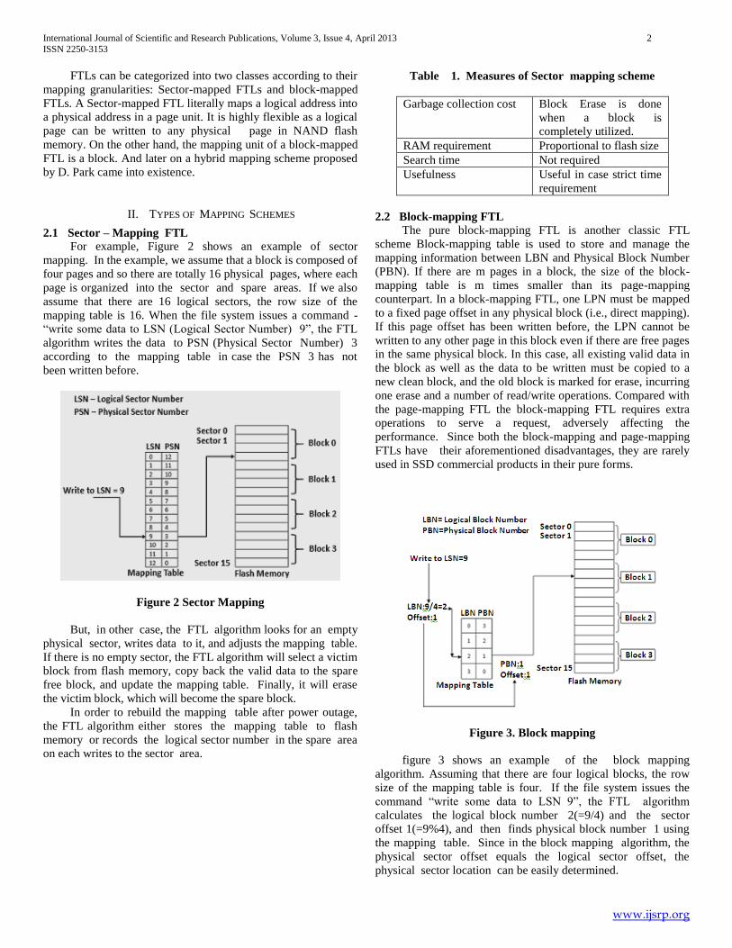
Figure 3. Block mapping
figure 3 shows an example of the block mapping
algorithm. Assuming that there are four logical blocks, the row
size of the mapping table is four. If the file system issues the
command “write some data to LSN 9”, the FTL algorithm
calculates the logical block number 2(=9/4) and the sector
offset 1(=9%4), and then finds physical block number 1 using
the mapping table. Since in the block mapping algorithm, the
physical sector offset equals the logical sector offset, the
physical sector location can be easily determined.
International Journal of Scientific and Research Publications, Volume 3, Issue 4, April 2013 3
ISSN 2250-3153
www.ijsrp.org
Table 2. Measures of block mapping scheme
Garbage collection cost
Block Erase is done hen
a block is completely
utilized.
RAM requirement Proportional to flash size
Search time
Not required
Usefulness
Useful in case of strict
time requirement
2.3 Hybrid FTL
A family of the hybrid mapping schemes is introduced to
address the shortcomings of the Sector-mapping and block-
mapping FTLs. In a typical hybrid FTL, physical blocks are
logically partitioned into two groups: data blocks and log blocks.
When a write request arrives, the hybrid FTL first writes the new
data in a log block and invalidates the data in the corresponding
target data block.
Block-mapping information for data blocks and page-
mapping information for log blocks are kept in a small RAM for
performance purposes. When all the log blocks are full, their data
are flushed into the data blocks immediately and they are then
erased to generate new free log blocks. More specifically, the
valid data in data blocks and the valid data in the corresponding
log block must be merged and written to a new clean data block.
This process is called a merge operation. Further, merge
operations can be classified into three types depending on their
overhead. Full merge occurs, when the log block is selected as a
victim block and not written sequentially from the first page to
the last page, and all the valid data in it and in its corresponding
data block are copied to a new clean block.
This process requires m read operations, m write operations
and two erase operations, where m is the number of pages in a
block. When the log block is written sequentially from the first
page to the last page of a logical block, this log block can replace
the corresponding data block, a merge operation called switch
merge. This type of merge requires only one erase operation.
Partial merge takes place when the log block is written
sequentially from the first page to a middle page in a block, and
the last part of data will be copied from the corresponding data
block. Partial merge requires several read and write operations
and one erase operation. A number of variations of the hybrid
FTL schemes have been proposed recently, including BAST,
FAST, LAST, Superblock Reconfigurable FTL. More recently,
Demand-based FTL (DFTL) was proposed to address the RAM-
capacity problem of the page-mapping FTL by storing only the
“hot” mapping information in RAM based on temporal locality
of workloads.
DFTL is shown to significantly outperform hybrid FTLs.
A hybrid technique, as its name suggests, first uses a block
mapping technique to get the corresponding physical block ,
and then, uses a sector mapping technique to find an available
empty sector within the physical block.
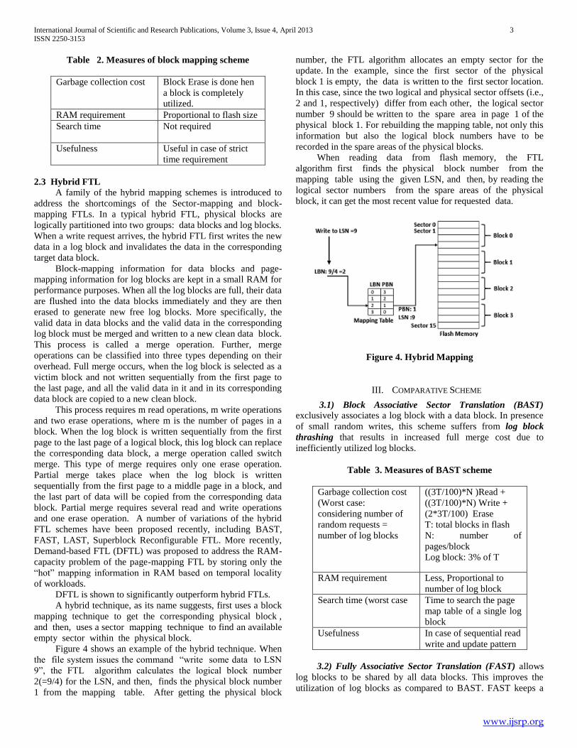
Figure 4 shows an example of the hybrid technique. When
the file system issues the command “write some data to LSN
9”, the FTL algorithm calculates the logical block number
2(=9/4) for the LSN, and then, finds the physical block number
1 from the mapping table. After getting the physical block
number, the FTL algorithm allocates an empty sector for the
update. In the example, since the first sector of the physical
block 1 is empty, the data is written to the first sector location.
In this case, since the two logical and physical sector offsets (i.e.,
2 and 1, respectively) differ from each other, the logical sector
number 9 should be written to the spare area in page 1 of the
physical block 1. For rebuilding the mapping table, not only this
information but also the logical block numbers have to be
recorded in the spare areas of the physical blocks.
When reading data from flash memory, the FTL
algorithm first finds the physical block number from the
mapping table using the given LSN, and then, by reading the
logical sector numbers from the spare areas of the physical
block, it can get the most recent value for requested data.
Figure 4. Hybrid Mapping
III. COMPARATIVE SCHEME
3.1) Block Associative Sector Translation (BAST)
exclusively associates a log block with a data block. In presence
of small random writes, this scheme suffers from log block
thrashing that results in increased full merge cost due to
inefficiently utilized log blocks.
Table 3. Measures of BAST scheme
Garbage collection cost
(Worst case:
considering number of
random requests =
number of log blocks
((3T/100)*N )Read +
((3T/100)*N) Write +
(2*3T/100) Erase
T: total blocks in flash
N: number of
pages/block
Log block: 3% of T
RAM requirement Less, Proportional to
number of log block
Search time (worst case Time to search the page
map table of a single log
block
Usefulness
In case of sequential read
write and update pattern
3.2) Fully Associative Sector Translation (FAST) allows
log blocks to be shared by all data blocks. This improves the
utilization of log blocks as compared to BAST. FAST keeps a
International Journal of Scientific and Research Publications, Volume 3, Issue 4, April 2013 4
ISSN 2250-3153
www.ijsrp.org
single sequential log block dedicated for sequential updates while
other log blocks are used for performing random writes. Thus, it
cannot accommodate multiple sequential streams and does not
provide any special mechanism to handle temporal locality in
random streams.
Table 4. Measures of FAST mapping scheme
Garbage collection cost
(worst and best case :
considering number of
random requests =
K* number of log
Blocks)
((3T/100)*K*N) Read +
((3T/100) * K*N) Write
+(2*3T/100) Erase
T: total blocks in flash
N: number of ages/block
Log block: 3% of T
RAM requirement Less, Proportional to
num, of random log
blocks
Search time (worst
case)
Time to search the page
map table of all log
blocks.
Usefulness
3.3) Super Block FTL scheme utilizes existence of block
level spatial locality in workloads by combining consecutive
logical blocks into a super block. It maintains page- level
mappings within the superblock to exploit temporal locality in
the request streams by separating hot and cold data within the
superblock. However, the three-level address translation
mechanism employed by this scheme causes multiple OOB area
reads and writes for servicing the requests. More importantly, it
utilizes a fixed superblock size which needs to be explicitly tuned
to adapt to changing workload requirements.
3.4) Locality-Aware Sector Translation (LAST)
Scheme tries to alleviate the shortcomings of FAST by
providing multiple sequential log blocks to exploit spatial
locality in workloads. It further separates random log blocks into
hot and cold regions to reduce full merge cost. In order to
provide this dynamic separation, LAST depends on an external
locality detection mechanism. However, Lee et al. themselves
realize that the proposed locality detector cannot efficiently
identify sequential writes when the small-sized write has
sequential locality. Moreover, maintaining sequential log blocks
using a block-based mapping table requires the sequential
streams to be aligned with the starting page offset of the log
block in order to perform switch-merge. Dynamically changing
request streams may impose severe restrictions on the utility of
this scheme to efficiently adapt to the workload patterns.
Table 5. Measures of LAST mapping scheme
Garbage collection cost Better than FAST
RAM requirement Same as that of FAST
Search time Time to search a page
map tables of all log
block
Usefulness Useful in case of random
Read write & update
pattern.
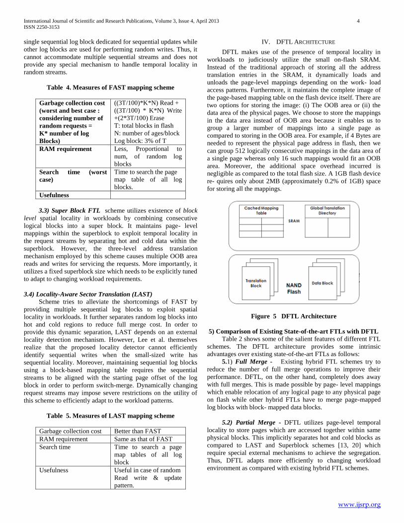
IV. DFTL ARCHITECTURE
DFTL makes use of the presence of temporal locality in
workloads to judiciously utilize the small on-flash SRAM.
Instead of the traditional approach of storing all the address
translation entries in the SRAM, it dynamically loads and
unloads the page-level mappings depending on the work- load
access patterns. Furthermore, it maintains the complete image of
the page-based mapping table on the flash device itself. There are
two options for storing the image: (i) The OOB area or (ii) the
data area of the physical pages. We choose to store the mappings
in the data area instead of OOB area because it enables us to
group a larger number of mappings into a single page as
compared to storing in the OOB area. For example, if 4 Bytes are
needed to represent the physical page address in flash, then we
can group 512 logically consecutive mappings in the data area of
a single page whereas only 16 such mappings would fit an OOB
area. Moreover, the additional space overhead incurred is
negligible as compared to the total flash size. A 1GB flash device
re- quires only about 2MB (approximately 0.2% of 1GB) space
for storing all the mappings.
Figure 5 DFTL Architecture
5) Comparison of Existing State-of-the-art FTLs with DFTL Table 2 shows some of the salient features of different FTL
schemes. The DFTL architecture provides some intrinsic
advantages over existing state-of-the-art FTLs as follows:
5.1) Full Merge - Existing hybrid FTL schemes try to
reduce the number of full merge operations to improve their
performance. DFTL, on the other hand, completely does away
with full merges. This is made possible by page- level mappings
which enable relocation of any logical page to any physical page
on flash while other hybrid FTLs have to merge page-mapped
log blocks with block- mapped data blocks.
5.2) Partial Merge - DFTL utilizes page-level temporal
locality to store pages which are accessed together within same
physical blocks. This implicitly separates hot and cold blocks as
compared to LAST and Superblock schemes [13, 20] which
require special external mechanisms to achieve the segregation.
Thus, DFTL adapts more efficiently to changing workload
environment as compared with existing hybrid FTL schemes.
International Journal of Scientific and Research Publications, Volume 3, Issue 4, April 2013 5
ISSN 2250-3153
www.ijsrp.org
5.3) Random Write Performance - As is clearly evident, it
is not necessarily the random writes which cause poor flash
device performance but the intrinsic shortcomings in the design
of hybrid FTLs which cause costly merges (full) on log blocks
during garbage collection. Since DFTL does not require these
expensive full-merges, it is able to improve random write
performance.
5.4) Block Utilization - In hybrid FTLs, only log blocks are
available for servicing update requests. This can lead to low
block utilization for workloads whose working-set size is smaller
than the flash size. Many data blocks will remain un-utilized
(hybrid FTLs have block-based map- pings for data blocks) and
unnecessary garbage collection will be performed. DFTL solves
this problem since up- dates can be performed on any of the data
blocks.
V. CONCLUSION
We argued that existing hybrid FTL schemes exhibit poor
performance for enterprise-scale workloads with significant
random write patterns. We proposed a complete paradigm shift in
the design of the FTL with our Demand-based Flash Translation
Layer (DFTL) that selectively caches page- level address
mappings. Our experimental evaluation using Disk Sim with
realistic enterprise-scale workloads endorsed DFTL’s efficacy
for enterprise systems by demonstrating that DFTL offered (i)
Improved performance, (ii) reduced garbage collection overhead,
(iii) Improved overload behavior and (iv) Most importantly
unlike existing hybrid FTLs is free from any tunable parameters.
As a representative example, a predominantly random write-
dominant I/O trace from an OLTP application running at a large
financial institution showed a 78% improvement in average
response time due to a 3-fold reduction in garbage collection
induced operations as compared to a state-of-the-art FTL
scheme.
Table 6. Comparative analysis of various FTL schemes
FTL
Scheme
Merg
e cost
of
block
durin
g GC
Lookup
performanc
e
RAM
req.
Mapping
granularity
Pure
page
level
N/A No lookup
cost
Much
more
Page
Pure
block
level
Much
more
No lookup
cost
Very
less
Block
BAST More Less Less Page for log
blocks.
Blocks for
data blocks
FAST Lesse
r than
BAS
T
Much more Less Page for log
blocks.
Blocks for
data blocks
LAST Lesse
r than
FAST
Much more Less Page & block
for log
blocks. Block
for data
blocks
Demand
paged
N/A Lesser Lesse
r
Page
REFERENCES
[1] Tae-Sun Chung, Dong-Joo Park, Sangwon Park, Dong-Ho Lee, Sang-Won Lee, Ha-Joo Song “A survey of Flash Translation Layer” College of Information Technology, Ajou University, Suwon 443-749, Korea School of Computing, Soongsil University, Seoul 156-743, Korea Information Comm- unication Engineering, Hankook University of Foreign Studies, Yongin 449-791, Korea.
[2] Jeong-UK Kang ,Heeseung Jo , Jin-Soo Kim, Joonwon Lee “A Superblock based Flash Translation layer for NAND Flash Memory” Computer Science Division Korea Advanced Instituteof Science & Technology(KAIST) Daejeon ,Korea.
[3] C.Association. http://www.compactflash.org/.
[4] A. Ban. Flash file system. United States Patent, no. 5, 404,485, April 1995.
[5] I. Corporation. Understanding the flash translation layer (ftl) specification. http://developer.intel.com/.
[6] Aayush Gupta Youngjae Kim Bhuvan Urngaonkar “DFTL: A Flash Translation Layer Employing Demand-based Selective Caching of Page-level Address Mappings” Computer Systems Laboratory, department of Computer Science & Engineering. The Pennsylvania State University, Univesity Park,PA 16802, Technical Report CSE-08-012 August 2008.
[7] Dongchul Park, Biplob Debnath, and David Du “CFTL: A Convertible Flash Translation Layer with Consideration of Data Access Patterns”, Technical Report Department of Computer Science and Engineering University of Minnesota September 14, 2009.
[8] S. Lee, D. Shin, Y. Kim, and J. Kim. LAST: Locality- Aware Sector Translation for NAND Flash Memory- Based Storage Systems, in Proceedings of the International Workshop on Storage and I/O Virtualization, Performance, Energy, Evaluation and Dependability (SPEED2008), February 2008.
[9] S. Lee, D. Park, T. Chung, D. Lee, S. Park, and H. Song. A Log Buffer based Flash Translation Layer Using Fully Asso-ciative Sector Translation.
International Journal of Scientific and Research Publications, Volume 3, Issue 4, April 2013 6
ISSN 2250-3153
www.ijsrp.org
IEEE Transactions on Embedded Computing Systems, 6(3):18, 2007. ISSN 1539–9087.
[10] J. Kang, H. Jo, J. Kim, and J. Lee. A Superblock-based Flash Translation Layer for NAND Flash Memory. In Proceedings of the International Conference on Embedded Software (EM-SOFT), pages 161–170, October 2006. ISBN 1-59593-542-8.
[11] Chung, D. Park, S . Park, D. Lee, S. Lee, and H. Song. System Software for Flash Memory: A Survey. In Proceedings of the International Conference on Embedded and Ubiquitous Computing, pages 394–404, August 2006.
AUTHORS
First Author – Shinde Pratibha, PG student, Department of IT-
PDVVP COE, Pune University, Ahmednagar, Email: [email protected]
Second Author – Mrs.Suvarna, Asst.Professor, Department of
IT-RM COE, JNT University, Hyderabad, Email: [email protected]