Embed Size (px)
Citation preview

Efficient Data Mapping andBuffering Techniques for
Multi-Level CellPhase-Change Memories
HanBin Yoon, Justin Meza,Naveen Muralimanohar*, Onur Mutlu, Norm Jouppi*†
Carnegie Mellon University * Hewlett-Packard Labs † Google, Inc.

2
Executive Summary Phase-change memory (PCM) is a promising emerging technology
More scalable than DRAM, faster than flash Multi-level cell (MLC) PCM = multiple bits per cell → high density
Problem: Higher latency/energy compared to non-MLC PCM Observation: MLC bits have asymmetric read/write characteristics
Some bits can be read quickly but written slowly and vice versa

3
Executive Summary Goal: Read data from fast-read bits; write data to fast-write bits Solution:
Decouple bits to expose fast-read/write memory regions Map read/write-intensive data to appropriate memory regions Split device row buffers to leverage decoupling for better locality
Result:– Improved performance (+19.2%) and energy efficiency (+14.4%)– Across SPEC CPU2006 and data-intensive/cloud workloads
4
Outline Background Problem and Goal Key Observations
– MLC-PCM cell read asymmetry– MLC-PCM cell write asymmetry
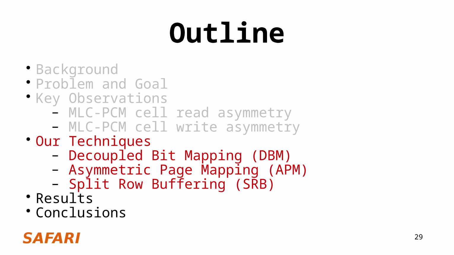
Our Techniques– Decoupled Bit Mapping (DBM)– Asymmetric Page Mapping (APM)– Split Row Buffering (SRB)
Results Conclusions

5
Background: PCM Emerging high-density memory technology
– Potential for scalable DRAM alternative• Projected to be 3 to 12x denser than DRAM• Access latency within an order or magnitude of DRAM
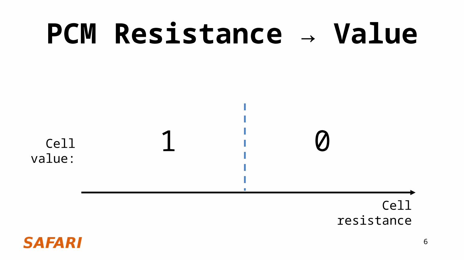
Stores data in the form of resistance of cell material
6
PCM Resistance → Value
Cell resistance
1 0Cell value:

7
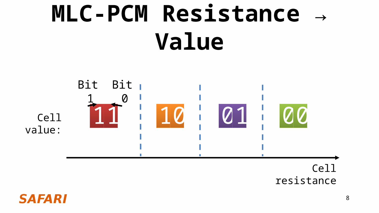
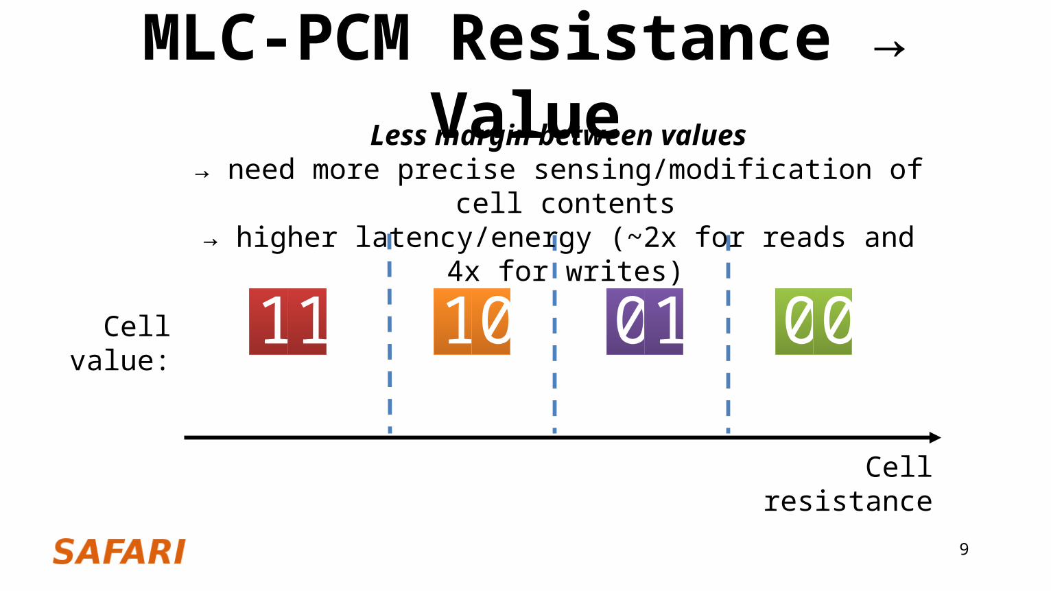
Background: MLC-PCM Multi-level cell: more than 1 bit per cell
Further increases density by 2 to 4x [Lee+,ISCA'09]
But MLC-PCM also has drawbacks Higher latency and energy than single-level cell PCM Let's take a look at why this is the case
8
MLC-PCM Resistance → Value
Cell resistance
11 000110Cell value:
Bit 1 Bit 0
9
MLC-PCM Resistance → Value
Cell resistance
11 000110Cell value:
Less margin between values→ need more precise sensing/modification of cell contents→ higher latency/energy (~2x for reads and 4x for writes)

10
Problem and Goal Want to leverage MLC-PCM's strengths
– Higher density– More scalability than existing technologies (DRAM)
But, also want to mitigate MLC-PCM's weaknesses– Higher latency/energy
Our goal in this work is to design new hardware/software optimizations designed to mitigate the weaknesses of MLC-PCM
11
Outline Background Problem and Goal Key Observations
– MLC-PCM cell read asymmetry– MLC-PCM cell write asymmetry
Our Techniques– Decoupled Bit Mapping (DBM)– Asymmetric Page Mapping (APM)– Split Row Buffering (SRB)
Results Conclusions
12
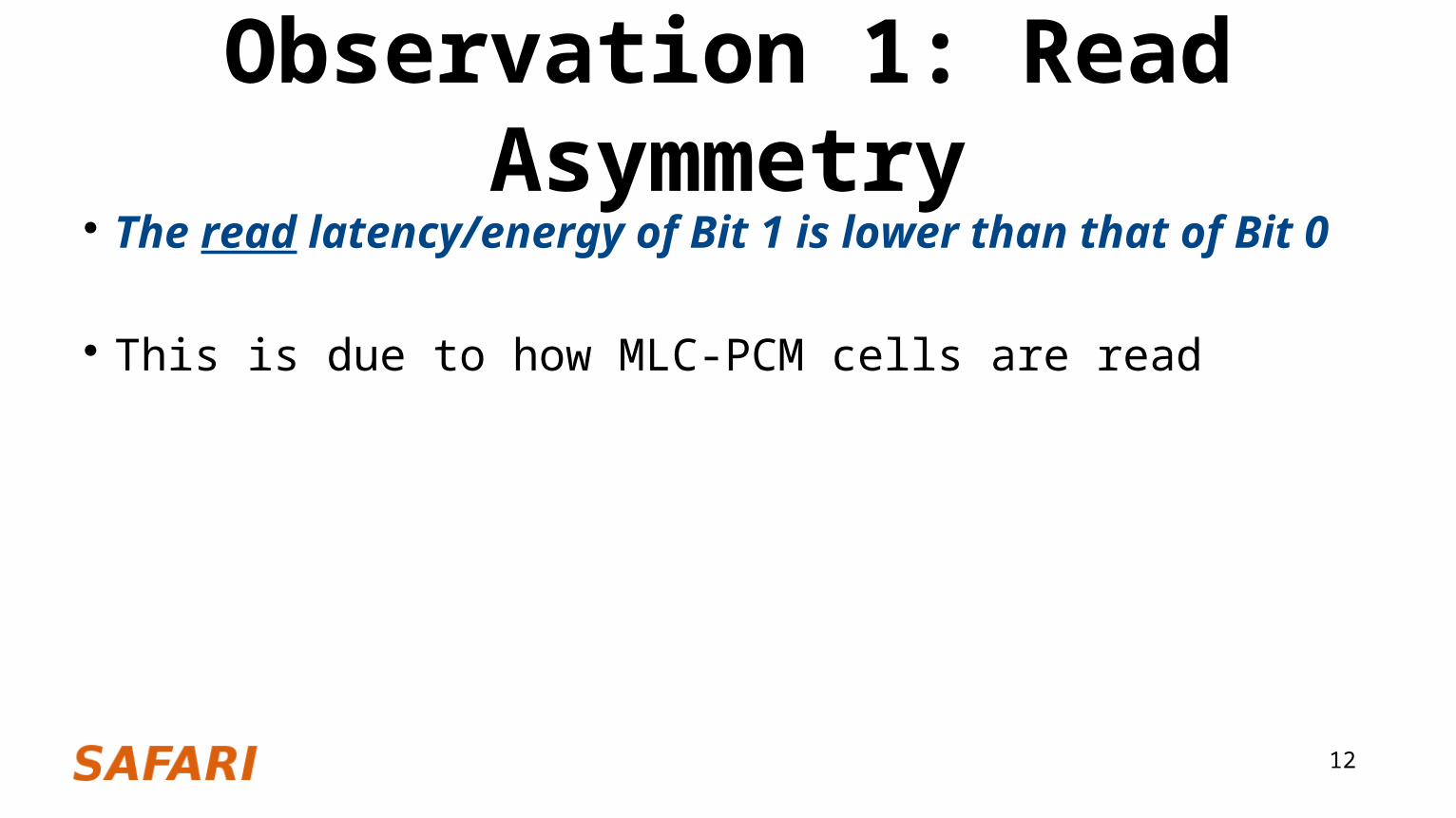
Observation 1: Read Asymmetry The read latency/energy of Bit 1 is lower than that of Bit 0
This is due to how MLC-PCM cells are read

13
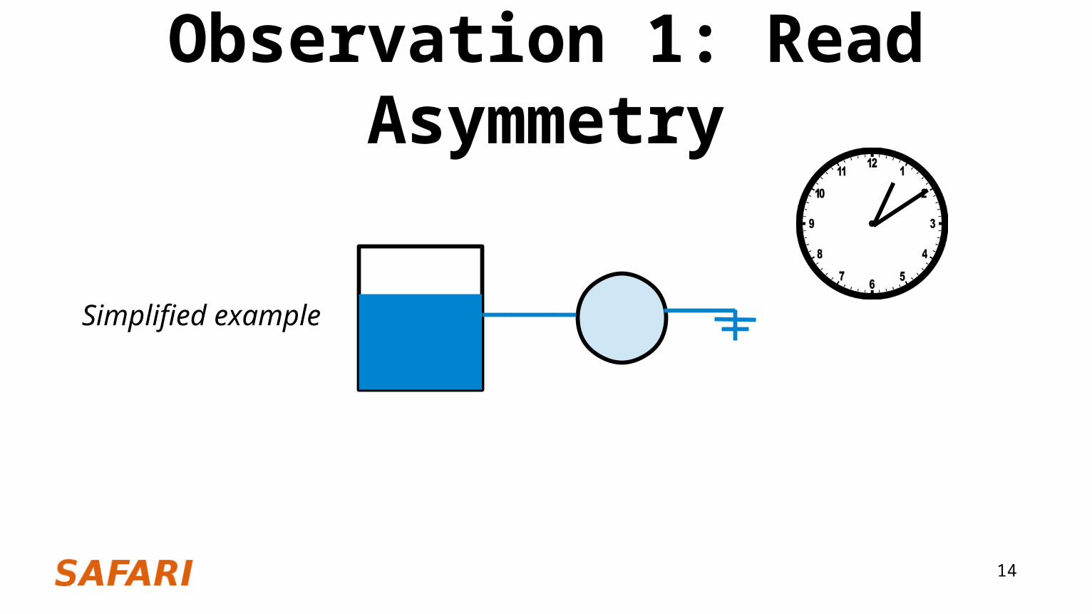
Observation 1: Read Asymmetry
Capacitor filled with reference
voltage
MLC-PCM cell with unknown
resistance
Simplified example
14
Observation 1: Read Asymmetry
Simplified example

15
Observation 1: Read Asymmetry
Simplified example Infer data value
16
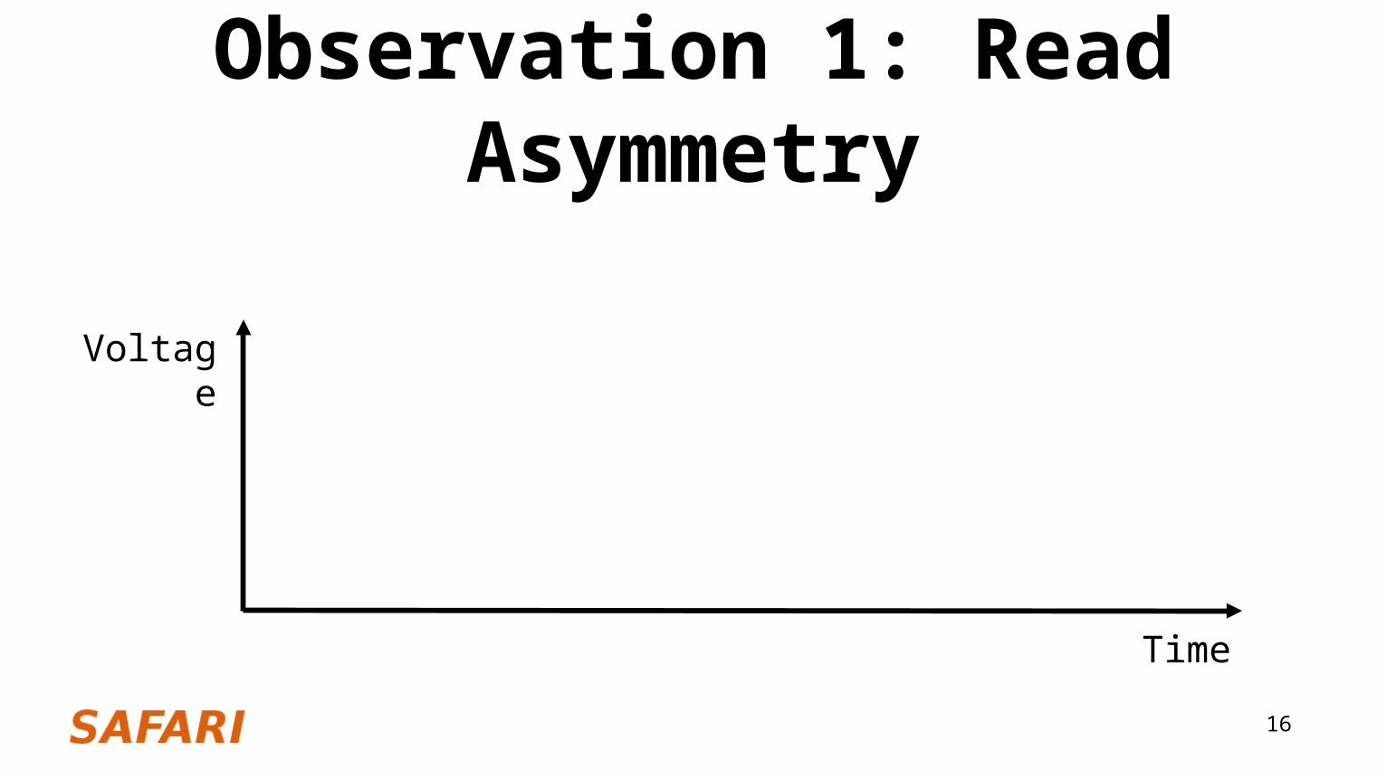
Observation 1: Read Asymmetry
Voltage
Time
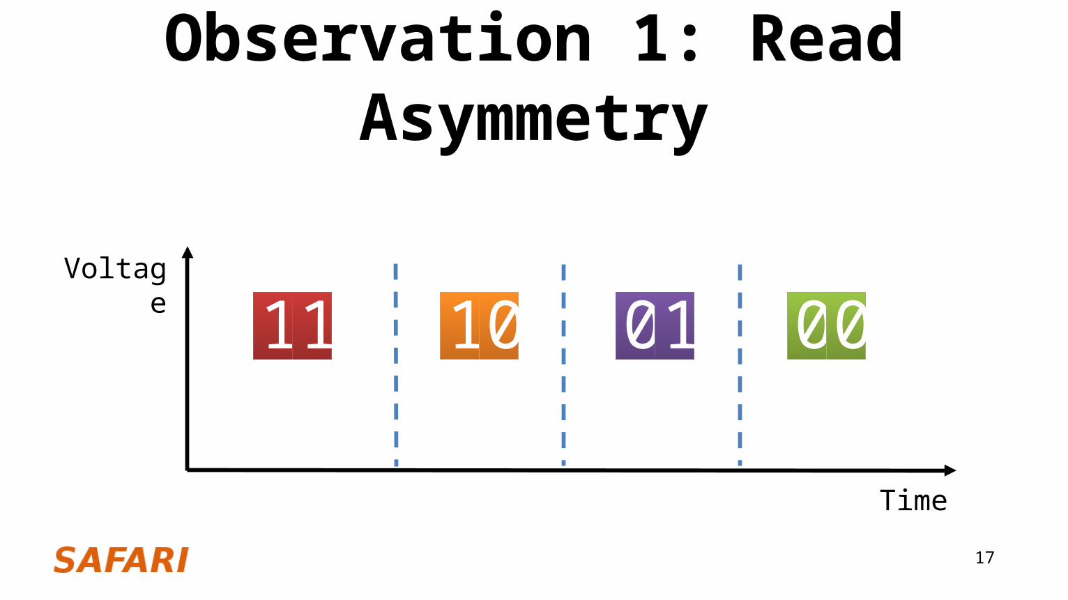
17
Observation 1: Read Asymmetry
Voltage
Time
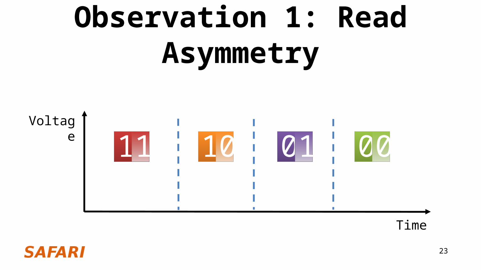
11 000110
18
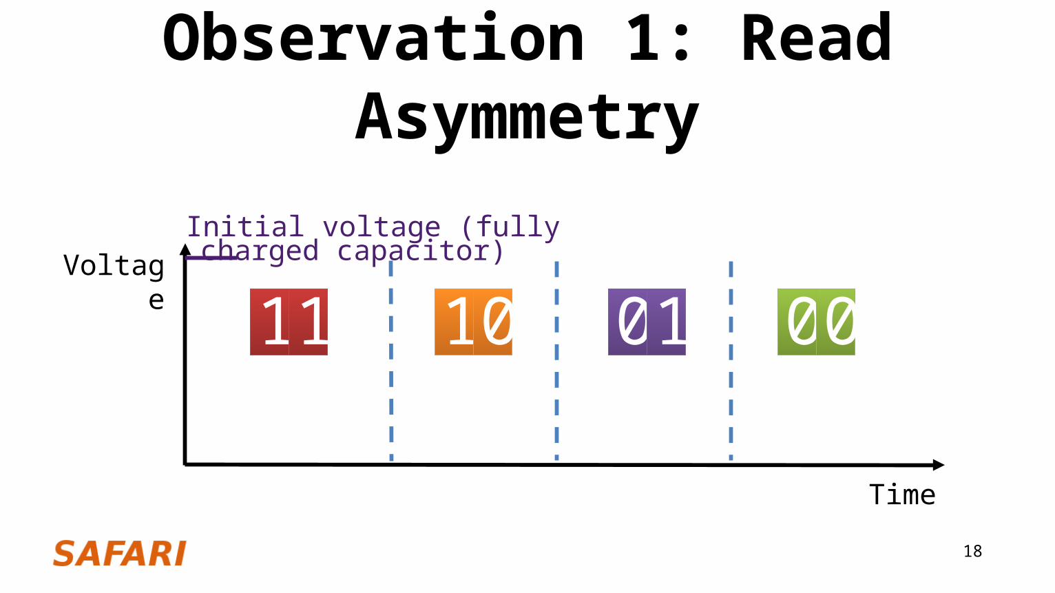
Observation 1: Read Asymmetry
Voltage
Time
Initial voltage (fully charged capacitor)
11 000110
19
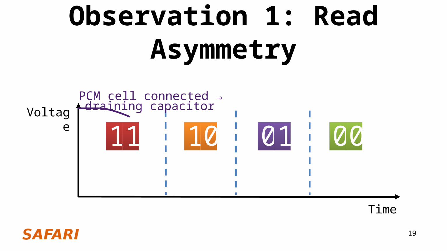
Observation 1: Read Asymmetry
Voltage
Time
PCM cell connected → draining capacitor
11 000110
20
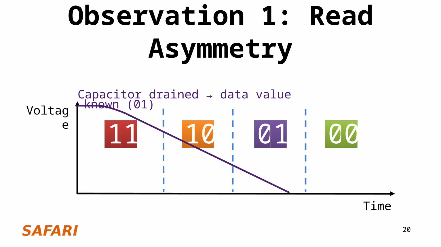
10
Observation 1: Read Asymmetry
Voltage
Time
Capacitor drained → data value known (01)
11 0001
21
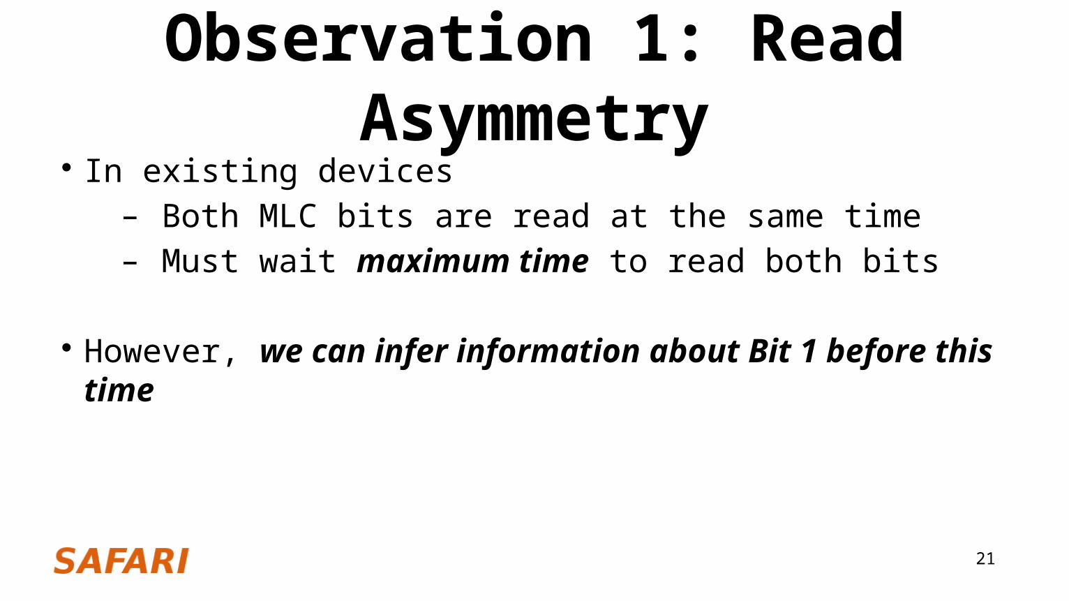
Observation 1: Read Asymmetry In existing devices
– Both MLC bits are read at the same time– Must wait maximum time to read both bits
However, we can infer information about Bit 1 before this time

22
Observation 1: Read Asymmetry
Voltage
Time
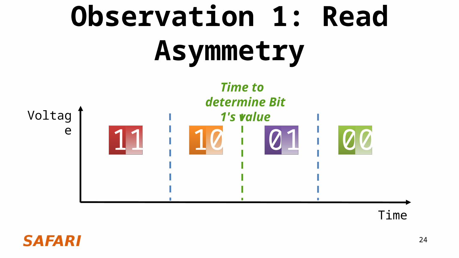
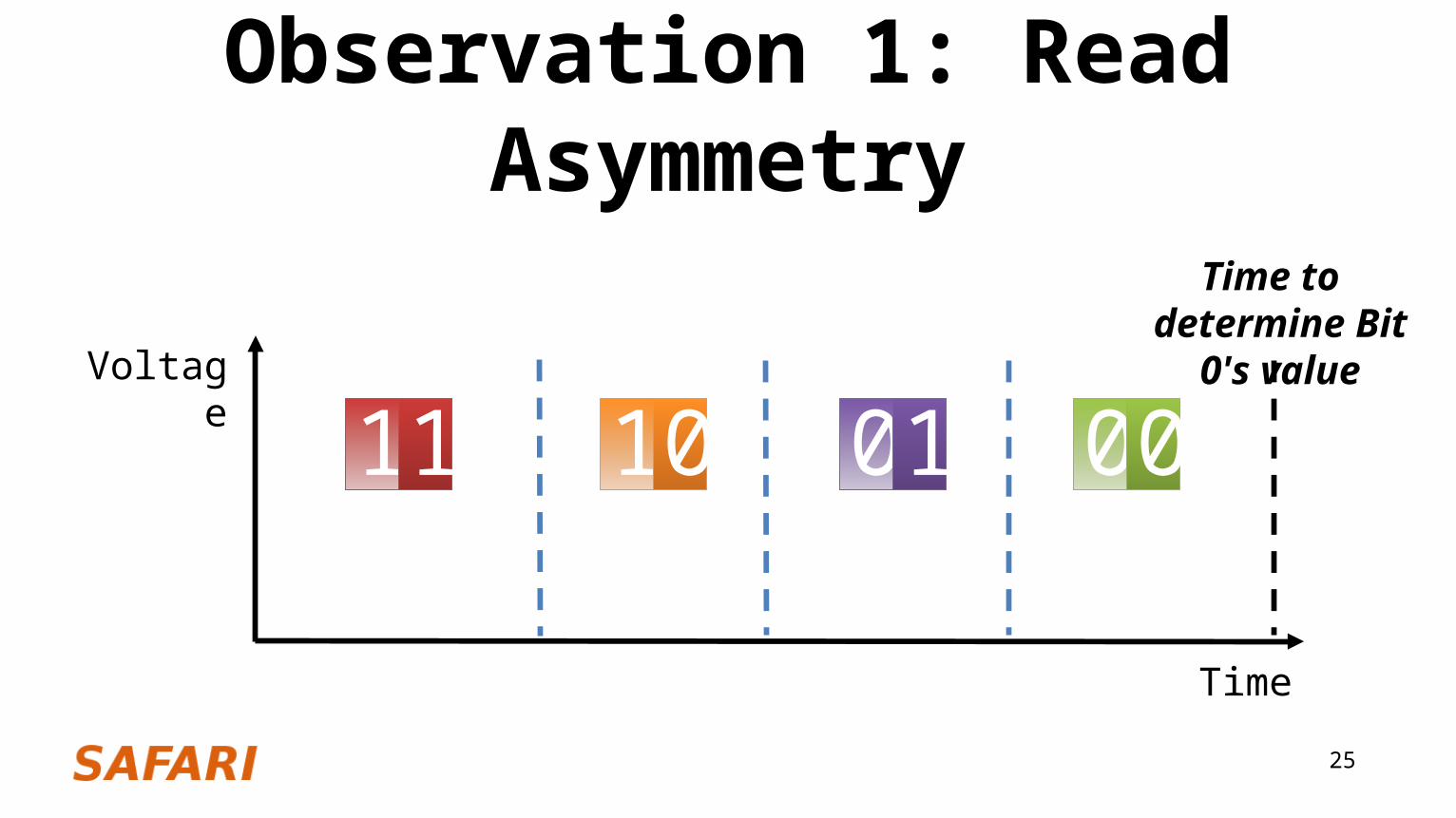
11 000110
23
Observation 1: Read Asymmetry
Voltage
Time
11 000110
24
Observation 1: Read Asymmetry
Voltage
Time
11 000110
Time to determine Bit 1's value
25
Observation 1: Read Asymmetry
Voltage
Time
11 000110
Time to determine Bit 0's value
26
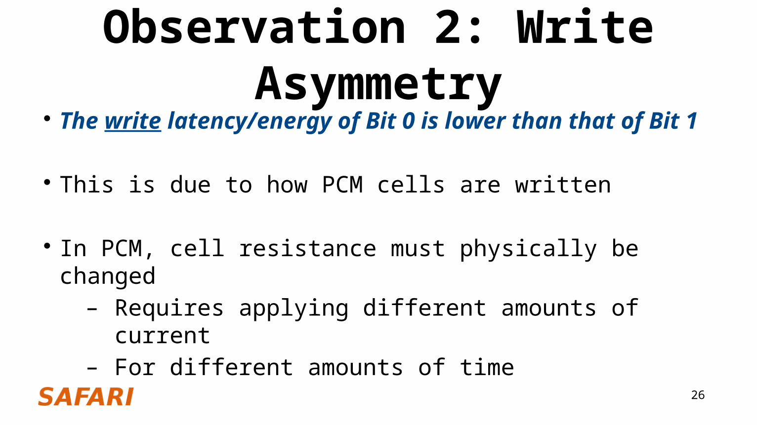
Observation 2: Write Asymmetry The write latency/energy of Bit 0 is lower than that of Bit 1
This is due to how PCM cells are written
In PCM, cell resistance must physically be changed– Requires applying different amounts of current– For different amounts of time
27
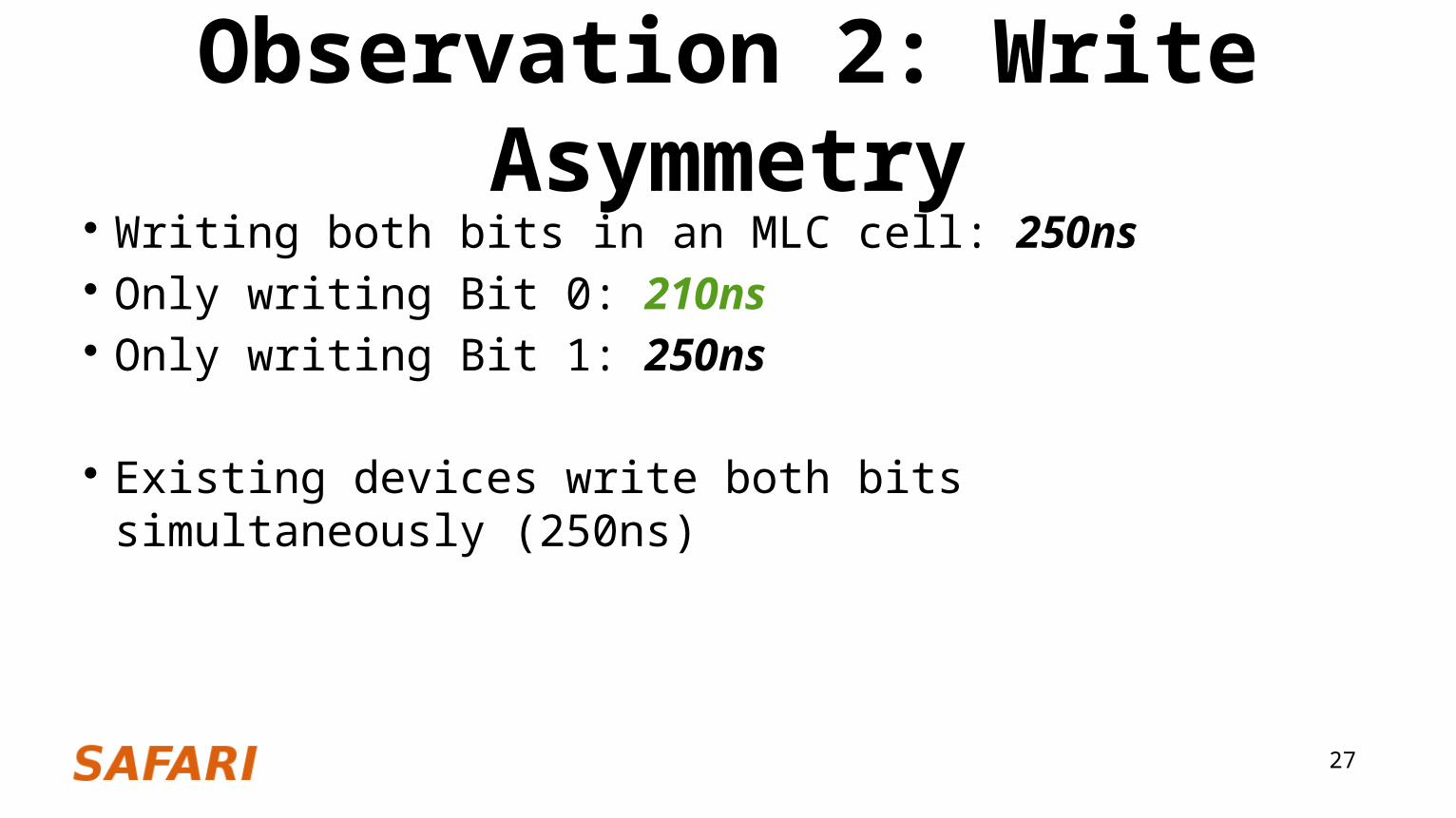
Observation 2: Write Asymmetry Writing both bits in an MLC cell: 250ns Only writing Bit 0: 210ns Only writing Bit 1: 250ns
Existing devices write both bits simultaneously (250ns)
28
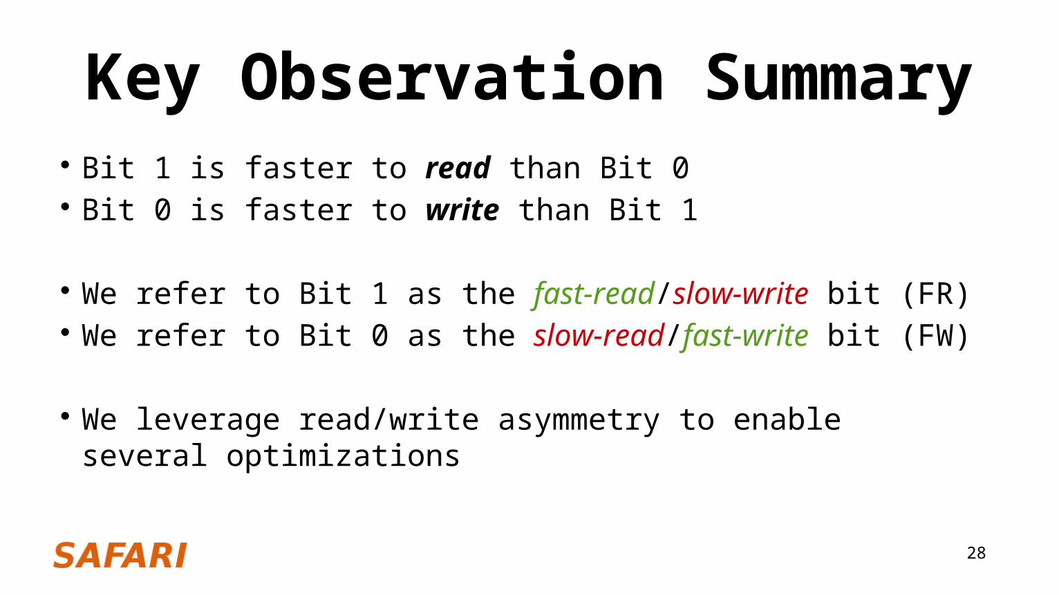
Key Observation Summary Bit 1 is faster to read than Bit 0 Bit 0 is faster to write than Bit 1
We refer to Bit 1 as the fast-read/slow-write bit (FR) We refer to Bit 0 as the slow-read/fast-write bit (FW)
We leverage read/write asymmetry to enable several optimizations
29
Outline Background Problem and Goal Key Observations
– MLC-PCM cell read asymmetry– MLC-PCM cell write asymmetry
Our Techniques– Decoupled Bit Mapping (DBM)– Asymmetric Page Mapping (APM)– Split Row Buffering (SRB)
Results Conclusions
30
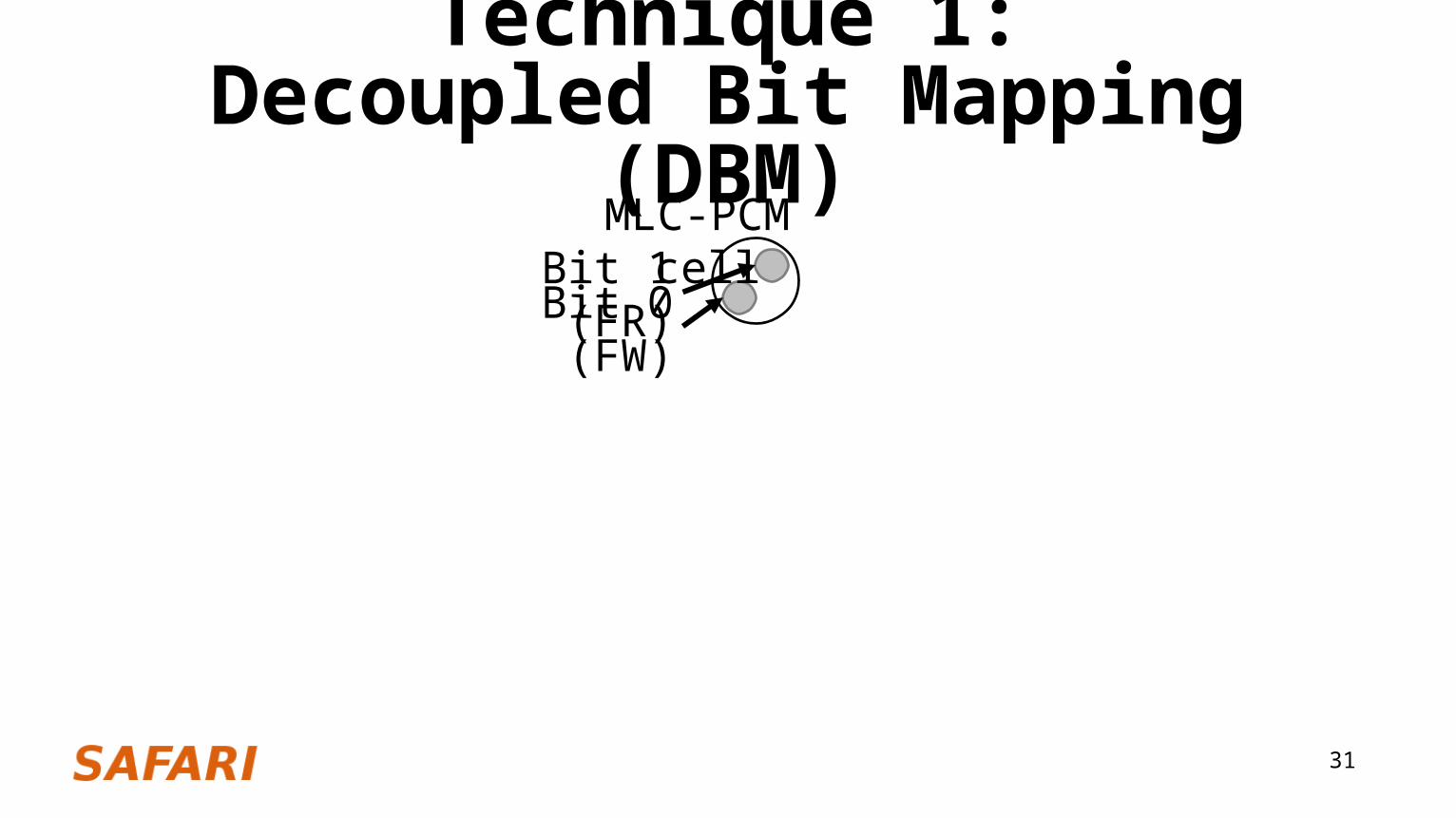
Technique 1:Decoupled Bit Mapping (DBM)
Key Idea: Logically decouple FR bits from FW bits– Expose FR bits as low-read-latency regions of memory– Expose FW bits as low-write-latency regions of memory
31
Technique 1:Decoupled Bit Mapping (DBM)
MLC-PCM cellBit 1 (FR)
Bit 0 (FW)
32
Technique 1:Decoupled Bit Mapping (DBM)
bit
bit
bit
bit
bit
bit
bit
bit
bit
bit
bit
bit
bit
bit
bit
bit
01
23
45
67
89
1011
1213
1415
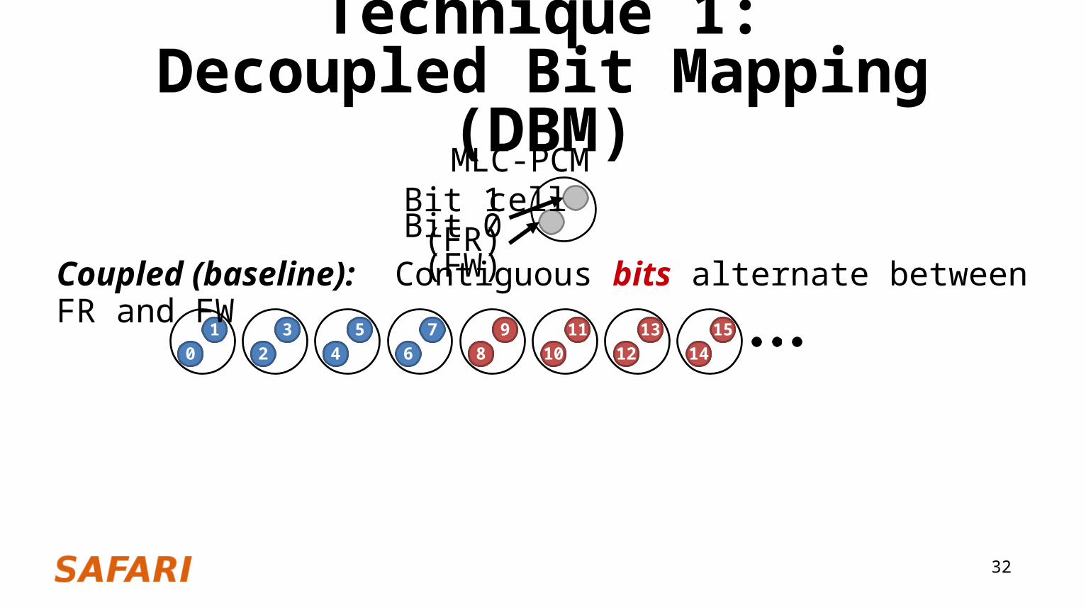
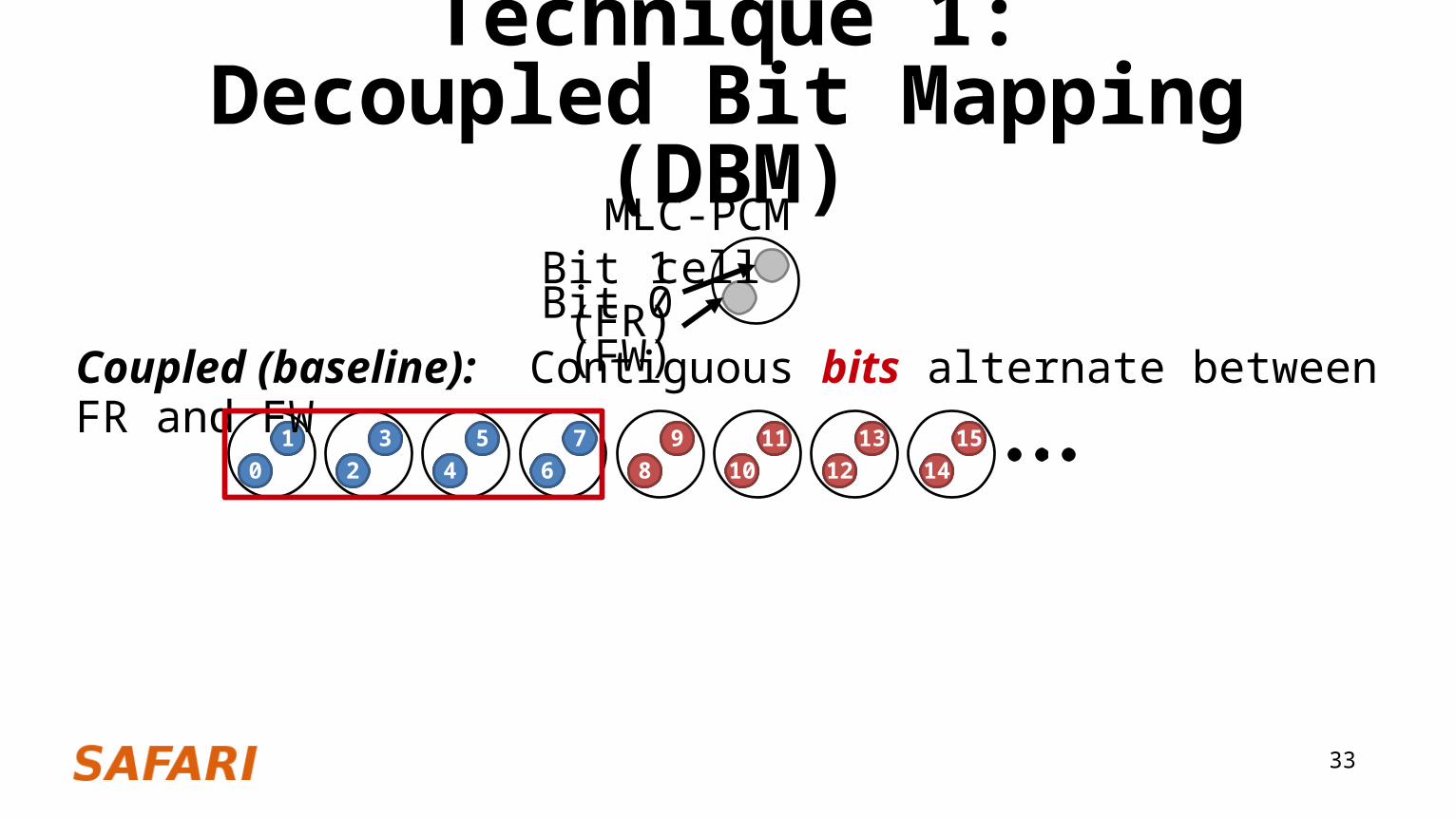
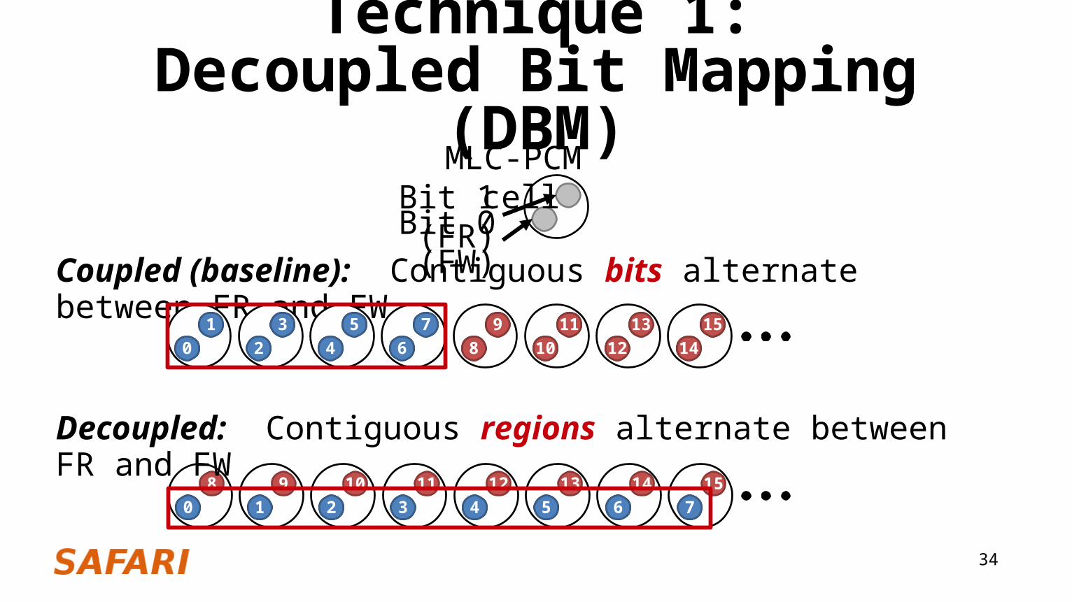
Coupled (baseline): Contiguous bits alternate between FR and FW
MLC-PCM cellBit 1 (FR)
Bit 0 (FW)
33
Technique 1:Decoupled Bit Mapping (DBM)
bit
bit
bit
bit
bit
bit
bit
bit
bit
bit
bit
bit
bit
bit
bit
bit
01
23
45
67
89
1011
1213
1415
Coupled (baseline): Contiguous bits alternate between FR and FW
MLC-PCM cellBit 1 (FR)
Bit 0 (FW)
34
12 13 14 158 9 10 11
Technique 1:Decoupled Bit Mapping (DBM)
bit bit bit bit bit bit bit bit0 1 2 3 4 5 6 7
Coupled (baseline): Contiguous bits alternate between FR and FW
bit
bit
bit
bit
bit
bit
bit
bit
bit
bit
bit
bit
bit
bit
bit
bit
01
23
45
67
89
1011
1213
1415
Decoupled: Contiguous regions alternate between FR and FW
MLC-PCM cellBit 1 (FR)
Bit 0 (FW)
35
Technique 1:Decoupled Bit Mapping (DBM)
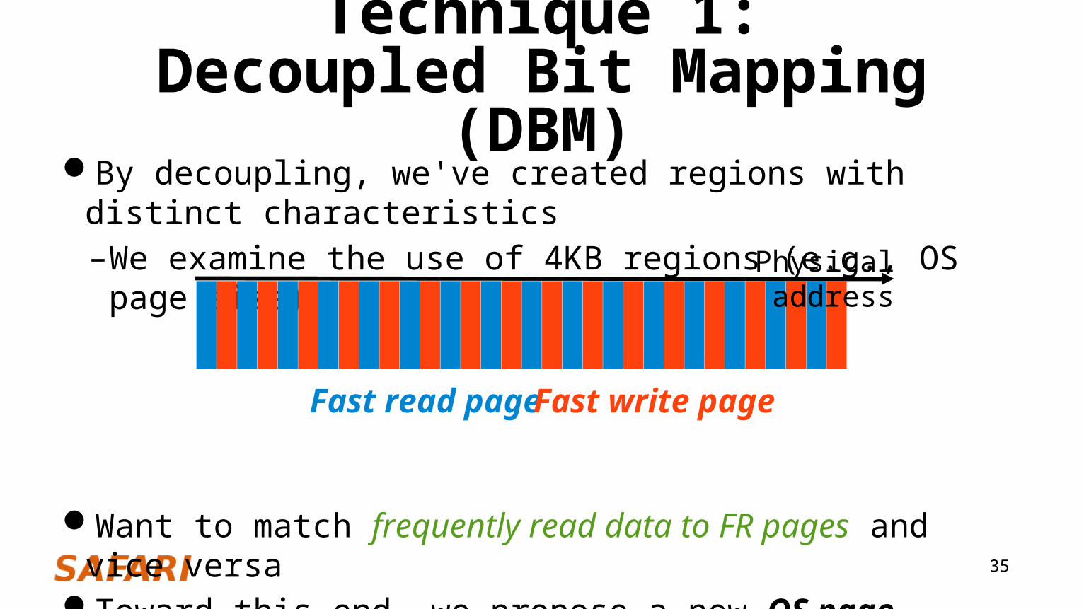
By decoupling, we've created regions with distinct characteristics– We examine the use of 4KB regions (e.g., OS page size)
Want to match frequently read data to FR pages and vice versaToward this end, we propose a new OS page allocation scheme
Fast read page Fast write page
Physical address

36
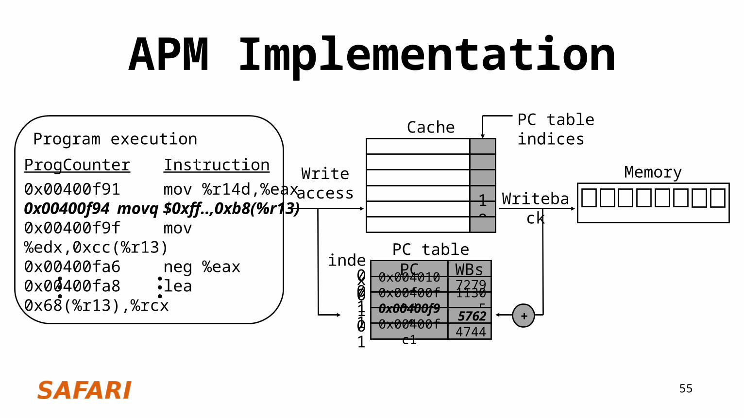
Technique 2:Asymmetric Page Mapping (APM)
Key Idea: predict page read/write intensity and map accordingly– Measure write intensity of instructions that access data– If instruction has high write intensity and first touches page
»OS allocates FW page, otherwise, allocates FR pageImplementation (full details in paper)
– Small hardware cache of instructions that often write data– Updated by cache controller when data written to memory– New instruction for OS to query table for prediction
37
Technique 3:Split Row Buffering (SRB)
Row buffer stores contents of currently-accessed data– Used to buffer data when sending/receiving across I/O ports
Key Idea: With DBM, buffer FR bits independently from FW bits– Coupled (baseline): must use large monolithic row buffer (8KB)– DBM: can use two smaller associative row buffers (2x4KB)– Can improve row buffer locality, reducing latency and energy
Implementation (full details in paper)– No additional SRAM buffer storage– Requires multiplexer logic for selecting FR/FW buffers
38
Outline Background Problem and Goal Key Observations
– MLC-PCM cell read asymmetry– MLC-PCM cell write asymmetry
Our Techniques– Decoupled Bit Mapping (DBM)– Asymmetric Page Mapping (APM)– Split Row Buffering (SRB)
Results Conclusions

39
Evaluation MethodologyCycle-level x86 CPU-memory simulator
– CPU: 8 cores, 32KB private L1/512KB private L2 per core– Shared L3: 16MB on-chip eDRAM– Memory: MLC-PCM, dual channel DDR3 1066MT/s, 2 ranks
Workloads– SPEC CPU2006, NASA parallel benchmarks, GraphLab
Performance metrics– Multi-programmed (SPEC): weighted speedup– Multi-threaded (NPB, GraphLab): execution time
40
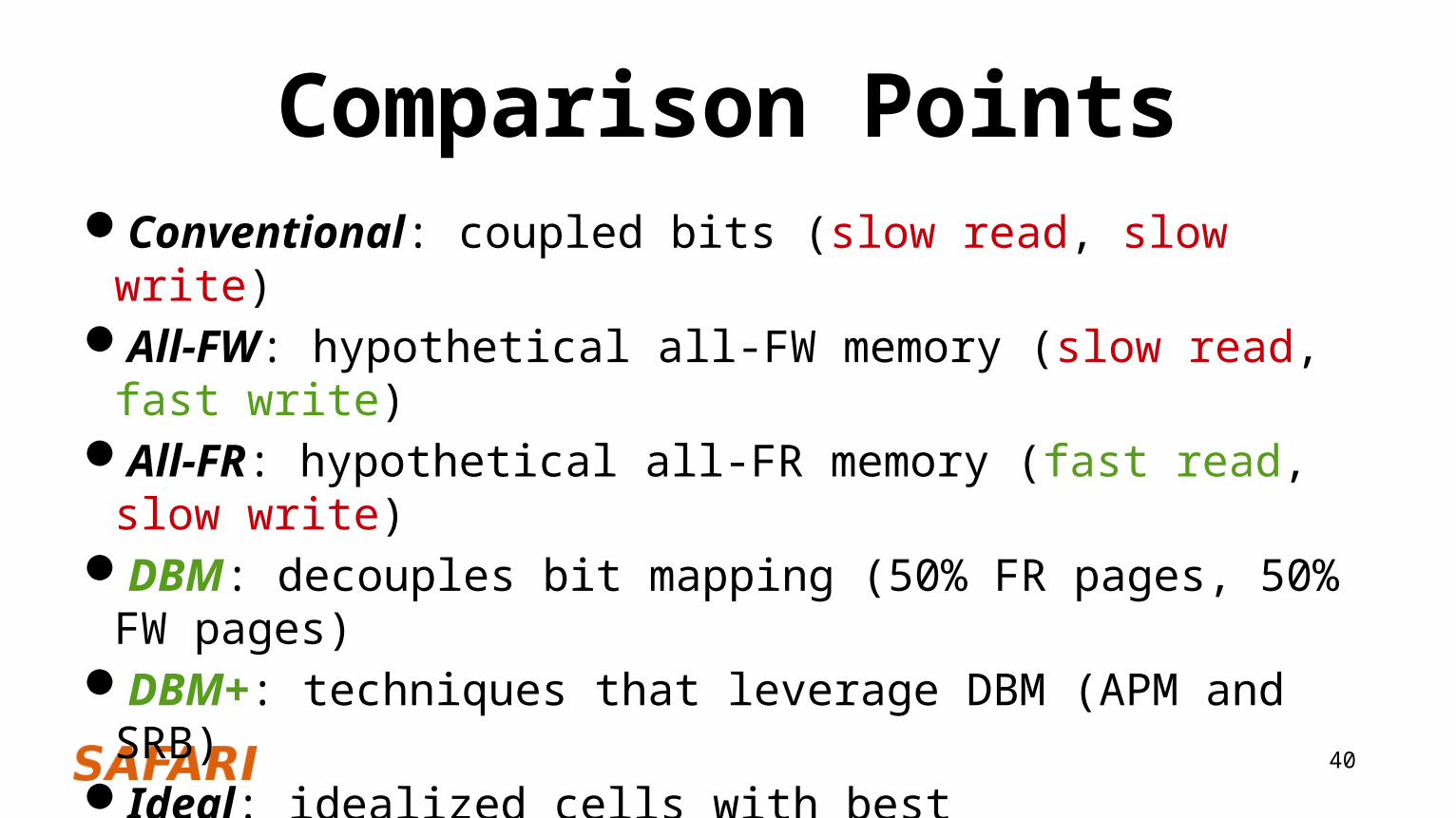
Comparison PointsConventional: coupled bits (slow read, slow write)All-FW: hypothetical all-FW memory (slow read, fast write)All-FR: hypothetical all-FR memory (fast read, slow write)DBM: decouples bit mapping (50% FR pages, 50% FW pages)DBM+: techniques that leverage DBM (APM and SRB)Ideal: idealized cells with best characteristics (fast read, fast write)
41
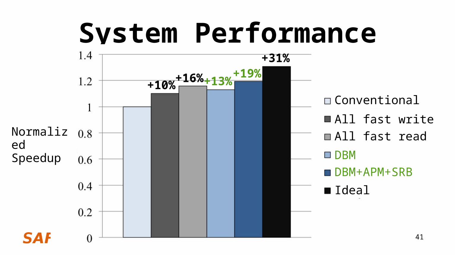
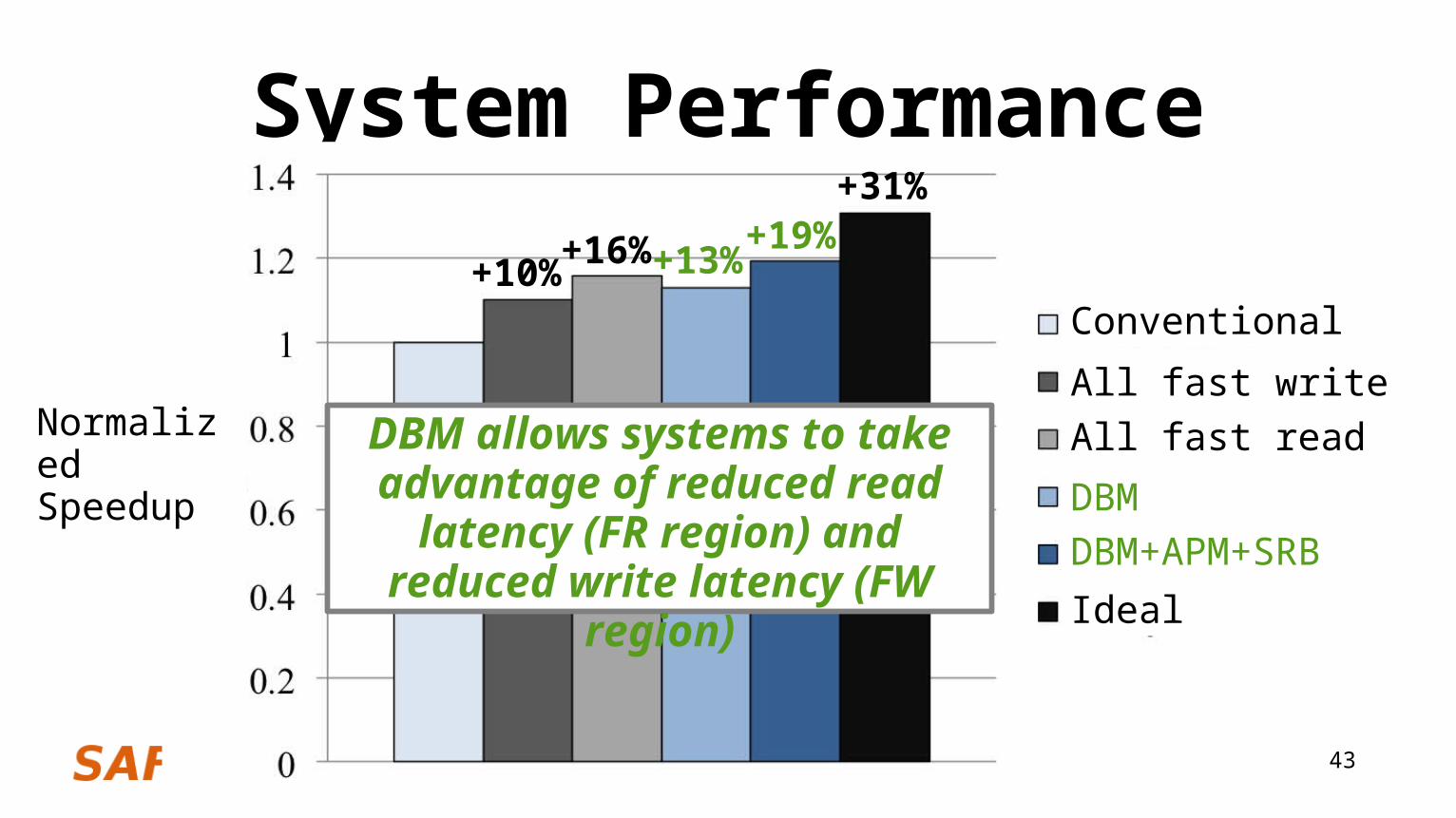
System Performance+19%
+10% +16% +13%
+31%
Conventional
All fast writeAll fast read
DBM DBM+APM+SRB
Ideal
Normalized Speedup

42
System Performance+19%
+10% +16% +13%
+31%
Conventional
All fast writeAll fast read
DBM DBM+APM+SRB
Ideal
All-FR > All-FW → dependent on workload access patterns
Normalized Speedup
43
System Performance+19%
+10% +16% +13%
+31%
Conventional
All fast writeAll fast read
DBM DBM+APM+SRB
Ideal
DBM allows systems to take advantage of reduced read latency
(FR region) and reduced write latency (FW region)
Normalized Speedup

44
Memory Energy Efficiency+14%
+5%+12% +8%
+30%
Conventional
All fast writeAll fast read
DBM DBM+APM+SRB
Ideal
Normalized Performance per Watt

45
Memory Energy Efficiency+14%
+5%+12% +8%
+30%
Conventional
All fast writeAll fast read
DBM DBM+APM+SRB
Ideal
Benefits from lower read energy by exploiting read
asymmetry (dominant case) and from lower write energy by
exploiting write asymmetry
Normalized Performance per Watt
46
Other Results in the PaperImproved thread fairness (less resource contention)
– From speeding up per-thread execution
Techniques do not exacerbate PCM wearout problem– ~6 year operational lifetime possible
47
Outline Background Problem and Goal Key Observations
– MLC-PCM cell read asymmetry– MLC-PCM cell write asymmetry
Our Techniques– Decoupled Bit Mapping (DBM)– Asymmetric Page Mapping (APM)– Split Row Buffering (SRB)
Results Conclusions
48
Conclusions Phase-change memory (PCM) is a promising emerging technology
More scalable than DRAM, faster than flash Multi-level cell (MLC) PCM = multiple bits per cell → high density
Problem: Higher latency/energy compared to non-MLC PCM Observation: MLC bits have asymmetric read/write characteristics
Some bits can be read quickly but written slowly and vice versa
49
Conclusions Goal: Read data from fast-read bits; write data to fast-write bits Solution:
Decouple bits to expose fast-read/write memory regions Map read/write-intensive data to appropriate memory regions Split device row buffers to leverage decoupling for better locality
Result:– Improved performance (+19.2%) and energy efficiency (+14.4%)– Across SPEC CPU2006 and data-intensive/cloud workloads

50
Thank You!

Efficient Data Mapping and Buffering Techniques for Multi-
Level Cell Phase-Change MemoriesHanBin Yoon, Justin Meza,
Naveen Muralimanohar*, Onur Mutlu, Norm Jouppi*†
Carnegie Mellon University * Hewlett-Packard Labs † Google, Inc.

52
Backup Slides
53
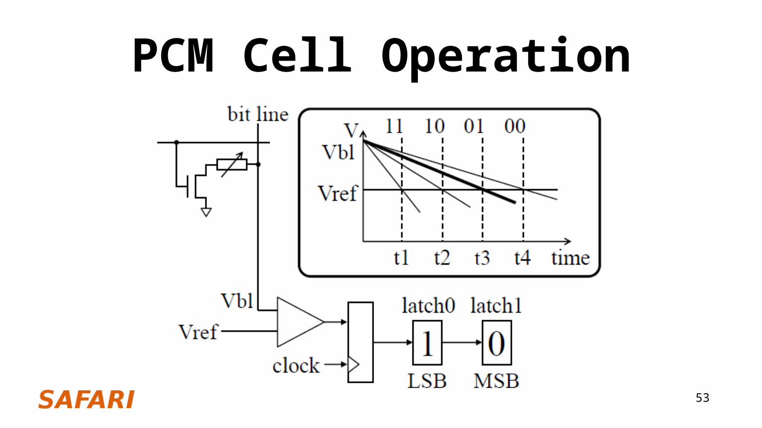
PCM Cell Operation

54
Integrating ADC
55
APM Implementation
ProgCounter Instruction
Cache
Write access Writeback
Memory
PC WBs0x0040100f 72790x00400fbd 113050x00400f94 57620x00400fc1 4744
PC table
+
0x00400f91 mov %r14d,%eax0x00400f94 movq $0xff..,0xb8(%r13)0x00400f9f mov %edx,0xcc(%r13)0x00400fa6 neg %eax0x00400fa8 lea 0x68(%r13),%rcx
00011011
10
Program execution .PC table indices
index


![[B. mutlu sumer,_jorgen_fredsoe]_hydrodynamics_aro(book_fi.org)](https://img.pdfslide.us/doc/110x75/55557f05b4c9055f5f8b5100/b-mutlu-sumerjorgenfredsoehydrodynamicsarobookfiorg.jpg)