Embed Size (px)
Citation preview

Efficient Algorithm and Architecture for Implementation of Multiplier Circuits in Modern FPGAs
Jacques Laurent Athovv
Department of Electrical and Computer Engineering
Presented in Partial Fulfillment of the Requirements for
Degree of Master of Applied Science
Concordia University, Montreal, Canada
November 2008
© Jacques L Athow, 2008

1*1 Library and Archives Canada
Published Heritage Branch
395 Wellington Street Ottawa ON K1A 0N4 Canada
Bibliotheque et Archives Canada
Direction du Patrimoine de I'edition
395, rue Wellington OttawaONK1A0N4 Canada
Your file Votre reference ISBN: 978-0-494-63306-9 Our file Notre reference ISBN: 978-0-494-63306-9
NOTICE: AVIS:
The author has granted a nonexclusive license allowing Library and Archives Canada to reproduce, publish, archive, preserve, conserve, communicate to the public by telecommunication or on the Internet, loan, distribute and sell theses worldwide, for commercial or noncommercial purposes, in microform, paper, electronic and/or any other formats.
L'auteur a accorde une licence non exclusive permettant a la Bibliotheque et Archives Canada de reproduce, publier, archiver, sauvegarder, conserver, transmettre au public par telecommunication ou par I'lnternet, preter, distribuer et vendre des theses partout dans le monde, a des fins commerciales ou autres, sur support microforme, papier, electronique et/ou autres formats.
The author retains copyright ownership and moral rights in this thesis. Neither the thesis nor substantial extracts from it may be printed or otherwise reproduced without the author's permission.
L'auteur conserve la propriete du droit d'auteur et des droits moraux qui protege cette these. Ni la these ni des extraits substantiels de celle-ci ne doivent etre imprimes ou autrement reproduits sans son autorisation.
In compliance with the Canadian Privacy Act some supporting forms may have been removed from this thesis.
Conformement a la loi canadienne sur la protection de la vie privee, quelques formulaires secondaires ont ete enleves de cette these.
While these forms may be included in the document page count, their removal does not represent any loss of content from the thesis.
Bien que ces formulaires aient inclus dans la pagination, il n'y aura aucun contenu manquant.
• + •
Canada

ii

HI
ABSTRACT
Efficient Algorithm and Architecture for Implementation of Multiplier Circuits in Modern FPGAs
Jacques L Athow
High speed multiplication in Field Programmable Gate Arrays is often performed
either using logic cells or with built-in DSP blocks. The latter provides the highest
performance for arithmetic operations while being also optimized in terms of power
and area utilization. Scalability of input operands is limited to that of a single DSP
block and the current CAD tools provide little help when the designer needs to build
larger arithmetic blocks. The present thesis proposes an effective approach to the
problem of building large integer multipliers out of smaller ones by giving two
algorithms to the system designer, for a given FPGA technology. Large word length is
required in applications such as cryptography and video processing. The first proposed
algorithm partitions large input multipliers into an architecture-aware design. The
second algorithm then places the generated design in an optimal layout minimizing
interconnect delay. The thesis concludes with simulation and hardware generated data
to support the proposed algorithms.

IV
ACKNOWLEDGEMENTS
I would like to take the opportunity and thank everyone that made my research
possible, which culminated with this thesis. In particular, I am indebted to my
professor Asim who always encouraged me. He guided me during my thesis with his
useful insight in the field of FPGAs and low level interconnects. He would always
make me think out-of-the-box with his no-nonsense approach. To my many professors
that I had throughout my stay at Concordia University including Professors Tahar,
Amer, Lam, the late Gohary and Ted Obuchowicz, without whom I would never have
known the world of VHDL. Indirectly to Peter Alfke and Ray Andraka for their work
and guidance on the FPGA Usenet forum. To the staff at the AITS helpdesk and the
librarians at the Webster library. Finally, to my parents who initially made everything
possible and were always there to provide moral support.

V
TABLE OF CONTENTS
LIST OF FIGURES ix
LIST OF TABLES xii
1. INTRODUCTION 1
1. 1 Contribution 3
1. 2 Thesis Organization 4
2 Field Programmable Gate Arrays 5
2. 1 Basic Multiplication 8
3 FPGA Multiplication Algorithms 10
3. 1 Serial-Parallel Signed Multiplier 10
3. 2 Carry Save Array Multiplier 11
3. 3 Constant Coefficient Multiplier 12
3. 4 Partial Product Look-Up Table Multiplier 13
3. 5 Partition Multiplication Algorithm (Shuli-Gao et al) 14
3. 6 Summary of Multiplication Algorithms 21
4 Xilinx Virtex Family FPGA 22
4. 1 Logic Cells 23
4. 2 Virtex Hardware Arithmetic 25
4.3 Xilinx DSP48 Arithmetic Block 27
4. 4 Interconnect 31
4. 5 Congestion 33
4. 6 Summary of Techniques 33
5 Partition Algorithm for Virtex-4 FPGA 35
5. 1 Details of Operation 36

vi
5. 2 Arithmetic Cell A Block 39
5. 3 Arithmetic Cell B Block and Cascade Register 40
5. 4 Partition Algorithm Description 41
5. 5 Resources Utilization 44
5. 6 Performance Equations 44
5. 7 Non-Pipeline Design 45
5.8 Results 48
5.8.1 Combinational path delay 49
5.8.2 Virtex-4 logic slice utilization 50
5.8.3 Virtex-4 DSP48 slice usage 51
5.8.4 Area delay (AT2) product 52
5.8.5 Power dissipation 53
5.8.6 Other results 54
5. 9 Summary 56
6 Placement algorithm for large-unsigned multipliers 57
6. 1 Introduction 57
6. 2 Placement Problem Formulation 59
6. 3 Related Work on Placement Algorithms 61
6.3.1 Placement algorithms for FPGA 61
6.3.2 Heterogeneous Floorplanner for FPGA 63
6.3.3 HPLAN Heterogeneous Floorplanner 63
6.3.4 HPLAN problem formulation 64
6.3.5 Comments 66
6. 4 Relative Placement Macros 67
6. 5 Area, delay and Power Heuristics 69

vii
6.5.1 Area 69
6.5.2 Delay 70
6.5.3 Power 70
6. 6 Proposed Placement Algorithm 71
6.6.1 Area constraints formulation 72
6.6.2 Congestion Factor 74
6.6.3 Objective function 75
6.6.4 Graph theory 75
6. 7 Proposed Placement Algorithm 76
6.8 Results 79
6.8.1 Combinational path delay 80
6.8.2 Virtex-4 logic slice utilization for placed design 81
6.8.3 Place-and-route tool runtime 82
6. 9 Summary 83
7 Testing strategy 84
7. 1 Behavioural Testing 85
7. 2 Timing Analysis 86
7. 3 Placement Algorithm Testing 86
8 Conclusion and future work 87
8. 1 Partition Algorithm 87
8. 2 Placement Algorithm 87
8. 3 Conclusion 88
8.4 Future Work 89
REFERENCES 90
APPENDIX A, VHDL MODELS 93

Vl l l
APPENDIX B, C++ SOURCE CODE 110

ix
LIST OF FIGURES
Figure 2.1 Current FPGA technologies and trend towards built-in DSP blocks 6
Figure 2.2 Virtex Family FPGA with amount of DSP blocks 7
Figure 3.1 Serial Parallel N-bit multiplier architecture 11
Figure 3.2 Carry Save Array multiplier architecture 12
Figure 3.3 N-bit constant coefficient unsigned multiplier 13
Figure 3.4 Architecture for Partial-Product Look-up Multiplier using 6bits LUT.... 14
Figure 3.5 Long-Integer Multiplication Decomposition according to [4] 16
Figure 3.6 Sequence of addition operation for algorithm [4] when m is even and odd
19
Figure 3.7 Graph of gate and interconnect (wire) delay versus technology for Virtex
FPGA for a 16x2bit unsigned multiplier 21
Figure 4.1 Trend for Xilinx FPGA during past 16 years 23
Figure 4.2 Xilinx FPGA logic cell evolution during past 15 years 25
Figure 4.3 Hardware dedicated for arithmetic operations in Virtex FPGA 26
Figure 4.4 Internal view of Virtex-4 DSP48 tile (block) [15] 28
Figure 4.5 DSP48 slice to CLB area ratio, as shown in Xilinx FPGAEDITOR 28
Figure 4.6 Different interconnect classes found in the Virtex family of FPGA [19]. 32
Figure 5.1 Technology mapping of [4] into proposed architecture for a 68bits
unsigned multiplier 37
Figure 5.2 DSP48 tile internal configuration 38
Figure 5.3 Internal view of Arithmetic Cell A block 40
Figure 5.4 Internal view of Arithmetic Cell B block 41
Figure 5.5 Internal view of Cascade Register block 41

X
Figure 5.6 Long-integer 68x68bit multiplier generated by proposed algorithm 43
Figure 5.7 Area-Delay product for non-pipeline multipliers 47
Figure 5.8 Combinational path delay for different sized inputs 49
Figure 5.9 Amount of Virtex-4 slices used against different sized inputs 50
Figure 5.10 Number of DSP48 slices against different sized inputs 51
Figure 5.11 Area Delay product (AT2) performance measure 52
Figure 5.12 Power dissipation for different sized inputs 53
Figure 5.13 Routing performance degradation for higher word length 54
Figure 5.14 Layout of placed 136xl36bit multiplier circuit inside a Virtex-4 FX140
FPGA 55
Figure 6.1 Design using proposed set of algorithm 59
Figure 6.2 Example of floorplan generated using HPLAN 64
Figure 6.3 Usage of Relative Location in hardware descriptive language 67
Figure 6.4 Internal logic slice arrangement using RLOC attribute 68
Figure 6.4 Hierarchy representation using HSET and HU_SET 69
Figure 6.5 ACA, ACB, CR Macro blocks internal placement 72
Figure 6.6 Macro blocks physical dimensions 74
Figure 6.7 51Bit Multiplier graph 76
Figure 6.8 51Bit multiplier physical layout graph, as generated by proposed partition
algorithm 79
Figure 6.9 Combinational path delay for designs initially placed using proposed
placement algorithm 80
Figure 6.10 Interconnect delay in placed multiplier designs 81
Figure 6.11 Logic slice utilization for placed multipliers designs 82
Figure 6.12 Place-and-route run-time for different multiplier designs 83
xi
Figure 7.1 Testing hierarchy for multiplier partition algorithm 84
Figure 7.2 Test setup for multiplier designs 85

xii
LIST OF TABLES
Table 1.1 Performance of HDL, Coregen, Algorithm [1] and Proposed Algorithm. ..2
Table 4.1 Valid opmode for dsp48 block, with respect to z multiplexer [18] 29
Table 4.2 Valid opmode for dsp48 block, with respect to x and y multiplexer [19]. 30
Table 4.3 Carryinsel control bits with corresponding opmode operation [20] 30
Table 5.1 OPMODE/CARRY configuration bits for SliceO and Slicel 39
Table 5.2 Performance results for combinational delay, non-pipelined designs 46
Table 5.3 Performance results for area utilization, non-pipelined designs 47

1
1. INTRODUCTION
Binary multiplication operations are at the center of many system level blocks
used in high performance applications. The efficiency of the operation is crucial in
order to have an edge over the competition. As an example, one of the latest television
standard developed, the high-definition television (HDTV) is based on the MPEG-2
compression algorithm [1]. This works at a lower level with Discrete Cosine
Transforms (DCT) and Inverse DCTs which are bottom-line Fast Fourier Transform
(FFT) operations [2]. The performance of FFT [3] is measured by the number of
multiplication and addition operations per second. The higher the number, the higher
the amount of frame compressed in unit time, hence a better quality. An HD-DVD
recorder built around an efficient MPEG compression unit will generally perform
better than one made up of conventional system blocks. Other applications of long
integer multipliers include cryptography and hardware accelerator for software
mathematic packages and algorithms.
Presently there is a lack of Computer Aided Design (CAD) tools available to the
system designer, which solve the problem of creating high-performing long-word
multiplier circuits in Field Programmable Gate Array chips (FPGA). Current solutions
include using the multiplication operator in Hardware Descriptive Languages (HDL)
or using CAD applications such as Xilinx COREGenerator, to generate pre-built
netlist files. Both solutions have limitations; using the VHDL multiplication operator
will request from the HDL synthesizer the corresponding netlist. In most cases, the
generated multiplier will not be based on high performance arithmetic blocks

2
available in the FPGA or will be un-pipelined. The current COREGenerator software
has limitation in terms of size of input operands allowed and is constrained to a
maximum of 64bits. The following table summarizes the performance of various
methodologies available to implement unsigned multipliers.
TABLE 1.1 PERFORMANCE OF HDL, COREOEN, ALGORITHM [4] AND PROPOSED ALGORITHM.
Methodology
Maximum Frequency Pipelining
Maximum Word Width
HDL
MEDIUM
LIMITED
UNLIMITED
CORE Generator
HIGH
OPTIMUM
64 Bits
GENERIC ALGORITHM [4]
HIGH
OPTIMUM
UNLIMITED
PROPOSED ALGORITHM [5]
VERY HIGH
OPTIMUM
UNLIMITED
The focus of this thesis is the implementation of unsigned long-word hardware
multipliers more specifically using Xilinx Field Programmable Gate Array (FPGA)
chips. As shown in Table 1.1, the proposed algorithm improves the generic algorithm
[4] by increasing performance in terms of maximum frequency of operation. The size
of the largest multiplier which can be implemented is limited only by the size of the
FPGA, in terms of logic cells and arithmetic blocks used. The proposed partitioning
algorithm thus increases utilization of high performance Digital Signal Processing
(DSP) blocks available in Xilinx FPGA chips by breaking down long word operands
into small subsets and performing multiplications on them.

3
1.1 Contribution
This thesis presents two algorithms which will help a system designer develop
high performance unsigned long-integer word multiplier using Xilinx Virtex-4 family
of FPGA. The first proposed algorithm [7] shows how to adapt the Virtex-4
architecture, in particular, DSP48 blocks, to the generic partition multiplier algorithm
presented by Shuli Gao et al [4]. A second algorithm [8] further improves solutions
generated by the partition algorithm by addressing the problem of placement
associated with macro cells used by the proposed partition algorithm and results in an
optimal arrangement reducing power, delay or area. The algorithms presented here
have been verified for functionality and increase in performance. Algorithms are
presented as high-level C++ source code.

1. 2 Thesis Organization
4
This thesis is organized as follows. Chapter 2 introduces Field Programmable Gate
Array technology along with a simple multiplication procedure. In Chapter 3,
multiplication algorithms that are optimized for FPGA architectures are presented
while Chapter 4 gives details about the architecture and arithmetic speed-up
techniques available in the Xilinx Virtex FPGA. Chapter 5 elaborates on the proposed
partition algorithm which is the central part of the thesis. Furthermore, Chapter 6
gives a new placement algorithm that solves the problem associated with the
floorplanning of large multiplier circuits in modern FPGA. Chapter 7 demonstrates
how verification was done and how results were obtained. Finally, Chapter 8
concludes the thesis and offers directions for future work.

5
2 FIELD PROGRAMMABLE GATE ARRAYS
FPGA devices provide an ideal platform to design and test digital systems without
the hassle associated with fabrication usually required for gate arrays and Application
Specific Integrated Circuits (ASIC) technologies. For a long time though, FPGAs
were limited to system clocks not exceeding a few hundreds megahertz but today,
with the advent of smaller process technologies, a well pipelined design can go
beyond the 400MHz boundary while arithmetic operations such as multiplication can
easily reach 550MHz on the latest FPGA generation. In order to achieve the half
Gigahertz level, FPGA designers resorted to custom sub-circuits built on the same
FPGA die. These low level blocks are optimized for arithmetic operations (DSP) and
data processing (microprocessor). The algorithm presented in this thesis employs
arithmetic blocks, more precisely Xilinx DSP48, to perform long word multiplication
in hardware.
Initially, an analysis of FPGA technologies was performed with the conclusion
that FPGA manufacturers had started integrating dedicated and highly optimized sub-
circuits into FPGA chips. This trend, which is shown in Figure 2.1, is due to the fact
that smaller process technology allows for a denser FPGA and the list of practical
innovations includes having high performance application-specific blocks on-chip.

6
Figure 2.1 Current FPGA technologies and trend towards built-in DSP blocks
Being on the same hardware support also provides the designer with the most
flexible, performing, cost effective, space and power efficient solution. A
microprocessor built in the FPGA chip would allow an optimal placement of the
support circuitry while incurring the least amount of delay and would not require any
area from the printed circuit board. As for power consumption, the microprocessor
being a standard cell built using the latest process technology would give reasonable
energy utilization. The choice of specialized circuits built in FPGA chips offered by
manufactures includes DSP blocks, high-speed I/O, embedded memory and
microprocessor blocks.
Figure 2.2 shows the trend in DSP technology for the Xilinx Virtex FPGA family
across 4 generations. It clearly indicates that more DSP blocks are provided in the
latest FPGA along with rising functionality and performance. From Figure 2.1, it can
also be said that generally, the inclusion of these DSP blocks is done by most FPGA
manufactures. Thus, it is safe to develop a suitable algorithm to solve the problem of
long-word unsigned integer multiplication.

NUMBER OF DSP BLOCKS ACROSS XILINX FPGA FAMILY
Fmi,=173MHz 18xJ 8 Signed Multiplication
LLliLiJ ,_B_II
^
Fiu;i=219MH2 18x18 Signed Multiplication
FM=500MHz 18x18 Signed Multiplication Built-in 4Sbit Accumulator Pipelined Option
F_*=550MHz 25x18 Signed Multiplication Adder. Subtracter, Accumulator Pipelined Option
. o_aj_LJ_l
&
Figure 2.2 Virtex Family FPGA with amount of DSP blocks

8
2.1 Basic Multiplication
Multiplication is fundamentally based on a sequence of addition operations. We
shall define for the purpose of explanation three positive integer variables: X
(Multiplicand), Y (Multiplier) and Z (Result).
Binary Long Multiplication
101010 x
010
0000000000
0001010100
0000000000
0001010100
One way to achieve multiplication is by iterating Y times the summation of X with
itself, keeping along the way the running sums of previous steps. The time complexity
of such an algorithm is N, meaning that N additions are required before a valid result
is obtained. Another approach is to perform a series of base multiplications and
additions. The latter is less efficient requiring the knowledge of base multiplication and
powers. This is also known as the long multiplication method with time complexity of
n log(«). With the advent of binary computers though, it became easy to implement
long multiplication algorithm in hardware. The performance was also better since
multiplying by the binary base is a left shift operation and the multiplication itself
results in either the operand or zero. Hence the time complexity reduces to only
log(rc) additions. This is an improvement over the iterated addition multiplication.
General Multiplication Using Iterated Summation
Z = XxY Z = 0ifY = 0orX = 0,Z = XifY = l
Z = X + ...X...+X,Ytimes
z = Zx
Decimal Long Multiplication
1234567 x
890
0000000000
0111111030
0987653600
1098764630

9
The proposed partition algorithm is based on the large-integer multiplication
algorithm presented by Shuli Gao et al [4]. Presented here is an extension of the
algorithm with details about an efficient technology mapping using DSP48 blocks.
The placement problem which arises with the proposed partition algorithm is also
solved with a greedy algorithm where area and delay are used as objective functions.

10
3 FPGA MULTIPLICATION ALGORITHMS
Different techniques for integer multiplication in FPGA exist in literature. We will
investigate only those that are required for a good understanding of the proposed
algorithm as well as to provide basis for comparison since the presented architectures
in the examples are all designed for FPGA technologies. Serial and array based
hardware multipliers are simple algorithms that fit well FPGA implementations. The
regular layout and constant amount of routing give reasonable gate delays. Moreover,
specific FPGA structures such as look-up tables were initially used to accelerate
multiplication operations and are based on the concept of long-hand multiplication.
3.1 Serial-Parallel Signed Multiplier
The serial-parallel signed multiplier offers a compact implementation of the shift-
and-add algorithm with very little combinational path delay. Figure 3.1 shows the
regularity of the design together with little amount of interconnection between
adjacent modules which allows a straight forward FPGA implementation. The system
consists of parallel inputs for the multiplicand part which drive a wide bit-multiplier
implemented as AND gates. This eventually feeds the first operand of cascaded Carry
Save Adder (CSA) cells. The sign-extended multiplier operand is furthermore applied
serially to the other input of the serial adder. The final product is obtained after m+n
clock cycles, m and n being the size of the input operands.

11
PARALLEL / x INPUT I • (MULTIPLICAND!
SERIAL INPUT (MULTIPLIER)
Y
2"S C O M P L E M E N T E R
1
1
LUT
1 t
LUT
? I
F0
F,
-*
FF
FF
SLICE(n-I)
X^,
1-
FULL ADDER
'
1 1 1
LUT
1 LUT
1
F0
F,
FF
FF
SLICE(n-2)
x0 FULLADDER
1 1 1
LUT
1 LUT
INIT
-E88
8
F,
FF
FF
F,
SLICE 0
SERIAL RESULT
Figure 3.1 Serial Parallel N-bit multiplier architecture
3. 2 Carry Save Array Multiplier
The Carry Save Array (CSA) multiplier [7], as shown in Figure 3.2, is based on
the carry save adder architecture where carry bits are propagated down the array
instead of being rippled horizontally to adjacent adder cells. In principle, CSA
multipliers include extra AND gates at the input of the parallel adder to create partial
product words. The adder which consists of Full-Adder (FA) and Half-Adder (HA)
compresses further the information into carries and sums. For each partial product
row, bits are processed independently and in 0(1). The final multiplication row is
summed using a carry ripple adder. An FPGA implementation of a CSA multiplier
involves the use of cells laid as a regular structured parallelogram. For an N x N
multiplier, where N is the size of the input operands, the design is in 0(n2) cells in
area. CSA multipliers have better timing characteristics compared to the classical
ripple carry array multiplier with a decrease of 33% in delay.

12
Figure 3.2 Carry Save Array multiplier architecture
3. 3 Constant Coefficient Multiplier
In [9], an unsigned binary multiplication technique using dynamically updated
tables is described. This approach is suitable when one operand is mostly kept
constant. Applications, such as video color-space conversion [8], benefit from the
high throughput offered by this concept. The generated solution has a small path delay
since the only arithmetic operation required is the addition of partial products. The
multiplication itself is generated from RAM and hence is in 0(1) time delay. The
drawback of this algorithm is that in the worst case scenario 2N writes are needed to
update one RAM table, N being the input size of the table. Figure 3.3 presents the
architecture and makes use of two dual-ports memory blocks and a parallel adder.

13
MULTIPLIER UPPER NIBBLE
N
MULTIPLICAND
N
N/2
STATE MACHINE (UPDATES CONSTANT TABLE WHEN REQUIRED)
A
ADDRl
MULTIPLIER (DUAL PORT CONSTANT TABLE)
ADDRO
LOWER NIBBLE
ADDRO
MULTIPLIER (DUAL PORT CONSTANT TABLE)
DA1A0
ADDRl
R O EIT G T I P S U T T E R E D
DATA 1
N
'0'
RO E U G T I P S U T T E R E D
A
K -
DATAl
N
N N-K
A D D E R \
>+
V R E G
\ T
i
N
1 ? s T E
A
RESULT
N
N-K
2N
Figure 3.3 N-bit constant coefficient unsigned multiplier
3. 4 Partial Product Look-Up Table Multiplier
Another approach involves the use of LUTs to store permanent tables of
multiplication [10], similar to algorithm [9]. As shown in Figure 3.4, partial products
obtained from the table are shifted and added together as in the long-hand
multiplication method. Since the table length storage depends on the input number
radix, it is advantageous to use symmetric inputs so that LUT utilization is
maximized. A hexadecimal-radix input will have 4 inputs for each operand,
multiplicand and multiplier while containing 256 entries in the look-up table. In order
to construct an arbitrary size input multiplier M x M , one would need to use \M I N~f
LUTs, where N is the input size of the LUT. The intermediate stage consists of barrel
shifters and cascaded parallel adders.

14
A A A , , A A A A A Afl
K, I B 8 , I B!(1 I - B ^ I B , , I " B i 0 I B ^ I " B „ I B u I
H il n w u n H u u >-BIT LUT
I 6-BIT LUT
6-BIT LUT
6-BIT LIT
L1HK+)
N BARREL LEFT SHIFTER BY N BIT
UNSIGNED ADDER
N x N BIT PARTIAL PRODUCT LOOK-UP TABLE MULTIPLIER
Figure 3.4 Architecture for Partial-Product Look-up Multiplier using 6bits LUT
The multiplier's performance depends on various factors. The number of partial
products generated, how intermediate and final adders are implemented, and the
relative distance between blocks all affect the critical path of the multiplier, hence the
performance. Furthermore, the use of small adders helps to limit the combinatorial
delay while pipelining also decreases delay but adds latency to the system. This
architecture gives a very good idea how to construct large unsigned integer multiplier
from smaller input multipliers.
3. 5 Partition Multiplication Algorithm (Shuli-Gao et al)
The paper titled "Efficient Realization of Large Integer Multipliers and Squarers"
[4] presents a methodology on how to decompose large integer unsigned multipliers
using smaller size multipliers. The idea is not new and the novelty resides in the

15
application of FPGA technologies with embedded multiplier blocks. The performance
gain from doing the decomposition is significant considering the drawbacks of
alternative means such as HDL arithmetic operator (inflexible) and COREGenerator
solution (limited operand size). The algorithm presented in the paper is generic and
applies to any nxn bit multiplier block, although the authors used 18x18bits
multipliers in their model. They also showed that the same approach can be further
extended to implement unsigned squarers.
The original partition algorithm is explained below. The arithmetic base used is
binary. Assuming that the size of the input operand is k and is greater than n, the size
of the small multiplier and k is partitioned into m segments where n{m-\) <k <nxm,
we have therefore:
1. Inputs X and Y in binary format:
X = [xk-lxk_2..JC„..jclx0];Y = [yk_1yk_2...y„...yly0]
2. X and Y grouped into k segments each sized n:
X = [Xm_xXm_2..XxXJ;Y = [Ym_xYm_2...YxYJ
3. X as a summation of shifted segmented binary weights
X = 2(m-i)nXm_x+2(m-l)"Xm_2 + ... + 2"Xx +X0
4. Y as a summation of shifted segmented binary weights
Y = 2(m-l)"Ym_l+2(m-i)"Ym_2+... + 2"Yl+Y
5. Multiplication Z = Xx Y
6. Z in terms of binary operands X and Y:
Z = [xk„lxk_2...xn...xlx0].[yk_xyk_2...y„...y1y0]
7. Z in terms of binary segmented operands X and Y:

16
Z = (2°"-,)"Xm_] +2(m-1)nXm_2 +... + 2"Xl +XQ).
(2(m"°"7m.1 +2("-l)"Ym_2 + ... + 2T, +YQ)
8. Finally, Z fully expanded and aligned as partial products:
Z = (22"^Xm_, -Ym_x + 22"^2)Xm_2 -Ym_2 + ... + 22"XJ] +X0Y0) +
m-\ m-2 (22n{m-2)+"Xm_rYm_2+22n{m-3)+nXm_2-Ym_i+... + 23"X2Yi+2"XlY0) +
(2 2n(m-2)+n y V -1-9 Im-\ ' A m-2 ~l~ Z
2/7(m-3)+n Ym_2-Xm_3+... + 2i"Y2Xl+2»Y1X0) +
(2™ Xm_, • 7, + 2"1"-" Xm_2 • Y0) + (2"" 7m_, • X, + 2" 1 "^ Ym_2 -X0) +
(2«-»Xm_rY0) + (2«"-»Ym_rXQ)
In the first statement from equation 8, all segments are squared and shifted as in
22"(m-])Xm_, •Ym_i. The second level aligns elements that are m segment off each other.
This operation of alignment and addition is repeated for every pair until the furthest
elements, Xm_, • 70 and 7m_, • X0 are summed at the final step. These steps are shown in
Figure 3.5, where the multiplication is done on X and Y using n-bit small multiplier
blocks.
Long Integer Multiplication X * Y
n-bit Multiplication
2k-l 2n(m-l) 2n(m-2) 2n(m-3) 2n(m-4) IQn 8n 6n 4n 2n 0
Z O 1 X<M-1)«Y(M-U XtM-D'Y iM- : ) XOJ-JHf{M-3) X{M-4)-Y(M-t)
k-hi(m-1)-1 n(2m-3) n(2m-5) n(2m-7)
s..(U X(M-l)*Y<M-2)
K tM-^ 'T iM- I )
X(M-2)*Y(M-J]
X{M-3)*Y(M-2}
X(M-J>*Y(M-4]
X(M-4)'Y(>I-3)
• • •
1 In 9
• • • X4-Y5
X5*Y4
XVY4 X3*Y3 X2*Y2 X l ' Y l
n 7n 5n 3n X J ' Y I
X-t*Y3
X2*Y3
X3*Y2
X1"YS
X:-YI XO'YJ
Xl 'YO
XO'YD
n
k+n(m-2)-l 2n(m-l) 2n(m-2) 2n(m-3) IQn 8n 6n 4n 2n C I "7 ( Z-3 I XiM-l)'YtM-3) XilM)*Y<M-«) X<M-3]'Y(M-<) X.1"
•\TA X(M-?)'YlM-t) X & M l ' Y t M ; ) XiM- i ) 'Y(M- XS'Y) X**V3 X3*Y1 XJ'YO
k+2n-l nra n(m-2) X(m-irY!l 1
Y.>-i>-x.;i)
X(m-2j'V(0)
Y(in-21-Xffl) SKM-2)f Z ( 2 M - 5 )
"W'-'y Z(2M-4)
S 1 ( M - . ) ( ^ M . 3 ) Q ™ k+n-1 n(m-l)
Z(2M-2) I Y<-U-XW
Figure 3.5 Long-Integer multiplication decomposition according to [4]
17
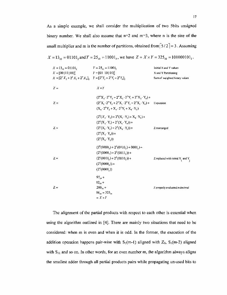
As a simple example, we shall consider the multiplication of two 5bits unsigned
binary number. We shall also assume that n=2 and m=3, where n is the size of the
small multiplier and m is the number of partitions, obtained fromp /2~| = 3. Assuming
Jf = 1310 =011012and7 = 25I0 = 110012, we have Z = XxY = 325l0 =1010001012.
Jf = 13,„=011012 7 = 2510 = 110012 Initial X and Y values
Z = [00|l l |01]2 Y = [01110101]* X and Y Partitioning
X = \2"X1 + 21X1+ 2°XI)]2 Y = [24 Y2 + 22Y, + 2°Y„]2 Sum of weighted binary values
Z = XxY
(24X2-24Y2 + 24X2-22Y,+24X2-Y0) +
Z= (22X,-24Y2 + 22X, •22Y, + 22X,-Y0)+ Expansion
(X0-24Y2 + X„-22Y, + X0-Y„)
(28(X2-Y2) + 24(X,-Y,) + X0.Y0) +
(26(X2-Y,) + 22(X, •¥„)) +
Z= (26(X,-Y2) + 22(X0-Y,))+ Zrearranged
(24(X2Y0)) +
(24(X„-Y2))
(28(00002) + 24(01102) + 00012) +
(26(00002) + 22(00112)) +
Z replaced with initial X. and Y. ' J
(26(00112) + 2:
(24(00002)) +
(24(00012))
97,„ +
12,o + 200,() +
16,o =325,,,
'(00102)) +
Z = 200,() + Z properly evaluated in decimal
6,0=32
= XxY
The alignment of the partial products with respect to each other is essential when
using the algorithm outlined in [4]. There are mainly two situations that need to be
considered: when m is even and when it is odd. In the former, the execution of the
addition operation happens pair-wise with Si(m-l) aligned with Zo, Si(m-2) aligned
with Sii and so on. In other words, for an even number m, the algorithm always aligns
the smallest adder through all partial products pairs while propagating un-used bits to

18
the result. In other words, the symmetry obtained through the second level operands is
used to efficiently perform the addition. The scheme presented in [4] reduces the
number of additions by half in each stage, given m is even.
On the other hand, when m is odd, the operands are no longer in pairs.
Consequently, the grouping operation which is used when m is even fails. To
compensate for that, the algorithm is modified and includes an extra level of addition.
Initially, Z0 is added to Si(m-l), skipping Sn and Si2 is added to Si(m-2). This is
iterated, with the summation of the second partial product postponed and performed at
the third level. Adding the first partial product to the last guarantees the use of the
smallest adder, similarly to having an even number of segments. In both cases, the
total number of addition levels required by the algorithm is L= |~log2 m +1].
Figure 3.6 shows the addition levels needed when the number of segments 'm' is
even and odd. The algorithm implements the adders in a binary tree format hence
reducing combinational delay. Since the adders are made out of logic cells, the largest
available in the design (SI 1) will constitute the critical path of the system in a
pipelined design. The critical delay obtained from adder SI 1 is represented by [16]:
' ADDER = '•OPCY "*" 'BYP ' V* "*" n \ m ~ *•)) + 'SUM
where IADDER is the total propagation time delay of the adder, topcy is the propagation
delay from the output of the function generator to the carry chain and tsuM is the
propagation delay from the carry chain onto the output.

NUMBER OF SEGMENTS 'm' IS EVEN 2™ LEVEL ADDITION 3RD LEVEL ADDITION R'» LEVEL ADDITIONtR-ILoG/nO+il)
<£- sfc-i
0- rC
i FINAL RESULT
COMBINATION OF PARTIAL PRODUCTS USING TWO OPERANDS ADDERS. REDUCING BY HALF THE NUMBER AT EVERY LEVEL
NUMBER OF SEGMENTS 'm' IS ODD 2™ LEVEL ADDITION 3™ LEVEL ADDITION R , a LEVEL ADDIT10N(R-|i.OG2(in)+51)
Sl(m-3)
Sl(m-2)
$-"
0
1
A -
S2(nv'2-1)
SRO
k M n-l) +
SI1
I FINAL RESULT
19
FIGURE 3.6 SEQUENCE OF ADDITION OPERATION FOR ALGORITHM [4] WHEN M IS EVEN
AND ODD
Even though the algorithm outlined in [4] tries to minimize adder lengths, it does
not control their implementation. More specifically, the methodology presented by
Shuli Gao et al. lacks implementation details at the architectural level. The authors
state that in their approach, adders at same level operate in parallel. Their algorithm
was demonstrated on the Spartan-3 FPGA which contains multiplier blocks only.
Also, for an m-segment multiplier, |~log2m + l] adder levels are needed to sum all
concatenated partial products generated by the small multipliers. The Spartan-3 FPGA
unfortunately does not include any high-speed adder block to perform the arithmetic
operation. This is one motivation around this thesis as it is believed that the use of
20
embedded high-speed adders will increase the performance of the system. The DSP48
block available in newer FPGA such as Virtex-4 provides this technological edge. The
algorithm outlined in this thesis also shows precisely how parallelism is achieved by
pipelining the system in a systematic way.
The performance of the method presented in [4] indicates better combinational
path delay and a smaller number of 4-input LUT used, compared to classical
implementations such as using the VHDL multiplication operator or the Xilinx
COREGenerator utility. The method in [4] relies heavily on parallelism and hence
implicitly makes use of a high number of registers. This amount relies on the size of
the input operand as well as the number of stages. For [4], this number is:
/=[log2m]
R = 2 2^(k-i-n)
i=\
where R=total register count, k=size of large multiplier, n=size of small multiplier,
m=number of segments. This number is non-negligible for large-input operands and
negatively affects the performance of the system by increasing the amount of
interconnects used in the FPGA while also raising power consumption.
Figure 3.7 shows that with smaller process technology such as 90nm (Virtex-4)
and 65nm (Virtex-5), interconnect delay contributes more to the overall system delay,
hence affecting overall system performance more than in past technologies[14].
Having a good placement of multiplier blocks together with pipeline registers will in
theory yield better overall performance compared to just algorithmic [4] and
architectural improvements.

21
Figure 3.7 Graph of gate and interconnect (wire) delay versus technology for Virtex
FPGA for a 16x2bit unsigned multiplier
3. 6 Summary of Multiplication Algorithms
This section introduced different long-integer unsigned multiplier architectures
that are suitable for FPGA implementation. These techniques use architecture-specific
enhancements that compensate for the main drawbacks of FPGA, which are limited
interconnect resources as well as large interconnect delay. In some cases, we even see
performance improvements when compared to other classic implementations such as
carry-look-ahead style multipliers, which when built using the constant-coefficient
method for example, will be much faster while requiring less space. Hence, knowing
the basic building blocks available in the FPGA will give a deep understanding and
the appropriate knowledge of how to fine-tune the device for an optimum operation.
The next section presents these features that are typical in modern FPGA which are
used extensively in arithmetic operations.

22
4 XILINX VIRTEX FAMILY FPGA
The Virtex FPGA family currently at its sixth generation evolved from the
XC4000E and XC5200 FPGA series. The first member of the family brought many
advanced features such as Delay-Locked Loops (DLL) and discrete RAM blocks
(BRAM). The internal wire bus was also re-designed to give a more accurate delay
model while providing shorter run time for the routing algorithm. Features like JTAG
programming and dedicated multiplication acceleration logic in the Configurable
Logic Block (CLB) [11] were also built in. Two generations later, the Virtex-2 series
were to incorporate discrete embedded multiplier blocks, which allowed faster DSP
operations such as digital filtering. Today, the newest Virtex-5 FPGA family is built
around third generation DSP blocks supported by fast routing busses and large amount
of embedded memory. The proposed set of algorithms uses DSP48 blocks released in
the Virtex-4 series, along with fast routing to improve on speed, area and power.
Modern FPGA chips consist of full-custom Intellectual Property (IP) blocks
surrounded by an array of logic elements interconnected by an intricate network of
busses. At the lowest level, the Logic Cell (LC) lays the foundation for digital
synthesis providing basic structures such as Look-up Tables (LUT), Flip-Flops (FF),
fast carry chains and multiplexers. Going up the hierarchy are pre-built high
performance IP blocks to execute DSP operations, discrete microprocessors for data
handling, high-speed interfacing and clock synthesis and re-conditioning. The
underlying interconnect also designed as a hierarchy, provides up to six different types

23
of routing. These are segmented and have switch boxes to control the flow of data
from one point to another.
FPGA are evolving every year as shown in Figure 4.1, with the newest Virtex-5
capable of 1,056 DSP48E slices along with 149,760 LUTs and FFs. The considerable
amount of DSP slices together with a high DSP-to-FF ratio (1:141) enables newer
algorithms to solve the problem of high speed long-word multiplication more
efficiently with the help of pipelining.
350
300
£ 250
| 200
£ 150 3
£ 100
50
Xilinx FPGA Trend
-Clock Frequency
- Density
VIRTEX-5 (6iuni) JfiKBIT EMBEDDED MEMORY 6-LUT LOGIC CELL PC] EXPRESS INTERFACE DSP4SE BLOCK.
VIRIEX-II(0.1!mui IBKBrT EMBEDDED MEMORY DICITALCLOCK MANAGER EMBEDDED MULTIPLIER DDR I/O
V1RTEX (0.2;ILHI) 4KBIT EMBEDDED MEMORY DIGITAL DELAY LOOP LMPRQVED ROUTING
VIRTEX-4 (90mn) EMBEDDED ETHERNET MAC DSP4S BLOCK ASMBL
VTRTEX-IIPROfO.IJimil POWER PC- EMBEDDED CPU ROCKET Gbpil'O TRIPLE DES SECURITY
250000
200000
5F
150000 o 'a o
100000 £
a a 50000
1990 1995 2000
Year
2005 V 0
2010
Figure 4.1 Trend for Xilinx FPGA during past 16 years
4.1 Logic Cells
The logic cell allows implementations of either combinational or sequential
circuits or a mixture of both. Combinational systems are implemented using 4-inputs
(up to 6 in Virtex-5) LUTs while state machines and registers are created out of built-
in Flip-Flops. The LUT element can also act as dynamic storage devices turning into
24
16bits shift registers. A group of logic cells sharing arithmetic resources is called a
slice. In a Virtex FPGA, logic cells within a slice have dedicated carry lines as well as
shared inputs. This enables the designer to implement arithmetic operations such as
addition and multiplication with small delay penalty while extending the size of the
operation. Also, slices are grouped into Configurable Logic Blocks (CLB) and share
routing structures.
The basic structure of the logic cell has evolved from a simple two-cell CLB to
four then eight cells. The progression among the Xilinx Virtex FPGA family is shown
in Figure 4.2, where differences between architectures are highlighted. In addition,
arithmetic capability is enhanced with the inclusion of XOR and AND gates for
arithmetic addition (Full-Adders based) and 1-bit multiplication respectively. Initially,
the XC4000E FPGA included a dedicated carry path that introduced little delay in
arithmetic operations. This has since then been added to all subsequent FPGA
families. Finally, the newest Virtex-5 FPGA provides faster overall arithmetic
operation since the carry path spans four logic cells compared to two in the previous
families. This reduces by half the amount of interconnect delay that would be present
should the operation be implemented in previous Virtex families.

25
CIN XC4000 CLB
1:2 SLICE TO LOGIC CELL RATIO 1:1 SLICE TO CLB RATIO 4 INPUT LUT FAST CARRY CHAIN CARRY CHAIN HEIGHT: 2 CELLS
Figure 4.2 Xilinx FPGA logic cell evolution during past 15 years
4. 2 Virtex Hardware Arithmetic
High performance arithmetic operation is achieved through different architectural
speed-up techniques built in the Virtex architecture. A logic cell contains extra 2-
inputs AND and XOR gates, which process incoming bits, for multiplication and
addition without committing an LUT [12]. This makes the design area efficient while
reducing the combinational delay. Since most hardware multiplication algorithms are
addition based, performance gain is further obtained when multiplication operations
use adder blocks. The knowledge of FPGA infrastructures also enables an efficient
implementation of arithmetic operations. For instance, addition operations are
accelerated through the use of high-speed carry chains [15] which span the vertical
1:2 SLICE TO LOGIC CELL RATIO 2:1 SLICE TO CLB RATIO 4 INPUT LUT FAST CARRY CHAIN ADDITIONAL XOR ADDITIONAL AND CARRY CHAIN HEIGHT: 2 CELLS
VIRTEX-2 CLB
1:2 SLICE TO LOGIC CELL RATIO 4:1 SLICE TO CLB RATIO 4 INPUT LUT FAST CARRY CHAIN ADDITIONAL XOR ADDITIONAL AND DYNAMIC SHIFT REGISTER (LUT) CARRY CHAIN HEIGHT: 2 CELLS
1:4 SLICE TO LOGIC CELL RATIO 2:1 SLICE TO CLB RATIO 6 INPUT LUT FAST CARRY CHAIN ADDITIONAL XOR ADDITIONAL AND DYNAMIC SHIFT REGISTER (LUT) CARRY CHAIN HEIGHT: 4 CELLS
FPGA LOGIC CELL EVOLUTION

26
height of the chip while proper placement of arithmetic cells decreases interconnect
delay if adjacent cells are packed together in a CLB. The proposed placement
algorithm combines layout information with the HDL code so that an optimum
placement is achieved within the CLB. The algorithm then places larger CLB based
blocks in an optimal arrangement so as to decrease interconnect delay.
Figure 4.3 gives the internal structure of a CLB built in the Virtex FPGA. It shows
how a single slice can implement a 3 x 1 bit multiplier using the adder cell (4-LUT,
XORCY, MUXCY) together with an extra AND gate (MULTAND). This can be
furthermore cascaded to extend the length of the multiplier. The critical path is along
the carry propagate chain and is obtained from:
*MULT_2N = hw "*" 'BXCY ' nVBYp) + VLO + *BXCY
where tMULT_2N is total propagation delay of the 2xN multiplier, tiLo is the propagation
delay of the 4-inputs look-up table (LUT), tBxcY is the propagation delay of output
BX of LUT onto the carry chain and IBYP is the propagation delay per carry-chain
multiplexer.
5x2BITS UNSIGNED MULTIPLIER
*>-r r-
SSoFK MULT AND
A , — r B, n
<R5joFh
A, B, A° B
4-LUT
)E>̂
INTERNAL VIEW OF SLICE FOR BITS A..A, AND A, INTERNAL VIEW OF LOOK-UP TABLE (LUT)
Figure 4.3 Hardware dedicated for arithmetic operations in Virtex FPGA

27
Conventional synthesis tool such as XST uses this technique to create adders and
eventually allows multipliers of arbitrary length to be created. This is a limitation
since higher performance can be achieved if the tool is aware of implementations
based on dedicated arithmetic blocks such as the DSP48.
4. 3 Xilinx DSP48 Arithmetic Block
The partition algorithm outlined in this thesis is based on the DSP48 block found
in the Virtex-4 FPGA. Also known as DSP48 tile, the block contains a multi
functional arithmetic unit capable of 18bits signed multiplication as well as three
operands 48bits sign-extended addition-subtraction-accumulator. The unit is
optimized for low power, high speed operation and offers pipelining at inputs,
intermediate levels and outputs. Internally, the DSP48 tile includes two slices each
with a set of multiplier and adder. The slice pair also shares internal connections
which are used when arithmetic operations exceeding the normal size of the slice are
implemented.
As shown in Figure 4.4, the internal structure of a DSP48 slice reveals that the
three operands 48bits adder can only add two operands if used with the multiplier
since the two partial products generated from the multiplier block are combined by the
adder. The proposed algorithm uses internal pipelining registers when required for the
highest performance.

28
DSP SLICE 1 PIPELINE REGISTER
*^3J> PIPELINE REGISTER
iOffi PIPELINE REGISTER
-*dl-b
E PIPELINE REGtSTER ^M>r 25X18 MULTIPLIER
C
PIPELINE REGISTER
^*n±feD ^r 4g. PCW
DSP SLICEO PIPELINE REGISTER '3
"-ffl PIPELINE REGISTER
PlPELlTiE REGISTER ^HW>n
rPffi 2?X18MULTIPLIER
PIPELINE REGISTER
a^rifeD ~^r
c
Figure 4.4 Internal view of Virtex-4 DSP48 tile (block) [17]
Figure 4.5 gives the internal view of a Xilinx Virtex-4 FPGA chip, as obtained
from FPGAEDITOR [30]. The height of a DSP48 tile is equivalent to that of four
CLBs [34], or eight slices. Since one tile consists of two DSP48-slices, we can
calculate the height of a single DSP48 slice to be that of 4 logic-slices, with a width of
1 logic-slice. This is clearly indicated in Figure 4.5.
Figure 4.5 DSP48 slice to CLB area ratio, as shown in Xilinx FPGAEDITOR [35]

29
The internal operation of the DSP48 tile is fully programmable with the help of
OPMODE and CARRY bits. The OPMODE defines how inputs X, Y and Z are used.
X and Y each has two bits dedicated to their internal configuration and can be
programmed in six different modes. The output from the X multiplexer can be zeroed,
coming from the first partial-product multiplier, coming from port P or be
concatenated with B. Similarly, the Y multiplexer allows only three valid
combinations; zeroed, propagating the second partial-product or outputting port C.
The OPMODE also controls the Z multiplexer and has 3bits reserved for it. Out of
eight possibilities, only six are used with the actual combination shown in Table 4.1.
TABLE 4.1 VALID OPMODE FOR DSP48 BLOCK, WITH RESPECT TO Z MULTIPLEXER [18]
OPMODE PROGRAMMING BITS
Z
000
001
010
011
100
101
110
111
Y
XX
XX
XX
XX
XX
XX
XX
XX
X
XX
XX
XX
XX
XX
XX
XX
XX
Z MULTIPLEXER OUPUT DRIVING
ADDER/SUBTRACTOR
ZERO (DEFAULT)
PCIN
P
C
ILLEGAL SELECTION
PCIN SHIFT
P SHIFT
ILLEGAL SELECTION
Table 4.2 gives the configuration bits of the second and third operand multiplexes
driving the adder (MUX X, MUX Y). In order to program the DSP block to
perform/ = P±(AxB + ClN), the following bits would be needed in the OPMODE
register: 0100101.

30
TABLE I. TABLE 4.2 VALID OPMODE FOR DSP48 BLOCK, WITH RESPECT TO X AND Y MULTIPLEXER [19]
OPMODE BITS
Z
XXX
XXX
XXX
XXX
XXX
XXX
XXX
XXX
Y
XX
01
XX
XX
00
01
10
11
X
00
01
10
11
XX
01
XX
XX
Z MULTIPLEXER OUPUT DRIVING
ADDER/SUBTRACTOR
ZERO (DEFAULT)
MULTIPLIER OUTPUT (PARTIAL PRODUCT 1)
P
A CONCATENATE B
ZERO (DEFAULT)
MULTIPLIER OUTPUT (PARTIAL PRODUCT 2)
ILLEGAL SELECTION
C
Finally, Table 4.3 shows configuration bits for the CARRYINSEL register which
controls how the carry input is connected to the adder. Furthermore, the mode of
operation for the carry input is dependent on the value entered in the OPMODE
register.
TABLE 4.3 CARRYINSEL CONTROL BITS WITH CORRESPONDING OPMODE OPERATION [20]
CARRYINSEL [1:0]
00
01
01
10
11
10
11
OPMODE
XXXXXXX
Z MUX OUTPUT = P OR SHIFT (P)
Z MUX OUTPUT = PCIN OR SHIFT(PCIN)
X AND Y MUX OUTPUT = MULTIPLIER PARTIAL
PRODUCTS
X AND Y MUX OUTPUT = MULTIPLIER PARTIAL
PRODUCTS
X MUX OUTPUT = A:B
X MUX OUTPUT = A:B
CARRY SOURCE
CARRYIN
~P[47]
~PCIN[47]
A[17] XNOR B[17]
A[17] XNOR B[17]
~A[17]
~A[17]
COMMENTS
GENERAL FABRIC CARRY SOURCE (REGISTERED OR NOT)
ROUNDING P OR SHIFT(P)
ROUNDING CASCADED PCIN OR SHIFT(PCIN) FROM ADJACENT
SLICE
ROUNDING MULTIPLIER (MREG PIPELINE REGISTER DISABLED)
ROUNDING MULTIPLIER (MREG PIPELINE REGISTER ENABLED)
ROUNDING A:B (NOT PIPELINED)
ROUNDING A:B (PIPELINED)

4.4 Interconnect
31
The present work describes a placement algorithm which requires a clear
understanding of the wire infrastructure available in the Virtex FPGA. The
interconnect network can be seen as a hierarchy of wire connecting CLBs, DSP48s,
clock generators, Input/Output ports and so on together.
Hierarchy of interconnect [13]:
(a) Local Routing (High speed)
1. 1 Connection between LUTs, Flip-Flops and General Routing Matrix
(GRM) switch box.
1. 2 Internal CLB feedback routes connecting output to LUT input with
minimum delay.
1. 3 Direct path between horizontal adjacent CLBs (Virtex).
1. 4 Direct path between adjacent CLBs in sixteen directions (Virtex-II and
above) [21].
(b) General Purpose Routing (Low-medium speed)
1. 5 Routing between GRM switch boxes.
1. 6 Single-length lines connecting adjacent GRMs in four directions.
1. 7 Buffered Hex lines connecting GRM to other GRMs placed six blocks
further in each of the four directions.
1. 8 Buffered Longlines bidirectional wires that span the full length of the
FPGA chip either horizontally or vertically.
(c) Global Routing (Low skew)

32
1. 9 Primary global routing includes high-fanout signal lines such as clock
networks and are designed to have minimal skew.
1. 10 Secondary global routing is mainly secondary clock routing consisting
of backbones lines distributed across the top and bottom portion of the
FPGA. They connect to Longlines interconnect,
(d) Dedicated Routing (High speed)
1.11 Constrained interconnect for the arithmetic carry chain.
1.12 Horizontal routing for three-state busses.
1.13 Dedicated SOP chain for each slice row [21].
1.14 Shift-chain routing, one per CLB [21].
The proposed placement algorithm relies on adjacently placed CLBs to minimize
interconnect delay and consequently falls into the Local Routing class. Moreover,
Dedicated Routing is implicitly used by the carry chain infrastructure in the
realization of adders and DSP48 blocks. Figure 4.6 shows fives types of routing
technologies found in the Virtex-2 FPGA. Since the Virtex-4 is based on the same
routing infrastructure, a placement algorithm that first uses local, then direct, double,
hex and finally long lines will reduce overall interconnect delay and hence improve on
timing performance.
Figure 4.6 Different interconnect classes found in the Virtex family of FPGA [21].

4. 5 Congestion
33
Congestion is a concentration measure of active interconnects in part of the
routing resource. It negatively affects performance since a congested region is very
unlikely to allow free routing of wires or would provide so with heavy delay penalty.
Congestion also decreases area utilization because CLB is eventually used in the most
congested regions as passthrough logic, logic that acts as simple wires to add extra
routing resources. This quick-fix increases the interconnect delay significantly and
should be used as a last resort.
Anticipating congestion and increasing the region allocated to routing resources
minimize most of the effect. The placement algorithm uses congestion as an objective
function, where a slack region between CLBs is added if congestion is high. The
placement algorithm models congestion using graph theory with congestion defined as
the number of vertices sourced or sank at a node per unit area.
4.6 Summary of Techniques
This chapter presented the Virtex FPGA family at the low level, giving
information about logic cell, arithmetic implementation techniques, the DSP48 block,
the routing infrastructure and finally congestion. The focus of this thesis is to present
an algorithm that will increase performance of long-integer multiplication operations.
Using DSP48 blocks provide the user with processing elements that have the lowest
delay, power and area. On the other hand, care should be taken in order not to increase

34
interconnect delay which would negate the use of DSP48 blocks. Hence, knowledge
of the routing hierarchy as well as an understanding of congestion is essential.

35
5 PARTITION ALGORITHM FOR VIRTEX-4 FPGA
The algorithm for partitioning unsigned multiplication operations is originally
proposed by Shuli-Gao et al [4] and solves the problem using small but high-
performing DSP blocks abundantly found in modern FPGAs. The algorithm is generic
in nature and hence does not specify with what technology the actual addition and
multiplication operations are implemented. The algorithm is also modified depending
on whether m is even or odd, m being [£/«], k being the size of the large multiplier
input operand and n being the size of the small multiplier input operand. In case of m
being odd, an extra adder level is needed. Finally, the generated multiplier relies on
pipelining to reduce combinational delay as the circuit is in the form of an array
multiplier, similar to the Carry Save Array multiplier. The algorithm can be expressed
as:
Z = X.Y = Yj2{ki)Xi^2(k%m =
i=o ;=o y=o
where Z is the output of the large integer multiplier, k is size of the operand at the
large multiplier input and n is size of the small multiplier.
Our proposed algorithm adapts [4] to use the more efficient DSP48 block
available in Virtex-4 FPGAs. This gives better overall performance since DSP48 is
superior to the multiplier circuits available in the Spartan-3 FPGA. The physical
location of hardware blocks is also crucial in order to get an optimal result. Using
DSP48 allows the software mapper to lock blocks in reserved vertical regions which

36
minimizes the amount of interconnect. Since the partition algorithm does not include
locality information, a second algorithm is described in this thesis that adds placement
information. This reduces interconnect delay caused by pipelining structures used by
the partition algorithm as well as in groups participating in the critical path.
5.1 Details of Operation
From the original algorithm, dataflow can be separated into different operation
levels. This is also true in the proposed partition algorithm and initially, the
multiplication of all sub-words of length m, m being the length of our DSP48 block
operand, into their respective squares, Zo, is summed to the product of Xj with Yj+i
and Xj+i with Yj, where Q<i < N, N=number or levels of multiplication, Xj and Yj
are sub-words from the long-integer numbers, into the partial word, Zi. At the third
level, Zi is added with Xj*Yj+2 and Xi+2*Yi where 0<z<JV-l . Additions at each
stage is repeated in the same way until only a single addition/multiplication level is
left which happens at i=0. This generates the middle range values for the
multiplication. At each level, an extra adder is required to sum the carry bit of the
current level with the most significant bit of the previous partial product.
Since DSP48 multipliers operate with signed 18bits values, our implementation
can only use the lower 17bits with the sign (most significant) bit connected to logic
'0'. This results in the length of the input operand 'm' being equal to 17. The
proposed algorithm performs all the required steps for partitioning long integer
numbers including the creation of interconnects between DSP48 blocks and inclusion
of intermediate pipeline registers.

37
The multiplier as well as adder blocks can be reorganized as shown in Figure 5.1.
There is also a noticeable change in the proposed architecture, which removes the
necessity of having to deal with odd and even number of segments (m). This is
required because the original architecture does not allow for a direct combination of
adders and multipliers blocks into a unified module.
Figure 5.1 Technology mapping of [4] into proposed architecture for a 68bits
unsigned multiplier
As presented in this algorithm, the innovative aspect is the mergence of the
addition block together with the multiplication block into a single entity: the
Arithmetic Cell A (ACA). This is very different from the architecture proposed in [4],
where no implementation details are given. A single DSP48 tile can therefore be
38
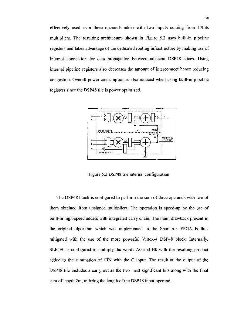
effectively used as a three operands adder with two inputs coming from 17bits
multipliers. The resulting architecture shown in Figure 5.2 uses built-in pipeline
registers and takes advantage of the dedicated routing infrastructure by making use of
internal connection for data propagation between adjacent DSP48 slices. Using
internal pipeline registers also decreases the amount of interconnect hence reducing
congestion. Overall power consumption is also reduced when using built-in pipeline
registers since the DSP48 tile is power optimized.
KE>Og±)0 :DSP48SLICE1
iS-
PCIN:
KH^ ;DSP48SLICE0
i INTERNAL I ROUTING
Figure 5.2 DSP48 tile internal configuration
The DSP48 block is configured to perform the sum of three operands with two of
them obtained from unsigned multipliers. The operation is speed-up by the use of
built-in high-speed adders with integrated carry chain. The main drawback present in
the original algorithm which was implemented in the Spartan-3 FPGA is thus
mitigated with the use of the more powerful Virtex-4 DSP48 block. Internally,
SLICEO is configured to multiply the words AO and BO with the resulting product
added to the summation of CIN with the C input. The result at the output of the
DSP48 tile includes a carry out as the two most significant bits along with the final
sum of length 2m, m being the length of the DSP48 input operand.

39
The functionality of the DSP48 block is programmed at compilation time with
attributes for the operation mode and carry type written as attributes in the hardware
descriptive language source. Table 5.1 gives binary values for the OPMODE as well
as that of the CARRY register. Once set, they will control how the internal datapath of
the DSP48 is setup and also, which registers are enabled.
TABLE 5.1 OPMODE/CARRY CONFIGURATION BITS FOR SLICEO AND SLICEI
SLICE CONFIGURATION
SLICEO SLICEI
CONFIGURATION BITS OPMODE
6 0 0
5 1 0
4 1 1
3
0 0
2 1 1
1
0 0
0 1 1
CARRY 1
0 0
0
0 0
5. 2 Arithmetic Ceil A Block
The proposed algorithm defines two types of arithmetic cells which are based on
the Virtex-4 DSP48 block. Arithmetic Cell A (ACA) (Figure 5.3) encapsulates the
operation:
P = (4,-50) + (4-51) + C Eq. 1
The total latency is equal to that of SLICEO combined with SLICEI and results in
4 registers. The external registers on AO, BO, C, Al, Bl inputs are needed in order to
synchronize the arrival of data at the DSP48 tile, with respect to their internal latency.
Furthermore, registers REGc and REGp are optional. REGp is needed when ACA is
used internally and not in the last column while REGc is required at the second level
only. The proposed algorithm generates the correct ACA block with the use of Eo
(Enable of REGc) and Ei (Enable of REGp). REGP is also of constant depth (4
registers) which equals to the latency of one DSP48 tile. The input of REGp is taken

40
from the most significant 17bits of output P and ranges from bit Pn to bit P33. The
output of REGp is then reconnected to signal P, hence delaying only the upper part of
P when needed. If REGp is disabled, then the output of the DSP48 tile bypasses REGp
and connects directly to the product P. COUT represents carry-out bits and connects
the two most significant bits of P to adjacent ACA and ACB blocks. CIN is the carry
input of ACA and is internally pipelined by the DSP48 slice.
AO . : ,
BO . : ,
' .
c . •• ,
3 4 •
Al , : , 17 ;
17 ;
73
n
73
CD
"73 m 0
rv -73 1II
n 73 111
0 Lc
• •••
• ••*
REG REG
• ••*
• •••
• •••
tency D.
m §11
73 111
n 73 111 n
4t La
REG REG
73
O
REG REG
tency
t
?t
?t
2t
O N -
\
{*> s
REG 1
REC,. IMPLEMENTED WHEN
RECC_EN='r ELSE BYPASS
REG,, IMPLEMENTED WHEN
REGP_EN=l ELSE BYPASS
\
®-s
REG |
DSP48 SlICEO;
>+Vn ^
r
REG
t A
L 1
£>
REG
t j
DSP48 SLICE!;
M 4t
\ \
Figure 5.3 Internal view of Arithmetic Cell A block
5. 3 Arithmetic Cell B Block and Cascade Register
The Arithmetic Cell B (ACB) (Figure 5.4) performs the operation R = X + Y(Eq.
2). Input X is unregistered and connects directly to the first operand of the adder
block. Input Y conversely has registers m-bits wide and of depth Do which connects to
the second operand of the adder. The result R at the output can also be registered with
a depth of Dj. A single DSP48 slice is sufficient to perform the addition operation

41
together with some pipelining (4 registers). Alternatively, the adder can be constructed
using logic cells.
ARITHMETIC CELL 8
Figure 5.4 Internal view of Arithmetic Cell B block
The proposed partitioning algorithm finally makes use of a third type of block, the
Cascade Register (CR) (Figure 5.5). It consists of a series of cascaded registers of
fixed width (m) and of variable depth D2.
Do=D.=D,=0 ^ BYPASS REGISTER CASCADE REGISTER
Figure 5.5 Internal view of Cascade Register block
5. 4 Partition Algorithm Description
When run at a high level, the time complexity of the algorithm is in 0(N2) while
requiring constant amount of space, hence in 0(1) space-wise. Initial parameters are
needed for the input length of operands (n) and the size of the small multiplier (m).
The algorithm is described in pseudo code format in the Algorithm la listing. First,
the number of levels (N) is calculated in line 1. Then, input segments of length m are
squared together to produce Zo (lines 2 to 4). This is accomplished by using N
42
unsigned multipliers created from DSP48 tiles, where N=number of levels, resulting
in an aggregated 2mN partial product word, where m is the small multiplier operand
size, representing the square of the input values grouped with length 2m.
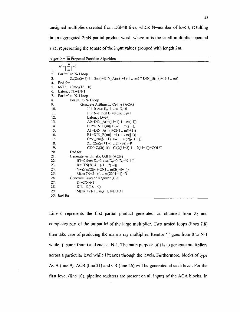
Algorithm la Proposed Partition Algorithm
2. For i=0toN-l loop 3. Z0(2m(i+1)-1 .. 2mi)=DIN_A(m(i+l)-l .. mi) * DIN_B(m(i+l)-l .. mi) 4. End for 5. M(16..0)=Zo(16..0) 6. Latency D2=2N-1 7. For i=0 toN-1 loop 8. For j=i toN-1 loop 9. Generate Arithmetic Cell A (ACA) 10. If i=0 then E0=l else E0=0 11. If i=N-l then E,=0 else E,=l 12. Latency D=i+j 13. A0=DIN_A(m(j-i+l)-l .. m(j-i)) 14. B0=DIN_B(m(j+2)-l .. m(j+l)) 15. Al=DIN_A(m(j+2)-l .. mQ+1)) 16. Bl=DIN_B(m(j-i+l)-l .. m(j-0) 17. C=Zi(2mG-i+l)+m-l .. m(2G-i)+l)) 18. Zi+1(2mG-i+l)-l .. 2mG-i))=P 19. CIN=C,(2G-i)); Q(2G-i+2)-l .. 2G-i+l))=COUT 20. End for 21. Generate Arithmetic Cell B (ACB) 22. If i=0 then D0=3 else Do=0; D,=N-i-l 23. X=CIN(2G-i+l)-l .. 2(j-i)) 24. Y=Zi(m(2G-i)+2)-1 .. m(2G-i)+l)) 25. M(m(2N+2-i)-l..m(2N-i+l))=R 26. Generate Cascade Register (CR) 27. D2=2(N-i-l) 28. DIN=Zi(16..0) 29. M(m(i+2)-l .. m(i+l))=DOUT 30. End for
Line 6 represents the first partial product generated, as obtained from Z0 and
completes part of the output M of the large multiplier. Two nested loops (lines 7,8)
then take care of producing the main array multiplier. Iterator T goes from 0 to N-l
while ' j ' starts from i and ends at N-l. The main purpose of j is to generate multipliers
across a particular level while i iterates through the levels. Furthermore, blocks of type
ACA (line 9), ACB (line 21) and CR (line 26) will be generated at each level. For the
first level (line 10), pipeline registers are present on all inputs of the ACA blocks. In

43
every step, the latency D of the block is calculated with the formula D = i + j , while
inputs to the ACA block are taken either from the large input word (m) or from the
result obtained at the previous level (line 13 through 17). The output at each ACA
block from one level consists of Z\+\ and carry-lines, which are propagated through
adjacent ACA blocks. At each level, an ACB-CR block pair is required to sum the
current carry information with the previous data obtained and to delay the resulting
data respectively (line 21 to 28). ACB blocks are positioned at the end of the column
while CR blocks are placed at the beginning. Finally, the output from both CR and
ACB blocks drives the final output of the large multiplier (M).
Figure 5.6 shows a long-integer multiplier of size 68bits generated using the
proposed algorithm. The structure consists of 4 levels, including the squarers at the
input, and intermediate levels consisting of ACA, ACB and CR blocks. The output is
obtained at M after 5 latency cycles.
E.- ' E."1
E„- l E,-l D=l
Y<1
E,-l E,-l
DIN.A: XJX,X1X0 DIN_B Y Y.Y,Y DOUT M: M,M,M,M,M.r
-\m E,=REGC ENABLE E.-RECP ENABLE ACA - ARITHMETIC CELL A ACB = ARITHMETIC CELL B CR = CASCADE REGISTER
v XOTAO a— so
j - c ACA P
E.-0 E,=l 0=2
E,-0 E,-l
D.-0, D,- l
"04 A *
J D»4 E.-0 E,-0
Do-0, 0,-0
Figure 5.6 Long-integer 68x68bits multiplier generated by proposed algorithm

5. 5 Resources Utilization
44
The amount of FPGA resources needed for a multiplier generated by the algorithm
can be derived in terms of the input word length n, the DSP48 operand size m and the
number of levels N.
Number of levels (N) = n
m - 1
Number of input multipliers = N+l
N(N +1) Number of Arithmetic Cell A blocks = — -
2 Number of Arithmetic Cell B blocks = N
Number of DSP48 slices used (ACB implemented with logic cells) =
For a pipelined design, the algorithm further defines the
DSP48 block latency (L) = 4
Number of Cascade Register blocks = N
Total pipeline latency = 4(2N-l)
Eq. 3
Eq. 4
Eq. 5
Eq. 6
= (N +1)2 Eq. 7
following terms:
Eq. 8
Eq. 9
Eq. 10
5. 6 Performance Equations
The following equations describe the performance of the proposed partition
algorithm when the width V is changed, while m, the size of the DSP48 input is kept
constant. In the equations, L=4 and represents the latency of a DSP48 block.

45
Number of levels (N) = r- - l
n m
-1 Eq. 11
N2
Number of multiplier blocks = \-3N + \ Eq.
N-lN-\
Number of registers for pipeline design= mL((^ ^ 4(/' + j) + 1) + N2 - N -I) Eq. y=0 i=j
Worst case combinational delay TP=TDSPD0 BPL ns Eq.
Maximum frequency of operation FM^T= MHz Eq. T +T +T 1DSPCKO _ PCOUTP ^ 1 DSPDO _BPL^ 1DS
12
13
14
15
, w h e r e TDSPD0 BPL,TDSPCK0 PC0UTP and TDS are defined in [33].
5. 7 Non-Pipeline Design
From Eq. 13, a generated design has an area that exhibits a quadratic behaviour in
N. Instead, the design can also be used with less pipelining stages. This is a trade-off
of area against speed of operation. As such, the proposed partition algorithm is
modified for a non-pipelined design, with the configuration of the DSP48 blocks also
changing in order to reflect this, as shown in Algorithm lb.

46
Algorithm lb Proposed Partition Algorithm (Non-Pipelined)
1.
_- -, N = n
m - 1
2. For i=0toN-l loop 3. Z0(2m(i+1)-1 .. 2mi)=DIN_A(m(i+l)-l .. mi) * DIN_B(m(i+l)-l .. mi) 4. End for 5. M(16.. 0)=Zo(16..0) 6. For i=0toN-l loop 7. Forj=i toN-1 loop 8. Generate Arithmetic Cell A (ACA) 9. AO=DIN_A(m(j-i+l)-l .. m(j-i)) 10. B0=DIN_B(m(j+2)-l .. m(j+l)) 11. Al=DIN_A(m(j+2)-l .. m(j+l)) 12. Bl=DIN_B(m(j-i+l)-l ..m(j-i)) 13. C=Zi(2mG-i+l)+m-l .. m(2(j-i)+l)) 14. Zi+i(2m0-i+l)-l •• 2m(j-i))=P 15. CIN=Ci(2G-i)); Cj(20-i+2)-l .. 2(j-i+l))=COUT 16. End for 17. Generate Arithmetic Cell B (ACB) 18. X=CIN(2(j-i+l)-l .. 2(j-i)) 19. Y=Z,(m(2(j-i)+2)-l .. m(2(j-i)+l)) 20. M(m(2N+2-i)-l .. m(2N-i+l))=R 21. Generate Cascade Register (CR) 22. M(m(i+2)-l .. m(i+l))= Z,(16 .. 0) 23. End for
Synthesis results as obtained from the Xilinx ISE tool [30] show that timing
performance for the proposed algorithm decreases when compared to an
implementation such as using the multiplication operator as obtained from the HDL
library. The timing result of our proposed implementation is still better than solutions
obtained from COREGenerator.
TABLE 5.2 PERFORMANCE RESULTS FOR COMBINATIONAL DELAY, NON-PIPELINED DESIGNS
Multiplier Width Proposed Algorithm
Implementation using VHDL multiplication operator
COREGenerator
34bits 10.195ns
9.514ns
10.596ns
64bits 22.948ns
15.190ns
40.742ns
136bits 73.069ns
21.925ns
N/A
221bits 111.428ns
28.485ns
N/A

47
TABLE 5.3 PERFORMANCE RESULTS FOR AREA UTILIZATION, NON-PIPELINED DESIGNS
Multiplier Width Proposed Algorithm
Implementation using VHDL multiplication operator
COREGenerator
34bits 16 Slices
16 Slices
16 Slices
64bits 64 Slices
143 Slices
64 Slices
136bits 256 Slices
800 Slices
N/A
221bits 676 Slices
2288 Slices
N/A
As shown in Table 5.3, a design generated by our algorithm (non-pipelined) does
not consume any logic cell with all arithmetic operations taking place in DSP48
blocks. The table uses the logic slice to DSP48 slice ratio of 4:1, as introduced in
Chapter 4.3.
The delay product (AT2) is given in Figure5.7 and shows the performance of three
non-pipeline implementation methods. When measured in AT2, the proposed
algorithm for non-pipelined designs is actually worse than HDL and Coregen
implementations. This is so since the DSP48 block is highly optimized for pipelining
operations, which is not the case here.
10000000
1000000 -
= 100000 -•D o
1 10000 -n 3
% 1000 -J2 o a 2 100-
10 -
1 -
0 50 100 150 200 250
Size of Operands (bits)
Figure 5.7 Area-Delay product for non-pipeline multipliers
- coregen
- proposed algorithm
• hdl implementation

5. 8 Results
48
The partition algorithm presented was originally designed to use a pipelined
architecture. This was decided since the building block itself, the DSP48, is optimized
for pipelining under which it will operate at a theoretical 500MHz. With the following
figures, the reader will get an idea of how well multipliers generated by the algorithm
perform against classical implementations which are readily available to the designer.
For comparison, designs with input width of 34bits, 68bits, 136bits and 221 bits were
chosen because they are very close to practical multiplier lengths while at the same
time, are multiplies of the DSP48 block input size. Classical implementations were
obtained from two sources:
(a) Components generated from the COREGenerator utility [30].
(b) VHDL synthesis of the multiplication operator, as provided by the
language's arithmetic library.
Also, for comparison, results from the original partition algorithm are included to get
an idea of the improvement that the proposed algorithm brings to the end user. Graphs
for combinational path delay, amount of logic slices, DSP48 slices and power
dissipation against changing input sizes are given. Area-Delay product (AT2) is given
to understand where the proposed partition algorithm is best at, either in terms of
delay or area. The graph of interconnect and gate delay is given which shows where
improvements exist.
Data for the given graphs were obtained from report files generated by the
Mapping and Place-and-route tools and included area and delay respectively.

5.8.1 Combinational path delay
49
Combinational delay of the critical path in the multiplier is given for changing
input sizes. The critical path includes gate as well as interconnect delay. Figure 5.9
shows that multipliers generated using our algorithm outperform other methods
available. Data for "Coregen" and "Original algorithm" were either unrealizable or
not available for input sizes above 64bits.
100
a
t 10 n c o
.Q E o u
- Proposed multiplier
Coregen multiplier
• HDL multiplier
Original algorithm
16 32 64 128
Size of Operands (bits)
221
Figure 5.8 Combinational path delay for different sized inputs

50
5.8.2 Virtex-4 logic slice utilization
The amount of resources in terms of slices used is presented in Figure 5.9. The
number of DSP48 used is also factored in with an equivalent number of four slices per
DSP48 block used. The proposed algorithm uses a large number of logic slices to
implement pipeline datapaths, which is revealed in the graph.
100000
10000
t x a
5
!
1000
100
10
- Proposed multiplier
Coregen multiplier
• HDL multiplier
Original agorithm
. » > '
16 32 64 128
Size of Operands (bits)
221
Figure 5.9 Amount of Virtex-4 slices used against different sized inputs
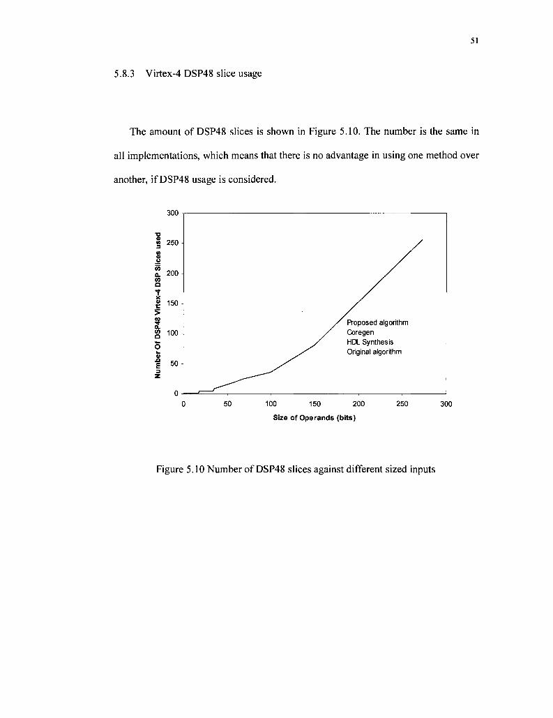
51
5.8.3 Virtex-4 DSP48 slice usage
The amount of DSP48 slices is shown in Figure 5.10. The number is the same in
all implementations, which means that there is no advantage in using one method over
another, if DSP48 usage is considered.
300
•D
» 250 </> 0 o 55 o. 200 if) a
| 150 !> 00
2 g 100
f 50
Proposed algorithm Coregen HDL Synthesis Original algorithm
100 150 200
Size of Operands (bits)
250 300
Figure 5.10 Number of DSP48 slices against different sized inputs

52
5.8.4 Area delay (AT ) product
The area delay-squared product is a performance measure used to benchmark
designs. Multipliers of various sizes generated by the proposed algorithm are hence
evaluated using this method and compared with more commonly used HDL and
Coregen implementations (Figure 5.11). Also, results obtained from the original
algorithm [4] are included.
10000000
1000000
T> 3 •D O Q.
ared
3 a-(/> >. n a a a
Are
100000
10000
1000
100
10
- Froposed multiplier 1
Coregen multiplier 3
• HDL multiplier 2
Original agorithm
16 32 64 128
Size of Operands (bits)
221
Figure 5.11 Area Delay product (AT2) performance measure

53
5.8.5 Power dissipation
Power dissipation is obtained from the Xilinx Xpower [36] software. The utility
takes into account static as well as dynamic power dissipation. Results were obtained
for HDL, Coregen and the multipliers generated by the proposed algorithm (Figure
5.12). The frequency of operation was fixed at 50MHz while the activity rate was set
at 50%.
12
10
5. 8
S 4 o
Q.
FVoposed multiplier 1
Coregen multiplier 3
HDL multiplier 2
20 40 60 80 100
Size of Operands (bits)
120 140
Figure 5.12 Power dissipation for different sized inputs
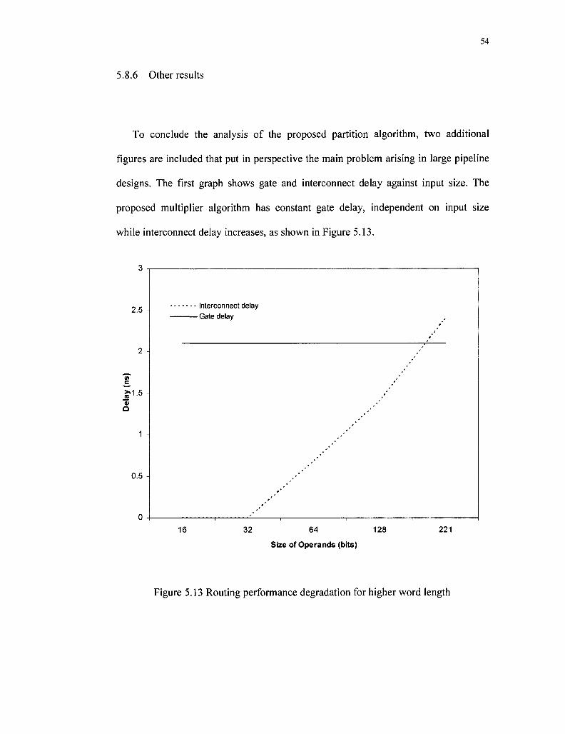
54
5.8.6 Other results
To conclude the analysis of the proposed partition algorithm, two additional
figures are included that put in perspective the main problem arising in large pipeline
designs. The first graph shows gate and interconnect delay against input size. The
proposed multiplier algorithm has constant gate delay, independent on input size
while interconnect delay increases, as shown in Figure 5.13.
2.5 -
2 -
in
c
0) Q
0.5
Interconnect delay - Gate delay
16 32 64 128
Size of Operands (bits)
221
Figure 5.13 Routing performance degradation for higher word length

55
Figure 5.14 shows the final placement of logic blocks along with DSP48 slices as
produced by the Xilinx place-and-route tool [30]. It shows the drawback associated
with the automated placement tool used, where logic placement is not relatively
placed with respect to DSP48 blocks.
Figure 5.14 Layout of placed 136xl36bits multiplier circuit inside a Virtex-4 FX140
FPGA

56
5. 9 Summary
The partition algorithm presented in this thesis uses DSP48 blocks efficiently to
create large-input unsigned multipliers. Figure 5.8 shows that the proposed solution
outperforms other methods if compared using critical path delay. Since the design is
heavily pipelined, improved delay performance comes at a price of higher logic-cell
consumption. Another performance measure (AT2) has been presented (Figure 5.11),
where it is shown that for input sizes of less than 64bits, the COREGeneator
implementation method was marginally better, while the proposed partition algorithm
has a much lower value for AT2 across all input sizes when compared to HDL
implementation using the multiplication operator. To conclude, problems arising when
doing pipeline designs are outlined and possible solutions to the placement problem
are further discussed in Chapter 6.

57
6 PLACEMENT ALGORITHM FOR LARGE-UNSIGNED MULTIPLIERS
Chapter 5 outlined a partition algorithm that can be used to develop arbitrary sized
multipliers based on small but efficient DSP48 arithmetic blocks available in the
Xilinx Virtex-4 FPGA. The improvement achieved is mainly dependant on the ability
to fit the algorithm presented in [4] into the architecture using both multiplier and
adder elements of the DSP48 slice. Even though the main cause of delay reduction is
the use of high-performance DSP blocks, delay is also minimized with the use of local
wire interconnect since a DSP48 block packs together a source (multiplier) along with
its sink (adder) in the same physical component and thus avoids using the FPGA
routing channels. The consequence of this improvement is also an increase in the
amount of wire in the multiplier design to connect ACA, ACB and CR blocks
together. This is shown at the end of Chapter 5 (Figure 5.13), where gate delay is
constant while overall interconnect delay actually increases almost linearly.
6.1 Introduction
The proposed partition algorithm needs only a timing constraint on the clock input
to generate a solution. The software auto-placer then decides where DSP blocks and
pipeline registers should be located. The running time to get a solution is generally
long because finding a possible placement is considered an NP-complete problem
[22]. The placement tool uses an algorithm which can be manually adjusted to find a
58
reasonable answer according to rules supplied by the designer such as high speed or
low power.
A long-integer multiplier generated by the proposed partition algorithm consists
mainly of DSP blocks connected to pipelining registers without any control logic. The
next improvement will be to place the various hardware blocks in an optimum
arrangement so that area, delay and power are minimized. A logical placement of
critical blocks will also reduce the set of solution which can be obtained, decreasing as
a result the running time of the Place-And-Route (PAR) algorithm used by the
implementation CAD tool and giving consistent timing results between PAR
iterations. A new placement algorithm is hence proposed which is partly based on the
greedy algorithm concept and uses property of the heterogeneous placement algorithm
proposed by Love Singhal et al. [23].
Figure 6.1 shows the required steps in order to partition and place an arbitrary
length multiplier with the proposed set of algorithms. The resulting design can either
be used as a single unit residing on the FPGA, as in the case of an arithmetic
accelerator, or alongside other systems, similar to a System-On-Chip (SOC)
methodology. In the case of a SOC design, the partitioning and placement algorithm
has to be executed first before any other placement in order to guarantee the highest
performance. The placement algorithm is also generic and can be ported across other
FPGA families (Virtex-2 and upwards).

59
DESIGN IMPROVEMENT WITH PROPOSED ALGORITHMS
PARTITION ALGORITHM
PLACEMENT ALGORITHM
NORMAL DESIGN FLOW
1 INITIAL MULTIPLIER SPECIFICATIONS: OPERAND SIZE
Figure 6.1 Typical design flow using proposed set of algorithm
6. 2 Placement Problem Formulation
A circuit generated by the placement algorithm consists primarily of nets and
modules. Modules can be either of type ACA, ACB or CR. ACA and ACB have
further restrictions to their physical location on the FPGA, DSP blocks being located
in dedicated DSP columns spanning the vertical height of the chip and have
input/output ports located to one side of the column. The placement problem is in
finding suitable locations for elements of the circuit that will either minimize or
maximize objective functions supplied by the designer, which are usually minimum
delay, minimum power and minimum area. The solution hence improves on the

60
original design according to the objective functions. Optimum placement can also be
seen as a search problem where a solution that satisfies all objective functions is
enough. The search space is very large in modern FPGA hence the reason why the
complexity is NP-complete.
Formally, the general placement problem can be written as follows. A circuit W is
a set containing nets and basic elements, the set of nets being./V = {./V1,./V2,...,./V,}
while the set of elements is2? = {E],E2,...,EJ}. Furthermore, a group of elements and
nets is called a module and the set of modules M = {MvM2,...,Mk}. We associate
with each module in M a subset of N and a subset of E which correspond to nets and
elements present in a particular module. Therefore, M, e M,NM c N where M,is a
module from set M, and NMi is a subset of N related to M,. Similarly, M' e M,
EM cE where M is a module from set M which contains a subset of basic elements
of set E. Also, elements are constrained to specific locations and the set of locations
LE ={LE01 ,LE02,.,.,LExy)where 0<x<sx and 0<y<sy, sx and sy being the
horizontal and vertical resource counts for the chip used. Placement difficulty arises
when we need to find locations in LE for modules in M that will optimize the objective
function(s):
/ = c\ • delay(f) + c2 • power(f) + c3 • area(f)
The main objective function is to decrease system delay. Given that gate delay is
in 0(1), only reduction in interconnect delay can be achieved using this methodology.
Also, all resources have to fit inside the perimeter of the chip which is guaranteed by
the x-y coordinates limit of LE.

61
6. 3 Related Work on Placement Algorithms
Placement algorithms can be classified as being either homogeneous or
heterogeneous. The former applies to the placement of blocks having identical form,
such as logic cells in an FPGA, while the latter applies to designs which contain
different structures, such as DSP48, BRAM and logic cells. A heterogeneous placer
reflects the trend of modern FPGA technologies. Several placement algorithms for
FPGA are described in literature, with Simulated Annealing (SA) [24] among the
most commonly referred to.
6.3.1 Placement algorithms for FPGA
Simulated Annealing falls into the class of non-deterministic algorithms which are
used to solve global optimization problems such as logic cells placement. SA can be
used as an approximation algorithm that yields an acceptable solution to the global
minimum, for a given function in finite time. This is done on a large search space,
where other methods would require an exhaustive enumeration of all possible
combinations. The concept of SA finds its roots in metallurgy and energy levels of
atoms. An SA algorithm usually begins with an acceptable solution which is improved
by looking for a nearby replacement obtained from a probability function. Initial
parameters for SA are determined experimentally and thus, can be challenging to find.
Another approach presented in [25] involves placement of modules in terms of
logic cells and macro blocks. The design is broken down hierarchically into a tree
which can either be flatten into a single level or allowed to keep its original form. The

62
algorithm then proceeds to placing blocks obtained from the hierarchy into quadrants.
The solution is generic in terms of macro blocks and does not consider hard-wired
macros such as the DSP48.
In [26], an optimized design flow for FPGA is described which maps an RTL
netlist onto different FPGA architectures using an algorithm that allows interaction
among various implementation processes such as partitioning, mapping, floorplanning
and block placement. The algorithm keeps structural information obtained from the
RTL netlist, which it uses during the partition step in a database. Information is
furthermore shared among the module generator, the partitioner and the floorplanner.
If the amount of logic cell used by a module exceeds the amount that the FPGA can
provide, the partitioner is called upon to break the module further. Hence, [26]
provides an iterative methodology to the placement problem.
In [27], Emmert et al. presents a method for floorplanning FPGA addressing both
hard and soft macros placement. For their solution, a hard macro is defined as a sub-
circuit which possesses both fixed size and shape while soft macros possess fixed size
but variable shape. This is a subtle difference from current hard-macros present in
modern FPGA devices, which deal with custom-built sub-circuits of fix size, shape
and location. The algorithm uses the notion of clusters which are groups of macros
with an area constraint limit. Once formed, clusters are collected into a cluster set B
following with a Tabu Search optimization on B.
Finally, [28] demonstrates an approach to the problem of 3D placement in
integrated circuits, with the proposed methodology equally suitable for ASIC and
FPGA designs. The proposed framework addresses issues such as higher power
dissipation for ASIC and challenging 3D connectivity and switch-box for FPGA.

63
6.3.2 Heterogeneous Floorplanner for FPGA
The first heterogeneous floorplanner algorithm for FPGA was developed by
Cheng and Wong [29]. In their proposed solution, a design is represented using slicing
tree with polish notation for the nodes. Leafs and internal nodes are then converted to
an irreducible realization list (IRL). An irreducible element is by definition a node of
the slicing tree with distinct height and width (distinct blocks properties). A feasible
solution is finally obtained using simulated annealing with area and half-perimeter
wirelength as parameters for the objective function.
6.3.3 HPLAN Heterogeneous Floorplanner
The main disadvantage found in the first generation of heterogeneous
floorplanners [23] is a waste of resources as a result of placing related modules with
disproportionate ratio of logic cells to heterogeneous resources. For example, the
placement of a group of components using [29] will take up a large area on the FPGA
if the group contains a high number of BRAM elements but little logic cells. This is a
consequence of the algorithm in [29] using dimensions of the BRAM block as
parameters for the IRL, a BRAM unit being four times the vertical height of a logic
cell. The ideal heterogeneous floorplanner hence should aim at distributing related but
different logic efficiently. The HPLAN floorplanner presented by Love Singhal et al.
solves this problem by tying a layer to one type of resource and eventually treating
each layer as a smaller placement problem. This is intuitively accurate as a logic
designer usually sees each heterogeneous component as separate sets when allocating
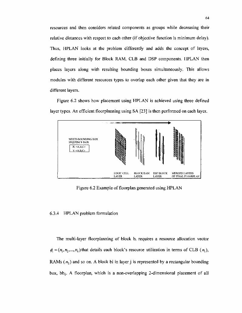
64
resources and then considers related components as groups while decreasing their
relative distances with respect to each other (if objective function is minimum delay).
Thus, HPLAN looks at the problem differently and adds the concept of layers,
defining three initially for Block RAM, CLB and DSP components. HPLAN then
places layers along with resulting bounding boxes simultaneously. This allows
modules with different resources types to overlap each other given that they are in
different layers.
Figure 6.2 shows how placement using HPLAN is achieved using three defined
layer types. An efficient floorplanning using SA [23] is then performed on each layer.
LOGIC CELL BLOCK RAM DSP BLOCK MERGED LAYERS LAYER LAYER LAYER OF FINAL FLOORPLAN
Figure 6.2 Example of floorplan generated using HPLAN
6.3.4 HPLAN problem formulation
The multi-layer floorplanning of block bj requires a resource allocation vector
$ =(«1,«2,...,«/t)that details each block's resource utilization in terms of CLB (n,),
RAMs (n2) and so on. A block bi in layer j is represented by a rectangular bounding
box, bby. A floorplan, which is a non-overlapping 2-dimensional placement of all
MULTI-BOUNDING BOX SEQUENCE PAIR
X: <A,B.C> Y: <A.B.C>

65
blocks B in the ith layer is represented by the set F -(fvf2,-,fk) • The criteria to
validate a floorplan are:
(a) F is free to overlap blocks in other layers but itself
(b) F fits inside the device physical boundaries
(c) F consume up to the maximum resource allocated to each layer
The problem statement is completed with the objective function for the placement
algorithm which is to find a feasible solution F to minimize the cost function:
C(F) = cx • area(F) + c2 • wirelength(F) + c3 • aspect ratio penalty'(F) +
c4 • bounding box_deviation(F)
For the first term area(F), the final area of the floorplan (F) is obtained by
multiplying the maximum height with the maximum width of all layers. The second
term, wirelength(F), is obtained using half-perimeter of bounding boxes through
each layer. For third term, aspect ratio penalty(F) is obtained from the difference
between the aspect ratio of floorplan F and the one of the device used. The final term
bounding box _deviation(F) is obtained from the displacement between boxes and
is used to bring them close to each other.
HPLAN also uses a notation to represent multiple floorplans for each layer. The
arranged enumeration gives information of the placement of modules of a particular
layer with respect to one another. The sequence pair for multiple bounding boxes,
commonly called multiBox Sequence Pair (BSP) is defined as follows:
BSPA = (<..., p,...,q,...>,<..., p,..., q,... >)
=>M>rfisleftofM„ Vj,\<j<k
BSPB = (<...,p,...,q,...>,<...,p,...,q,... >)
=> bb is above of bb, V/, 1 < j < k

66
The BSP criteria accordingly states that each bounding box of a layer is linked to all
others which belong to the same layer according to either BSPA or BSPB .
6.3.5 Comments
The methodology presented in [23] shows how to properly separate and place
heterogeneous blocks into large FPGA devices. The algorithm is effective with
disproportionate design. The objective function as well as the final placement
algorithm is chosen such that most designs are covered. Area and wirelength in
particular are used as cost function while SA is used for final block placement. To
support their claim, the author used as an example a design containing a Microblaze
processor with coprocessors for DES, CRC and FFT and was eventually targeted to a
Xilinx Virtex-4 FPGA. The placement algorithm writes a user-constraint file (UCF) at
the end of the process which gives the explicit location of each block.
In the context of a multiplier design with pipelining, the placement algorithm can
be further enhanced since the critical path of the design is known before-hand. Also,
the cost function can also include a power component which would make the new
placement algorithm aware of how power is affected if more logic cells are used. In
the remaining document, we explain modifications that are brought to [23] along with
a different final placement algorithm based on a greedy algorithm instead of SA, as
originally suggested by the authors.

67
6. 4 Relative Placement Macros
The Xilinx toolset [30] gives a convenient way of representing hardware structures
together with their physical, absolute or relative locations. Relationally Placed Macros
(RPM) [31] add location attributes along with hierarchical relationships to a structural
HDL model. Synthesis transfers that information to the netlist file which is then used
at the mapping stage. Most basic elements in the FPGA fabric can have a relative
location compared to an initial reference element. The attribute RLOC is used to
convey the placement information to the mapper. For example, in a VHDL design,
RLOC is defined as:
--DECLARATIVE PART
attribute RLOC : string;
-DECLARATIVE PART OF GENERATE
attribute RLOC of A C A 0 0 label is 'XmYn"
Figure 6.3 Usage of Relative Location in hardware descriptive language
As shown in Figure 6.3, ACA00 is an instance of component ACA (Arithmetic
Cell A), which is a module used in the proposed multiplier algorithm. RLOC also uses
the Cartesian coordinate system as the relative physical placement grid, which began
with Virtex-2 family of FPGA. The notation is Xm and Yn, where m and n are integer
values. The X and Y values are translated to absolute coordinates by the synthesizer
using the difference between RLOC and the reference element.
In Figure 6.4, Arrangement2, the RLOC notation is used to place up to four flip-
flops per CLB, accounting for half of its utilization. This is because RLOC works at

68
the slice level where each slice consists of two flip-flops [32]. A turn around is to
place the same RLOC for two components within the same hierarchy, thus forcing the
mapper to put two flip-flops in the same slice.
1 L _
LSLOC 1 rxoY2 1
1 1 1
J SLICE
1 1
TXOYO 1
1 1 1
J SLICE
CLB
LSLOC ' 1 rX0Y2 I
1 1
LSLOC 1 rxm 1
1 1 SLICE
LTELOC 1 novo 1
1 1
rra.BC 1 rxjYo I
1 1
SLICE
rsroc "1 fXOYO 1
1 1
rxiYo i
I i
SLICE
ARRANGEMENT 1 ARRANGEMENT 2
Figure 6.4 Internal logic slice arrangement using RLOC attribute
Along with specifying locations, components can also be grouped according to
rules. The keywords HSET, USET and HU_SET are used to create or modify
relationships among basic elements in a design. Elements under the same hierarchy
are by default labelled with auto-generated H_SET attributes, indicating that they
belong to one particular set and are hence related. Moreover, USET attributes have
an arbitrary but distinct name. Any component with same USET will belong to the
same group, irrespective of their design hierarchy. Finally, HUSET modifies the
HSET set attribute to allow arbitrary set names. The proposed partition algorithm
generates structural VHDL, hence implicitly enabling the use of HSET.
Figure 6.5 shows how RLOC organizes a design using either HSET or HUSET.
Component A and B inherit by default their parent "hset" name. This is different in
the second case (Hierarchy with HUSET), where HUSET is used in component C.
This forces the synthesizer to rename components in D and E with the arbitrary name
"TEMP".
IZZI
I I SLICE
LHEOC rX4YQ
1
LW-OC 1 ftcYO I 1 1
1 1
SLICE
CLB

69
TOP LEVEL TOP LEVEL
RLOC X0Y1
B
W B 1 H SET= B'htti
H SET= B?hs«
a m
}• COMPONENT 'A' INSTANTIATION
:HU_SF!feH TEMP •
RLOC :H SEI=
» • G •
E H • I •
HIERARCHY WITH H SET HIERARCHY WITH HU SET
Figure 6.5 Hierarchy representation using HSET and HU_SET
6. 5 Area, delay and Power Heuristics
6.5.1 Area
Area is bound to have a minimum value representing the sum of all slices used in
the hardware multiplier. In addition, pass-through look-up tables are used whenever
interconnect resources are exhausted as a consequence of highly congested regions. A
possible heuristic to the area problem is: Knowing in advance the area of high-
congestion and eventually adding slack space to accommodate for more routing
resources will decrease the amount of slices used as pass-through logic. Also,
predicting the amount of congestion and planning for additional area will increase the
chance of finding a solution while also reducing the placer run-time.
A block with high fan-in and fan-out is bound to have a highly congested region,
hence increasing area, delay and power. Blocks falling in this category should be
placed first. A possible heuristic to the second area problem is: Finding the maximum

70
cut between two vertices permits placement according to high fan-in, fan-out and
maximum delay.
6.5.2 Delay
Obtaining the critical path and therefore blocks that include it allows the algorithm
to place that block first, hence increasing likelihood of meeting timing constraints. A
possible heuristic to the delay problem is: Finding the longest combinational path in
part of the graph which covers a block yields an accurate estimation for delay and
allows high-priority placement for that block.
A loaded net will have buffers inserted automatically by the synthesis tool to
reduce delay. An optimum placement for the buffer would be one with minimum
length to all sinks, or more importantly, one that would not increase the worst case
delay. A possible heuristic for redundant buffer removal is: Select an edge with a
certain load, insert a new node (buffer) and place it so that the overall delay of the
system is unchanged.
6.5.3 Power
Minimizing area and interconnect length all have an indirect but positive effect in
power reduction. Using empirical data, the cost function for power will be obtained.

6. 6 Proposed Placement Algorithm
71
The partition algorithm for long-unsigned multiplication as presented in Chapter 5
is improved with a new placement algorithm that takes into consideration important
details of placement in FPGA technologies, such as a reduction in long-type
interconnect, removal of pass-through logic and placement according to critical
combinational path. Also, part of the new algorithm is based on work presented in
[23] and relates to placement of the blocks within the physical limit of the FPGA
device.
A generated multiplier design is initially updated with locality information, using
Xilinx PvLOC attributes. The partition algorithm defines two main arithmetic units,
Arithmetic Cell A (ACA) and Arithmetic Cell B (ACB) in addition to cascade register
(CR) blocks. The placement algorithm considers ACA, ACB and CR as atomic blocks
having predefined layouts which it then arranges optimally. Figure 6.6 shows the
improvement in delay and PAR runtime when using RLOC to create arithmetic cells.
The blocks ACA, ACB and CR are in O(L) area-wise and in O(l) delay-wise, where L
is the latency. The area is a function of latency only since for each increment in L, the
depth of the pipeline is increased by L while the datapath's width remains constantly
at either 17 or 34 bits. Delay of a block is also constant given that the distance
between pipelining columns is fixed and that the local interconnect is used as routing
resource.

72
ARITHMETIC CELL 'B ' (ACB)
ARITHMETIC CELL 'A' (ACA)
DSP48 SLICE
DELAY: 2.346nS(2.824nS) RUNTIME: 26S (34S)
Values in parenthesis are for un-placed macros
CASCADE REGISTER (CR)
111! III! 1111 111!
INPUT REGISTERS OUTPUT REGISTERS INPUT REGISTERS OUTPUT REGISTERS
1.220nS(2.462nS) ]min24S(2min20S)
1.006nS(1.336nS) 39S(39S)
All blocks are with latency of 4 registers
Figure 6.6 ACA, ACB, CR Macro blocks internal placement
6.6.1 Area constraints formulation
The proposed placement algorithm is partly based on the HPLAN heterogeneous
floorplanner [23]. HPLAN decomposes a complete system into basic primitives,
groups the primitives into different layers, adds bounding-box constraints at all layers
and finally produces a result by combining the layers if and only if:
(a) The resources needed do not exceed the total available in the FPGA.
(b) There are no collisions between bounding-boxes.
(c) All layers fit in their respective primitive sets.
The proposed placement algorithm restricts the HPLAN resource allocation vector
cj>. to primitives only used by the proposed partition multiplier algorithm, which are
DSP48 (ni) and FLIP-FLOPS (n2), thus <D, ={«,,/%}. Since |<D,| = 2, the number of layers
needed is also two. The set of high level blocks used is defined as
H = {ACA,ACB,CR,DSP48}. The generated floorplan F is the aggregate of f.,f. being

73
the non-overlapping placement of o, in each layer. The problem is simplified as only
elements in H have to be placed. It can be proven that elements have to be mutually
exclusive in order to satisfy the second HPLAN criteria. The set of all components
used to build the large-integer multiplier is B={ACA0, ACA),..., ACB0, ACBi,...,
CR0, CR,,..., DSP480, DSP48,,...}.
We also define the cardinality of B as BC= \B\ . The bounding box for each element
in B is bby where i={ 1,2} and j={l,...,Bc}. As each ACA block consists of 2 DSP48
blocks, bbij(ACA)=2. An ACB block contains a 17bits adder with optional pipeline
registers hence bbij(ACB)=l. Lastly, cascade register CR consists of only flip-flops
thus bbij(CR)=0. Figure 6.7 depicts the physical layout of arithmetic blocks and gives
worst case scenarios for the heights and widths. We can hence find the flip-flops
count, which is represented by n2 and obtained from the following equations:
bb2j {A CA) = 34(1 + xL + 2y + 2L) Eq. 16
bb2j(ACB)L° = l7(L0 + Ll) Eq. 17
bb2j(CR)L = 17L Eq. 18
where L=latency, x=register-e enable {0, 1}, y=output register enable {0, 1}, Lo=input
register latency, Li=output register latency. This completes the analysis for HPLAN.
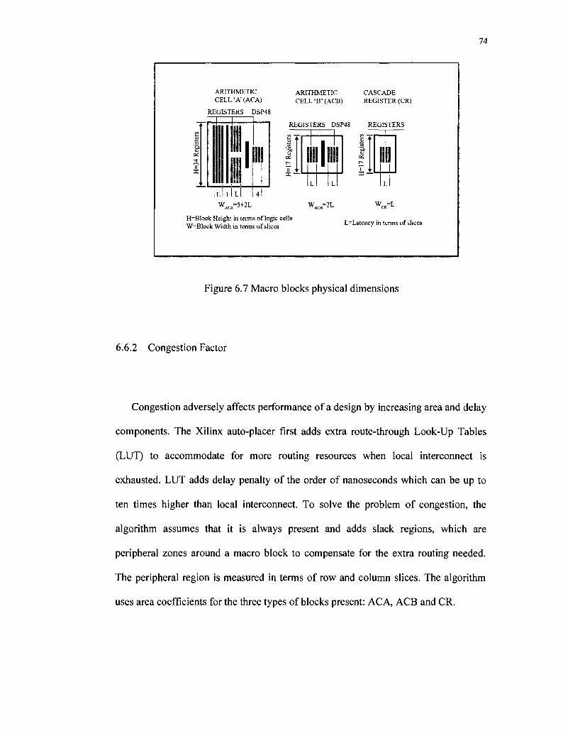
74
ARITHMETIC CELL 'A' (ACA)
REGISTERS DSP48
H=3
4 R
egis
ters
I |ll L 1 I Li 4
ARITHMETIC CELL 'B ' (ACB)
CASCADE REGISTER (CR)
REGISTERS DSP48 REGISTERS
=17
Reg
iste
r <
>
~
>l> L L
1" 7 .. 3d —
II L
H=Block Height in terms of logic cells W=Block Width in terms of slices
W„=L
L=Latency in terms of slices
Figure 6.7 Macro blocks physical dimensions
6.6.2 Congestion Factor
Congestion adversely affects performance of a design by increasing area and delay
components. The Xilinx auto-placer first adds extra route-through Look-Up Tables
(LUT) to accommodate for more routing resources when local interconnect is
exhausted. LUT adds delay penalty of the order of nanoseconds which can be up to
ten times higher than local interconnect. To solve the problem of congestion, the
algorithm assumes that it is always present and adds slack regions, which are
peripheral zones around a macro block to compensate for the extra routing needed.
The peripheral region is measured in terms of row and column slices. The algorithm
uses area coefficients for the three types of blocks present: ACA, ACB and CR.

6.6.3 Objective function
75
The aim of the placement algorithm is to minimize area, delay, power and
congestion. The general objective function is: F=CA-FA+CD-FD+CP.FP where CA is the
cost factor for area, Co is the cost factor for delay and CP is the cost factor for power.
In order to achieve a monotonous function, F is modified with the terms for power and
area combined into a single coefficient. This is true, considering that as area increases,
so is the amount of interconnect and hence capacitance. Since p = cv2f where C is the
node capacitance, V is the voltage and f frequency of operation, power relates to area
but not linearly. Furthermore, the congestion coefficient is added to the objective
function. The new FA is now CAI=CA+CP+CC, where Cc is the congestion coefficient
while the refined objective function is:
F=C F+C F 1 ^Al l A ^^D l D
6.6 A Graph theory
Figure 6.8 shows an equivalent graph for a 51 bits input multiplier. The input is
broken down into three 17bits segments that feed the DSP48 multipliers Mo to M2. All
blocks except CRX are based on DSP48 cores. According to HPLAN, layer ni will
contain DSP48 cores only while n2 will have registers. Since DSP48s are further
constrained to specific columns in the FPGA fabric, they are given the highest
placement priority over registers (n2) which are mapped to regular logic cells. The
algorithm also determines the critical path of the circuit and the fan-out for each
macro block, both of which are used as criteria in the algorithm. To simplify the
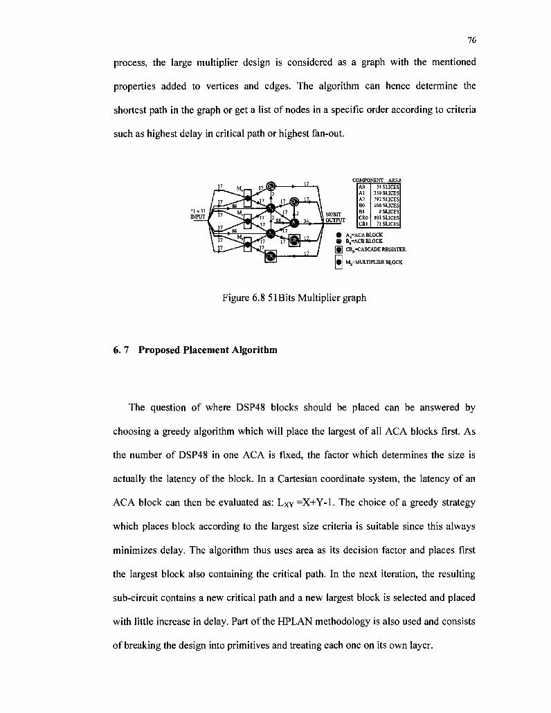
76
process, the large multiplier design is considered as a graph with the mentioned
properties added to vertices and edges. The algorithm can hence determine the
shortest path in the graph or get a list of nodes in a specific order according to criteria
such as highest delay in critical path or highest fan-out.
COMPONENT AREA AO Al A2 BO Bl CRO CR1
54 SLICES 259 SLICES 292 SLICES 106 SLICES
9 SLICES 103 SLICES 71 SUCES
• A ^ A C A BLOCK % BS=ACB BLOCK
[ # ] CRX=CASCADE REGISTER
B M ^MULTIPLIER BLOCK
Figure 6.8 51Bits Multiplier graph
6. 7 Proposed Placement Algorithm
The question of where DSP48 blocks should be placed can be answered by
choosing a greedy algorithm which will place the largest of all ACA blocks first. As
the number of DSP48 in one ACA is fixed, the factor which determines the size is
actually the latency of the block. In a Cartesian coordinate system, the latency of an
ACA block can then be evaluated as: LXY=X+Y-1. The choice of a greedy strategy
which places block according to the largest size criteria is suitable since this always
minimizes delay. The algorithm thus uses area as its decision factor and places first
the largest block also containing the critical path. In the next iteration, the resulting
sub-circuit contains a new critical path and a new largest block is selected and placed
with little increase in delay. Part of the HPLAN methodology is also used and consists
of breaking the design into primitives and treating each one on its own layer.
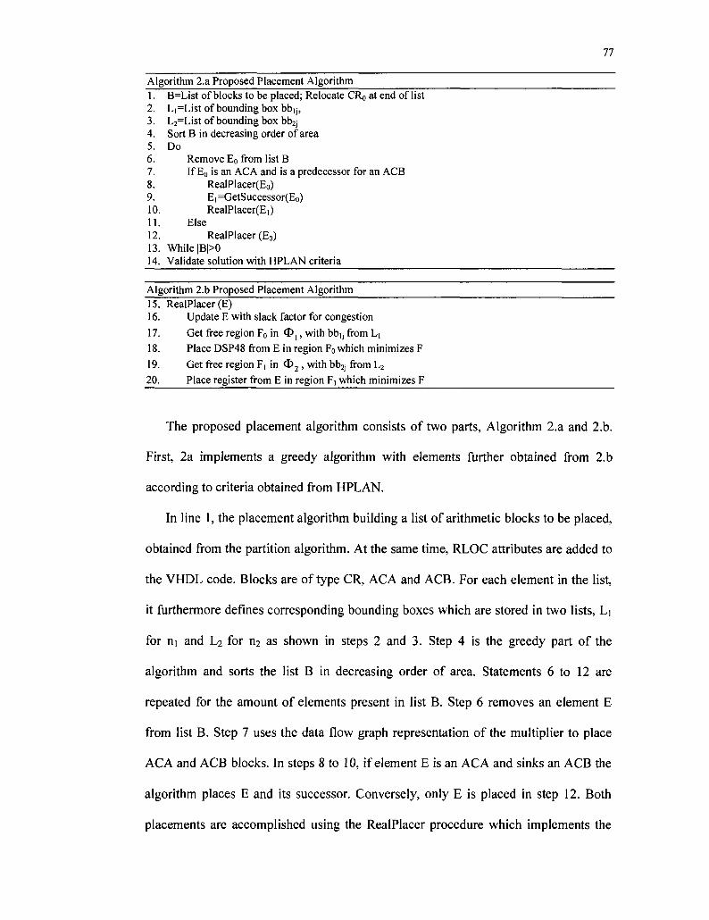
77
Algorithm 2.a Proposed Placement Algorithm 1. B=List of blocks to be placed; Relocate CRQ at end of list 2. L,=List of bounding box bbij, 3. L2=List of bounding box bb2j
4. Sort B in decreasing order of area 5. Do 6. Remove E0 from list B 7. If E0 is an ACA and is a predecessor for an ACB 8. RealPlacer(Eo) 9. E,=GetSuccessor(Eo) 10. RealPlacer(E,) 11. Else 12. RealPlacer (E0) 13. While |B|>0 14. Validate solution with HPLAN criteria
Algorithm 2.b Proposed Placement Algorithm 15. RealPlacer (E) 16. Update E with slack factor for congestion 17. Get free region F0 in <!>,, with bb,j from Li 18. Place DSP48 from E in region F0 which minimizes F 19. Get free region F] in <&2 , with bb2j from L2
20. Place register from E in region F, which minimizes F
The proposed placement algorithm consists of two parts, Algorithm 2.a and 2.b.
First, 2a implements a greedy algorithm with elements further obtained from 2.b
according to criteria obtained from HPLAN.
In line 1, the placement algorithm building a list of arithmetic blocks to be placed,
obtained from the partition algorithm. At the same time, RLOC attributes are added to
the VHDL code. Blocks are of type CR, ACA and ACB. For each element in the list,
it furthermore defines corresponding bounding boxes which are stored in two lists, L]
for ni and L2 for n2 as shown in steps 2 and 3. Step 4 is the greedy part of the
algorithm and sorts the list B in decreasing order of area. Statements 6 to 12 are
repeated for the amount of elements present in list B. Step 6 removes an element E
from list B. Step 7 uses the data flow graph representation of the multiplier to place
ACA and ACB blocks. In steps 8 to 10, if element E is an ACA and sinks an ACB the
algorithm places E and its successor. Conversely, only E is placed in step 12. Both
placements are accomplished using the RealPlacer procedure which implements the

78
HPLAN methodology with F as objective function. Operations are executed in 0(1)
except for sorting which takes O(nlogn) when implemented using Quicksort while
the loop at line 5 is in O(n).
The last step is to verify if all conditions necessary for HPLAN are satisfied,
namely, if all blocks located in different layers are mutually exclusive, that they do
not lie outside of the FPGA boundaries and that primitives used fit inside their
allocated regions. The placement algorithm can then be applied to the graph in Figure
6.8 and results in B={A2, A\, Bo, CRo, CRi, Ao, Bi}. At first, E=A2 and on the initial
iteration, A2 and Bi are placed. The second iteration will then place Ai and Bo along
with CRi which is placed adjacently to Ai. Multipliers M2, Mi and Mo are next placed
while CRo is placed at the end. The RealPlacer procedure uses a seed location to
indicate the initial placement of the first block to be placed (A2). By default, the seed
locates A2 at the bottom of the FPGA die and augments the Y coordinate for each
pass.
Figure 6.9 illustrates the resulting layout for a 51 bits multiplier with the proposed
placement algorithm. Initially, block A2 is placed using HPLAN using an initial seed
having the coordinate of the first DSP48 in the column. The next step iteratively
places Bi, Ai and B0, A0, CRi, M2, Mi, M0 and finally CRo. There can be other
solutions for the same design if different seeds are used. Since the critical path is
minimized, the difference in performance for other placements is negligible.

79
0 A,=ACA BLOCK g B„=ACB BLOCK g g CR^ASCADE REGISTER
'9I M -̂MULTIPLIER BLOCK
Figure 6.9 51 Bits multiplier physical layout graph, as generated by proposed partition
algorithm
6.8 Results
Performance results in terms of area and delay are given below. Delay is
furthermore broken down in terms of interconnect and combinational path delay, the
latter including both gate and interconnect delay. Efficiency of the proposed
placement algorithm is also measured quantitatively with the run-time of the place-
and-route tool for different input sizes. In the graphs, "Tool placed" represents cases
where the placement algorithm is not used and with values that were initially obtained
using only the provided CAD placement algorithm.
The placement algorithm was modified for the tests, with the addition of a
threshold level that stopped execution if the size of the current block placed was less

80
than a certain number. This allowed the place-and-route tool to take over and do a
regular placement. Consequently, this modification prevented the use of large
segmented nets which appeared at the end in the proposed placement algorithm, for
very large input length.
6.8.1 Combinational path delay
Combinational path delay of various multipliers placed with the proposed
placement algorithm is shown in Figure 6.10. Since the gate delay is constant as stated
in Eq. 14, the net combinational delay depends solely on interconnect delay. The
figure shows that for widths between approximately 32bits and 15 lbits (Region of
interest), the proposed placement algorithm generates solutions that outperform those
obtained from the alternative placement tool.
JS
Q
H 3
I 2
c E
8 1
<C^s
'^MW^MMW^;W^^ • - •
_ _ _ - - - " "
Raced
Raced w ith area threshold Interconnect delay (Raced)
50 100 150
Size of Operands (bits)
200 250
Figure 6.10 Combinational path delay for designs initially placed using proposed
placement algorithm

81
Figure 6.11 shows how interconnect delay progresses with changing width size.
Using the proposed placement algorithm with an area threshold of 1500 registers
minimizes the effect of wire segmentation present in the FPGA interconnect.
Consequently, the result is improved until approximately 151bits, where curves for
"Placed with area threshold" and "Tool placed" intersect each other.
3.5
3
2.5
2
1.5
1
0.5
0
Raced
Placed with area threshold j
Tool placed
.S
100 150
Size of Operands (bits)
200 250
Figure 6.11 Interconnect delay in placed multiplier designs
6.8.2 Virtex-4 logic slice utilization for placed design
The proposed placement algorithm treats ACA, ACB and CR blocks as atomic
elements without merging them. The mapping part of the implementation flow is not
as effective in removing duplicate logic as it could be. Hence, an increase in terms of
logic cells used is noted and shown in Figure 6.12. To offset this, the graph algorithm
used should be modified to take into accounts inputs and latency registers that have

82
similar delays and further combine them together. Then, outputs from these register
banks would be used to drive ACA and ACB blocks.
60000 -r
50000 -
| 40000 -
| 30000 -
•5 _§ 20000 -E z
10000 -
0 -•
0 20 40 60 80 100 120 140
Size of Operands (bits)
Figure 6.12 Logic slice utilization for placed multipliers designs
6.8.3 Place-and-route tool runtime
As shown in Figure 6.13, the proposed placement algorithm makes it easier for the
place-and-route (PAR) algorithm built in the design tool to execute. Consequently, the
proposed algorithm gives a gain in performance of approximately 9% when compared
to running the PAR without the initial placement step.

83
3
tr •2 o a. -a c ro <D o iS Q .
2000-
1500 -
1000 -
500
0
Tool placed
Placed
.''
•^1/
/ /
* /
.-•
-' /
20 40 60 80
Size of Operands (bits)
100 120 140
Figure 6.13 Place-and-route run-time for different multiplier designs
6.9 Summary
The placement algorithm presented in this chapter increases the multiplier's
timing performance by as much as 20% in the case of an input width of 64bits. The
algorithm itself will improve on an unplaced design for input sizes in the range of
32bits to 15 lbits. Since the cost function used and hence heuristics employed consider
minimizing delay as the main objective, area utilization suffers to a certain extent. In
this view, the proposed algorithm can be enhanced by using a refined graph model
that would instead treat AC A, ACB and CR block as non-atomic and remove
redundant elements. Once done, the algorithm would then regroup the basic blocks
and continue with steps outlined. Finally, the run-time for implementing large
multiplier designs is also reduced.

84
7 VERIFICATION STRATEGY
The final stage in the design of the partition and placement algorithm is to verify
the proper operation of solutions generated. The objective of the first algorithm is to
break down a large-input unsigned multiplier design using smaller 17bits ones, with
which the actual multiplication operations are performed. Also, 34bits adders are used
to sum partial products into the final result. The partition algorithm makes use of
custom-made discrete blocks, ACA, ACB and CR, where each has specific behaviours
when subjected to particular input combinations. The large-input multiplier uses the
forth-mentioned modules, interconnected together to form a working entity.
Since the generated solution can be viewed as a hierarchy of components as shown
in Figure 7.1, the strategy adopted was to test the functionality of each block at each
level and then test the multiplier entirely. Initially, DSP48 blocks and register
components were assumed to be working properly. This represents the lowest level of
component and is provided by the FPGA vendor, while VHDL models were also
available. They have been already tested and are assumed to be trustworthy.
TESTING NEEDED
TESTING NEEDED
TRUSTWORTHY LEVEL MODELS SUPPLIED BY FPGA MANUFACTURER
TESTING STRATEGY
VHDL TESTBENCH
VHDL TESTBENCH
NO TESTING
Figure 7.1 Testing hierarchy for multiplier partition algorithm

7. 1 Behavioural Verification
85
ACA, ACB and CR are tested with VHDL testbenches and the test flow is shown
in Figure 7.2. Stimulus signals are first applied at the multiplier's inputs while having
its outputs recorded. The behaviour is then compared to expected results as obtained
from Eq. 1 and Eq. 2. Finally, the large integer multiplier is tested at the top-level,
with random stimulus given using a VHDL testbench. The behaviour is again
recorded and compared against the expected result obtained from the multiplier
operator provided by the VHDL unsigned library.
UNIT UNDER TEST (UUT)
RTL VHDL MODEL
BIT COMPARE TEST
BEHAVIORAL VHDL MODEL
POST-SYNTHESIS MODEL AND SIMULATION
VHDL TESTBENCH
XILINX VHDL SYNTHESIZER
VHDL NETLIST
VHDL MODEL MODIFICATION
MODELSLM VHDL SLMULATOR
Figure 7.2 Test setup for multiplier designs
Figure 7.2 shows one possible test procedure. This was used for testing all the
basic blocks and the final multiplier designs. Furthermore, timing analysis was done

86
using this set-up by replacing UUT with the gate-level HDL model containing the
appropriate delays.
7. 2 Timing Analysis
Timing analysis and simulation consist of running the place-and-route (PAR) step
of the CAD tool. This will generate a structural model containing delays along with a
timing report from which information such as critical path delay and maximum
frequency of operation are obtained. Timing simulation catches timing errors such as
setup and hold violations, which are not present in the post-synthesis model. The
report also provided data for the graphs presented in Chapters 5. The PAR step
required a constraint file containing the targeted frequency of operation.
7. 3 Placement Algorithm Testing
The placement algorithm decreases combinational delay while removing pass-
through gates which are look-up tables used as interconnect. Placement information
was added either in the VHDL file description or in the constraint file. Since the basic
arithmetic blocks and connections are unchanged, no simulation was done in the
placement phase. Data for critical path delay, area utilization and maximum frequency
of operation were collected from report files and used in Chapter 6.

87
8 CONCLUSION AND FUTURE WORK
This thesis presented algorithms that increase the efficiency of DSP48 blocks so as
to realize large-integer unsigned multiplication.
8.1 Partition Algorithm
The generic algorithm presented by Shuli Gao et al. [4] paved the way for the
proposed partition algorithm. As such, the research involved finding a suitable
mapping that would allow an even higher performance for these classes of hardware
parallel multipliers. It was noted that high timing performance could be further
enhanced by the use of pipelining as the DSP48 block reaches maximum frequency of
operation under specific condition. The suggested partition method and resulting
algorithm [5] minimize gate delay, as shown in Figure 5.13 Routing performance
degradation for higher word length. The method makes use of pipelining registers
present in any DSP48 block.
8. 2 Placement Algorithm
Research in the area of floorplanning as obtained from a survey of placement
algorithms gave more insight on newer generations of algorithms and heuristics for
FPGA technologies, particularly ones that are related to heterogeneous placers. By

88
positioning groups of related logic units together according to certain rules,
interconnect delay is hence mitigated to a certain extent. The most pertinent method
for heterogeneous floorplanners was proposed by Love Singhal et al. [23], which
attempts to solve the problem by assigning resources to layers and applying the
placement algorithm on these layers.
Our placement algorithm tries to reduce interconnect delay by placing large
arithmetic units first while also placing components related to the critical path [6].
Resource allocation is performed using HPLAN [23]. The proposed concept is based
on the greedy model which considers local optimum solutions. The method also
minimizes congestion by giving slack space around the basic building blocks of the
multiplier. It was shown that when using this methodology, interconnect delay and
consequently maximum frequency of operation for very large multiplier circuits were
enhanced. Use of the placement algorithm is of course optional but should be
employed if the highest timing performance is needed.
S. 3 Conclusion
Presented here are two algorithms that will help in designing multiplier circuits
implemented in the Virtex-4 family of FPGA. Performance measure, in terms of Area-
Delay product for both fully-pipelined and non-pipelined versions is provided to give
an idea of what to expect for a certain input length. Consequently, the designer has the
choice of picking the appropriate large-integer multiplier design for the best cost
function of the project.

8. 4 Future Work
89
The algorithms presented in this thesis are not perfect. They were designed to
optimize speed and minimize both interconnect and gate delay. Area used up by the
pipelining registers can be further reduced when the placement algorithm is used.
Using data flow graphs, a better algorithm can be obtained that would remove
equivalent registers and hence decrease area utilization.
The given algorithms can be easily adapted to newer FPGA such as the Virtex-5,
which possesses better DSP blocks. Since the designing approach of the partition
algorithm is modular, one would just need to update ACA, ACB and CR with newer
equivalent models.

90
REFERENCES
[I] Charles Poynton, "Digital Video and HDTV Algorithms and Interfaces", pp. 127.
[2] Uwe Meyer-Baese, "Digital Signal Processing with FPGA", 1st Edition, pp. 248.
[3] Uwe Meyer-Baese, "Digital Signal Processing with FPGA", 1st Edition, pp. 232.
[4] S.Gao, N.Chabini, D.Al-Khalili, and P.Langlois, "Efficient Realization of Large
Integer Multipliers and Squarers", Circuits and Systems, 2006 IEEE North-East
Workshop.
[5] J.L.Athow, AJ.Al-Khalili, "Implementation of Large-Integer Hardware Multiplier
in Xilinx FPGA", IEEE International Conference on Electronics, Circuits and
Systems, 2008.
[6] J.L.Athow, A.J.Al-Khalili, "Placement Algorithm For Multiplier-Based Fpga
Circuits", IEEE International Conference on Microelectronics, 2008.
[7] J.P.Deschamps, G.J.A.Bioul, G.D.Sutter, "Synthesis of Arithmetic Circuits", 1st
Edition, pp. 369.
[8] B. Payette, "Color Space Converter: R'G'B to Y'CbCr", Xilinx, XAPP637, 2002.
[9] K. Chapman, "Constant Coefficient Multipliers for the XC4000E", Xilinx,
XAPP054, 1996.
[10] K. Chapman, "Fast Integer Multipliers Fit in FPGAs" , EDN, vol. 39, no. 10,
1994, pp. 80.
[II] Jean-Pierre / Bioul, Gery J. A. / Sutter, Gustavo D. Deschamps "Synthesis of
Arithmetic Circuits: FPGA, ASIC and Embedded Systems" .

91
[12] S. Elzinga, J. Lin, V. Singhal, "Design Tips for HDL Implementation of
Arithmetic Functions", XAPP215, June 2000, pp. 11.
[13] Virtex 2.5V Field Programmable Gate Arrays, pp. 7.
[14] A. Cosoroaba, F. Rivoallon, "Achieving Higher System Performance with the
Virtex-5 Family of FPGAs", Xilinx WP245, pp. 5, July 2006
[15] B. New, Xilinx, "Using the Dedicated Carry Logic in XC4000E", XAPP013,
July 1996, pp. 4.
[16] B. New, Xilinx, "Using the Dedicated Carry Logic in XC4000E", XAPP013,
July 1996, pp. 10.
[17] Xilinx "XtremeDSP for Virtex-4 FPGA User Guide", UG073, October 2007,
Figure 1-3, pp. 20.
[18] Xilinx "XtremeDSP for Virtex-4 FPGA User Guide", UG073, October 2007,
Table 1-6, pp. 30.
[19] Xilinx "XtremeDSP for Virtex-4 FPGA User Guide", UG073, October 2007,
Table 1-4, Table 1-5, pp. 29.
[20] Xilinx "XtremeDSP for Virtex-4 FPGA User Guide", UG073, October 2007,
Table 1-8, pp. 34.
[21] Xilinx, "Virtex-II Platform FPGA Detailed Description", DS031-2, Module 2,
pp. 35, December 2002.
[22] S.M. Sait, H.Youssef, "VLSI Physical Design Automation" McGraw Hill
Book Company, 1995, pp. 23.
[23] Love Singhal, Elaheh Bozorgzadeh, "Heterogeneous Floorplanner for FPGA",
IEEE FCCM07.

92
[24] S. Kirkpatric, CD. Gelatt, MP. Vecchi, "Optimization by simulated
annealing", Science, vol. 220, no. 4598, pp. 671-680, May 1983.
[25] H. Krupnova, C. Rabeaoro, G. Saucier, "Synthesis and Floorplanning for
Large Hierarchical FPGAs", FPGAACM FPGA97.
[26] J. Stohmann, K. Harbich, M. Olbrich, E. Barke, "An Optimized Design Flow
for Fast FPGA-Based Rapid Prototyping", Institute of Microelectronic Systems,
University of Hanover, Callinstr. 34, D-30167 Hanover, Germany.
[27] J.M. Emmert, D. Bhatia, "A Methodology for Fast FPGA Floorplanning",
Proc. FPL, 1998, pp. 129-138.
[28] C. Ababei, Yan Feng, B. Goplen, H. Mogal, Tianpei Zhang, K. Bazargan, S.
Sapatnekar, "Placement and Routing in 3D Integrated Circuits", IEEE CASS05.
[29] L. Cheng, M.D.F Wong, "Floorplan Design for Multi-Million Gate FPGAs",
ACM ICCAD, pp. 292-299, 2004.
[30] Xilinx ISE 8.2 design tool suite, 2006
[31 ] Paul Glover, Steve Elzinga, "Relational^ Placed Macros", Xilinx WP329, Jan
2008
[32] Xilinx "Virtex-4 User Guide", UG070, August 2007, pp. 182
[33] Xilinx "XtremeDSP for Virtex-4 FPGA User Guide", UG073, October 2007,
Table 1-3, pp. 22-23.
[34] Xilinx "XtremeDSP for Virtex-4 FPGA User Guide", UG073, October 2007,
pp. 19.
[35] Xilinx FPGA Editor, Release 8.2.03i, 2006
[36] Xilinx XPower, Release 8.2.03i, 2006
93
APPENDIX A, VHDL MODELS
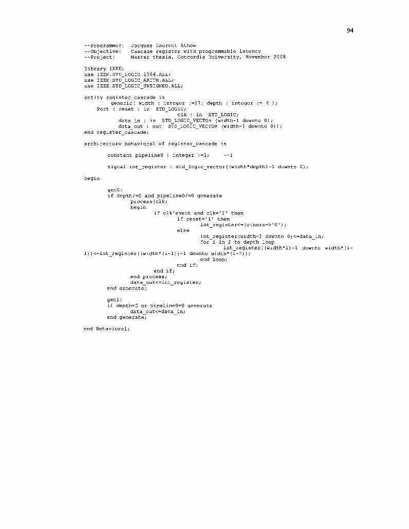
--Programmer: Jacques Laurent Athow --Objective: Cascade register with programmable latency —Project: Master thesis, Concordia University, November 2008
library IEEE; use IEEE.STD_LOGIC_1164.ALL; use IEEE.STD_LOGIC_ARITH.ALL; use IEEE.STD_LOGIC_UNSIGNED.ALL;
entity register_cascade is generic( width : integer :=17; depth : integer := 4 );
Port ( reset : in STD_LOGIC; elk : in STD_LOGIC;
data_in : in STD_LOGIC_VECTOR (width-1 downto 0); data_out : out STD_LOGIC_VECTOR (width-1 downto 0));
end register_cascade;
architecture Behavioral of register_cascade is
constant pipelineO : integer :=1; — 1
signal int_register : std_logic_vector((width*depth)-1 downto 0);
begin
genO: if depth/=0 and pipelineO/=0 generate
process(elk) begin
if elk'event and clk='l' then if reset='l' then
int_register<=(others=>'0'); else
int_register(width-1 downto 0)<=data_in; for i in 2 to depth loop
int_register((width*i)-1 downto 1))<=int_register((width*(i-1))-l downto width*(i-2));
end loop; end if;
end if; end process; data_out<=int_register;
end generate;
genl: if depth=0 or pipeline0=0 generate
data_out<=data_in; end generate;
end Behavioral;

—Programmer: Jacques Laurent Athow —Objective: Wrapper for DSP48 block, part of ACA —Project: Master thesis, Concordia University, November 2008
library IEEE; use IEEE.STD_LOGIC_1164.ALL; use IEEE.STD_LOGIC_ARITH.ALL; use IEEE.STD_LOGIC_UNSIGNED.ALL;
library UNISIM; use UNISIM.VComponents.all;
entity dsp48reg_wrapper is —generic ( bcin_en
Port ( elk : reset cin : din_a din_b din_c din_d din e
_ boolean ); in STD_LOGIC; : in STD_LOGIC; in STD_LOGIC; : in STD_LOGIC_VECTOR (16 downto 0)
STD_LOGIC_VECTOR (16 downto 0) STD_LOGIC_VECTOR (16 downto 0) STD_LOGIC_VECTOR (16 downto 0) STD LOGIC VECTOR (33 downto 0)
in in in in
bcin : in std_logic_vector(17 downto 0) ; bcout : out std_logic_vector(17 downto 0);
result : out STD_LOGIC_VECTOR (35 downto 0)); end dsp48reg_wrapper;
architecture Behavioral of dsp4 8reg_wrapper is
constant pipelineO constant pipelinel
integer integer
:=1; :=2;
— 1 —2
signal int_al, int_bl, int_a0, int_b0 : std_logic_vector(17 downto 0), signal int_cl, int_c0 : std_logic_vector(47 downto 0); signal int_p0, int_p : std_logic_vector(47 downto 0); signal int_res : std_logic_vector(47 downto 0); signal int_reg_din_e : std_logic_vector(33 downto 0); signal int_carry0, int_carryl : std_logic;
attribute RLOC : string; —attribute RLOC of DSP48_inst_slice2: label is "X0Y0"; —attribute RLOC of DSP48 inst slicel: label is "X0Y1";
begin
int_p0<=(others=>'0'); int_a0<='0'£din_a; int_b0<='0'Sdin_b; int_al<='0'sdin_c; int_bl<='0'&din_d; int_cO<=b"00_0000_0000_0000"sint_reg_din_e;
genO: if pipeline0=l generate process(clk)begin
if elk'event and clk='l' then if reset='l' then
int_reg_din_e<=(others=>'0') ; int_carry0<='0';
else int_reg_din_e<=din_e; int_carry0<=cin;
end if; end if;
end process; end generate;
genl: if pipeline0=0 generate int_reg_din_e<=din_e; int_carry0<=cin;
end generate;
DSP48_inst_slice2 generic map (
AREG => pipelineO, BREG => pipelineO,
DSP48
- Number of pipeline registers on the A input, 0, 1 - Number of pipeline registers on the B input, 0, 1
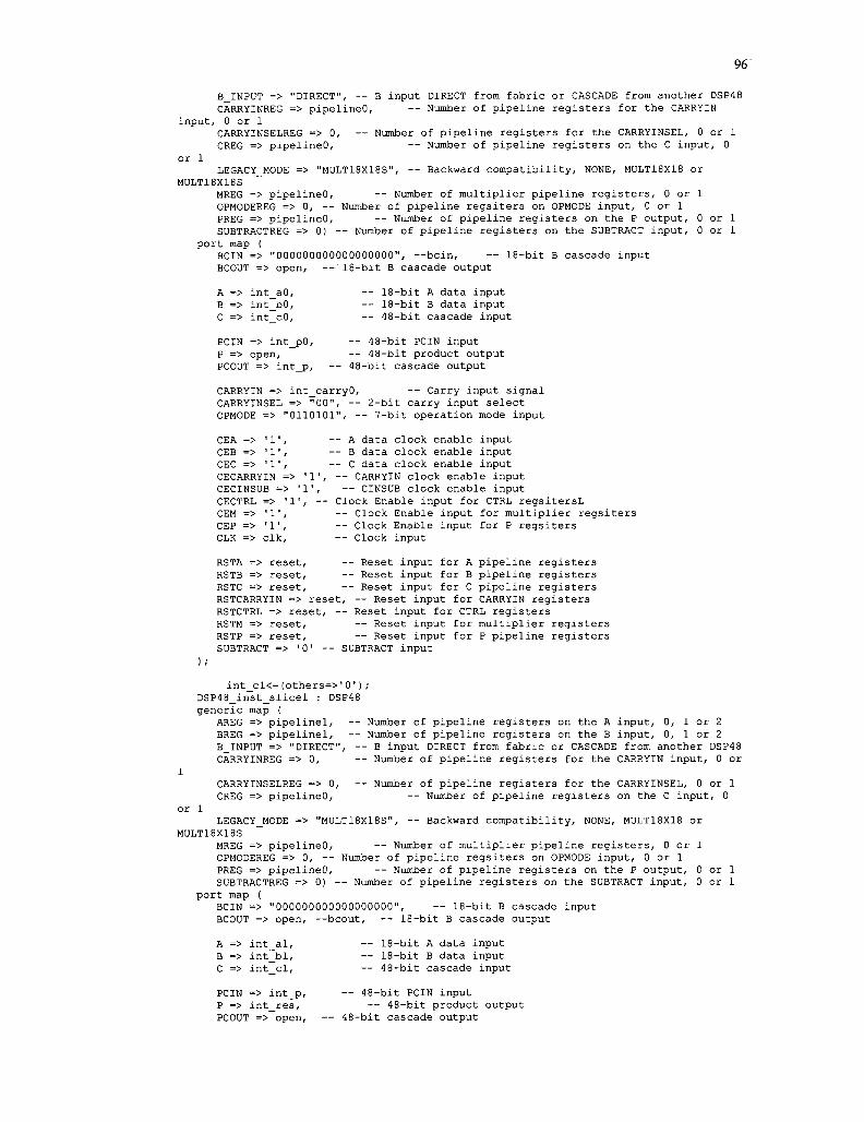
96
input
or 1
B_INPUT => "DIRECT", — B input DIRECT from fabric or CASCADE from another DSP48 CARRYINREG => pipelineO, — Number of pipeline registers for the CARRYIN 0 or 1
CARRYINSELREG => 0, — Number of pipeline registers for the CARRYINSEL, 0 or 1 CREG => pipelineO, -- Number of pipeline registers on the C input, 0
LEGACY_MODE => "MULT18X18S", — Backward compatibility, NONE, MULT18X18 or MULT18X18S
MREG => pipelineO, — Number of multiplier pipeline registers, 0 or 1 OPMODEREG => 0, — Number of pipeline regsiters on OPMODE input, 0 or 1 PREG => pipelineO, — Number of pipeline registers on the P output, 0 SUBTRACTREG => 0) — Number of pipeline registers on the SUBTRACT input, 0
port map ( BCIN => "000000000000000000", —bcin, — 18-bit B cascade input BCOUT => open, — 18-bit B cascade output
A => int_a0, B => int_b0, C => int c0,
18-bit A data input 18-bit B data input 48-bit cascade input
PCIN => int_p0, P => open, PCOUT => int_p,
— 48-bit PCIN input — 48-bit product output 48-bit cascade output
CARRYIN => int_carryO, -- Carry input signal CARRYINSEL => "00", — 2-bit carry input select OPMODE => "0110101", — 7-bit operation mode input
CEA => '1', — A data clock enable input CEB =>'!', — B data clock enable input CEC => '1', — C data clock enable input CECARRYIN => '1', — CARRYIN clock enable input CECINSUB => '1', — CINSUB clock enable input CECTRL => '1', — Clock Enable input for CTRL regsitersL CEM => '1', — Clock Enable input for multiplier regsiters CEP => '1', -- Clock Enable input for P regsiters CLK => elk, — Clock input
RSTA => reset, — Reset input for A pipeline registers RSTB => reset, — Reset input for B pipeline registers RSTC => reset, — Reset input for C pipeline registers RSTCARRYIN => reset, — Reset input for CARRYIN registers RSTCTRL => reset, — Reset input for CTRL registers RSTM => reset, — Reset input for multiplier registers RSTP => reset, — Reset input for P pipeline registers SUBTRACT => '0' — SUBTRACT input
),
int_cl<=(others=>'0'); DSP48_inst_slicel : DSP48 generic map (
AREG => pipelinel, BREG => pipelinel, B_INPUT => "DIRECT CARRYINREG => 0,
— Number of pipeline registers on the A input, 0, 1 or 2 — Number of pipeline registers on the B input, 0, 1 or 2 — B input DIRECT from fabric or CASCADE from another DSP48 — Number of pipeline registers for the CARRYIN input, 0 or
CARRYINSELREG => 0, CREG => pipelineO,
Number of pipeline registers for the CARRYINSEL, 0 or 1 — Number of pipeline registers on the C input, 0
or 1 LEGACY_MODE => "MULT18X18S", — Backward compatibility, NONE, MULT18X18 or
MULT18X18S MREG => pipelineO, — Number of multiplier pipeline registers, 0 or 1 OPMODEREG => 0, — Number of pipeline regsiters on OPMODE input, 0 or 1 PREG => pipelineO, — Number of pipeline registers on the P output, 0 or 1 SUBTRACTREG => 0) — Number of pipeline registers on the SUBTRACT input, 0 or 1
port map ( BCIN => "000000000000000000", — 18-bit B cascade input BCOUT => open, —bcout, — 18-bit B cascade output
A => int_al, B => int_bl, C => int cl,
— 18-bit A data input — 18-bit B data input — 48-bit cascade input
PCIN => int_p, — 48-bit PCIN input p => int_res, — 48-bit product output PCOUT => open, — 48-bit cascade output

97
CARRYIN => '0', CARRYINSEL => "00", OPMODE => "0010101",
— Carry input signal — 2-bit carry input select — 7-bit operation mode input
CEA => ' 1', — A data clock enable input CEB => ' 1', — B data clock enable input CEC => ' 1', — C data clock enable input CECARRYIN => '1', — CARRYIN clock enable input CECINSUB => '1', — CINSUB clock enable input CECTRL => '1', — Clock Enable input for CTRL regsitersL CEM => '1', — Clock Enable input for multiplier regsiters CEP => '1', — Clock Enable input for P regsiters CLK => elk, — Clock input
RSTA => reset, — Reset input for A pipeline registers RSTB => reset, — Reset input for B pipeline registers RSTC => reset, — Reset input for C pipeline registers RSTCARRYIN => reset, — Reset input for CARRYIN registers RSTCTRL => reset, — Reset input for CTRL registers RSTM => reset, -- Reset input for multiplier registers RSTP => reset, — Reset input for P pipeline registers SUBTRACT => '0' — SUBTRACT input
result<=int res (35 downto 0),
end Behavioral;
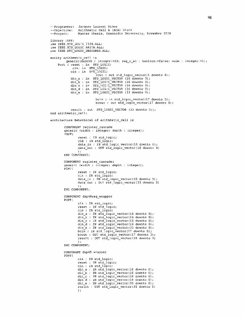
—Programmer: Jacques Laurent Athow —Objective: Arithmetic Cell A (ACA) block —Project: Master thesis, Concordia University, November 2008
library IEEE; use IEEE.STD_L0GIC_1164.ALL; use IEEE.STD_LOGIC_ARITH.ALL; use IEEE.STD LOGIC UNSIGNED.ALL;
entity arithmetic_cell is generic (depthO : integer:=16; reg_c_en
Port ( reset : in STD_LOGIC; elk: in STD_LOGIC; cin : in STD_LOGIC;
cout : out std_logic_vector(1 downto 0); din_a : in STD_LOGIC_VECTOR (16 downto 0) din_b : in STD_LOGIC_VECTOR (16 downto 0) din_c : in STD_LOGIC_VECTOR (16 downto 0) din_d : in STD_LOGIC_VECTOR (16 downto 0) din e : in STD LOGIC VECTOR (33 downto 0)
boolean:=false; mode : integer
bcin : bcout
in std_logic_vector(17 downto 0); : out std_logic_vector(17 downto 0),
result : out end arithmetic cell;
STD LOGIC VECTOR (33 downto 0));
architecture Behavioral of arithmetic_cell is
COMPONENT register_cascade generic (width : integer; depth : integer); PORT(
reset : IN std_logic; elk : IN std_logic; data_in : IN std_logic_vector(16 downto 0); data_out : OUT std_logic_vector(16 downto 0) ) ;
END COMPONENT;
COMPONENT register_cascadel generic (width : integer; depth : integer); PORT(
reset : IN std_logic; elk : IN std_logic; data_in : IN std_logic_vector(33 downto 0); data_out : OUT std_logic_vector(33 downto 0) );
END COMPONENT;
COMPONENT dsp48reg_wrapper PORT(
elk : reset cin : din_a din_b din_c din_d din_e bcin : bcout : result );
END COMPONENT;
IN std_logic; : IN std_logic; IN std_logic; IN std_logic_vector(16 downto 0), IN std_logic_vector(16 downto 0), IN std_logic_vector(16 downto 0), IN std_logic_vector(16 downto 0), IN std_logic_vector(33 downto 0), IN std_logic_vector(17 downto 0); OUT std_logic_vector(17 downto 0); : OUT std_logic_vector(35 downto 0)
IN std_logic; : IN std_logic; IN std_logic;
COMPONENT dsp48_wrapper PORT(
elk : reset cin : din_a din_b din_c din_d din_e result
IN IN IN IN IN
std_logic_vector(16 downto 0) std_logic_vector(16 downto 0) std_logic_vector(16 downto 0) std_logic_vector(16 downto 0) std_logic_vector(33 downto 0)
OUT std_logic_vector(35 downto 0)
);

99
END COMPONENT;
COMPONENT dsp48regben_wrapper PORT(
IN std_logic; : IN std_logic; IN std_logic;
elk : reset cin : din_a din_b din_c din_d din_e bcin : bcout result );
END COMPONENT;
IN std_logic_vector(16 downto 0) ; IN std_logic_vector(16 downto 0); IN std_logic_vector(16 downto 0); IN std_logic_vector(16 downto 0); IN std_logic_vector(33 downto 0); IN std_logic_vector(17 downto 0); OUT std_logic_vector(17 downto 0); : OUT std_logic_vector(35 downto 0)
0), signal int_din_a, int_din_b, int_din_c, int_din_d : std_logic_vector(16 downto
signal int_din_e : std_logic_vector(33 downto 0) signal int_p_reg : std_logic_vector(16 downto 0} signal int_result std_logic_vector(35 downto 0)
begin
gen_blkl: if depth0/=0 generate
Inst_register_cascade_a: register_cascade GENERIC MAP( width => 17, depth => depthO) PORT MAP(
elk => elk, reset => reset, data_in => din_a, data_out => int_din_a
);
Inst_register_cascade_b: register_cascade GENERIC MAP( width => 17, depth => depthO) PORT MAP(
elk => elk, reset => reset, data_in => din_b, data out => int din b
register_cascade depth => depthO)
) ;
Inst_register_cascade_c: GENERIC MAP( width => 17 PORT MAPI
elk => elk, reset => reset, data_in => din_c, data_out => int_din_c
);
Inst_register_cascade_d: register_cascade GENERIC MAP( width => 17, depth => depthO) PORT MAP(
elk => elk, reset => reset, data_in => din_d, data_out => int_din_d
); end generate;
gen_blk2: if depth0=0 generate
int_din_a<=din_a; int_din_b<=din_b; int_din_c<=din_c; int_din_d<=din_d; int_din_e<=din_e;
end generate;
gen_blk3: if reg_c_en=true and depth0/=0 generate
Inst_register_cascade_e: register_cascadel

100
GENERIC MAP( width => 34, depth => depthO) PORT MAP(
elk => elk, reset => reset, data_in => din_e, data_out => int_din_e
trend generate;
gen_blk4: if depthO/=0 and reg_c_en=false generate
int_din_e<=din_e; end generate;
—DSP48 BLOCK PIPELINED IN DIRECT FROM FABRIC MODE FOR BCIN gen_blk5: if mode=l generate
Inst_dsp48reg_wrapper: dsp48reg_wrapper PORT MAP( elk => elk, reset => reset, cin => cin, din_a din_b din_c din_d din e
=> => => => =>
int_ int~ int int" int
_din_a, _din_b, _din_c, din d, din e,
bcin => bcin, bcout => bcout,
result => int_result
); result<=int_result(33 downto 0 ) ; cout<=int_result(35 downto 34);
end generate;
—DSP4 8 BLOCK ONLY WITHOUT PIPELINE gen_blk6: if mode=0 generate
Inst_dsp48_wrapper: dsp48_wrapper PORT MAP( elk => elk, reset => reset, cin => cin, din_a => int_din_a, din__b => int_din_b, din_c => int_din_c, din_d => int_din_d, din_e => int_din_e, result => int_result
); result<=int_result(33 downto 0 ) ; cout<=int_result(35 downto 34);
end generate;
—DSP48 PIPELINED IN CASCADE MODE FOR BCIN gen_blk7: if mode=2 generate Inst_dsp48regben_wrapper: dsp48regben_wrapper PORT MAP(
elk => elk, reset => reset, cin => cin, din_a din_b din_c din_d din_e bcin = bcout
=> int_din_a, => int_din_b, => int_din_c, => int_din_d, => int din e, => bcin, => bcout,
result => int_result ); result<=int_result(33 downto 0 ) ; cout<=int_result(35 downto 34);
end generate;
--DSP48 PIPELINED IN CASCADE MODE FOR BCIN, WITH EXTRA OUTPUT gen_blk8: if mode=3 generate Inst_dsp48reg_wrapper: dsp48reg_wrapper PORT MAP(
elk => elk,

101
reset cin => din_a din__b din_c din_d din_e bcin = bcout result
=> reset, cin, => => => => =>
int_ int] int_ int" int"
> bcin, =>
din_ din _din_ din_ din
bcout,
a, >' c, _d, _e'
=> int result
);
Inst_register_cascade_a: register_cascade GENERIC MAP( width => 17, depth => 4) PORT MAP(
elk => elk, reset => reset, data_in => int_result(33 downto 17), data_out => int_p_reg
);
result<=int_p_reg&int_result(16 downto 0); cout<=int result (35 downto 34);
end generate; end Behavioral;

102
—Programmer: Jacques Laurent Athow —Objective: Arithmetic Cell B (ACB) block —Project: Master thesis, Concordia University, November 2008
library IEEE; use IEEE.STD_LOGIC_1164.ALL; use IEEE.STD_LOGIC_ARITH.ALL; use IEEE.STD_LOGIC_UNSIGNED.ALL;
entity arithmetic_celll is generic ( latencyl : integer:=2; latency2 : integer:=2);
Port ( elk : in STD_LOGIC; reset : in STD_LOGIC; din_a : in STD_LOGIC_VECTOR (16 downto 0); din_b : in STD_LOGIC_VECTOR (1 downto 0); result : out STD_LOGIC_VECTOR (16 downto 0));
end arithmetic_celll;
architecture Behavioral of arithmetic_celll is
COMPONENT register_cascade GENERIC ( width : integer; depth : integer); PORT(
reset : IN std_logic; elk : IN std_logic; data_in : IN std_logic_vector(16 downto 0); data_out : OUT std_logic_vector(16 downto 0) );
END COMPONENT;
signal int_reg_din__a : std_logic_vector (16 downto 0); signal int_result : std_logic_vector (16 downto 0);
begin
acl_genl: if latencyl/=0 generate
Inst_register_cascade0: register_cascade —input register for din_a GENERIC MAP(width=> 17 ,depth=> latencyl) PORT MAP(
reset => reset, elk => elk, data_in => din_a(16 downto 0), data_out => int_reg_din_a(16 downto 0)
); end generate;
acl_gen2: if latencyl=0 generate
int_reg_din_a(16 downto 0)<=din_a(16 downto 0); end generate;
process(int_reg_din_a, din_b) variable x : std_logic_vector(18 downto 0); begin
x: = ("00"&int_reg_din_a)+din_b; int_result<=x(16 downto 0);
end process;
acl_gen3: if latency2/=0 generate
Inst_register_cascadel: register_cascade —output register for result GENERIC MAP(width=> 17 ,depth=> latency2) PORT MAP(
reset => reset, elk => elk, data_in => int_result(16 downto 0), data_out => result(16 downto 0)
); end generate;
acl_gen4: if latency2=0 generate
result<=int_result; end generate;
end Behavioral;

103
--Programmer: Jacques Laurent Athow --Objective: Generated 68bits multiplier design using proposed partition algorithm --Project: Master thesis, Concordia University, November 2008
library IEEE; library UNISIM; use UNISIM.VComponents.all; use IEEE.STD_LOGIC_1164.ALL; use IEEE.STD_LOGIC_ARITH.ALL; use IEEE.STD_LOGIC_UNSIGNED.ALL;
entity top_level_68 is generic(width : integer:=68);
Port ( da : in STD_LOGIC_VECTOR (width-1 downto 0); db : in STD_LOGIC_VECTOR (width-1 downto 0); r : out STD_LOGIC_VECTOR ((width*2)-l downto 0);
reset : in std_logic; elk : in STD_LOGIC);
end top_level_68;
architecture Behavioral of top_level_68 is
constant dsp_block_latency : integer :=4;
COMPONENT arithmetic_celll generic (latency1 : integer; latency2 PORT(
elk : IN std_logic;
integer) ,
reset din_a din b
IN std_logic; IN std_logic_vector(16 downto 0) ; IN std_logic_vector(1 downto 0);
result : OUT std_logic_vector(16 downto 0) ) ;
END COMPONENT;
COMPONENT arithmetic_cell generic(depthO : integer; reg_c_en : boolean; mode : integer); PORK
: IN std_logic; IN std_logic; IN std_logic; out std_logic_vector(1 downto 0); IN std_logic_vector(16 downto 0), IN std_logic_vector(16 downto 0), IN std_logic_vector(16 downto 0), IN std_logic_vector(16 downto 0), IN std_logic_vector(33 downto 0), IN std_logic_vector(17 downto 0);
reset elk : cin : cout : din_a din_b din_c din_d din_e bcin : bcout result );
END COMPONENT;
OUT std_logic_vector(17 downto 0) ; : OUT std_logic_vector(33 downto 0)
COMPONENT register_cascade GENERIC ( width : integer; depth : integer); PORT(
reset : IN std_logic; elk : IN std_logic; data_in : IN std_logic_vector(16 downto 0); data_out : OUT std_logic_vector(16 downto 0) );
END COMPONENT;
--Number of levels is: 3 —Generating signal declaration
signal Z0 signal Zl signal Z2 signal Z3 signal CO signal CI signal C2
std_logic_vector(135 downto 0); std_logic_vector(101 downto 0); std_logic_vector(67 downto 0); std_logic_vector(33 downto 0); std_logic_vector(7 downto 0), std_logic_vector(5 downto 0), std_logic_vector(3 downto 0),
begin signal int_reset : std_logic
int reset<=reset;

104
-Generating input multipliers Xi*Yi Z0(33 downto 0) <= DA(16 downto 0) * DB(16 downto 0); Z0(67 downto 34) <= DA(33 downto 17) * DB(33 downto 17); Z0(101 downto 68) <= DA(50 downto 34) * DB(50 downto 34); Z0(135 downto 102) <= DA(67 downto 51) * DB(67 downto 51),
-Generating Output register with latency: 5 Inst_register_cascadeO: register_cascade GENERIC MAP(width=> 17 ,depth=> (5*dsp_block_latency)) PORT MAP( reset => int_reset, elk => elk, data_in => Z0(16 downto 0), data_out => R(16 downto 0) );
-iteration for Zl C0(1 downto 0)<="00"; —Generating Arithmetic Cell A with connection:
Inst_arithmetic_cellA_00: arithrnetic_cell GENERIC MAP(depthO => (0*dsp_block_latency), reg_c_en =>true, rnode=> 3) PORT MAP( elk => elk, reset => int_reset, cin => CO (0), cout => CO(3 downto 2), din_a => DA(16 downto 0), din_b => DB(33 downto 17), din_c => DA(33 downto 17), din_d => DB(16 downto 0), din_e => Z0(50 downto 17), bcin => b"00_0000_0000_0000_0000", bcout => open, result => Zl(33 downto 0) );
—Generating Arithmetic Cell A with connection: Inst_arithmetic_cellA_01: arithmetic_cell GENERIC MAP(depthO => (l*dsp_block_latency), reg_c_en =>true, mode=> 3) PORT MAP( elk => elk, reset => int_reset, cin => C0(2), cout => CO(5 downto 4), din_a => DA(33 downto 17), din_b => DB(50 downto 34), din_c => DA(50 downto 34), din_d => DB(33 downto 17), din_e => Z0(84 downto 51), bcin => b"00_0000_0000_0000_0000", bcout => open, result => Zl(67 downto 34) );
—Generating Arithmetic Cell A with connection: Inst_arithmetic_cellA_02: arithmetic_cell GENERIC MAP(depthO => (2*dsp_block_latency), reg_c_en =>true, mode=> 3) PORT MAP( elk => elk, reset => int_reset, cin => CO (4), cout => CO(7 downto 6 ) , d in_a => DA(50 downto 34 ) , din_b => DB(67 downto 51 ) , d in_c => DA(67 downto 51 ) , d in_d => DB(50 downto 34) , d in_e => Z0(118 downto 85) , b c i n => b"00_0000_0000_0000_0000", bcout => open, r e s u l t => ZK101 downto 68) ) ;
—Generating Arithmetic Cell B with connection: Inst arithmetic cellB 0: arithmetic celll

105
GENERIC MAP(latencyl => (3*dsp_block_latency), latency2 => (2*dsp_block_latency))
PORT MAP( elk => elk, reset => int_reset, din_a => Z0(135 downto 119), din_b => CO(7 downto 6), result => R(135 downto 119) );
—Generating Output register with latency: 4 Inst_register_cascadel: register_cascade
GENERIC MAP(width=> 17 ,depth=> (4*dsp_block_latency)) PORT MAP( reset => int_reset, elk => elk, data_in => Zl(16 downto 0), data_out => R(33 downto 17) > ;
—iteration for Z2 Cl(l downto 0)<="00"; —Generating Arithmetic Cell A with connection:
Inst_arithmetic_cellA_ll: arithmetic_cell GENERIC MAP(deptht) => (2*dsp_block_latency) , reg_c_en =>false, mode=>
3) PORT MAP( elk => elk, reset => int_reset, cin => C1(0), cout => CI(3 downto 2), din_a => DA(16 downto 0), din_b => DB(50 downto 34), din_c => DA(50 downto 34), din_d => DB(16 downto 0), din_e => Zl(50 downto 17), bcin => b"00_0000_0000_0000_0000", bcout => open, result => Z2(33 downto 0) ) ;
--Generating Arithmetic Cell A with connection: Inst_arithmetic_cellA_12: arithmetic_cell GENERIC MAP(depthO => (3*dsp_block_latency), reg_c_en =>false, mode=>
PORT MAP( elk => elk, reset => int_reset, cin => CI(2), cout => CI(5 downto 4), din_a => DA(33 downto 17), din_b => DB(67 downto 51), din_c => DA(67 downto 51), din_d => DB(33 downto 17), din_e => Zl(84 downto 51), bcin => b"00_0000_0000_0000_0000", bcout => open, result => Z2(67 downto 34) );
—Generating Arithmetic Cell B with connection: Inst_arithmetic_cellB_l: arithmetic_celll
GENERIC MAP(latencyl => (0*dsp_block_latency) , latency2 => (l*dsp_block_latency))
PORT MAP( elk => elk, reset => int_reset, din_a => Zl(101 downto 85), din_b => CI(5 downto 4), result => R(118 downto 102) ) ;
—Generating Output register with latency: 2 Inst_register_cascade2: register_cascade
GENERIC MAP(width=> 17 ,depth=> (2*dsp_block_latency))
3)

106
l)
PORT MAP( reset => int_reset, elk => elk, data_in => Z2(16 downto 0), data_out => R(50 downto 34) );
-iteration for Z3 C2(1 downto 0)<="00"; —Generating Arithmetic Cell A with connection:
Inst_arithmetic_cellA_22: arithmetic_cell GENERIC MAP(depthO => (4*dsp_block_latency), reg_c_en =>false, mode=>
PORT MAP( elk => elk, reset => int_reset, cin => C2(0), cout => C2(3 downto 2), din_a din_b din_c din_d din e bcin = bcout result );
=> => => => =>
DA (16 DB(67 DA (67 DB(16 Z2(50
downto downto downto downto downto
0), 51), 51), 0), 17),
=> b"00_0000_0000_0000_0000",
=> open, > Z3(33 downto 0)
—Generating Arithmetic Cell B with connection: Inst_arithmetic_cellB_2: arithmetic_celll
GENERIC MAP(latencyl => (0*dsp_block_latency), latency2 => (0*dsp_block_latency))
PORT MAP( elk => elk, reset => int_reset, din_a => Z2(67 downto 51), din_b => C2(3 downto 2), result => R(101 downto 85) );
--Generating Output register with latency: 0 Inst_register_cascade3: register_cascade
GENERIC MAP(width=> 17 ,depth=> (0*dsp_block_latency)) PORT MAP( reset => int_reset, elk => elk, data_in => Z3(16 downto 0), data_out => R(67 downto 51) ) ;
R(84 downto 68) <= Z3(33 downto 17);
—Done! —Statistics- Input multiplier: 4 —Statistics- DSP slice count: 16 Register count: 5168 --Statistics- ACA: 6 ACB: 3 CR: 3 —Statistics- Total external DSP block register: 59 —Statistics- Total ACB block register: 6 —Statistics- Total CR register: 11
end Behavioral;

107
—Programmer: Jacques Laurent Athow —Objective: Generated 51bits multiplier design using proposed partition algorithm with placed blocks —Project: Master thesis, Concordia University, November 2008
library IEEE;
use IEEE.STD_LOGIC_1164.ALL; use IEEE.STD_LOGIC_ARITH.ALL; use IEEE.STD_LOGIC_UNSIGNED.ALL;
entity top_level_alg_51_rpm is Port ( da : in STD_LOGIC_VECTOR (50 downto 0);
db : in STD_LOGIC_VECTOR (50 downto 0); r : out STD_LOGIC_VECTOR (101 downto 0);
—generated_result : out std_logic_vector(135 downto 0); reset : in std_logic;
elk : in STD_LOGIC); end top_level_alg_51_rpm;
architecture Behavioral of top_level_alg_51_rpm is constant dsp_block_latency : integer :=4;
COMPONENT aca_ generic(depth PORT(
reset elk : cin : cout : din_a din_b din_c din_d din_e bcin : bcout result ) ;
END COMPONENT;
_rpm : integer; reg_c_en : integer; mode : integer),
: IN std_logic; IN std_logic; IN std_logic; out std_logic_vector(1 downto 0); IN std_logic_vector(16 downto 0) IN std_logic_vector(16 downto 0) IN std_logic_vector(16 downto 0); IN std_logic_vector(16 downto 0); IN std_logic_vector(33 downto 0)
IN std_logic_vector(17 downto 0); OUT std_logic_vector(17 downto 0); : OUT std_logic_vector(33 downto 0)
component acb_rpm generic(input_width : integer; input_depth : integer; output_depth : integer), PORT(
elk : IN std_logic; reset din_a din_b result ) ;
END COMPONENT;
in std_logic; IN std_logic_vector(16 downto 0); IN std_logic_vector(1 downto 0); : OUT std_logic_vector(16 downto 0)
COMPONENT reg_cascade_rpm GENERIC ( width : integer; depth : integer; interleave : integer) ; PORT(
reset : IN std_logic; elk : IN std_logic; data_in : IN std_logic_vector(16 downto 0); data_out : OUT std_logic_vector(16 downto 0) ) ;
END COMPONENT;
-Number of levels is: 2 -Generating signal declaration
signal Z0 signal Zl signal Z2 signal CO signal CI
std_logic_vector(101 downto 0); std_logic_vector(67 downto 0); std_logic_vector(33 downto 0); std_logic_vector(5 downto 0); std_logic_vector(3 downto 0);
signal int_reset : std_logic;
attribute RLOC_ORIGIN : string;
attribute RLOC_ORIGIN of Inst_aca_rpm_00 attribute RLOC_ORIGIN of Inst_aca_rpm_01 attribute RLOC_ORIGIN of Inst_aca_rpm_ll
label is "X15Y5' label is "X2Y25' label is "X2Y55'
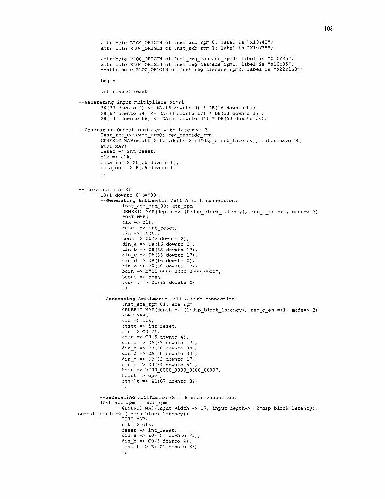
108
attribute RLOC_ORIGIN of lnst_acb_rpm_0: label is "X13Y43"; attribute RLOC_ORIGIN of Inst_acb_rpm_l: label is "X10Y75";
attribute RLOC_ORIGIN of Inst_reg_cascade_rpmO: label is "X10Y85"; attribute RLOC_ORIGIN of Inst_reg_cascade_rpml: label is "X10Y95"; —attribute RLOCJDRIGIN of Inst_reg_cascade_rpm2: label is "X22Y150";
begin
int_reset<=reset;
—Generating input multipliers Xi*Yi Z0(33 downto 0) <= DA(16 downto 0) * DB(16 downto 0); Z0(67 downto 34) <= DA(33 downto 17) * DB(33 downto 17); Z0(101 downto 68) <= DA(50 downto 34) * DB(50 downto 34);
—Generating Output register with latency: 3 Inst_reg_cascade_rpmO: reg_cascade_rpm GENERIC MAP(width=> 17 ,depth=> (3*dsp_block_latency), interleave=>0) PORT MAP( reset => int_reset, elk => elk, data_in => Z0(16 downto 0), data_out => R(16 downto 0) ) ;
—iteration for Zl C0(1 downto 0)<="00"; —Generating Arithmetic Cell A with connection:
lnst_aca_rpm_00: aca_rpm GENERIC MAP(depth => (O*dsp_block_latency), reg_c_en =>1, mode=> 3) PORT MAP( elk => elk, reset => int_reset, cin => C0(0), cout => CO(3 downto 2), din_a => DA(16 downto 0), din_b => DB(33 downto 17), din_c => DA(33 downto 17), din_d => DB(16 downto 0), din_e => Z0(50 downto 17), bcin => b"00_0000_0000_0000_0000", bcout => open, result => Zl(33 downto 0) );
—Generating Arithmetic Cell A with connection: Inst_aca_rpm_01: aca_rpm GENERIC MAP(depth => (l*dsp_block_latency), reg_c_en =>1, mode=> 3) PORT MAP( elk => elk, reset => int_reset, cin => CO (2), cout => CO(5 downto 4), din_a => DA(33 downto 17), din_b => DB(50 downto 34), din_c => DA(50 downto 34), din_d => DB(33 downto 17), din_e => Z0(84 downto 51), bcin => b"00_0000_0000_0000_0000", bcout => open, result => Zl(67 downto 34) ) ;
—Generating Arithmetic Cell B with connection: lnst_acb_rpm_0: acb_rpm
GENERIC MAP(input_width => 17, input_depth=> (2*dsp_block_latency), output_depth => (l*dsp_block_latency))
PORT MAP( elk => elk, reset => int_reset, din_a => Z0(101 downto 85), din_b => CO(5 downto 4), result => R(101 downto 85) ) ;

109
—Generating Output register with latency: 2 Inst_reg_cascade_rpml: reg_cascade_rpm
GENERIC MAP(width=> 17 ,depth=> (2*dsp_block_latency), interleave=>0) PORT MAP( reset => int_reset, elk => elk, data_in => Zl(16 downto 0), data_out => R(33 downto 17) );
—iteration for Z2 Cl(l downto 0)<="00"; —Generating Arithmetic Cell A with connection:
Inst_aca_rpm_ll: aca_rpm GENERIC MAP(depth => (2*dsp_block_latency), reg_c_en =>0, mode=> 1) PORT MAP( elk => elk, reset => int_reset, cin => CI (0), cout => CI(3 downto 2), din_a => DA(16 downto 0), din_b => DB(50 downto 34), din_c => DA(50 downto 34), din_d => DB(16 downto 0), din_e => Zl(50 downto 17), bcin => b"00_0000_0000_0000_0000", bcout => open, result => Z2(33 downto 0) );
—Generating Arithmetic Cell B with connection: Inst_acb_rpm_l: acb_rpm
GENERIC MAP(input_width=>17, input_depth => (0*dsp_block_latency), output_depth => (0*dsp_block_latency))
PORT MAP( elk => elk, reset => int_reset, din_a => Zl(67 downto 51), din_b => CI(3 downto 2), result => R(84 downto 68) );
—Generating Output register with latency: 0 Inst_reg_cascade_rpm2: reg_cascade_rpm
GENERIC MAP(width=> 17 ,depth=> (0*dsp_block_latency), interleave=>0) PORT MAP( reset => int_reset, elk => elk, data_in => Z2(16 downto 0), data_out => R(50 downto 34) );
R(67 downto 51) <= Z2(33 downto 17);
—Done! —Statistics- Input multiplier: 3 —Statistics- DSP slice count: 9 Register count: 1768 —Statistics- ACA: 3 ACB: 2 CR: 2 —Statistics- Total external DSP block register: 18 —Statistics- Total ACB block register: 3 --Statistics- Total CR register: 5 end behavioral;

110
APPENDIX B, C++ SOURCE CODE

I l l
// Programmer: Jacques Laurent Athow // Objective: C++ source to implement proposed partition algorithm //' Project: Master thesis, Concordia. University, November 2008
#include "stdafx.h" #include <math.h> ttinclude <iostream> #include <string> using namespace std;
int _tmain(int argc, _TCHAR* argv[]) {
const int len=68; //const int N = 3; //number of levels const int m=17; //size of multiplier operands const int dsp_blk_k=4; char buff[100]; char x; int xO; int mode=0;
int N=(int)ceil((double)len/m)-1; int dsp_block_count=0; int register_count=0; int cella=0, cellb=0, cellc=0; int aca_reg=0; int cr_reg=2*N-l; int acb_reg=N; int au=0;
cout<<"—Number of levels is: "<<N<<endl;
cout<<"—Generating signal declaration\n"; for (int i=0; i<N+l; i++){
sprintf(buff, "\tsignal 2%i : std_logic_vector(%i downto 0);\n", i, (N-i+l)*m*2-l );
cout<<buff; } for (int i=0; i<N; i++){
sprintf(buff, "\tsignal C%i : std_logic_vector(%i downto 0);\n", i, 2*(N+l-i)-l);
cout<<buff; ) cout«endl;
//—iteration for Z0 first level output cout«"--Generating input multipliers Xi*Yi\n"; for (int i=0; i<N+l; i++){
sprintf(buff, "\tlnst_mult_dsp_%i: mult_dsp port map(dout=>Z0 (%i downto %i), din_a=>DA(%i downto %i), din_b=>DB(%i downto %i));\n",
//sprintf (buff, "\tZ0(%i downto %i) <:= DA(%i downto %i) * DB(%i downto »i);\n",
i, 2*m*(i+l)-l, 2*m*i, m*(i+l)-l, m*i, m*(i+l)-l, m*i);
cout<<buff; } cout«"\n--Generat ing Output reg i s te r with latency: " « 2 * N - l « e n d l ; cout<<"\tlnst_reg_cascade0: reg_cascade_rprn\n"; sprintf(buff, "\tGENERIC MAP(width=> 17 ,depth=> (%i*dsp_block_latency),
interleave=>%i)\n", 2*N-1, 0); cout<<buff;
cout«"\tPORT MAP(\n"; c o u t « " \ t r e s e t => in t_rese t , \n"; c o u t « " \ t c l k => c lk , \n" ; cou t«" \ t da t a_ in => Z0(16 downto 0) , \n" ; cou t«" \ tda ta_out => R(16 downto 0)\n"; c o u t « " \ t ) ; \n \n" ;
for (int i=0; i<N; i++)( cout«"\n\n—iteration for Z"«i+l«"\n"; sprintf(buff, "\tC%i(l downto 0)<=\"00\";\n", i); cout<<buff; int j ; for (j=i; j< N; j++)(
aca_reg+=(4*(i+j));

112
if (i==N-l) mode=l;
else{ mode=3; aca_reg++;
}
cout<<"\t—Generating Arithmetic Cell A with connection:\n";
if (i==0){ if (mode==3)
au=34*(3+4*(i+j)+(2*4*(i+j))); else
au=34*(l+4*(i+j)+(2*4*(i+j)));
sprintf(buff, "\t—Area utilization: %i\n", au) ; cout<<buff; sprintf(buff, "\tlnst_aca_rpm_%i%i: aca_rpm\n", i, j); cout<<buff; sprintf(buff, "\t\tGENERIC MAP(depth =>
(%i*dsp_block_latency), reg_c_en =>%s, mode=> %i)\n", i+j, "1", mode); aca_reg+=2;}
else{ if (mode==3)
au=34*(3+(2*4*(i+j) ) ) ; else
au=34*(l+(2*4*(i+j))) ;
sprintf(buff, "\t—Area utilization: %i\n", au); cout<<buff; sprintf(buff, "\tlnst_aca_rpm_%i%i: aca_rpm\n", i, j) ; cout<<buff; sprintf(buff, "\t\tGENERIC MAP(depth =>
(%i*dsp_block_latency), reg_c_en =>%s, mode=> %i)\n", i+j, "0", mode);} cout«buf f ;
cout«"\t\tPORT MAP(\n"; cout«"\t\tclk => clk,\n"; cout«"\t\treset => int_reset, \n";
sprintf (buff, "\t\tcin => C%i(%i),\n", i, (j-i)*2); cout«buff ; sprintf(buff, "\t\tcout => C%i(%i downto %i),\n", i, (j+2-i)*2-
1, (j + l-i)*2);
m*(j-i));
m*(j+l));
m*(j+l));
m*(j-i));
cout«buff ;
sprintf(buff, "\t\tdin_a => DA(%i downto %i),\n", m*(j-i+l)-l,
cout<<buff; sprintf(buff, "\t\tdin_b => DB(%i downto %i),\n", m*(j+2)-l,
cout<<buff; sprintf(buff, "\t\tdin_c => DA(%i downto %i),\n", m*(j+2)-l,
cout<<buff; sprintf(buff, "\t\tdin_d => DB(%i downto %i),\n", m*(j-i+1)-1,
cout<<buff; sprintf(buff, "\t\tdin_e => Z%i(%i downto %i),\n", i, 2*m*(j-
i+l)-l+m, m*(2*(j-i)+l)); cout«buf f ;
c o u t « " \ t \ t b c i n => b\"00_0000_0000_0000_0000\", \n"; cout<<"\t\tbcout => open,\n";
i+l)-l, 2*m*(j-i)), sprintf(buff, "\t\tresult => Z%i(%i downto %i)\n", i+1, 2*m*(j-
cout«buf f ;
cout«"\t\t) ;\n"; cout«endl;
cella++; ) //implement the output registers and arithmetic cell B

113
cout«"\t—Generating Arithmetic Cell B with connection: \n";
if (i==0) xO=N;
else x0=0;
acb_reg+=N-i-l;
sprintf (buff, "\t—Area utilization: %i\n", 17* (xO+N-i-1)*4); cout<<buff;
sprintf(buff, "\tlnst_acb_dsp48_rpm_%i: acb_dsp4 8_rpm\n", i); cout<<buff; sprintf(buff, "\t\tGENERIC MAP(input_width=>17, input_depth =>
(%i*dsp_block_latency), output_depth => (%i*dsp_block_latency))\n", xO, N-i-1); cout<<buff;
sprintf(buff, "\t\tPORT MAP(\n"); cout<<buff; sprintf(buff, "\t\tclk => clk,\n"); cout<<buff; sprintf(buff, "\t\treset => int_reset,\n"); cout<<buff; sprintf(buff, "\t\tdin_a => Z%i(%i downto %i),\n", i, m*(2*(j-i)+2)-1,
m*(2*(j-i)+l) ); cout<<buff; sprintf(buff, "\t\tdin_b => C%i(%i downto %i),\n", i, (j+l-i)*2-l, (j-
i)*2);
i+D) ;
l)«endl;
cout«buff; sprintf(buff, "\t\tresult => R(%i downto %i)\n", (2*N+2-i)*m-l, m*(2*N-
cout<<buff; sprintf(buff, "\t\t);\n"); cout<<buff;
cout<<"\n\t—Generating Output register with latency: "«2*(N-i-
sprintf(buff, "\t—Area utilization: %i\n", 34*(N-i-1)*4); cout<<buff; sprintf(buff, "\tlnst_reg_cascade_rpm%i: reg_cascade_rpm\n", i+1); cout<<buff; sprintf(buff, "\t\tGENERIC MAP(width=> 17 , depth=>
(%i*dsp_block_latency), interleave=>%i)\n", 2* (N-i-1), 0); cout<<buff;
cr_reg+=2*(N-i-1);
cout<<"\t\tPORT MAP(\n"; cout<<"\t\treset => int_reset,\n"; cout<<"\t\tclk => clk,\n"; sprintf(buff, "\t\tdata_in => Z%i(16 downto 0),\n", i+1); cout<<buff; sprintf (buff, "\t\tdata_out => R(%i downto %i)\n", m*(i+2)-l, m*(i+l)), cout<<buff; cout<<"\t\t);\n\n";
if (i==N-l)( sprintf (buff, "\tR(%i downto %i) <= Z%i(33 downto 17),An",
m*(i+3)-l, m*(i+2), i+1); cout«buf f «endl ;
} cellb++; cellc++;
) cout<<"—Done!"<<endl; cout<<"—Statistics- Input multiplier: "«N+l«endl; cout<<"--Statistics- ACA register count : "«aca_reg«" , ACB register count :
"<<acb_reg<<" , CR register count : "<<cr_reg; cout<<"—Statistics- DSP slice count: " « (cella*2) + (N+l) « " Register count:
" « (aca_reg+acb_reg+cr_reg) *dsp_blk_k*m<<endl; cout<<"—Statistics- ACA: "«cella<<" ACB: "«cellb«" CR: "<<cellc<<endl; cout<<"—Statistics- Total external DSP block register: "<<aca_reg«endl; cout<<"—Statistics- Total ACB block register: "«acb_reg<<endl; cout<<"—Statistics- Total CR register: "«cr_reg«endl;

114
cin>>x; return 0;
#include "stdafx.h" #include <math.h> •include <iostream> •include <string>
•include "graph.h" •include "HPLAN.h" •include "quicksort.h" •include "fpga_resource.h"
using namespace std;
float k=0.5;
i n t _ t m a i n ( i n t a r g c , _TCHAR* a r g v [ ] ) (
int seed=0; int threshold=ll;
String fpga_type="XC4V140FX"; List* curr_list_ptr=openDesign() ; List bounding_boxl_list, bounding_box2_list; Elem generic_elem, generic_eleml; Hplan hplan(seed);
buildResource(fpga_type);
//build bounding box lists while(curr_list_ptr->size())(
generic_elem=new Elem(curr_list_ptr->getElem()); if (generic_elem.type()==ACA)
bounding_box_listl.addElem(generic_elem); if (generic_elem.type()==ACB)
bounding_box_list2.addElem(generic_elem); }
curr_list_ptr=openDesign() ; quicksort(curr_list_ptr) ; do{
generic_elem=new(generic_elemcurr_list_ptr->removeElem()); cout<<"now placing: "<<generic_elem.getInfo()<<endl; if (generic_elem.type()==ACA SS
(generic_elem.getPredecessor()).type()==ACB)( cout<<"ACA is largest block..."<<endl; cout<<"Placing it and its predecessor"<<endl realPlacer(generic_elem, hplan, bounding_box_listl,
bounding_box_list2),
bounding_box_list2) ,
) else)
bounding_box_list2); }
cout«"Predecessor is: "; generic_eleml=new element(generic_elem.getSuccessor()); cout«generic_eleml. getlnf o () <<endl ; realPlacer(generic_eleml, hplan, bounding_box_listl,
//modified to avoid segmentation of interconnect if (threshold>curr_list_ptr->size())
break;
realPlacer(generic_elem, hplan, bounding_box_listl.
}while(curr_list_ptr->size() ) ;
hplan.validate();
cout<<"Done with placing!\r\n";
cin>>x;

115
return 0; )
void realPlacer(Elem working_element, Hplan & hplan_working, List working_listl, List working_list2){
int size_x=working_element.getXSize(); int size_y=working_element.getYSize();
working_element.adjustSlack(size_x*k, size_y*k);
hplan_working.getFreeResource(working_listl, 0); hplan_working.placeElement(working_element);
hplan_working.getFreeResource(working_listl, 1) ; hplan_working.placeElement(working_element);