Embed Size (px)
Citation preview

Enhancing efficiency of organic light-emitting diodes using a
carbon nanotube-doped hole injection layer
Shui-Hsiang Su*, Wang-Ta Chiang, Chung-Ting Kuo, Yu-Che Liu, Meiso Yokoyama
Department of Electronic Engineering, I-Shou University
1, Section 1, Hsueh-Cheng RD, Ta-Hsu Hsiang, Kaohsiung County, Taiwan
*E-mail: [email protected]
Abstract Nanocomposite layers consisting of multi-walled carbon nanotubes
(MWCNTs)-doped poly(3,4,-ethylene dioxythiphene):polystyrene sulfonic
acid (PEDOT:PSS) were employed as a hole injection layer (HIL) in organic
light-emitting diodes (OLEDs). The structure of OLED is glass/indium-tin
oxide (ITO)/MWCNTs-doped PEDOT:PSS/PEDOT:PSS/
tris(8-hydroxyquinolinato)aluminium (Alq3)/LiF/Al. The luminous efficiency
of the OLED is as high as 2.1 cd/A, which is 70% higher than that of a
conventional device without a MWCNTs-doped HIL. A device with a
‘‘hole-only” structure, ITO/MWCNTs-doped PEDOT:PSS/Al, was constructed to
elucidate the mechanism of carrier injection and transporting. The MWCNTs-doped
PEDOT:PSS layer exhibits a low carrier transporting ability.
Keywords: Multi-wall carbon nanotubes; PEDOT:PSS; organic light-emitting
diodes

Introduction
Efficient organic light-emitting devices (OLEDs), that based on small
molecular organic materials or polymers, have attracted extensive research
interest because of their potential application to full-color flat panel displays.
Significant progress has recently been made in improving the characteristics
of device’s structure for emissive display applications [1,2]. Fluorescent
emission in OLEDs is associated with the radiative recombination of singlet
excitons. One of them is an imbalance of electron and hole mobilities [3,4],
which results in a shift of the recombination zone toward an electrode,
lowering the device efficiency due to exciton quenching by the metal electrode.
Polymer/carbon nanotube (CNT) nanocomposite has been regarded as a
solution to low electron mobility [5-8], and the polymer/CNT junctions act as
exciton quenching centers, improving charge transport and quenching
photoluminescence [9-12]. More balanced charge injection is associated with
higher external quantum efficiency of the OLED. A key discovery of recent
years is that doping improves emission efficiency and intensity. The
predominant electronic interaction in the nanocomposite s is known to be
polymer-to-CNT photoinduced charge (electron) transfer [13-15], while
photoinduced energy (exciton) transfer has been suggested to occur in the
polymer/CNT bilayer [16]. However, while various potential applications of
CNTs have been suggested, few practical uses have been realized. The main
difficulties concern the poor purity and process ability of MWCNTs that
contain powder.
In this investigation, the prepared MWCNTs were purified and then doped
as a very small fraction of up to 2.5 wt% into extensively used PEDOT:PSS.
Double-layer and hole-only devices were fabricated, and the device
characteristics were studied to examine the role of MWCNTs in OLEDs.
Experimental Details
The MWCNTs in this investigation were synthesized using chemical
vapor deposition (CVD) and purified following a standard procedure. 100mg
of MWCNTs powder was added to 50ml of a mixture of sulfuric acid and nitric
acid in a 3:1 ratio, and the mixture was stirred for 15min on a hot plate at 100°
C. The suspension was then diluted to 200ml. Finally, the MWCNTs were
collected by membrane filtration (0.45 μm pore size), and washed with
sufficient deionized water to remove residual acids. The PEDOT:PSS solution
was filtered through a 0.45 μm polyvinyl difluoride (PVDF) syringe filter.
Purified MWCNTs was doped into PEDOT:PSS solution with concentrations

of 0, 0.7, 1.5 and 2.5 wt%. The mingle solution in an ultrasonic bath for
approximately 24 hr. OLEDs were fabricated as follows. ITO-coated glass
substrates (with a sheet resistance of 7Ω/) were cleaned by ultrasonic in a
detergent solution and deionized water. A HIL of MWCNTs-doped
PEDOT:PSS nanocomposite was spin-coated on the optically transparent ITO
glass substrates at 3000 rpm, which were then backed for 1 hr at 120°C in a
vacuum oven. The other layers (organic layer and Al cathode) of the devices
were fabricated by conventional thermal evaporation in a high vacuum
chamber at a base pressure of 5×10⁻⁶ Torr without breaking the vacuum. The
deposition rate of the organic layer was 0.05 nm/s and that of the Al metal
cathode was 0.5 nm/s. Figure 1 shows the structure and energy-level diagrams
of the OLEDs. The device consists of a 120 nm-thick anode layer of ITO, a 60
nm HIL of MWCNTs-doped PEDOT:PSS, a 60 nm emissive layer and
electron-transporting layer (ETL) of Alq3, a 0.7 nm electron injection layer of
lithium fluoride (LiF) and a 150 nm cathode layer of aluminum (Al). The
transmission electron micrographs of MWCNTs-doped PEDOT:PSS
nanocomposite s film were obtained using an FEI Tecnai transmission electron
microscope (TEM) with a point-to-point resolution of 0.14 nm. The surfaces
of the films were analyzed using atomic force microscopy (AFM). The

current-voltage characteristics were measured using a Keithley 2400 source
meter, and the luminance of OLEDs was measured using a PR-650
spectrometer. All the measurements were made in the dark at room
temperature.

Results and discussion
Untreated pristine MWCNTs were doped into the PEDOT:PSS to act as an
HIL in an OLED. However, poor optoelectronic characteristics of OLED have
been observed- even an absence of light emission at a very high driving
current. Several investigations have suggested that acid treatment can cut
MWCNTs and shorten them, while reducing the diameter of MWCNTs [17-20].
It can also remove amorphous carbon and contaminating metals. Figure 2
shows TEM images of MWCNTs after acid treatment. As shown in Fig. 2(a),
acid treatment removed contaminating metallic catalyst from the top of the
graphite tube wall. Figure 2(b) demonstrates that treatment with 1:3 HNO3:H2SO4
acidic solution for 48 hr produces a sharp graphite tube wall, indicating that the
MWCNTs had been cut off and thereby shortened. Figure 3 plots the J-V
characteristics of OLEDs with PEDOT:PSS doped with various concentrations of
MWCNTs. As the fraction of MWCNTs increases, the current density declines
and the turn-on voltage increases. The purification of the prepared MWCNTs
is critical to making the MWCNTs an effective material in the fabrication of
OLEDs. Impurities such as amorphous and metallic catalytes in solution
remarkably degrade the physical and chromatic characteristics of the device -
especially at the interface and inside the bulk.

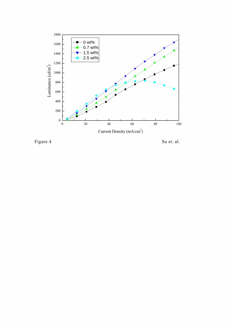
Figure 4 plots the luminance-current density characteristics of the OLEDs.
OLEDs with MWCNTs-doped PEDOT:PSS HIL exhibit higher luminance. The
OLEDs with 1.5 wt% MWCNTs-doped PEDOT:PSS HIL had a luminance of
1650 cd/m2 at a current density of 100 mA/cm2. Figure 5 presents the
calculated luminous efficiency. The overall trend in which associated property
in the observed luminance of the undoped devices equals that of the doped
ones. The luminous efficiency of MWCNTs-doped devices increases with the
concentration of MWCNTs. One plausible cause is the retard of
hole-transporting and polymer-nanotube interactions, which rigidify the
polymer chains. The device with 1.5 wt% doping has higher luminous efficiency.
However, the luminous efficiency of the 2.5 wt% MWCNTs-doped device falls
sharply as the current density rises above 30 mA/cm2. Doping PEDOT:PSS with
excess MWCNTs may destroy the polymer chain, reducing luminous efficiency at
high current density.
The variation of the surface roughness caused by MWCNTs-doping in
PEDOT:PSS might affect the performance of OLEDs. An OLED employing an
MWCNTs-doped PEDOT:PSS HIL covered by PEDOT:PSS had been prepared.
Luminous efficiency can be increased to 2.1 cd/A at a current density of 60 mA/m2. It
is 70% higher than that of the conventional device without a MWCNTs-doped

PEDOT:PSS HIL. The surface roughness of MWCNTs-doped PEDOT:PSS on
ITO was investigated by the tapping mode AFM and shown in Figs. 6 (a) and
(b). The root-mean-square (RMS) surface roughness of MWCNTs-doped
PEDOT:PSS was approximately 10.86 nm, whereas bestrew smooth layer the
RMS of the PEDOT:PSS was approximately 1.74 nm. Obviously, the smooth
layer can provide the better surface contact between HIL and EML interface.
It was reported that the HIL with smaller roughness led to the enhanced device
performance.
It is well known that the driving voltage depends on the carrier injection
and transporting, while current efficiency depends not only on carrier
injection, but also on the balance of electrons and holes. To verify the
hole-transporting ability of the MWCNTs-doped PEDOT:PSS HIL, the devices with
‘‘hole-only” structures were fabricated by sandwiching the MWCNTs-doped
PEDOT:PSS or pristine PEDOT:PSS films between two electrodes (ITO and
Al) and their electrical properties were examined. The device structure was
ITO/MWCNTs-doped PEDOT:PSS/Al. The concentrations of MWCNTs were 0 and
2.5 wt%. Figure 7 plots the current density–voltage curves of the hole-only devices.
At the driving voltage of 5 V, 2.5 wt% MWCNTs-doped PEDOT:PSS device
produced a current density of 318 mA, which was much lower than 645 mA for the

undoped device. On the other hand, under the current density of 200 mA/cm2, the
voltage drop of 2.5 wt% MWCNTs-doped PEDOT:PSS device is 3.3 V, which is
much larger than 1.7 V for the undoped device. This indicates that the
MWCNTs-doped PEDOT:PSS layer exhibits a low carrier transporting ability.
Conclusion
This study investigated the feasibility of using MWCNTs-doped
PEDOT:PSS as an HIL in OLEDs. The structure of OLED was
glass/ITO/MWCNTs-doped PEDOT:PSS/PEDOT:PSS/Alq3/LiF/Al. Research
into a nanocomposite of PEDOT:PSS and MWCNTs has clearly demonstrated
that the MWCNTs can be easily purified, processed and used as an effective
material in OLEDs. The luminous efficiency of the OLED is 2.1 cd/A, which
is 70% higher than that of a conventional device without a MWCNTs-doped
PEDOT:PSS HIL. A smooth layer covering on the MWCNTs-doped
PEDOT:PSS improves the surface roughness and further enhances the
luminous efficiency. The hole-only device reveals that the MWCNTs-doped
PEDOT:PSS layer exhibits a low carrier transporting ability. MWCNTs can be a
candidate in such a form in organic solar cells or other organic optoelectronic
devices.
Acknowledgements

The authors would like to thank the National Science Council of the
Republic of China, Taiwan, for financially supporting this research under
Contract No. NSC 96-2221-E-214-015 and NSC 96-2221-E-214-016. The
authors would also like to thank the MANALAB at ISU, Taiwan.

References
[1] S. H. Su, M. Yokoyama, J. F. Li, and K. S. Hwang, J. Electrochemical Soc.,
153 (2006).
[2] G. T. Chen, S. H. Su, C. C. Hou, and M. Yokoyama, J. Electrochemical
Soc., 154 (2007).
[3] H. C. F. Martens, J. N. Huiberts, and P. W. Blom, Appl. Phys. Lett. 77, 1852
(2000).
[4] B. K. Crone, I. H. Campbell, P. S. Davids, and D. L. Smith, Appl. Phys. Lett.
73, 3162 (1998).
[5] X.-Z. Bo, C. Y. Lee, M. S. Strano, M. Goldfinger, C. Nuckolls, and G. B.
Blanchet, Appl. Phys. Lett. 86, 182102 (2005).
[6] E. Mulazzi, R. Perego, H. Aarab, L. Mihut, S. Lefrant, E. Faulques, and J.
Wery, Phys. Rev. B 70, 155206 (2004).
[7] S. A. Curran, P. M. Ajayan, W. J. Blau, D. L. Carroll, J. N. Coleman, A.B.
Dalton, A. P. Davey, A. Drury, B. McCarthy, S. Maier, and A. Strevens, Adv.
Mater. (Weinheim, Ger.) 10, 1091 (1998).
[8] D. S. Ginger and N. C. Greenham, Phys. Rev. B 59, 10622 (1999).
[9] J. Wéry, H. Aarab, S. Lefrant, E. Faulques, E. Mulazzi, and R. Perego, Phys.
Rev. B 67, 115202 (2003).
[10] E. Kymakis, I. Alexandou, and G. A. J. Amaratunga, Synth. Met. 127, 59
(2002).
[11] H. Ago, K. Petritsch, M. S. P. Shaffer, A. H. Windle, and R. H. Friend,Adv.
Mater. (Weinheim, Ger.)11, 1281 (1999).
[12] J. N. Coleman, S. Curran, A. B. Dalton, A. P. Davey, B. McCarthy, W. Blau,
and R. C. Barklie, Phys. Rev. B 58, R7492 (1998).

[13] C. Yang, M. Wohlgenannt, Z. V. Vardeny, W. J. Blau, A. B. Dalton, R.
Baughman, and A. A. Zakhidov, Physica B 338, 366 (2003).
[14] E. Kymakis and G. A. J. Amaratunga, Appl. Phys. Lett. 80, 112 (2002).
[15] B. McCarthy, A. B. Dalton, J. N. Coleman, H. J. Byrne, P. Bernier, and W. J.
Blau, Chem. Phys. Lett. 350, 27 (2001).
[16] H. Ago, M. S. P. Shaffer, D. S. Ginger, A. H. Windle, and R. H. Friend, Phys.
Rev. B 61, 2286 (2000).
[17] Gavin A. Forrest and Andrew J. Alexander J. Phys. Chem. C, 111,
10792-10798 (2007) [18] Wiltshire, J. G.; Khlobystov, A. N.; Li, L. J.; Lyapin, S. G.; Briggs, G.
A. D.; Nicholas, R. J. Chem. Phys. Lett. 386, 239 (2004)
[19] Nagasawa, S.; Yudasaka, M.; Hirahara, K.; Ichihashi, T.; Iijima, S.
Chem. Phys. Lett. 328, 374. (2000)
[20] Zhang, M.; Yudasaka, M.; Iijima, S. J. Phys. Chem. B 108,149 (2004)

Figure captions
Fig. 1 (a) Structure and (b) energy-level diagram of OLEDs.
Fig. 2 TEM images of MWCNTs treated with acidic H2SO4/HNO3
mixture.
Fig. 3 J-V characteristics of OLEDs with various weight percentages of
MWCNTs doped in PEDOT:PSS films.
Fig. 4 Luminance-current density characteristics of OLEDs with various weight
percentages of MWCNTs doped in PEDOT:PSS films.
Fig. 5 Luminous efficiency-current density characteristics of OLEDs with
various weight percentages of MWCNTs doped in PEDOT:PSS films.
Fig. 6 AFM images of (a) ITO/MWCNTs-doped PEDOT:PSS and (b) ITO/MWCNTs-doped PEDOT:PSS/PEDOT:PSS.
Fig. 7 Current-voltage characteristics of hole-only devices. The inset is structure of the hole-only device.

ITO4.7ev
PEDOT
:PSS
Alq3
5.2ev
5.7ev
3.5evLiF/Al
3.1ev
MWNT
h+
e-
ITO Glass MWCNTs-doped PEDOT:PSS
Alq3
LiF/Al
Figure 1 Su et. al.

(a) (b)
Figure 2 Su et. al.

0 2 4 6 80
100
200
300
400
500
Cur
rent
Den
sity
(mA
/cm
2 )
Voltage (V)
0wt% 0.7wt% 1.5wt% 2.5wt%
Figure 3 Su et. al.
0 20 40 60 80 10
200
400
600
800
1000
1200
1400
1600
1800
00
Lum
inan
ce (c
d/m
2 )
Current Density (mA/cm2)
0 wt% 0.7 wt% 1.5 wt% 2.5 wt%
Figure 4 Su et. al.

0 20 40 60 80
0.0
0.4
0.8
1.2
1.6
2.0
2.4
100
Lum
inou
s Effi
cien
cy (c
d/A
)
Current Density (mA/cm2)
0wt% 0.7wt% 1.5wt% 2.5wt% 1.5wt%+smooth layer
Figure 5 Su et. al.

(a) (b)
igure 6 Su et. al. F

0 2 4 6 80
200
400
600
800
1000
1200
10
Cur
rent
Den
sity
(mA
/cm
2 )
Voltage (V)
0 wt% 2.5 wt%
Figure 7 Su et. al.