Embed Size (px)
Citation preview
Thin Solid Films 517 (2009) 2012–2015
Contents lists available at ScienceDirect
Thin Solid Films
j ourna l homepage: www.e lsev ie r.com/ locate / ts f
Effects of welding head on the carbon nanotube field emission inultrasonic nanowelding
Bo Zhao ⁎, Changxin Chen, Boluo Yadian, Ping Liu, Zijiong Li, Dong Xu, Yafei Zhang ⁎National Key Laboratory of Nano/Micro Fabrication Technology, Key Laboratory for Thin Film and Microfabrication of the Ministry of Education, Research Institute of Micro/NanometerScience & Technology, Shanghai Jiao Tong University, Shanghai 200240, PR China
⁎ Corresponding authors. Tel./fax: +86 21 6293 2017.E-mail addresses: [email protected] (B. Zhao), y
0040-6090/$ – see front matter © 2008 Elsevier B.V. Adoi:10.1016/j.tsf.2008.09.092
a b s t r a c t
a r t i c l e i n f oArticle history:
Ultrasonic nanowelding tec Received 14 November 2007Received in revised form 4 July 2008Accepted 24 September 2008Available online 7 October 2008Keywords:Carbon nanotubeElectrical properties and measurementsField emissionScanning electron microscopyUltrasonic nanowelding
hnique was used to improve the field emission properties of carbon nanotube(CNT) cathodes. Two kinds of welding heads were used and the effects of the head on the emission propertieswere studied. The results show that cathodes welded by Al2O3 flat head demonstrate excellent field emissionproperties with high emission current density and good current stability. The improved field emissionperformance is attributed to the reliable and low resistance contact between CNTs and metal substrates.Cathodes welded by steel matrix head show a lower turn-on electric field due to the protruding CNTs at theedge of the welded pits.
© 2008 Elsevier B.V. All rights reserved.
1. Introduction
Building reliable interconnections between one-dimensional nano-materials and the external electrical circuits is oneof themost importantissues in nanoelectronics. Many physical and chemical processes havebeen explored to address this need. It had been shown that metal-carbon nanotube (CNT) contact resistance could be reduced by exposingthe contact area to focused electron beam [1] or ion beam [2]. However,thesemethods are not easy to realize in real situation due to the limitedaccess to a focused beam. High-temperature annealing method wasdemonstrated to be able to improve the metal–CNT contacts [3,4].However, high temperature used in this method will produce manyunexpected side effects on the devices. Joule-heating-induced nanospotwelding of CNTs [5,6] involves complicated transmission electronmicroscope operation and low yield, which significantly limits theirapplications. In addition, chemical modification of the electrodes wasused to enhance the adsorption between CNT and electrodes [7,8];however, a stronger bonding instead of a weak chemical adsorption ismandatory for constructing reliable nanodevices.
Ultrasonic nanowelding is a promising technique to create reliablecontact between one-dimensional nanomaterials and electrodes[9,10]. The contacts formed by this simple method have demonstratedlow contact resistance, good long-term stability and mechanicalstrength. CNTs are promising candidates for cold cathodefield emitters[11,12]. However, the realization of CNTfield emission devices has been
[email protected] (Y. Zhang).
ll rights reserved.
limited due to the absence of a stable emitter fabricationprocess.Manyapproaches have been tried as possible fabrication techniques such asdirect growth [13], screen-printing [14], spraying [15] and electro-phoretic deposition [16]. Most of them have some disadvantages, suchas high complexity and high cost of the technological process for thedirect growth, or the producing of reactionless conducting chemicalsfor printing technologies. Spraying and electrophoretic deposition aresimple methods and can be used to fabricate a large area of coldcathode. However, poor adhesion of CNTs to the substrate is adrawback. In this paper, Ultrasonic nanowelding was used to obtainstable CNT field emitting cathodes and the effects of the welding headon the carbon nanotube field emission were studied.
2. Experimental details
The CNT cathodes were fabricated by electrophoretic depositionmethod. Themultiwall carbon nanotubes produced by chemical vapordeposition have a specific diameter 10–30 nm and the purity is higherthan 95%. The pristine CNTs were first treated at temperature of1500 °C under vacuum of 10–4 Pa. The high-temperature vacuumprocess efficiently removed residual metal catalysts and enhanced thegraphitization of the CNTs [17]. Then, the CNTs were treated withmixed acid (HNO3:H2SO4=3:1) at 90 °C for 70 min. 7 mg of the treatedCNTs were dispersed in 700 ml of acetone solution that contained3.5 mg of dissolved Mg(NO3)2. The CNT electrophoresis suspensionwas ultrasonically dispersed for about 3 h. The Ti-coated glass wafer asa cathode and a stainless steel plate as an anode were immersed intothe CNT electrophoresis suspension at room temperature. The twoelectrodes were kept at a constant gap of 2 cm for 10 min under the
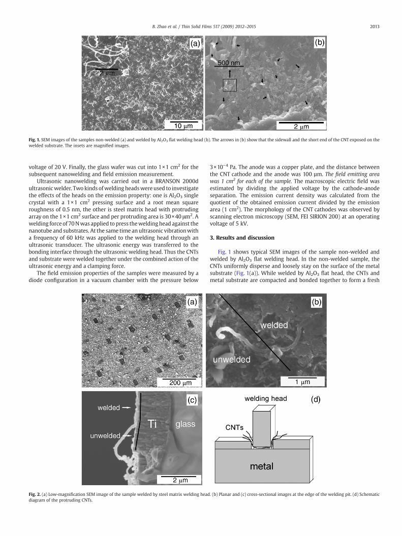
Fig. 1. SEM images of the samples non-welded (a) and welded by Al2O3 flat welding head (b). The arrows in (b) show that the sidewall and the short end of the CNT exposed on thewelded substrate. The insets are magnified images.
2013B. Zhao et al. / Thin Solid Films 517 (2009) 2012–2015
voltage of 20 V. Finally, the glass wafer was cut into 1×1 cm2 for thesubsequent nanowelding and field emission measurement.
Ultrasonic nanowelding was carried out in a BRANSON 2000dultrasonicwelder. Twokinds ofweldingheadswereused to investigatethe effects of the heads on the emission property: one is Al2O3 singlecrystal with a 1×1 cm2 pressing surface and a root mean squareroughness of 0.5 nm, the other is steel matrix head with protrudingarray on the 1×1 cm2 surface and per protruding area is 30×40 μm2. Awelding force of 70Nwas applied to press theweldinghead against thenanotube and substrates. At the same time an ultrasonic vibrationwitha frequency of 60 kHz was applied to the welding head through anultrasonic transducer. The ultrasonic energy was transferred to thebonding interface through the ultrasonic welding head. Thus the CNTsand substrate werewelded together under the combined action of theultrasonic energy and a clamping force.
The field emission properties of the samples were measured by adiode configuration in a vacuum chamber with the pressure below
Fig. 2. (a) Low-magnification SEM image of the sample welded by steel matrix welding headdiagram of the protruding CNTs.
3×10⁻⁴ Pa. The anode was a copper plate, and the distance betweenthe CNT cathode and the anode was 100 µm. The field emitting areawas 1 cm2 for each of the sample. The macroscopic electric field wasestimated by dividing the applied voltage by the cathode-anodeseparation. The emission current density was calculated from thequotient of the obtained emission current divided by the emissionarea (1 cm2). The morphology of the CNT cathodes was observed byscanning electron microscopy (SEM, FEI SIRION 200) at an operatingvoltage of 5 kV.
3. Results and discussion
Fig. 1 shows typical SEM images of the sample non-welded andwelded by Al2O3 flat welding head. In the non-welded sample, theCNTs uniformly disperse and loosely stay on the surface of the metalsubstrate (Fig. 1(a)). While welded by Al2O3 flat head, the CNTs andmetal substrate are compacted and bonded together to form a fresh
. (b) Planar and (c) cross-sectional images at the edge of the welding pit. (d) Schematic
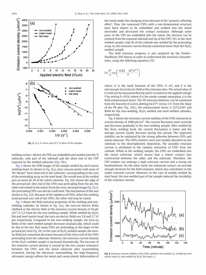
Fig. 3. (a) J–E curves and (b) F–N plots of the samples.
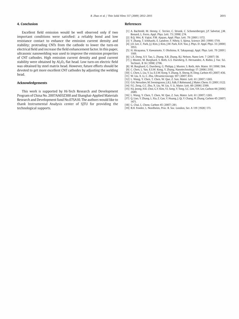
Fig. 4. Emission current stability of the CNTs cathodes non-welded (a), welded by steelmatrix head (b) and welded by Al2O3 flat head (c).
2014 B. Zhao et al. / Thin Solid Films 517 (2009) 2012–2015
welding surface. Almost all CNTs are embedded andwelded into the Tisubstrate, only part of the sidewall and the short end of the CNTexposed on the welded substrate (Fig. 1(b)).
Fig. 2 shows the SEM images of the sample welded by steel matrixwelding head. As shown in Fig. 2(a), clear concave prints with areas of30×40 μm2 were observed in the substrate, corresponding to the areaof the protruding array on the steel head. The overall area of the weldedpart accounts for 4% of the whole substrate. Fig. 2(b) shows the edge ofthe pressed pit. One end of the CNTs was protruding from the pit, theother end rooted in themetal. From the cross-sectional image Fig. 2(c)),the protruding CNTs can also be confirmed. Themechanism of thiswasshown in Fig. 2(d). Because of the rigidness of CNTs, when theweldinghead pressed one end of the CNTs, the other end may be raised.
Fig. 3 shows the field emission properties of the welding and non-welding cathodes. As shown in Fig. 3(a), the turn-on electric fields(defined as the electric field at the emission current density of 10 μA/cm2) is 5.2 V/μm for the non-welding sample. While welded by Al2O3
flat and steel matrix head, the turn-on electric fields are 3.8 and 2.7 V/µm respectively. Compared to the non-welding sample, the turn-onfields of the steel welded sample decreases dramatically, which couldbe due to the fact that many CNTs are protruding at the edges of thepressed pit (seen Fig. 2b). In the case of Al2O3welded sample, the turn-on field just somewhat decreases because of the short end of the CNTsprotruding from the substrate. However, the emission current densityof the Al2O3 welded sample is increased dramatically. The increase ofthe emission current density is caused by the low contact resistancebetween the CNTs and the metal substrate after nanoweldingtreatment. During the ultrasonic nanowelding, the high-frequencyultrasonic energy softens the metal and causes plastic deformation of
the metal under the clamping stress because of the ‘acoustic softeningeffect’. Thus, the nanosized CNTs with a one-dimensional structurehave been shown to be embedded and welded into the metalelectrodes and decreased the contact resistance. Although someparts of the CNT are embedded into the metal, the electron can beemitted from the exposed sidewall and tip of the CNT [18]. In the steelwelded sample, only 4% of the cathode was welded by the protrudingarray, so, the emission current density somewhat lower than the Al2O3
welded sample.The field emission property is also analyzed by the Fowler–
Nordheim (FN) theory in order to understand the emission character-istics, using the following equation [19]
I~E2
/exp
−6:83� 107Φ3=2
E
!
where Φ is the work function of the CNTs (5 eV) and E is themicroscopic local electric field at the emission sites. The actual value ofE could not bemeasured directly and it is related to the applied voltageV by setting E=βV/d, where d is the anode-sample separation, β is thefield enhancement factor. The FN emission behavior can be examinedfrom the linearity of curves plotting ln(I/V2) versus 1/V. From the slopeof the FN plot (Fig. 3(b)), the enhancement factor is 2273,5347 and8944 for the non-welding, Al2O3 welded and steel welded cathodes,respectively.
Fig. 4 shows the emission current stability of the CNTs measured atcurrent density of 1000 μA/cm2. The current fluctuates more severelyand decreases gradually in the non-welding sample. After welded byflat Al2O3 welding head, the current fluctuation is lower and theaverage current hardly decrease during this period. The improvedstability can be explained by the strong adhesion between CNTs andmetal substrate. The CNTs emitters were just weakly adsorbed on thesubstrate in the electrophoretic deposition. The unstable emissioncurrent is attributed to the random extraction of CNTs from thecathode. While in the welding sample, the CNTs are embedded intothe metal substrate, which means that a robust contact wasconstructed between the tubes and the substrate. Therefore, theCNT emitter can undergo a high emission current and a strong ionbombardment. On the other hand, the enhanced contact can provideenough electrons for the field emission, which also contributes to thestable emission current. However, in the case of sample welded bysteel head, the non-welded part of the sample induced the instabilityof the emission current.
2015B. Zhao et al. / Thin Solid Films 517 (2009) 2012–2015
4. Conclusion
Excellent field emission would be well observed only if twoimportant conditions were satisfied: a reliably bond and lowresistance contact to enhance the emission current density andstability; protruding CNTs from the cathode to lower the turn-onelectrical field and increase the field enhancement factor. In this paper,ultrasonic nanowelding was used to improve the emission propertiesof CNT cathodes. High emission current density and good currentstability were obtained by Al2O3 flat head. Low turn-on electric fieldwas obtained by steel matrix head. However, future efforts should bedevoted to get more excellent CNT cathodes by adjusting the weldinghead.
Acknowledgements
This work is supported by Hi-Tech Research and DevelopmentProgram of China No. 2007AA03Z300 and Shanghai-AppliedMaterialsResearch and Development fund No.07SA10. The authors would like tothank Instrumental Analysis center of SJTU for providing thetechnological supports.
References
[1] A. Bachtold, M. Henny, C. Terrier, C. Strunk, C. Schonenberger, J.P. Salvetat, J.M.Bonard, L. Forro, Appl. Phys. Lett. 73 (1998) 274.
[2] B.Q. Wei, R. Vajtai, P.M. Ajayan, Appl. Phys. Lett. 79 (2001) 1172.[3] Y. Zhang, T. Ichihashi, E. Landree, F. Nihey, S. Iijima, Science 285 (1999) 1719.[4] J.O. Lee, C. Park, J.J. Kim, J. Kim, J.W. Park, K.H. Yoo, J. Phys. D: Appl. Phys. 33 (2000)
1953.[5] H. Hirayama, Y. Kawamoto, Y. Ohshima, K. Takayanagi, Appl. Phys. Lett. 79 (2001)
1169.[6] L.X. Dong, X.Y. Tao, L. Zhang, X.B. Zhang, B.J. Nelson, Nano Lett. 7 (2007) 58.[7] J. Muster, M. Burghard, S. Roth, G.S. Duesberg, E. Hernandez, A. Rubio, J. Vac. Sci.
Technol., B 16 (1998) 2796.[8] M. Burghard, G. Duesberg, G. Philipp, J. Muster, S. Roth, Adv. Mater. 10 (1998) 584.[9] C. Chen, L. Yan, E.S.W. Kong, Y. Zhang, Nanotechnology 17 (2006) 2192.[10] C. Chen, L. Liu, Y. Lu, E.S.W. Kong, Y. Zhang, X. Sheng, H. Ding, Carbon 45 (2007) 436.[11] W. Liu, X. Li, C. Zhu, Ultramicroscopy 107 (2007) 833.[12] L. Wang, Y. Chen, T. Chen, W. Que, Z. Sun, Mater. Lett. 61 (2007) 1265.[13] O.A.Nerushev,M.Sveningsson, L.K.L. Falk, F. Rohmund, J.Mater. Chem.11 (2001)1122.[14] F.G. Zeng, C.C. Zhu, X. Liu, W. Liu, Y. Li, Mater. Lett. 60 (2006) 2399.[15] H.J. Jeong, H.K. Choi, G.Y. Kim, Y.I. Song, Y. Tong, S.C. Lim, Y.H. Lee, Carbon 44 (2006)
2689.[16] L. Wang, Y. Chen, T. Chen, W. Que, Z. Sun, Mater. Lett. 61 (2007) 1265.[17] Q. Liao, Y. Zhang, L. Xia, Z. Gao, Y. Huang, J. Qi, Y. Chang, H. Zhang, Carbon 45 (2007)
1471.[18] G. Chai, L. Chow, Carbon 45 (2007) 281.[19] R.H. Fowler, L. Nordheim, Proc. R. Soc. London, Ser. A 119 (1928) 173.