Embed Size (px)
Citation preview
Diamond Films and Technology
Vol. 5, No.6 1995
MYU Tokyo
DFI' 084
Effects of Surface Treatments on SecondaryElectron Emission from CVD Diamond Films
G. T. MearinF, I. L. Krainsky, J. A. Dayton, Jr., Christian Zorman*,
Yaxin Wang* and A. Lamouri*
NASA Lewis Research Center, Cleveland, Ohio 44135
*General Vacuum, lnc., P. O. Box 605204, Cleveland, Ohio 44105, U.S.A.
(Received 13 October 1995; accepted 8 January 1996)
Key words: diamond, CVD, secondat 3, electron emission
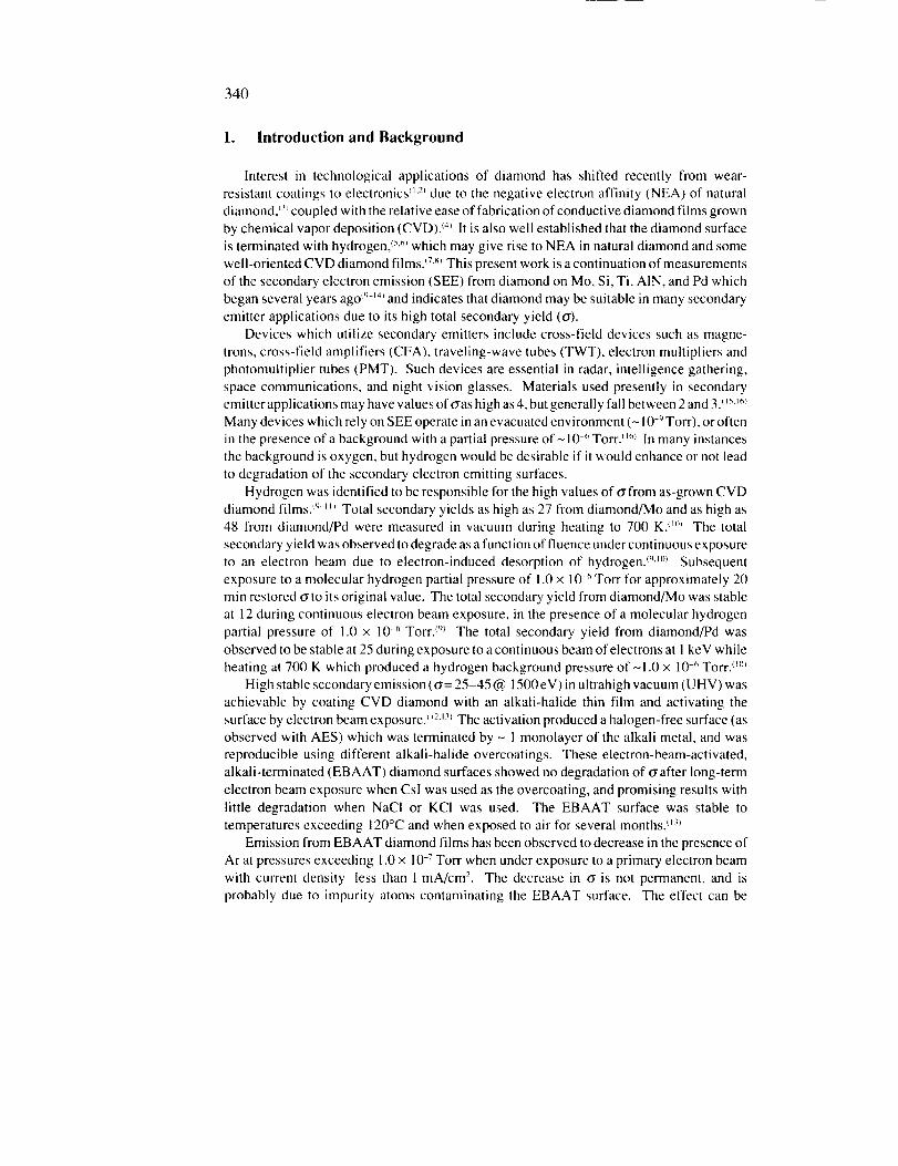
Secondary electron emission (SEE) properties of polycrystalline diamond films grown
by chemical vapor deposition (CVD) were measured. The total secondary yield (_r) from
as-grown samples was observed to be as high as 20 at room temperature and 48 while heating
at 700 K in vacuum. Electron-beam-activated, alkali-terminated diamond films have shown
stable values of o'as high as 60 when coated with Csl and similarly high values when coated
with other alkali halides. Diamond coated with BaF, had a stable o of 6, but no enhancement
of the SEE properties was observed with coatings of Ti or Au. Hydrogen was identified to
give rise to this effect in as-grown films. However, electron beam exposure led to a reduction
in o-to values as low as 2. Exposure to a molecular hydrogen environment restored crto its
original value after degradation, and enabled stable secondary emission during electron
beam exposure. Atomic hydrogen and hydrogen plasma treatments were performed on
diamond/Mo samples in an attempt to increase the near-surface hydrogen concentration
which might lead to increased stability in the secondary emission. Raman scattering
analysis, scanning electron microscopy, and Auger electron spectroscopy (AES) confirmed
that hydrogen plasma and atomic hydrogen treatments improved the quality of the CVD
diamond significantly. Elastic recoil detection (ERD) showed that heating as-grown
diamond targets to 700 K, which was correlated with an increase in o', removed contaminants
from the surface but did not drive hydrogen from the diamond bulk. ERD showed that the
hydrogen plasma treatment produced an increase in the hydrogen concentration in the near-
surface region which did not decrease while heating in vacuum at 700 K, but no improvement
in the SEE properties was observed.
_Present address: General Vacuum, Inc., P.O. Box 605204, Cleveland, Ohio 44105
339
https://ntrs.nasa.gov/search.jsp?R=19970027992 2018-11-10T20:52:58+00:00Z
340
1. Introduction and Background
Interest in technological applications of diamond has shifted recently from wear-
resistant coatings to electronics _L2_due to the negative electron affinity (NEA) of natural
diamond, _3_coupled with the relative ease of fabrication of conductive diamond fihns grown
by chemical vapor deposition (CVD)/4_ It is also well established that the diamond surface
is terminated with hydrogen, '_._ which may give rise to NEA in natural diamond and some
well-oriented CVD diamond films. _7,x_This present work is a continuation of measurementsof the secondary electron emission (SEE) from diamond on Mo, Si, Ti, AIN, and Pd which
began several years ago _'_-t4_and indicates that diamond may be suitable in many secondary
emitter applications due to its high total secondary yield (0").
Devices which utilize secondary emitters include cross-field devices such as magne-
trons, cross-field amplifiers (CFA), traveling-wave tubes (TWT), electron multipliers andphotomultiplier tubes (PMT). Such devices are essential in radar, intelligence gathering,
space communications, and night vision glasses. Materials used presently in secondary
emitter applications may have values of o'as high as 4, but generally fall between 2 and 3._t_,_6_
Many devices which rely on SEE operate in an evacuated environment (- 10-9 Torr), or often
in the presence of a background with a partial pressure of-10 6Torr._6_ In many instances
the background is oxygen, but hydrogen would be desirable if it would enhance or not lead
to degradation of the secondary electron emitting surfaces.
Hydrogen was identified to be responsible for the high values of o"from as-grown CVD
diamond films/_ t_, Total secondary yields as high as 27 from diamond/Mo and as high as48 from diamond/Pd were measured in vacuum during heating to 700 K. _"' The total
secondary yield was observed to degrade as a function of fluence under continuous exposure
to an electron beam due to electron-induced desorption of hydrogen. _,"'_ Subsequent
exposure to a molecular hydrogen partial pressure of 1.0 × 10 .6 Torr for approximately 20
min restored oto its original value. The total secondary yield from diamond/Mo was stable
at 12 during continuous electron beam exposure, in the presence of a molecular hydrogen
partial pressure of 1.0 × 10 -6 Torr/'_ The total secondary yield from diamond/Pd was
observed to be stable at 25 during exposure to a continuous beam of electrons at I keV while
heating at 700 K which produced a hydrogen background pressure of-l.0 × 10 -6 Torr/_'
High stable secondary emission (o-= 25-45 @ 1500 eV) in ultrahigh vacuum (UHV) wasachievable by coating CVD diamond with an alkali-halide thin film and activating the
surface by electron beam exposure. __2._3,The activation produced a halogen-free surface (as
observed with AES) which was terminated by - 1 monolayer of the alkali metal, and was
reproducible using different alkali-halide overcoatings. These electron-beam-activated,
alkali-terminated (EBAAT) diamond surfaces showed no degradation of o'after long-term
electron beam exposure when Csl was used as the overcoating, and promising results with
little degradation when NaCI or KCI was used. The EBAAT surface was stable to
temperatures exceeding 120°C and when exposed to air for several months. __3_
Emission from EBAAT diamond films has been observed to decrease in the presence of
Ar at pressures exceeding 1.0 × 10 -7 Tort when under exposure to a primary electron beam
with current density less than 1 mA/cm 2. The decrease in t7 is not permanent, and is
probably due to impurity atoms contaminating the EBAAT surface. The effect can be
341
reversedbyeitheranincreaseinprimarycurrentdensityoradecreaseinpressure.However,forthisreasontheEBAATdiamondis notnecessarilyasdesirableasthehydrogen-terminateddiamondforspecificapplications.Also,NEAobservationsfromdiamondcoatedwiththinfilms(submonotayerandmonolayercoverages)ofTiandCo_7._7_suggestthattheseorothermaterialsmayproducehighstable<3-andallowoperationathighertemperatures.Theseconsiderationswerethemotivationforthiswork.
2. Experimental Procedure
SEE measurements were conducted in a UHV chamber with a base pressure of 1.0 × 10 "'
Ton'. The experimental setup has been described previously. '9_ The samples tested were p-
type diamond films on Mo and Si substrates, ranging from I/Jm to 20_m in thickness, grown
by hot filament (HF) and microwave plasma (MP) CVD. Total secondary yield vs. primary
beam energy (Ev,,,,,,,_) was measured for all samples, where E v........_ ranged from 100 eV to 3keV in 50 eV increments. To investigate the effects of beam exposure on or,each sample was
exposed to the electron beam for up to 72 h at current densities ranging from 50 MA/cm'- to
10.0 mA/cm 2. The beam diameter ranged from 0.12 to 0.25 ram. The current density was
held constant during each experiment and the data were normalized by comparing the
fluence dependence of each sample. In all cases the data were collected every 5 s while the
primary beam energy was held constant in the range 1.0 to 1.5 keV.
Each as-deposited sample was tested prior to any hydrogen treatment, after which each
sample was subjected to a molecular hydrogen treatment, an atomic hydrogen treatment, a
hydrogen plasma treatment, or a combination of these. The SEE measurements were
repeated on the treated samples.
Scanning electron microscopy (SEM), Raman scattering analysis, and Auger electron
spectroscopy (AES) were used to determine the effects of the hydrogen treatments on the
diamond samples. Rutherford backscattering spectroscopy (RBS) was used to investigate
the purity of the diamond bulk, and elastic recoil detection (ERD) was used to characterize
bulk and near-surface hydrogen concentrations in the diamond samples, as-grown and afterhydrogen treatments. ERD was also used to detect changes in the hydrogen concentrations
during heating at 700 K, which might be responsible for the increase in cr observed
previouslyJ_ t_>AES was used to investigate changes in the shape of the carbon peak from
CVD diamond/Si due to ionic bombardment, indicating graphitization of the diamondsurface.
BaF, coatings, 30 nm thick, were resistively evaporated onto diamond targets in a
diffusion-pumped high-vacuum system with a base pressure of 2 x 1()-_ Torr. Thin coatings
of Ti and Au, ranging from < 1 monolayer to 30 nm in thickness, were vacuum-deposited
from a resistively heated source onto diamond targets in a turbopumped preparation chamberattached to the main UHV test chamber and separated with a gate valve. SEE properties of
these samples were measured as described above. Thin CsI coatings were deposited onto
representative diamond samples from the depositions used for Ti and Au coatings, and the
targets were used as control samples to ensure that diamond films from different depositions
had similar SEE properties.
342
3. Experimental Results
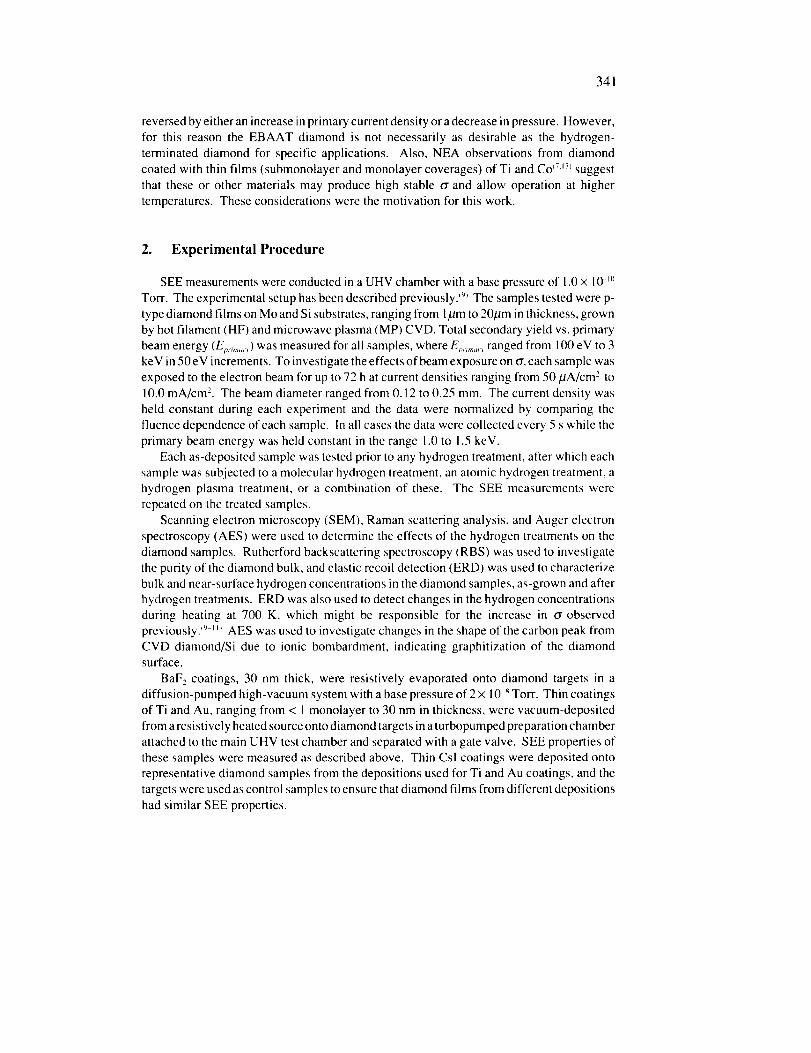
SEE measurements from as-grown samples have been discussed previously _" _' and
some results will be included here for comparison. Figures 1 and 2 show crvs. Ep, i,,,, , andcrvs. fluence data from representative CVD diamond targets, respectively. No differences
in the SEE results have been observed to arise from the different deposition techniques
(HFCVD and MPCVD). _wax from as-grown samples nominally occurred between 1000
and 1500 eV, and ranged from 10 to 20 as seen in Fig. 1. As-grown CVD diamond/Pd had
O'_faxof- 20 at 1400 eV, and O'MAXof 48 at 3 keV while being heated in vacuum at 700 K. _m_
EBAAT diamond/Mo bad _.ax of 50-60 at 3 keV at room temperature. _3. _8_
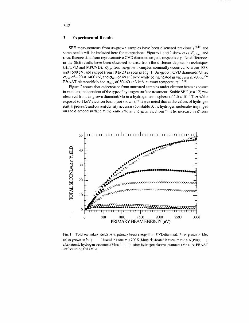
Figure 2 shows that crdecreased from untreated samples under electron beam exposure
in vacuum, independent of the type of hydrogen surface treatment. Stable SEE (or= 12) was
observed from as-grown diamond/Mo in a hydrogen atmosphere of 1.0 x 10 6 Torr while
exposed to 1 keV electron beam (not shown). _9_It was noted that at the values of hydrogen
partial pressure and current density necessary for stable or,the hydrogen molecules impingedon the diamond surface at the same rate as energetic electronsJ _ The increase in cr from
!40 ' '" '
_ °°o_AO;A AAA Z
-- AOO?;A.,_A _
-- OV AA --30-- 00_ -AAAA'O" 0500_0500Q050550000500_$_ --
_ OAA_ 000000 O0 --'_'_O_
: ,..*,.'oo°° Z20 -- _o ° ---
-- . AlP'___O . vvxXXXXXXXXXXXXXXXXXXXXXXXXXXXXXXXXXXXX;_
- _z_liu xxX xxX^^/" X
E z__,_x x _v_wvvvvvvvvwvvv,,v_10 [- _ ..._ vvvwv,7 ........... -I
......0 i_[_l
0 500 1000 1500 2000 2500 3000
PRIMARY BEAM ENERGY (eV)
Fig. 1. Total secondary yield (o3 vs. primary beam energy from CVD diamond: (V)as-grown on Mo;
(×)as-grown on Pd; ( ) heated in vacuum at 700 K (Mo); ( _I,)heated in vacuum at 700 K (Pd);( )
after atomic hydrogen treatment (Mo); ( £ ) after hydrogen plasma treatment (Mo); (A) EBAATsurface using Csl (Mo).
343
3O
25-
20-
15-
10-
5-
IlllJlt_lllllJLJlJlllllJlJllllll'''''''l'_'JJllll
A
, .., # .= # .= ¢ _ #
," "%.
\
"" "•- "_ "_ " '0 - ....
_---k- --_ _---k _---_- --_--- i---_k----,,_- i--=_--
0.00 0.40 1.60
zB
7_.__
-_.._
0.80 1.20
FLUENCE (C/cm 2)
2.00
Fig. 2. Tolalsecondaryyield(o')vs.fluencefromCVDdiamondatlkeV:(g)as-grownonMo;( )
heated in vacuum at 700 K (Mo); ( • ) heated in vacuum at 700 K (Pd): ( ) after atomic hydrogen
treatmenl(Mo);( £ )afterhydrogenplasmatreatment(Mo).
diamond/Mo while heating is seen from all diamond targets and is probably due to initial
desorption of surface contaminants. This effect was not observed in the other curves because
data collections began after initial beam exposure.Stable 6 > 25 from diamond/Pd was also observed when the sample was heated in
vacuum at 700 K (cf. Fig. 2) while the target was exposed to 1keV electron beam. _m, At thistemperature the Pd substrate provided a hydrogen background pressure of 1.0 × I0 _'Tort,
which was sufficient to replenish the surface hydrogen desorbed by the electron beam. After
sufficient heating, hydrogen stored in the Pd substrate was depleted and o" decreased with
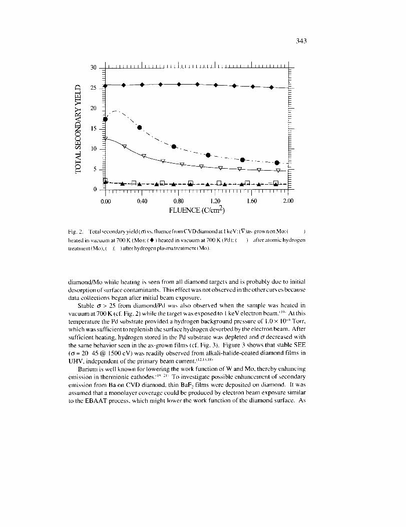
the same behavior seen in the as-grown films (cf. Fig. 3). Figure 3 shows that stable SEE
(o-= 20-45 @ 1500 eV) was readily observed from alkali-halide-coated diamond films in
UHV, independent of the primary beam current. _'2'3_
Barium is well known for lowering the work function of W and Mo, thereby enhancing
emission in themfionic cathodes? _'; 2t, To investigate possible enhancement of secondary
emission from Ba on CVD diamond, thin BaF 2 films were deposited on diamond. It was
assumed that a monolayer coverage could be produced by electron beam exposure similar
to the EBAAT process, which might lower the work function of the diamond surface. As
344
50
40-
i20
S
-...
Z
Z
\\ Z
\
''"l'"'l''"l""l''"l'"'l'"'l'"'l'"'l'"'0 15 30 45 60 75 90 105 120 135 150
FUmNCE(C/cm2)
Fig. 3. Total secondary yield (o) vs. fluence at 1.5 keV: (solid line) EBAAT diamond/Si using CsI;(short dashed line) diamond/Pd during heating in vacuum at 700 K; (long dashed line) diamond/Sicoated with 30 nm BaF 2.
is seen in Fig. 3, _yvs. fluence from BaF2-coated diamond showed a behavior similar to that
of EBAAT samples. However, the maximum value of cr never exceeded 6 at 1.5 keV in
samples of diamond/Si coated with 30 nm BaF> Csl-coated diamond films from the same
diamond-coated Si wafers used with BaF2 had values of or> 30 under the same operating
parameters.
The fluence dependence of crfrom diamond in vacuum during exposure to an electron
beam, shown in Fig. 2, has been observed in all as-grown CVD diamond targets tested,
independent of the current density or the substrate material. It was observed previously that
energetic primary electrons induced hydrogen desorption from the diamond surface, whichresulted in lower cr (cf. Fig. 2).
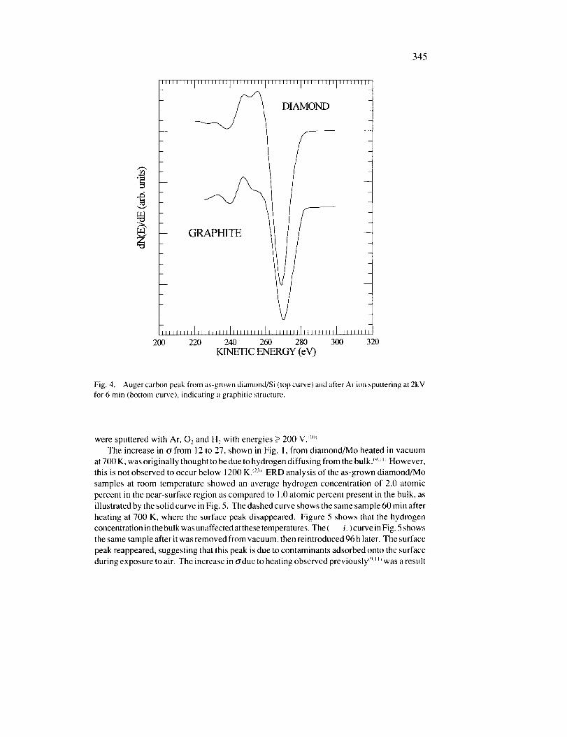
The Auger carbon peaks from an as-grown diamond surface, before and after Ar ion
sputtering at 2kV, are shown in Fig. 4. Before sputtering the signature Auger diamond peak
was observed, a2_ After sputtering for 6 rain the diamond structure was destroyed, as
indicated by the shape of the Auger carbon peak. Ion bombardment using oxygen at 2kV,
and hydrogen to as low as 200 V, produced the same change in the carbon peak from CVDdiamond targets. This graphitization of the diamond surface due to ion bombardment is
responsible for the reduction in crto that of ordinary carbon observed when diamond targets
345
DIAMOND
GRAPHITE
\I_]llLllll]ll]][][[ltl]]]j]][]]l[lllll]l]]llll]l]nllltll
200 220 240 260 280 300
KINETIC ENERGY (eV)
II
_20
Fig. 4. Auger carbon peak from as-grown diamond/Si (top curve) and after Ar ion sputtering at 2kVfor 6 rain (bottom curve), indicating a graphitic structure.
were sputtered with Ar, O 2and H_ with energies _>200 VY °_
The increase in _from 12 to 27, shown in Fig. 1, from diamond/Mo heated in vacuumat 700 K, was originally thought to be due to hydrogen diffusing from the bulk. _,_ However,
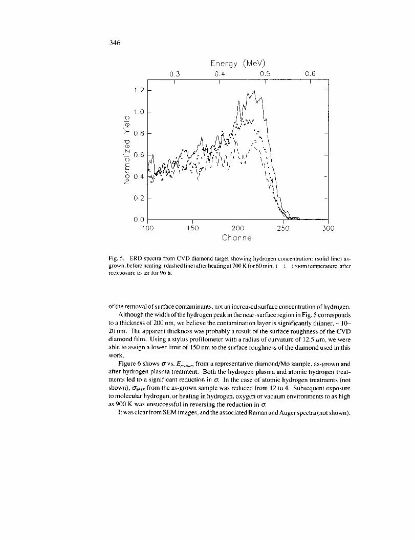
this is not observed to occur below 1200 K. _2_ ERD analysis of the as-grown diamond/Mo
samples at room temperature showed an average hydrogen concentration of 2.0 atomic
percent in the near-surface region as compared to 1.0 atomic percent present in the bulk, as
illustrated by the solid curve in Fig. 5. The dashed curve shows the same sample 60 rain after
heating at 700 K, where the surface peak disappeared. Figure 5 shows that the hydrogen
concentration in the bulk was unaffected at these temperatures. The ( f_) curve in Fig. 5 shows
the same sample after it was removed from vacuum, then reintroduced 96 h later. The surface
peak reappeared, suggesting that this peak is due to contaminants adsorbed onto the surface
during exposure to air. The increase in o-due to heating observed previously _,__ was a result
346
1.2
1.0q:D
>7 0.8
"_0,6
k-
o 0.4Z
0.2
Energy (MeV)
0..3 0.4 0.5 0.6I I I I
-^ /'1" f. _ , I I ,,,/
0.0 n I i100 150 200 250 500
Channel
Fig. 5. ERD spectra from CVD diamond target showing hydrogen concentration: (solid line) as-
grown, before heating; (dashed line) after heating at 700 K for 60 min; ( £. ) room temperature, after
reexposure to air for 96 h.
of the removal of surface contaminants, not an increased surface concentration of hydrogen.
Although the width of the hydrogen peak in the near-surface region in Fig. 5 corresponds
to a thickness of 200 nm, we believe the contamination layer is significantly thinner, - 10-
20 nm. The apparent thickness was probably a result of the surface roughness of the CVDdiamond film. Using a stylus profilometer with a radius of curvature of 12.5/Jm, we were
able to assign a lower limit of 150 nm to the surface roughness of the diamond used in thiswork.
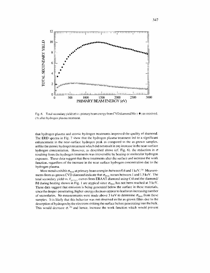
Figure 6 shows o"vs. Ep,.,m_,_from a representative diamond/Mo sample, as-grown andafter hydrogen plasma treatment. Both the hydrogen plasma and atomic hydrogen treat-
ments led to a significant reduction in o'. In the case of atomic hydrogen treatments (not
shown), O'MAx from the as-grown sample was reduced from 12 to 4. Subsequent exposure
to molecular hydrogen, or heating in hydrogen, oxygen or vacuum environments to as high
as 900 K was unsuccessful in reversing the reduction in o'.
It was clear from SEM images, and the associated Raman and Auger spectra (not shown),
347
12
10
4
2
00
OO Ov TvOOOO_OOOi.- _
4,
41,
41,
,e'
_O
Z
IllllIBl[lllLItll,llllllllllltJltlllllllllllllJl[llllll_lT-500 1000 1500 2000 2500 3000
PRIMARY BEAM ENERGY (eV)
Fig. 6. Total secondary yield (o3 vs. primary beam energy from CVD diamond/Mo: ( 0 ) as-received:
(A) after hydrogen plasma treatment.
that hydrogen plasma and atomic hydrogen treatments improved the quality of diamond.
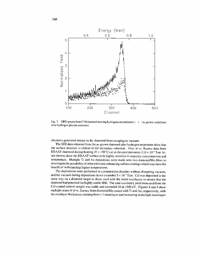
The ERD spectra in Fig. 7 show that the hydrogen plasma treatment led to a significantenhancement in the near-surface hydrogen peak as compared to the as-grown samples.
unlike the atomic hydrogen treatment which did not result in any increase in the near-surface
hydrogen concentration. However, as described above (cf. Fig. 6), the reduction in crresulting from the hydrogen treatments was irreversible by heating or molecular hydrogen
exposure. These data suggest that these treatments alter the surface and increase the work
function, regardless of the increase in the near surface hydrogen concentration due to the
hydrogen plasma.
Most metals exhibit o'uax at primary beam energies between 0.6 and I keV. _24_Measure-
ments from as-grown CVD diamond indicate that o'._,_xoccurs between I and 1.5 keV. The
total secondary yield vs. E;,,,,,,,,, curves from EBAAT diamond using Csl and the diamond/
Pd during heating shown in Fig. 1 are atypical since O'MAXhas not been reached at 3 keV.
These data suggest that emission is being generated below the surface in these materials,
since the deeper-penetrating, higher-energy electrons appear to lead to an increasing numberof secondaries. No measurements were made above 3 keV to determine crMa_,from these
samples. It is likely that this behavior was not observed in the as-grown films due to thedesorption of hydrogen by the electrons striking the surface before penetrating into the bulk.
This would decrease o',c]°' and hence, increase the work function which would prevent
348
2:3
(b
>-
_D0ON
O
EL.
OZ
Energy (MeV)O.4 0.6
I I
0.8 1.0I
_-" i* i i i0 i t i100 200 ,.300 400 500
Channel
Fig. 7. ERDspectrafromCVDdamondshowinghydrogenconcentration:( £ )as-grown;(solidline)
after hydrogen plasma treatment.
electrons generated deeper in the diamond from escaping to vacuum.
The SEE data obtained from the as-grown diamond after hydrogen treatments show thatthe surface structure is critical to the secondary emission. Also, cr vs. fluence data from
EBAAT diamond during heating (T > 150°C) or at elevated pressures ( 1.0 × 10⁻⁶ Torr Ar,
not shown) show the EBAAT surface to be highly sensitive to impurity concentrations and
temperature. Multiple Ti and Au depositions were made onto two diamond/Mo films to
investigate the possibility of other emission-enhancing surface coatings which may have thebenefit of withstanding higher temperatures.
The depositions were performed in a preparation chamber without disrupting vacuum,
and the vacuum during depositions never exceeded 5 × 10 -7 Tort. CsI was deposited in the
same way on a diamond target as those used with the metal overlayers to ensure that the
diamond had potential for highly stable SEE. The total secondary yield measured from the
Csl-coated control sample was stable and exceeded 30 at 1500 eV. Figures 8 and 9 show
multiple scans of crvs. fluence from diamond/Mo coated with Ti and Au, respectively, with
the overlayer thicknesses starting from < 1 monolayer and increasing in multiple monolayer

349
20
!,6
8
"'"'"'1'"'"'"1"'"'"'1'""'"'1'"'"'"1'"'"'"
UNCOATED
/ / Ti on DIAMONIYMoPRIMARY CURRENT = 0.42 uAPRIMARY ENERGY = 1070 eV
\.',_ _.4am
Fig. 8. T_ta__ec_ndaryyie_d(_.)vs._uencefr_mCVDdiam_nd/M_aftersuc_essivedep_siti_ns_fTi.
10
_6_4
0.4 am Au on DIAMO_
PRIMARY CURRENT = 0.42 uAI PRIMARY ENERGY = 1074eV
1.0nm i BIAS =-215 V
/ 1.4nm I
_ 4.2nm
• 6.2 am 8.2 nm 30.0 am
Fig. 9. Total secondary yield (m vs. fluence from CVD diamond/Mo after successive depositions of Au.
350
increments. The overlayer materials were chosen based on emission-enhancing effectsreported in the literature. Ti/diamond has been reported as a NEA material, _7_and thin Au
films have been reported to stabilize field emission from CVD diamond films. _2_.2_With
each successive deposition CYMAx was reduced, until the SEE behavior became that of theoverlayer material.
The apparent temporary recovery in the data from diamond coated with 0.4- and 1.0-nm-
thick Au films is probably due to mobile gold atoms under electron beam exposure. As the
surface was exposed and locally heated, Au atoms might gain sufficient energy to "hop" out,revealing a previously unexposed diamond surface. Thereafter the data follow the normal
behavior for hydrogen-terminated diamond. This behavior was observed at every pointtested on the diamond coated with 0.4- and 1.0-nm-thick Au. It was not observed after theAu thickness exceeded 1.0 nm.
4. Conclusions
High SEE has been observed from CVD diamond films grown on various substrates. In
as-grown films the effect is due to surface hydrogen which is unstable under exposure to an
electron beam. Alkali-halide coatings on the diamond films lead to highly stable emissionin UHV after the surface is activated by electron beam exposure. No differences in SEE
properties have been observed between samples grown by HFCVD or MPCVD. The SEE
properties appear to have little or no dependence on the substrate material, except in the caseof Pd substrate whcre heating induces a continuous flow of hydrogen from the Pd onto the
diamond surface, which stabilizes o'. Thin BaF2 coatings provided some enhancement in thestability of abut crMax was considerably lower than those for EBAAT surfaces or even as-grown films.
ERD showed that heating untreated samples at 700 K cleaned the surface, which led to
an increase in o'. The bulk hydrogen concentration was observed to remain unchanged at thistemperature.
Hydrogen plasma and atomic hydrogen treatments led to a significant, irreversible
reduction of o'from CVD diamond/Mo targets. Raman scattering Analysis, SEM, and AESshowed that the diamond surface was improved significantly by the treatments. ERD
showed that hydrogen plasma treatment led to a significant increase in the near-surface
hydrogen concentration. However, or,which is highly surface-sensitive, decreased after the
hydrogen treatments. This implies that SEE is dependent on surface hydrogen and is not
affected by the near-surface hydrogen concentration. The _ vs. Ep,,,,,,,y data from EBAAT
diamond coated with CsI show higher emission at higher primary energies, indicating thatelectrons generated deeper within the bulk drift to the surface and are emitted into the
vacuum. However, the data from as-grown films indicate that the surface propertiesultimately determine the SEE properties from CVD diamond.
Although Ti on diamond has been observed to be a NEA material when Ti is _< 1
monolayer thick, no SEE enhancing effect was observed when thin layers were depositedon diamond. The same results were observed with thin Au films.
351
Acknowledgments
The authors thank D. F. Anderson and his colleagues at Fermi Lab. for providing alkali
halides and "n" invaluable ideas. The authors would also like to thank Louis Maschak and
Ben Ebihara at NASA Lewis Research Center, and Robert Kusner and Robert Kunszt at
General Vacuum, Inc., for assisting with the experimental setup. ERD and RBS were
provided by R.W. Hoffman at the Ion Beam Analysis Facility of Case Western Reserve
University. Diamond targets were provided by R. Ramesham and M.F. Rose, Space Power
Institute, Auburn University, John Angus, Chemical Engineering Department, Case West-
em Reserve University, and General Vacuum, Inc. This work was supported by The
National Research Council and NASA Lewis Research Center.
References
1) M. Geis: Proc. of the IEEE 79 (5) ( 1991 ) 669.
2) M. Geis and J.C. Angus: Scientific American, Oct. (1992) 84.
3) F.J. Himpsel, J. A. Knapp+ J. A. Van Vechten and D. E. Eastman: Phys. Rev. B 20 (2) (19791624.
4) J.C. Angus, Y. Wang, and M. Sunkara: Annu. Rev. Mater. Sci. 21 (1991) 221.
5) B.B. Pate, M. H. Hecht, C. Binns, I. Lindau and W.E. Spicer: J. Vac. Sci. Technol. 21 (2) July/
Aug. (1982) 364.
6) B.J. Waclawski, D. T. Pierce, N. Swanson and R. J. Celotta: J. Vac. Sci. Technol. 21 (2) July/
Aug. (1982) 368.
7) J. van der Weide, Z. Zhang, P. K+ Baumann, M. G. Wensell, J. Bemholc and R. J. Nemanich:
Phys. Rev. B 50 (8) (1994) 5803.
8) I.L. Krainsky, V, M. Asnin, G. T. Mearini and J. A. Dayton, Jr., to be published in Phys. Rev.
Rapid Comm.
9) G.T. Mearini, I. L. Krainsky and J. A. Dayton, Jr.: Surf. and Int. Anal. 21 (2) (1994) 138.
10) G.T. Mearini, I. L. Krainsky, Y. X. Wang, J. A. Dayton, Jr., R. Ramesham and M.F. Rose: Thin
Solid Films 253 (1994) 151.
1 I ) T.L. Bekker, J. A. Dayton, Jr., A. S. Gihnour, Jr., I+L. Krainsky, M. F. Rose, R. Rameshan, D.
File and G. T. Mearini: IEEE IEDM Tech. Dig. (1992) 949.
12) G.T. Mearini, I. L. Krainsky, J. A.Dayton, Jr., Y. Wang, C. A. Zorman, J. C. Angus and R. W.
Hoffman: Appl. Phys. Lett. 65 (21) (1994) 2702.
13) G.T. Mearini, I. L. Krainsky, J. A. Dayton, Jr+, Y. Wang, C. A. Zorman, J. C. Angus, R. W.
Hoffman and D. F. Anderson: Appl. Phys. Lett. 66 (2) (1995) 242.
14) G.T. Mearini, I. L. Krainsky and J. A. Dayton, Jr.: Proc. of the Third Int. Conf. on Appl. of Diam.
Films and Rel. Mat., NIST Special Publication 885 (t995) 13.
15) E.A. Kurz: Amer. Lab., March (1979), and references therein.
16) A.S. Gilmour, Jr.: Microwave Tubes, Artech House, Norwood, MA (1986) 134-137.
17) P.K. Baumann and R. J+ Nemanich: Proc. of the Third Int. Conf. on Appl. of Diam. Films and
Rel. Mat., NIST Special Publication 885 (1995) 41.
18) i.L. Krainsky, V. M+ Asnin, G. T. Mearini and J. A. Dayton, Jr.: to be published in Appl. Phys.Lett.
19) A. Lamouri and 1. L. Krainsky: Surf. Sci. 278 (1992) 286.
20) A. Lamouri, I. L. Krainsky and W. Mueller: Surf. and Int. Anal. 21 (1994) 150.
352
21) A.Lamouri,W.MuellerandI.L.Krainsky:Phys.Rev.B50(1994)4764.22) P.G.Lurie and J. M. Wilson: Surf. Sci. 65 (1977) 476.
23) C.A. Fox, G. D. Kubiak, M. T. Schulberg and S. Hagstrom: Electrochemical Society Proc. of
the Third International Symposium on Diamond Materials (1993) 64.
24) I.M. Bronshtein and B. S. Fraiman: Secondary' Electron Emission, Nauka, Moscow (1969).
25) J.D. Shovlin and M. E. Kordesch: Appl. Phys. Lett. 65 (7) (1994) 863.
26) A. Lamouri, G. T. Mearini, Y. X. Wang and R. E. Kusner: Proc. of the Third Int. Conf. on Appl.
of Diam. Films and Rel. Mat., NIST Special Publication 885 (1995) 61.


![A Review of Heat Treatments on Improving the Quality and ......Laser Sintering (SLS), Selective Laser Melting (SLM), and Electron Beam Melting (EBM) (Figure1) [5]. However, if one](https://img.pdfslide.us/doc/110x75/611db5aff1fafb782f3cd5e0/a-review-of-heat-treatments-on-improving-the-quality-and-laser-sintering.jpg)