Embed Size (px)
Citation preview

Master Thesis
Effects of Interface and Surface Properties
on Silicon Nanowire Photovoltaics
A Dissertation Submitted to
the Department of Electronics and Applied Physics
Interdisciplinary Graduate School of Science and Engineering
Tokyo Institute of Technology
Tomoya Shoji
Supervisors:
Prof. Hiroshi Iwai
Associate Prof. Kuniyuki Kakushima
February 2015


Abstract
Abstract
Silicon nanowires have been expected to provide potential advantages for
photovoltaic applications over planar wafer-based or thin-film silicon photovoltaics
owing to their enhanced light absorption. However, the photovoltaic characteristics of
silicon nanowires might strongly suffer from the surface recombination due to their large
surface-to-volume ratio and comparatively higher density of interface states than bulk
silicon cells. Moreover, the structural change from the bulk cells might force the
conventional use of surface passivation technologies to be further optimized or in some
cases to be replaced by other technologies. In order to overcome these issues, the effects
of interface states and changes in surface potential on photovoltaic characteristics of
silicon nanowires must be clearly understood. In this thesis, starting from evaluation of
interface states at silicon nanowire/thermal oxide interfaces, the effects of interface states
and surface potential control on silicon nanowire photovoltaics were experimentally
characterized. The obtained results indicated that surface passivation of silicon nanowires
require precise control of processes and much sever conditions for high efficiency
photovoltaic conversions.
The silicon nanowire solar cells were fabricated on silicon-on-insulator substrates
with thermal oxide passivation for top surface and sidewalls. By adopting charge pumping
technique, the interface states were characterized directly from the silicon nanowire solar
cells. From the measurement of nanowires with different cross sections, the rounded
corners were shown to have extremely high density of interface states more than one order
higher than flat surfaces, and the photovoltaic characteristics steeply degraded due to the
increase of surface recombination in small cross sections. For the evaluation of surface
potential control effects, a back substrate electrode was formed on the rear surface of the i

Abstract
silicon nanowire solar cells. As a result of controlling the surface potential by applying
field-effect to the bottom surface, a major change in current-voltage characteristics was
clearly observed. Considering the behavior of depletion region under applied electric field,
the excess shifting of surface potential to negative or positive results in a limitation of
hole current or electron current, respectively. The results indicate that the conventional
high field-effect surface passivation for the reduction of surface recombination will not
benefit the silicon nanowire solar cells unless precisely control the amount of fixed
charges in passivation layers.
In conclusion, the importance of a dramatic reduction of interface states are inevitable
for achieving high efficiency silicon nanowire solar cells. Also the development of the
novel surface passivation technologies which enables precise control of processes and
materials for the suppression of surface recombination. The results in this thesis pointed
out the problems lying ahead toward the improvement of silicon nanowire solar cells from
the aspect of surface passivation.
ii

Contents
Contents
Abstract …………………………………………………………………………………………………......i
Contents ……………………………………………………………………………………………….......iii
1.1 Advantages of Silicon Nanowires as Solar Cell Structures ..................................... 1
1.2 Issues in Surface Passivation of Silicon nanowires ................................................ 4
1.3 Purpose of This Thesis ........................................................................................... 6
References ............................................................................................................. 7
2.1 Overview of Device Fabrication Procedures ........................................................... 8
2.2 Details of Key Steps ............................................................................................. 12
3.1 Basic Principles in Charge Pumping Technique .................................................... 24
3.2 Measurement of Charge Pumping Characteristics ............................................... 29
3.3 Extraction of Discrete Dit at Rounded Corners ...................................................... 38
3.4 Effects of Corners on Surface Passivation Reliability ........................................... 41
iii
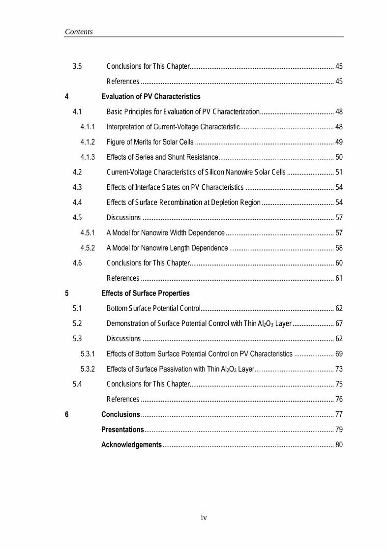
Contents
3.5 Conclusions for This Chapter ................................................................................ 45
References ........................................................................................................... 45
4.1 Basic Principles for Evaluation of PV Characterization ......................................... 48
4.2 Current-Voltage Characteristics of Silicon Nanowire Solar Cells .......................... 51
4.3 Effects of Interface States on PV Characteristics ................................................. 54
4.4 Effects of Surface Recombination at Depletion Region ........................................ 54
4.5 Discussions .......................................................................................................... 57
4.6 Conclusions for This Chapter ................................................................................ 60
References ........................................................................................................... 61
5.1 Bottom Surface Potential Control .......................................................................... 62
5.2 Demonstration of Surface Potential Control with Thin Al2O3 Layer ....................... 67
5.3 Discussions .......................................................................................................... 62
5.4 Conclusions for This Chapter ................................................................................ 75
References ........................................................................................................... 76
iv
Introductions
1
1 Introductions
This chapter overviews introductions for this thesis. The main advantages and
issues on silicon nanowire solar cells will briefly be reviewed.
1.1 Advantages of Silicon Nanowires as Solar Cell Structures
Silicon nanowires are attracting extreme interest for future building block of high
efficiency solar cells. Crystalline silicon solar cell have been running the forefront of
solar cell industries for decades, however, the conversion efficiency of crystalline
silicon is now approaching the theoretical limit of 29% [1.1]. In order to overcome this
problem, a brand new technology or structure must be established for future
improvement of solar cells.
Silicon as a solar cell material was the most common solution, however, the
potential disadvantages were lying in front of this useful material. The bandgap of is
1.12 eV which is not optimum for solar cell applications. The optimum bandgap is
known to be 1.4 eV to 1.7 eV since the solar cell spectrum includes higher intensity
around these wavelength. (See Figure. 1.2) Moreover, the band structure of crystalline
silicon is indirect bandgap which leads to a disadvantage on conversion efficiency.
From this view point, silicon nanowires are believed to have potential advantage for
solar cell application for several reasons. For further, i.e. break-through, improvement
of silicon solar cell efficiencies, the modulation of bandgap and band structure are
necessary. Figure 1.2 shows the solar spectrum and absorption wavelength for silicon
bandgap and silicon nanowire bandgap. As shown in the figure, silicon nanowires with
bandgap of ~1.5 eV enables to absorb solar energy of high intensity wavelength. Silicon

Introductions
2
nanowires are known to show bandgap enhancement in small diameters around 4 nm
owing to the quantum confinement effects [1.3]. Also the band structure changes
indirect to direct [1.4]. This is the most important advantage of silicon nanowires for
solar cell applications, and is the reason why silicon nanowires are attracting special
interest for future candidate for solar cells.
Another advantage of silicon nanowire solar cell is that they have light trapping
effects. The three-dimensional array structures trap the light inside by enhanced surface
scattering and optical confinement effect [1.5][1.6]. Owning to this enhancement of
optical characteristics, silicon nanowire cells (especially with vertical arrays) show
dramatically improved absorption efficiency compared to bulk silicon cells.
Figure 1.1 Best research-cell efficiencies for recent years. The efficiencies for crystalline
silicon cells are approaching the theoretical limit of ~29% [1.2].
Silicon
Multijunction
Thin-film
Technologies
Emerging PV
Theoretical limit of Si cells (~29 %)

Introductions
3
Figure 1.2 Spectral irradiance of sun at air mass (AM) 1.5 global conditions. The
absorption wavelength of single crystal silicon and silicon nanowire are also shown in the
figure.
Sp
ectr
al I
rrad
ianc
e (W
m-2
/nm
)
Wavelength (nm)
AM1.5 Global
0 500 1000 1500 2000 2500
0.5
1
1.5
SiNW(Eg ~ 1.5 eV)
c-Si
(Eg ~ 1.1 eV)
Figure 1.3 Light trapping effects in silicon nanowires. A drastic reduction of transmission
efficiency was observed in wafers with nanowire arrays [1.5].
Introductions
4
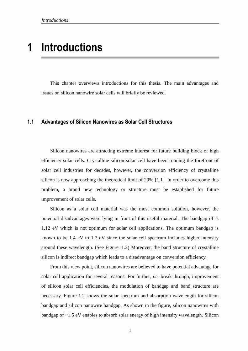
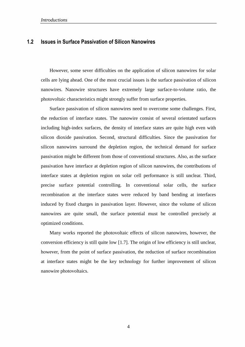
1.2 Issues in Surface Passivation of Silicon Nanowires
However, some sever difficulties on the application of silicon nanowires for solar
cells are lying ahead. One of the most crucial issues is the surface passivation of silicon
nanowires. Nanowire structures have extremely large surface-to-volume ratio, the
photovoltaic characteristics might strongly suffer from surface properties.
Surface passivation of silicon nanowires need to overcome some challenges. First,
the reduction of interface states. The nanowire consist of several orientated surfaces
including high-index surfaces, the density of interface states are quite high even with
silicon dioxide passivation. Second, structural difficulties. Since the passivation for
silicon nanowires surround the depletion region, the technical demand for surface
passivation might be different from those of conventional structures. Also, as the surface
passivation have interface at depletion region of silicon nanowires, the contributions of
interface states at depletion region on solar cell performance is still unclear. Third,
precise surface potential controlling. In conventional solar cells, the surface
recombination at the interface states were reduced by band bending at interfaces
induced by fixed charges in passivation layer. However, since the volume of silicon
nanowires are quite small, the surface potential must be controlled precisely at
optimized conditions.
Many works reported the photovoltaic effects of silicon nanowires, however, the
conversion efficiency is still quite low [1.7]. The origin of low efficiency is still unclear,
however, from the point of surface passivation, the reduction of surface recombination
at interface states might be the key technology for further improvement of silicon
nanowire photovoltaics.
Introductions
5
Figure 1.4 Schematic image of surface passivation for p-i-n silicon nanowires.
Figure 1.5 Surface recombination at interface states. Trapping of photo generated carriers
occur in depletion region of p-i-n structure.

Introductions
6
1.3 Purpose of This Thesis
From these viewpoints, this study focus on interface characterization of silicon
nanowires, evaluation of effects of interface states at depletion region on silicon
nanowire photovoltaics, and surface potential controlling of silicon nanowires to
suppress the surface recombination at interface states. The goal of this study is to clarify
the effects of interface states on silicon nanowire solar cells and propose a way to
reduce those effects with precise control of surface potential.
Figure 1.6 shows the structure tree of this thesis. This thesis
Figure 1.6 Structure tree of this thesis.
Introductions
7
References
[1.1] W. Shockley and H. J. Queisser, “Detailed Balance Limit of Efficiency of p-n
Junction Solar Cells,” J. Appl. Phys., vol. 32, 510, 1961.
[1.2] Report from National Renewable Energy Laboratory (NREL), 2013.
[1.3] H. Scheel, S. Reich, and C. Thomsen, “Electronic Band Structure of
High-Index Silicon Nanowires,” Phys. Stat. Sol. (b), vol. 242, no. 12, pp.
2474-2479, 2005.
[1.4] L. Yang, C. D. Spataru, S. G. Louie, and M. Y. Chou, “Enhanced electron-hole
interaction and optical absorption in a silicon nanowire,” Phys. Rev. B, vol. 7,
201304, 2007.
[1.5] E. Garnett and P. Yang, “Light Trapping in Silicon Nanowire Solar Cells,”
Nano Lett., vol. 10, pp. 1083-1087, 2010.
[1.6] M. D. Kelzenberg, S. W. Boettcher, J. A. Petykiewicz, D. B. Turner-Evans, M.
C. Putnam, E. L. Warren, J. M. Spurgeon, R. M. Briggs, N. S. Lewis, and H. A.
Atwater, “Enhanced absorption and carrier collection in Si wire arrays for
photovoltaic applications,” Nature Materials, vol. 9, pp. 239-244, 2010.
[1.7] T. J. Kempa, B. Tian, D. R. Kim, J. Hu, X. Zheng, and C. H. Lieber, “Single
and Tandem Axial p-i-n Nanowire Photovoltaic Devices,” Nano Lett., vol. 8,
no. 10, pp. 3456-3460, 2008.
Fabrication of Nanowire Solar Cells
8
2 Fabrication of Nanowire Solar Cells
In this chapter, methods for the fabrication of silicon nanowires solar cells will be
briefly reviewed.
2.1 Overview of Device Fabrication Procedures
Figure 2.1 shows a flow chart of process steps for p-i-n silicon nanowire diodes.
Silicon nanowires were fabricated with (100)-orientated silicon-on-insulator (SOI)
substrates on 140-nm-thick buried oxide (BOX) layer. The details of nanowire
patterning are explained in following section. Nanowires fabricated on BOX layer were
carefully cleaned with sulfuric acid (H2SO4) and hydrogen peroxide (H2O2) mixture
(SPM) followed by chemical oxide etching with 1 diluted hydrogen fluoride (HF).
Silicon nanowires were subsequently oxidized in O2 ambient at 1000C to form the
thermal oxide (SiO2) around the silicon surface. Since silicon nanowires consist of
several crystalline orientations, the thickness of thermal oxide was not uniform for
every surfaces, the actual thickness were controlled around 10 nm to 25 nm, and the
corners had the thinnest. The thickness of thermal oxide was not so important in this
study, the only limitation for the thickness was sufficient for prevent the gate leakage
current for gated diodes, and for surface passivation of silicon surfaces.
The junction for p-i-n diode structure was formed by ion implantation of P+ ion and
BF2+ ion for cathode and anode, respectively. The gas sources were phosphine (PH3)
and boron trifluoride (BF3). Each of the ions was accelerated from 20 kV to 30 kV

Fabrication of Nanowire Solar Cells
9
depending on the thickness of thermal oxide and the residual thickness of SOI layers.
The implanted ions were then activated in N2 ambient at 800C for 30 minutes. After
configuring the anode and cathode regions, 50-nm-thick titanium nitride (TiN) gate
electrode was deposited by radio frequency (RF) magnetron sputtering technique for
gated diodes used in interface characterizations. Note that the deposition of gate
electrode was omitted for the solar cells fabrication. Thermal dioxide at the both ends of
silicon nanowires were removed with buffered hydrogen fluoride (BHF) solution, and
60-nm-thick aluminum (Al) contact electrodes were deposited by RF magnetron
sputtering. 50-nm-thick Al back side electrode was deposited by thermal evaporation
technique, and the substrates were annealed in forming gas (FG), mixture of 3 H2 and
97 N2 gas, at 420C for 30 minutes for the H-termination of dangling bonds. Note that
all the measurements were conducted at room temperature conditions (𝑇 = 300 [K]).
Figure 2.2 shows schematic image of device structure, SEM image of the device, and
cross-sectional TEM image of a nanowire. Note that the silicon nanowires were
connected in parallel.

Fabrication of Nanowire Solar Cells
10
Figure 2.1 Flow chart of process steps for (gated) p-i-n diodes fabricated on
silicon-on-insulator substrates.

Fabrication of Nanowire Solar Cells
11
(a) (b)
(c)
(d)
Figure 2.2 Structure of silicon nanowire solar cells. (a) Top view of one device fabricated
on a silicon-on-insulator substrate. A hundred nanowires are electrically connected in parallel.
Cross section view of (b) Y-Y’ direction and (c) X-X’ direction. (d) SEM image of the silicon
nanowire solar cells and cross-section TEM image of a nanowire.
BOX
X X
Y
Y
100 nanowires in parallel
BOX
Si
Thermal oxide
p-Si substrate (800 m)
BOX layer (145 nm)
p+ n+
Vsub
(Normally grounded)
Solar simulator
(AM1.5 G, 100 mW/cm2)
Thermal oxide (10~20 nm)
Silicon nanowire
(Thickness: 12~42 nm)
Aluminum contact (~80 nm)
Aluminum back contact (50 nm)
p i n
10 m 1 m
Top
Sid
e
SiO2
BOX
Sid
eSi

Fabrication of Nanowire Solar Cells
12
2.2 Details of Key Steps
2.2.1 Pattering of Silicon Nanowire
Figure 2.3 shows schematic illustrations of silicon nanowire pattering steps. In this
work, three different substrates with SOI thickness of 30, 50, and 60 nm were used.
Silicon nanowires were fabricated with 30-nm-thick and 50-nm-thick SOI substrates,
and 60-nm-thick SOI substrates were used for planar devices as references for
characterization. SiN hard mask was deposited on carefully cleaned SOI substrates, and
patterned in line and spaces. Then the SOI layer was etched by reactive ion etching
(RIE), and SiN hard masks were removed at last. Note that BOX layer was over etched
during the silicon nanowire patterning in order to obtain sharp bottom edges (Figure
2.4). The width of silicon nanowires after SiN hard mask removal was measured with
scanning electron microscope (SEM). Nanowires on 30-nm-thick SOI substrates varied
from 40 nm to 160 nm and nanowires on 50-nm-thick SOI substrates varied from 45 nm
to 170 nm, respectively. Measure width was plotted against sample ID numbers in
Figure 2.5.
Figure 2.3 Schematic illustrations of silicon nanowire pattering steps.

Fabrication of Nanowire Solar Cells
13
Figure 2.4 Effects of over etching on sharpness of silicon nanowire bottom edges.
Figure 2.5 Width of silicon nanowires against sample ID numbers. Width were measured
with scanning electron microscope (SEM) after SiN hard mask removal.

Fabrication of Nanowire Solar Cells
14
2.2.2 Surface Passivation
Surface passivation, the main topic of this study, was performed by three different
techniques. Thermal oxidation was the most common process for surface passivation
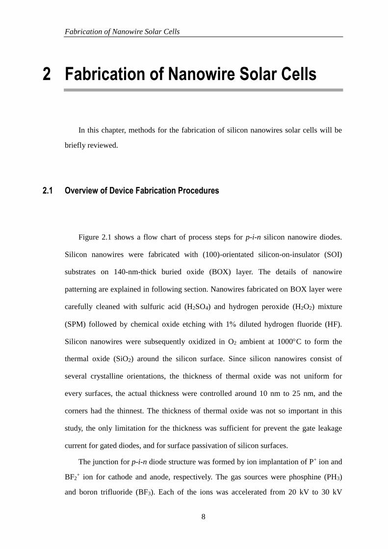
Figure 2.6 shows the thermal oxide thickness for silicon with various crystalline
orientations. Each of the silicon substrates was oxidized in O2 atmosphere with a flow
of 1 L/min at 1000C. Thermal oxide is known as a high quality interface with silicon
which provides a low interface state density (Dit) and a low fixed charge density with
optimized oxidation temperature [2.1]-[2.4]. The interface states exist between
conduction band and valance band of silicon, i.e. bandgap of silicon, and they act as
surface recombination centers, Dit at silicon nanowire/surface passivation interface must
be suppressed as low as possible to improve the photo conversion efficiency. From this
aspect, thermal oxide was adopted for all the first layer passivation of silicon nanowires,
and other passivation materials were subsequently deposited on thermal oxides.
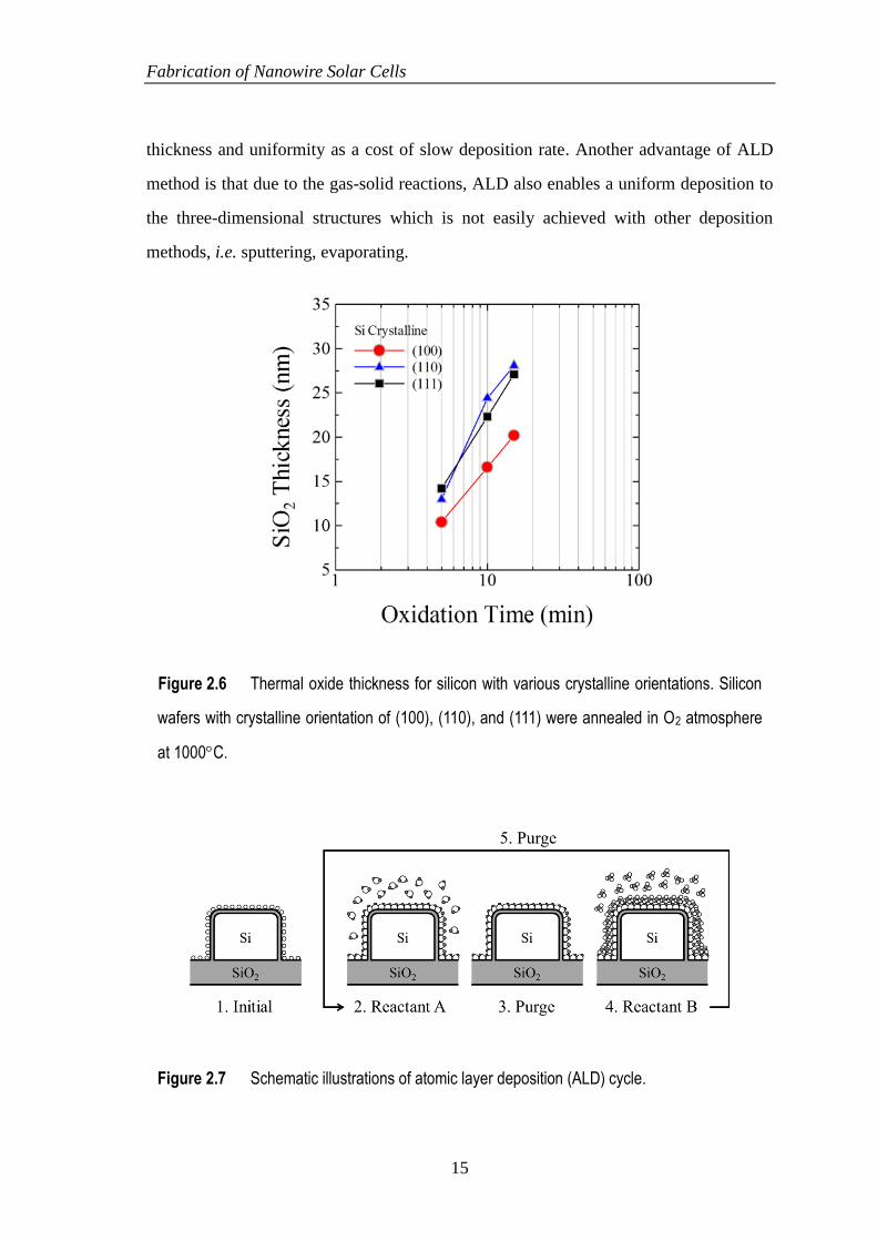
Another technique for the surface passivation of silicon nanowires were atomic
layer deposition (ALD) method [2.5][2.6]. ALD method is a deposition technique based
on the reaction between surface of substrate and precursor gas of intended materials. A
sequential use of self-terminating gas-solid reactions, as schematically shown in Figure
2.7, is the important point of ALD cycle. The ALD method consists of following four
steps:
1. Initial substrate.
2. First self-terminating reaction by Reactant A
3. Purge with inert gas (Ar) and vacuuming.
4. Second self-terminating reaction by Reactant B
5. Purge with inert gas (Ar) and vacuuming. (Return to the step #2)
Since the ALD method based on self-terminating process, only one cycle of ALD
provides one atomic layer of intent material which enables a precise control of material
Fabrication of Nanowire Solar Cells
15
thickness and uniformity as a cost of slow deposition rate. Another advantage of ALD
method is that due to the gas-solid reactions, ALD also enables a uniform deposition to
the three-dimensional structures which is not easily achieved with other deposition
methods, i.e. sputtering, evaporating.
Figure 2.6 Thermal oxide thickness for silicon with various crystalline orientations. Silicon
wafers with crystalline orientation of (100), (110), and (111) were annealed in O2 atmosphere
at 1000C.
Figure 2.7 Schematic illustrations of atomic layer deposition (ALD) cycle.

Fabrication of Nanowire Solar Cells
16
2.2.3 Junction Formation
Junction formation is one of the most important issues for the improvement of
nanowire devices. Since the nanowires have quite small volume and cross section, the
existence of large series resistance is a crucial problem for any nanowire devices. To
overcome this disadvantage of nanowire structures, many technologies were introduced
by previous works.
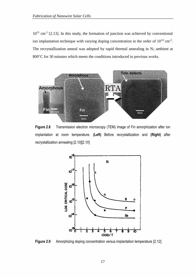
Ion implantation is the most common technology for the junction formation of
conventional planar devices due to its reliability, usefulness, and controllability.
However, the problem of ion implantation to semiconductors are the interfacial
amorphization of material crystalline structures which was conventionally overcame by
recrystallization with post annealing at high temperature [2.7][2.8]. For conventional
planar devices, the recrystallization of interfacial amorphous layer was achieved due to
the crystalline matching of substrate, in other words, the substrate acted as a seed of
original crystalline orientation. For three-dimensional channel devices, i.e. fins and
nanowires, the amorphization of interfacial layer was proved to be a more grave issue
because there are more damage to the material crystalline at the corners of
three-dimensional structures due to the angled implantation for sidewalls [2.9][2.10].
This amorphization causes increase in series resistance and variability in device
performance which degrades the device reliability. Considering the solar cell
applications, defects induced by this amorphization will be a recombination center and
lifetime killer of photo-generated carriers. Since the nanowires are a small volume
structure, the doping concentration is also an important parameter to optimized junction
formation. Many of the studies on ion implantation damage showed that amorphization
of silicon crystalline relates to both doping concentration and implantation temperature
[2.11][2.12]. Colli, et al. investigated the ion implantation into silicon nanowire with
varying the doping concentration, and concluded that full recrystallization of crystalline
silicon nanowires can be achieved by annealing at 800C for doping concentration upto
Fabrication of Nanowire Solar Cells
17
1015 cm-2 [2.13]. In this study, the formation of junction was achieved by conventional
ion implantation technique with varying doping concentration in the order of 1014 cm-2.
The recrystallization anneal was adopted by rapid thermal annealing in N2 ambient at
800C for 30 minutes which meets the conditions introduced in previous works.
Figure 2.8 Transmission electron microscopy (TEM) image of Fin amorphization after ion
implantation at room temperature. (Left) Before recrystallization and (Right) after
recrystallization annealing [2.10][2.10]
Figure 2.9 Amorphizing doping concentration versus implantation temperature [2.12].
Fabrication of Nanowire Solar Cells
18
Epitaxial growth of doped silicon is also an effective way to form the junction to
three dimensional structures. Devices using this technique for source and drain regions
reported high performance electric characteristics even in extremely scaled sizes
[2.14][2.15]. This technique enables a uniform junction formation independent of
nanowire sizes, however, there are many fabrication process difficulties in order to
adopt, and the minority carrier lifetime might be shorter due to its low crystalline
orientation. The other way to collect the carriers are to form a Schottky barrier contact
at each ends of nanowires. Schottky barrier diode enables rectification without ion
implantation and subsequent high temperature post annealing process which degrades
the carrier lifetimes. However, since the suppression of metal diffusion into nanowires
and highly transparence of top contact electrode are both necessary for solar cell
applications, there lies the difficulties in selection of contact material.
Another important point for junction formation is the thickness optimization of
depletion region. The p-i-n diode is a special case of p-n diode which has an intrinsic (or
slightly doped) region between p-n junctions. Figure 2.10 shows a schematic illustration
of carrier transport for each type of junction.

Fabrication of Nanowire Solar Cells
19
2.2.4 Hydrogen Termination of Interface States
The origin of interface states interface were known to be the existence of structural
defects, oxidation-induced defects, metal impurities, or defects induced by bond
breaking processes such as radiation or hot electron injections. The defect bonds, e.g.
dangling bonds, which are the most major component of interface states can be
neutralized by low-temperature annealing in hydrogen or hydrogen/nitrogen mixture
(forming gas). The hydrogen termination of dangling bonds at silicon/thermal oxide
interface was studied in detail by previous works, and it is well understood that the
density of interface state strongly correlates to the crystalline orientation of silicon
substrate underlying the thermal oxide [2.16][2.17]. For silicon/thermal oxide interface
of silicon nanowires, the density of interface states are known to be higher than the
planar silicon substrates due to the existence of high-index orientation sidewalls and
corners [2.18]. The hydrogen termination is still effective approach for the
Figure 2.10 Schematic illustrations of (a) p-n junction and (b) p-i-n junction solar cells. p-i-n
junction solar cell is a special case of p-n junction solar cell which has an optimized depletion
region thickness and current dominated by drift component.

Fabrication of Nanowire Solar Cells
20
neutralization of dangling bonds of silicon nanowires consistent with the planar silicon
[2.19]. In this work, the hydrogen termination was conducted by forming gas annealing
in forming gas at 420C for 30 minutes. (See Figure 2.11)
Figure 2.11 Changes in interface state distribution at silicon nanowire/thermal oxide
interface with various forming gas annealing temperature [2.19].
Fabrication of Nanowire Solar Cells
21
References
[2.1] A. S. Grove, B. E. Deal, E. H. Snow, and C. T. Sah, “Investigation of
Thermally Oxidised Silicon Surfaces Using Metal-Oxide-Semiconductor
Structures,” Solid-State Electron., vol. 8, pp. 145-163, 1965.
[2.2] B. E. Deal and A. S. Grove, “General Relationship for the Thermal Oxidation
of Silicon,” J. Appl. Phys., vol. 36, pp. 3770-3778, 1965.
[2.3] B. E. Deal, A. S. Grove, and E. H. Snow, “Characteristics of the Surface-State
Charge (Qss) of Thermally Oxidized Silicon,” J. Electrochem. Soc., vol. 114, no.
3, pp. 266-274, 1967.
[2.4] R. R. Razouk and B. E. Deal, “Dependence of Interface State Density on
Silicon Thermal Oxidation Process Variables,” J. Electrochem. Soc., vol. 126,
no. 9, pp. 1573-1581, 1979.
[2.5] S. M. George, “Atomic Layer Deposition: An Overview,” Chem. Rev., vol. 110,
pp. 111-131, 2010.
[2.6] R. L. Puurunen, “Surface Chemistry of Atomic Layer Deposition: A Case
Study for the trimethylaluminum/water process,” J. Appl. Phys., vol. 97,
121301, 2005.
[2.7] T. Henkel, V. Heera, R. Kögler, W. Skorupa, and M. Seibt, “Kinetics of
Ion-Beam-Induced Interfacial Amorphization in Silicon,” J. Appl. Phys., vol.
82, 5360, 1997.
[2.8] L. Pelaz, L. A. Marqués, and J. Barbolla, “Ion-Beam-Induced Amorphization
and Recrystallization in Silicon,” J. Appl. Phys., vol. 96, 5947, 2004.

Fabrication of Nanowire Solar Cells
22
[2.9] R. Duffy, G. Curatola, B. J. Pawlak, G. Doornbos, K. van der Tak, P. Breimer, J.
G. M. van Berkum, and F. Roozeboom, “Doping Fin Field-Effect Transistor
Sidewalls: Impurity Dose Retention in Silicon Due to High Angle Incident Ion
Implants and the Impact on Device Performance,” J. Vac. Sci. Technol. B, vol.
26, pp. 402-407, 2008.
[2.10] M. Togo, Y. Sasaki, G. Zschätzsch1, G. Boccardi, R. Ritzenthaler, J. W. Lee, F.
Khaja, B. Colombeau, L. Godet, P. Martin, S. Brus, S. E. Altamirano, G.
Mannaert, H. Dekkers, G. Hellings, N. Horiguchi, W. Vandervorst, and A.
Thean, “Heated Implantation with Amorphous Carbon CMOS Mask for Scaled
FinFETs,” VLSI Tech. Symp. Dig., pp. 196-197, 2013.
[2.11] F. F. Morehead, B. L. Crowder, and R. S. Title, “Formation of Amorphous
Silicon by Ion Bombardment as a Function of Ion, Temperature, and Dose,” J.
Appl. Phys., vol. 43, pp. 1112-1118, 1972.
[2.12] J. F. Gibbsons, “Ion Implantation in Semiconductors – Part II: Damage
Production and Annealing,” Proc. IEEE, vol. 60, no. 9, pp. 1062-1096, 1972.
[2.13] A. Colli, A. Fasoli, C. Ronning, S. Pisana, S. Piscanec, and A. C. Ferrari, “Ion
Beam Doping of Silicon Nanowires,” Nano Lett., vol. 8, no. 8, pp. 2188-2193,
2008.
[2.14] J. R. Pfiester, R. D. Sivan, H. M. Liaw, C. A. Seelbach, and C. D. Gunderson,
“A Self-Aligned Elevated Source/Drain MOSFET,” IEEE Electron. Device
Lett., vol. 11, no. 9, pp. 365-367, 1990.
[2.15] S. Bangsaruntip, K. Balakrishnan, S.-L. Cheng, J. Chang, M. Brink, I. Lauer, R.
L. Bruce, S. U. Engelmann, A. Pyzyna, G. M. Cohen, L. M. Gignac, C. M.
Breslin, J. S. Newbury, D. P. Klaus, A. Majumdar, J. W. Sleight and M. A.
Fabrication of Nanowire Solar Cells
23
Guillorn, “Density Scaling with Gate-All-Around Silicon Nanowire MOSFETs
for the 10 nm node and beyond,” IEDM Tech. Dig., pp.526-529, 2013.
[2.16] B. E. Deal, E. L. MacKenna, and P. L. Castro, “Characteristics of Fast Surface
States Associated with SiO2-Si and Si3N4-SiO2-Si Structures,” J. Electrochem.
Soc., vol. 116, no.7, pp. 997-1005, 1969.
[2.17] M. L. Reed and J. D. Plummer, “Chemistry of Si-SiO2 Interface Trap
Annealing,” J. Appl. Phys., vol. 63, pp. 5776-5793.
[2.18] G. Kapila, B. Kaczer, A. Nackaerts, N. Collaert, and G. V. Groeseneken,
“Direct Measurement of Top and Sidewall Interface Trap Density in SOI
FinFETs,” IEEE Trans. Electron Devices, vol. 28, no. 3, pp. 232-234, 2007.
[2.19] K. Nakajima, “Interface-state Density of Three Dimensional Silicon Channels
Measured by Charge Pumping Method,” Master Thesis, 2012.
Evaluation of Interface States
24
3 Evaluation of Interface States
As introduced in Chapter 1, interface states must be reduced in order to maximize
the efficiency since they act as recombination centers for the photo-generated carriers.
This chapter explains results from the evaluation of interface states at silicon nanowire
surface by charge pumping technique. Gate electrodes formed on silicon nanowire solar
cells were used to characterize the interface states electrically. Starting from a brief
explanation of charge pumping technique modulated for gated diodes, the results from
the charge pumping measurements with silicon nanowire solar cells with various
nanowire sizes will be discussed.
3.1 Basic Principles in Charge Pumping Technique
3.1.1 Explanation of Conventional Method for MOS Structures
Several techniques have been proposed for the determination of the surface states.
Most of common techniques, i.e. capacitance-voltage (C-V) technique and conductance
technique, were basically applicable for metal-oxide-semiconductor (MOS) structures
[3.1]-[3.4]. For MOS transistors, subthreshold current technique [3.5], deep-level
transient spectroscopy (DLTS) [3.6], direct-current current-voltage (DC-IV)
measurement technique [3.7], and charge pumping technique were commonly adopted
[3.8]. In this section, the basic principles of charge pumping technique are reviewed
briefly. The main advantage of charge pumping technique is that it enables direct
measurement of surface states with only preparing additional gate electrode on p-i-n
diode structures, i.e. solar cells.
Evaluation of Interface States
25
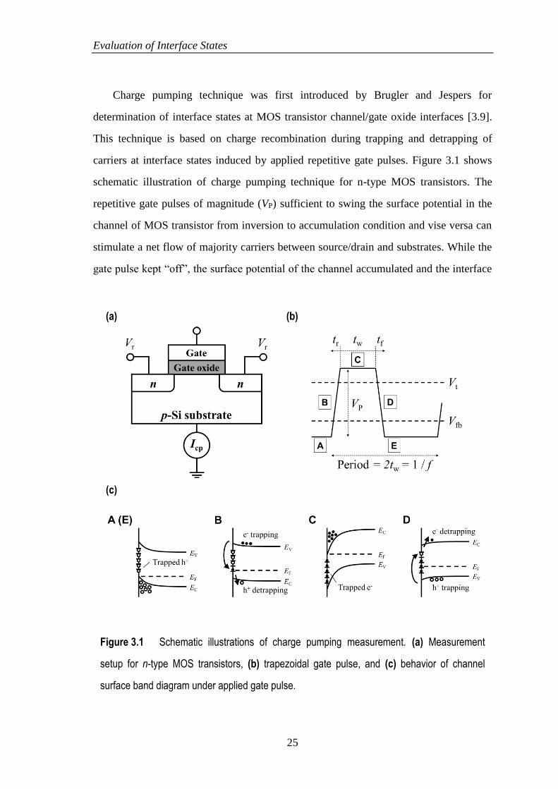
Charge pumping technique was first introduced by Brugler and Jespers for
determination of interface states at MOS transistor channel/gate oxide interfaces [3.9].
This technique is based on charge recombination during trapping and detrapping of
carriers at interface states induced by applied repetitive gate pulses. Figure 3.1 shows
schematic illustration of charge pumping technique for n-type MOS transistors. The
repetitive gate pulses of magnitude (VP) sufficient to swing the surface potential in the
channel of MOS transistor from inversion to accumulation condition and vise versa can
stimulate a net flow of majority carriers between source/drain and substrates. While the
gate pulse kept “off”, the surface potential of the channel accumulated and the interface
(a) (b)
(c)
Figure 3.1 Schematic illustrations of charge pumping measurement. (a) Measurement
setup for n-type MOS transistors, (b) trapezoidal gate pulse, and (c) behavior of channel
surface band diagram under applied gate pulse.

Evaluation of Interface States
26
states were subsequently filled with holes flew from substrate. On the other hand, the
interface states were filled with electrons flew from source/drain region while the gate
pulse kept “on”. Pulse duration (tw) and pulse period (1 𝑓⁄ ) should be taken sufficiently
long to assure all the surface states are filled with electrons or holes [3.8]. Since the
carrier recombination occur only when trapped holes (electrons) remain at the interface
states and capture of electrons (holes) subsequently take place, the important process in
charge pumping technique happens during transition of gate pulse from “on” to “off”
and vise versa. Because the electrons trapped at states near the conduction band or holes
trapped at near the valence band will detrap to each band during the pulse transition,
keeping the gate pulse transition time (tr, tf) short is important for accurate measurement
of interface state density.
To improve the accuracy of charge pumping, the use of offset voltage (Vbase) for
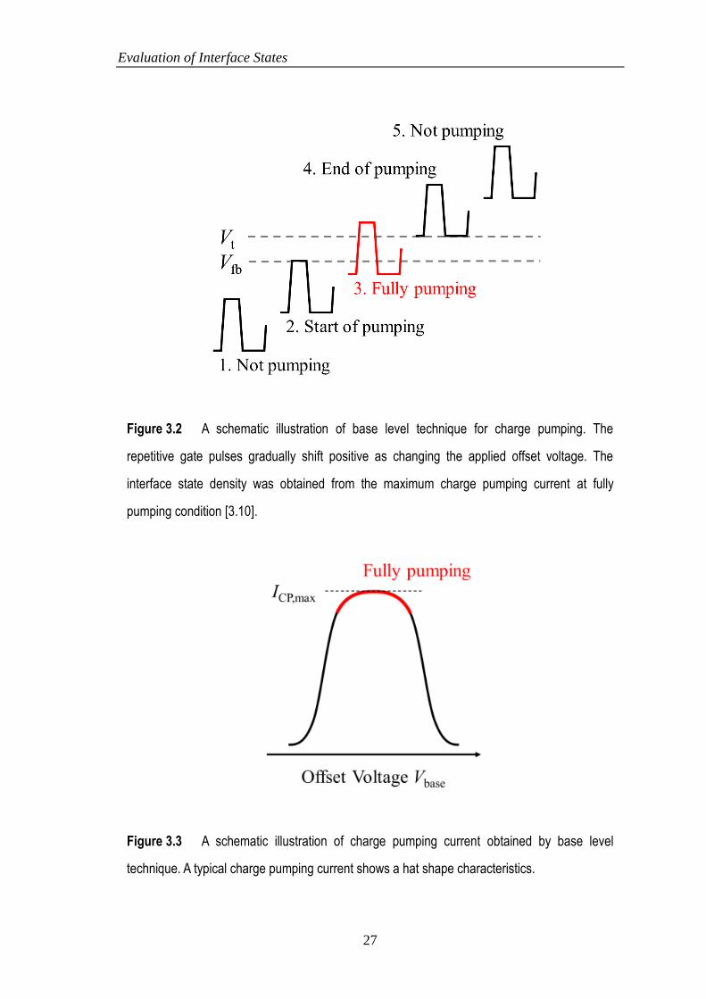
gate pulse called base level technique was proposed by Elliot [3.10]. A schematic
illustration of base level technique is shown in Figure 3.2. The repetitive gate pulses
gradually shift positive as changing the applied offset voltage, and the interface state
density was obtained by taking the charge pumping current at fully pumping condition.
At fully pumping conditions, the surface potential of channel was sufficiently inverted
or accumulated and interface states were completely trapped by electrons or holes. By
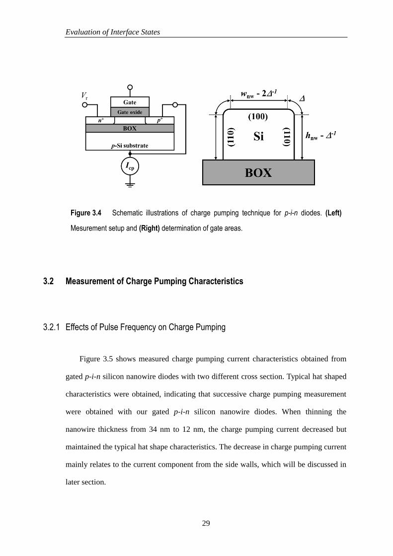
measuring the charge pumping current while changing the offset voltage, the maximum
current (ICP,max) will be obtained during the fully pumping conditions so that a typical
charge pumping current shows a hat shaped characteristics as schematically shown in
Figure 3.3. From the measured ICP,max, the average of interface state density (Dit) can be
expressed as follows,
𝐷it = 𝑞𝑓𝐴G𝐼CP,max, (3.1)
where q, f, and AG are the electron charge, gate pulse frequency, and surface area of the
channel.
Evaluation of Interface States
27
Figure 3.2 A schematic illustration of base level technique for charge pumping. The
repetitive gate pulses gradually shift positive as changing the applied offset voltage. The
interface state density was obtained from the maximum charge pumping current at fully
pumping condition [3.10].
Figure 3.3 A schematic illustration of charge pumping current obtained by base level
technique. A typical charge pumping current shows a hat shape characteristics.

Evaluation of Interface States
28
As shown in the Figure 3.2, the rising voltage and falling voltage of charge
pumping current are strongly related with threshold voltage and flatband voltage,
respectively. However, the value change with gate pulse magnitude, so the detailed
explanation of threshold voltage or flatband voltage need other characterization
technique to be adopted, for example, capacitance-voltage measurement.
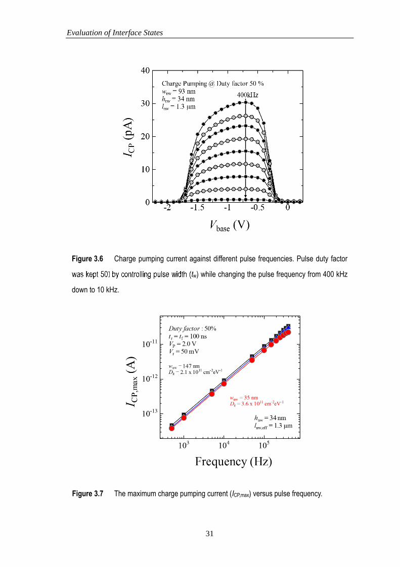
3.1.2 Modified Charge Pumping Technique for Gated Diodes
Measurement of interface state density in silicon nanowire diodes with charge
pumping technique was first reported by Kapila [3.11]. Since our silicon nanowire
diodes were fabricated with SOI substrates, the charge pumping current won’t flow
through the substrate so current must be able to measure at one of the two ends of
silicon nanowires. From this point, silicon nanowires must be prepared with a p-i-n
diode rather than a transistor structure. The measurement setups for p-i-n diode structure
prepared on SOI substrate are shown in Figure 3.4. In this setup, charge pumping
current was measured at p+-type end of silicon nanowire and also from the substrate to
monitor the leakage current through the BOX layer. Since the cross section of silicon
nanowire consist of four different surfaces, i.e. top, side, corner, and bottom, the area of
gated region can be expressed as follows,
𝐴G = 𝐴top + 2𝐴side + 2𝐴corner + 𝐴bottom, (3.2)
where Atop, Aside, Acorner, and Abottom are the area of top, side corner, and bottom surface
respectively. Note that Abottom can be neglected throughout the measurement because the
gate electrode was not prepared with gate-all-around structure.
Evaluation of Interface States
29
3.2 Measurement of Charge Pumping Characteristics
3.2.1 Effects of Pulse Frequency on Charge Pumping
Figure 3.5 shows measured charge pumping current characteristics obtained from
gated p-i-n silicon nanowire diodes with two different cross section. Typical hat shaped
characteristics were obtained, indicating that successive charge pumping measurement
were obtained with our gated p-i-n silicon nanowire diodes. When thinning the
nanowire thickness from 34 nm to 12 nm, the charge pumping current decreased but
maintained the typical hat shape characteristics. The decrease in charge pumping current
mainly relates to the current component from the side walls, which will be discussed in
later section.
Figure 3.4 Schematic illustrations of charge pumping technique for p-i-n diodes. (Left)
Mesurement setup and (Right) determination of gate areas.

Evaluation of Interface States
30
Figure 3.6 shows the changes in charge pumping current against different pulse
frequencies. Note that pulse duty factor was kept to be 50 by controlling the pulse
width (tw) while changing the pulse frequency. As shown in the figure, charge pumping
current clearly decreased with decreasing the pulse frequency. Figure 3.7 shows the plot
of maximum charge pumping current against different pulse frequency. Since the
relationship between charge pumping current and pulse frequency is given by Eq. (3.1),
the proportional relationship between the maximum charge pumping current and the
pulse frequency, as shown in the figure, is consistent with the principle of charge
pumping method. This proportional relationship can also be seen when varying the
nanowire width. These results assure the measurement of nanowire width dependence as
described in following section. In following measurements, pulse frequency was chosen
as 10 kHz from the proportional region.
Figure 3.5 Charge pumping current measured with gated p-i-n silicon nanowire diode with
two different nanowire cross sections. TEM images of each nanowire are also shown.
Evaluation of Interface States
31
Figure 3.6 Charge pumping current against different pulse frequencies. Pulse duty factor
tw) while changing the pulse frequency from 400 kHz
down to 10 kHz.
Figure 3.7 The maximum charge pumping current (ICP,max) versus pulse frequency.

Evaluation of Interface States
32
3.2.2 Determination of Undoped Nanowire Region Length
Figure 3.8 shows the changes in maximum charge pumpimg current (ICP,max) against
depletion region length with three different nanowire width. ICP,max for each nanowire
were plotted against nanowire length in Figure 3.9. ICP,max proportionally decreased as
depletion region shortened indicating that the surface of silicon nanowires can be
assumed to be uniform independent of their length. The linear fitting results, as shown
in the figure with dashed lines, had the same x-axis intercept at around 230 nm. Figure
3.10 describes the method for estimation of actual depletion region length from
measured data. In this study, photolithography process was used for mask pattering of
ion implantation, and there are some artificial mask alignment errors. Since the actual
Figure 3.8 Changes in charge pumping current against different nanowire length for
nanowire cross section of 34 x 85 nm2. Current decreased as nanowire length shortened.

Evaluation of Interface States
33
Figure 3.9 Changes in maximum charge pumping current against different nanowire
length. Current decreased as nanowire length shortened.
Figure 3.10 A Schematic illustration for estimation method of actual depletion region length.

Evaluation of Interface States
34
length of depletion region is necessary in order to calculate the density of interface
states, we have to estimate the actual length from the measured data. As described
before, the linear fitting of measured data in Figure 3.9 showed the same x-axis
intercepts. If there are no alignment errors for photolithography processes, the x-axis
intercepts should be zero which means the charge pumping current should be zero when
there is no undoped depletion region under the gate electrodes. From this assumption,
the value of x-axis intercept can be interpreted as the alignment error of
photolithography process for the patterning of ion implantation masks. By taking the
differential of mask designs and obtained alignment errors, the actual length of undoped
depletion region can be estimated from the measured data. This estimation was used for
all the devices in this work, and obtained actual length was used in order to calculate the
density of interface states.
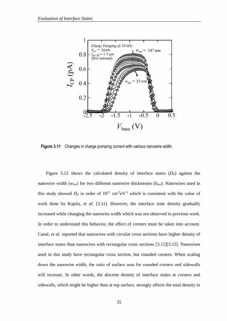
3.2.3 Effects of Nanowire Narrowing on Density of Interface States
Figure 3.11 shows the changes in charge pumping current when varying nanowire
width from 147 nm to 35 nm. Gradual decrease of the charge pumping current was
observed, and the rising and falling voltage both shifted positive as decreasing the
nanowire width. The positive shifts of rising and falling voltage indicating the threshold
voltage and flatband voltage changed when decreased the nanowire width, respectively.
Although the detailed analysis of this voltage shift should adopt other characterizing
technique as described in previous section, it should be noted that this behavior might
due to the effects of fixed charges in thermal oxide layer and more strongly affect the
surface properties in thinner nanowires.
Evaluation of Interface States
35
Figure 3.12 shows the calculated density of interface states (Dit) against the
nanowire width (wnw) for two different nanowire thicknesses (hnw). Nanowires used in
this study showed Dit in order of 1011 cm-2eV-1 which is consistent with the value of
work done by Kapila, et al. [3.11]. However, the interface state density gradually
increased while changing the nanowire width which was not observed in previous work.
In order to understand this behavior, the effect of corners must be taken into account.
Cassé, et al. reported that nanowires with circular cross sections have higher density of
interface states than nanowires with rectangular cross sections [3.12][3.12]. Nanowires
used in this study have rectangular cross section, but rounded corners. When scaling
down the nanowire width, the ratio of surface area for rounded corners and sidewalls
will increase. In other words, the discrete density of interface states at corners and
sidewalls, which might be higher than at top surface, strongly affects the total density in
Figure 3.11 Changes in charge pumping current with various nanowire width.

Evaluation of Interface States
36
smaller nanowires. In order to verify this assumptions, extraction of discrete density by
using simple model will be discussed in next section.
Figure 3.12 Density of interface states (Dit) against nanowire width (wnw). Opened circles
represent data from 12-nm-thick nanowires and closed rectangles represent data from
34-nm-thick nanowires, respectively.

Evaluation of Interface States
37
(a)
(b)
Figure 3.13 (a)(b) Energy distribution of density of interface states for planar SOI transistor,
rectangular nanowire transistor, and circular nanowire transistor. Nanowires with circular cross
section showed higher density [3.12].
Evaluation of Interface States
38
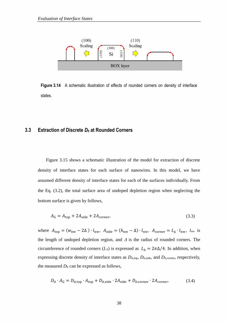
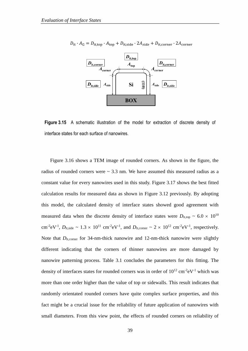
3.3 Extraction of Discrete Dit at Rounded Corners
Figure 3.15 shows a schematic illustration of the model for extraction of discrete
density of interface states for each surface of nanowires. In this model, we have
assumed different density of interface states for each of the surfaces individually. From
the Eq. (3.2), the total surface area of undoped depletion region when neglecting the
bottom surface is given by follows,
𝐴G = 𝐴top + 2𝐴side + 2𝐴corner, (3.3)
where 𝐴top = (𝑤nw − 2∆ ) ∙ 𝑙nw, 𝐴side = (ℎnw − ∆) ∙ 𝑙nw, 𝐴corner = 𝐿∆ ∙ 𝑙nw , lnw is
the length of undoped depletion region, and is the radius of rounded corners. The
circumference of rounded corners (L) is expressed as 𝐿∆ = 2𝜋∆ 4⁄ . In addition, when
expressing discrete density of interface states as Dit,top, Dit,side, and Dit,corner, respectively,
the measured Dit can be expressed as follows,
𝐷it ∙ 𝐴G = 𝐷it,top ∙ 𝐴top + 𝐷it,side ∙ 2𝐴side + 𝐷it,corner ∙ 2𝐴corner. (3.4)
Figure 3.14 A schematic illustration of effects of rounded corners on density of interface
states.
Evaluation of Interface States
39
Figure 3.16 shows a TEM image of rounded corners. As shown in the figure, the
radius of rounded corners were ~ 3.3 nm. We have assumed this measured radius as a
constant value for every nanowires used in this study. Figure 3.17 shows the best fitted
calculation results for measured data as shown in Figure 3.12 previously. By adopting
this model, the calculated density of interface states showed good agreement with
measured data when the discrete density of interface states were Dit,top ~ 6.0 1010
cm-2eV-1, Dit,side ~ 1.3 1011 cm-2eV-1, and Dit,corner ~ 2 1012 cm-2eV-1, respectively.
Note that Dit,corner for 34-nm-thick nanowire and 12-nm-thick nanowire were slightly
different indicating that the corners of thinner nanowires are more damaged by
nanowire patterning process. Table 3.1 concludes the parameters for this fitting. The
density of interfaces states for rounded corners was in order of 1012 cm-2eV-1 which was
more than one order higher than the value of top or sidewalls. This result indicates that
randomly orientated rounded corners have quite complex surface properties, and this
fact might be a crucial issue for the reliability of future application of nanowires with
small diameters. From this view point, the effects of rounded corners on reliability of
Figure 3.15 A schematic illustration of the model for extraction of discrete density of
interface states for each surface of nanowires.

Evaluation of Interface States
40
surface passivation for silicon nanowires will be discuss in following section.
Figure 3.16 Transmission Electron Microscopy (TEM) image of rounded corner. The radius
of corners was ~ 3.3 nm.
Figure 3.17 Fitted calculation results on measured data shown in Figure 3.12. The
calculation results best fitted with parameters shown in Table 3.1.
Evaluation of Interface States
41
3.4 Effects of Corners on Surface Passivation Reliability
In order to characterize the effects of rounded corners on the reliability of surface
passivation, Fowler-Nordheim (FN) injection was adopted to the gated p-i-n silicon
nanowire diodes. Figure 3.18 shows a schematic illustration of FN injection on gated
p-i-n diode structure. As described in the figure, positive bias was applied to the gate
electrode in order to inject electrons into the thermal oxide while cathode electrode was
grounded. On the other hand, negative bias was applied to the gate electrode to inject
holes while anode electrode was grounded. Charge pumping measurement was
subsequently conducted after the carrier injection in order to monitor the generation of
defects or interface states. From the time evolution of interface state generation for
various nanowire cross sections, the reliability of surface passivation of silicon
nanowires can be characterized.
Table 3.1 Parameters for extraction of discrete density of interface states used in Figure
3.17.

Evaluation of Interface States
42
Changes in charge pumping current under high-field FN injection with nanowire
cross section of 93 34 nm2 are shown in Figure 3.19. Positive bias of 10 V was
applied to gate electrode while cathode grounded, and the changes in charge pumping
current was monitored. Charge pumping current clearly increased more than one order
higher indicating that interface states were generated under FN injection. Note that
contributions of injected electrons into SiO2 layers to charge pumping current were
negligible since the shifts in Vt or Vfb, as explained in previous section, were quite small
even after 100 second of FN injection.
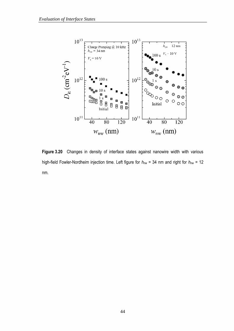
Time evolution of density of interface states under FN injection with varying
nanowire cross section are shown in Figure 3.19. Interface states for nanowires with
cross section of 30 12 nm2 increased rapid than others, almost one order higher after
100 second injection, while nanowires with largest cross section (134 34 nm2) only
doubled. Figure 3.20 shows the changes in density of interface states against nanowire
width with varying stressing time. Interface states clearly increased with keeping the
same trend of before injecting electrons, however seen at data of 1 second injection
(light gray in the figure), increase in thinner nanowires (hnw = 12 nm) were quite large
Figure 3.18 A schematic illustration of Fowler-Nordheim (FN) injection on gated p-i-n
diodes. (a) Electron injection and (b) hole injection into the gate oxide.

Evaluation of Interface States
43
while slightly increased in thicker nanowires. These results indicating that the ratio of
corners severely affect the stability of surface passivation.
Figure 3.19 Time evolution of density of interface states under high-field Fowler-Nordheim
injection. Nanowires with smallest cross section increased rapidly.
Evaluation of Interface States
44
Figure 3.20 Changes in density of interface states against nanowire width with various
high-field Fowler-Nordheim injection time. Left figure for hnw = 34 nm and right for hnw = 12
nm.

Evaluation of Interface States
45
3.5 Conclusions for This Chapter
In this section, the interface states at silicon nanowire/thermal oxide interface were
characterized by adopting gated p-i-n silicon nanowire diodes. Charge pumping method
was adopted for the measurement of density of interface states.
From the measurement of different cross section nanowires, the effects of rounded
corners on density of interface states were extracted. By assuming discrete density for
top, sidewalls, and corners individually, the extracted density for rounded corners were
in order of 1012 cm-2eV-1 which was more than one order higher than other flat surfaces.
This results indicating that the management of rounded corners is especially important
issue for the reduction of interface states for future scaling down of nanowire diameters.
From the point of reduction of interface states, nanowires with rectangular like cross
section can be a promising candidate for future nanowire applications.
Although, the effects of rounded corners on the reliability of surface passivation of
nanowires were characterized by adopting Fowler-Nordheim injection method. After
electron injection into the thermal oxide, the charge pumping current clearly increased
which was more than doubled in density of interface states. By comparing different
cross sections, interface states for nanowires with larger rounded corner ratio increased
rapidly than others which indicating the less stability of rounded corners than flat
surfaces.

Evaluation of Interface States
46
References
[3.1] L. M. Terman, “An Investigation of Surface States at a Silicon/Silicon Oxide
Interface Employing Metal-Oxide-Silicon Diodes,” Solid-State Electron., vol. 5,
pp. 285-299, 1962.
[3.2] P. V. Gray and D. M. Brown, “Density of SiO2-Si Interface States,” Appl. Phys.
Lett., vol. 8, pp. 31-33, 1966.
[3.3] E. H. Nicollian and A. Goetzberger, “The Si-SiO2 Interface – Electrical
Properties as Determined by the Metal-Insulator-Silicon Conductance
Technique,” Bell Syst. Tech. J., vol. 46, pp. 1055-1133, 1967.
[3.4] M. Kuhn, “A Quasi-Static Technique for MOS C-V and Surface State
Measurements,” Solid-State Electron., vol.13, pp. 873-885, 1970.
[3.5] R. J. V. Overstraeten, G. J. Declerck, and P. A. Muls, “Theory of the MOS
Transistor in Weak Inversion – New Method to Determine the Number of
Surface States,” IEEE Trans. Electron Devices, vol. ED-22, no. 5, pp. 282-288,
1975.
[3.6] K. L. Wang and A. O. Evwaraye, “Determination of interface and bulktrap
states of IGFET’s using deep-level transient spectroscopy,” J. Appl. Phys., vol.
47, pp. 4574-4577, 1976.
[3.7] A. Neugroschel, K. M. Han, M. S. Carroll, T. Nishida, J. T. Kavalieros, and Y.
Lu, “Direct-Current Measurements of Oxide and Interface Traps on Oxidized
Silicon,” IEEE Trans. Electron Devices, vol. 42, no. 9, pp. 1657-1662, 1995.
Evaluation of Interface States
47
[3.8] G. Groeseneken, H. E. Maes, N. Beltrán, and R. F. De Keersmaecker, “A
Reliable Approach to Charge-Pumping Measurements in MOS Transistors,”
IEEE Trans. Electron Devices, vol. ED-31, no. 1, pp. 42-53, 1984.
[3.9] J. S. Brugler and P. G. A. Jespers, “Charge Pumping in MOS Devices,” IEEE
Trans. Electron Devices, vol. ED-16, no. 3, pp. 297-302, 1969.
[3.10] A. B. M. Elliot, “The Use of Charge Pumping Currents to Measure State
Densities in MOS Transistors,” Solid-State Electron., vol.19, pp. 241-247,
1976.
[3.11] G. Kapila, B. Kaczer, A. Nackaerts, N. Collaert, and G. V. Groeseneken,
“Direct Measurement of Top and Sidewall Interface Trap Density in SOI
FinFETs,” IEEE Trans. Electron Devices, vol. 28, no. 3, pp. 232-234, 2007.
[3.12] M. Cassé, K. Tachi, S. Thiele, and T. Ernst, “Spectroscopic Charge Pumping in
Si Nanowire Transitors with a High-/Metal Gate,” Appl. Phys. Lett., vol. 96,
123506, 2010.

Evaluation of PV Characteristics
48
4 Evaluation of PV Characteristics
In this chapter, the effects of interface states on photovoltaic (PV) characteristics of
silicon nanowires will be experimentally discussed. The effects were evaluated by
changing the nanowire sizes and cross-sections.
4.1 Basic Principles for Evaluation of PV Characteristics
4.1.1 Interpretation of Current-Voltage Characteristics
Figure 4.1 shows equivalent circuit for solar cells.A general expression for the current
produced by an ideal solar cell is,
𝐼 = 𝐼ph − 𝐼01(𝑒
𝑞𝑉 𝑛𝑘𝑇⁄ − 1), (4.1)
where Iph is photocurrent of solar cell, I01 is the saturation current , n is the ideality factor
of diode I01 which goes n = 1 for ideal diodes. For non-ideal cases, we shall consider some
resistances and non-ideal diodes which degrade the solar cell current-voltage,
𝐼 = 𝐼ph − 𝐼01(𝑒𝑞(𝑉+𝐼𝑅s) 𝑘𝑇⁄ − 1) − 𝐼01(𝑒
𝑞(𝑉+𝐼𝑅s) 2𝑘𝑇⁄ − 1) −𝑉+𝐼𝑅s
𝑅sh, (4.2)
where I02 is the saturation current for diode 2, n is the ideality factor of diode 2, and Rs
and Rsh are series resistance and shunt resistance of solar cells, respectively. Here, we
consider two diodes connected in parallel for simplicity. One diode represents the
recombination current in the quasi-neutral regions which ideality factor is n1 = 1, and the
other represents recombination in the depletion region which ideality factor is n2 = 2. For

Evaluation of PV Characteristics
49
a strict definition, this simplification is different from the real case of solar cells, however,
it is commonly known that eq. (4.2) well fits the experimental results and current-voltage
characteristics of most of the cases can be interpreted.
4.1.2 Figure of Merits for Solar Cells
Figure 4.2 shows calculated current current-voltage curve of an ideal solar cell (Rs =
0, Rsh = ) for a case of Iph = 55 mA, I01 = 10-13 A, I02 = 10-13 A, n1 = 1, n2 = 2, T = 300
K. For figure of merits of solar cells, fill factor (FF), i.e. the squareness of the curve, and
efficiency are defined. The general expression for fill factor is following,
𝐹𝐹 =𝐼mp∙𝑉mp
𝐼𝑠𝑐∙𝑉oc=
𝑃mp
𝐼sc∙𝑉oc, (4.3)
where Isc is the short-circuit voltage, Voc is the open-circuit voltage, Imp and Vmp are the
current and voltage at maximum power point, respectively. Since the solar cells are used
at the maximum power point of the cell, the efficiency of a solar cell is
Figure 4.1 Solar cell equivalent circuit for (Left) ideal cases and (Right) non-ideal cases.
Diode 1 (I01) represents the recombination current in the quasi-neutral regions while Diode 2
(I02) represents the recombination in the depletion region. RL is the load resistor.

Evaluation of PV Characteristics
50
=𝑃mp
𝑃in=
𝐹𝐹∙𝐼sc∙𝑉oc
𝑃in, (4.4)
where Pin is the incident power from the sun. By interpreting equation (3.6), increasing
FF, Isc, Voc are the most important key for improvement of solar cell performances.
4.1.3 Effects of Series and Shunt Resistances
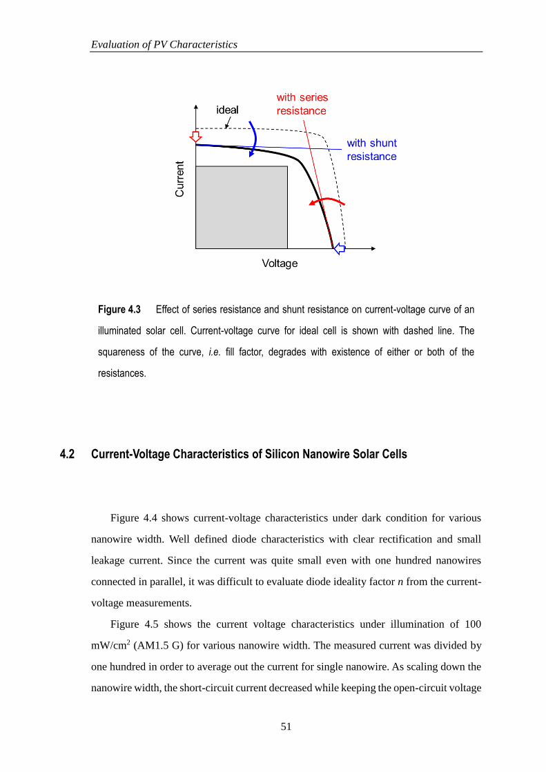
Figure 4.3 shows a schematic illustration for the effect of series resistance and shunt
resistance on current-voltage curve of an illuminated solar cell. Current-voltage curve for
ideal cell is shown with dashed line. The series resistances degrade the current and the
shunt resistance degrade the open-circuit voltage of the cell. Therefore, the existence of
these resistances can be observed by evaluating the fill factor of the cell.
Figure 4.2 Current-voltage curve of an ideal solar cell (Rs = 0, Rsh = ) with Iph = 55 mA, I01
= 10-13 A, I02 = 10-13 A, n1 = 1, n2 = 2, T = 300 K. The maximum power point and schematic
expression of the fill factor (FF) are shown in the figure.
Evaluation of PV Characteristics
51
4.2 Current-Voltage Characteristics of Silicon Nanowire Solar Cells
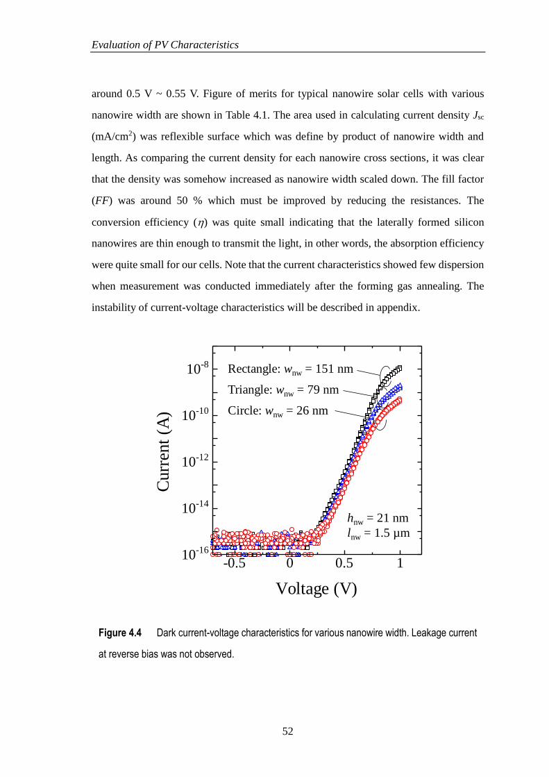
Figure 4.4 shows current-voltage characteristics under dark condition for various
nanowire width. Well defined diode characteristics with clear rectification and small
leakage current. Since the current was quite small even with one hundred nanowires
connected in parallel, it was difficult to evaluate diode ideality factor n from the current-
voltage measurements.
Figure 4.5 shows the current voltage characteristics under illumination of 100
mW/cm2 (AM1.5 G) for various nanowire width. The measured current was divided by
one hundred in order to average out the current for single nanowire. As scaling down the
nanowire width, the short-circuit current decreased while keeping the open-circuit voltage
Figure 4.3 Effect of series resistance and shunt resistance on current-voltage curve of an
illuminated solar cell. Current-voltage curve for ideal cell is shown with dashed line. The
squareness of the curve, i.e. fill factor, degrades with existence of either or both of the
resistances.
Evaluation of PV Characteristics
52
around 0.5 V ~ 0.55 V. Figure of merits for typical nanowire solar cells with various
nanowire width are shown in Table 4.1. The area used in calculating current density Jsc
(mA/cm2) was reflexible surface which was define by product of nanowire width and
length. As comparing the current density for each nanowire cross sections, it was clear
that the density was somehow increased as nanowire width scaled down. The fill factor
(FF) was around 50 % which must be improved by reducing the resistances. The
conversion efficiency () was quite small indicating that the laterally formed silicon
nanowires are thin enough to transmit the light, in other words, the absorption efficiency
were quite small for our cells. Note that the current characteristics showed few dispersion
when measurement was conducted immediately after the forming gas annealing. The
instability of current-voltage characteristics will be described in appendix.
Figure 4.4 Dark current-voltage characteristics for various nanowire width. Leakage current
at reverse bias was not observed.
Curr
ent
(A)
Voltage (V)
hnw = 21 nm
lnw = 1.5 µm
Triangle: wnw = 79 nm
Circle: wnw = 26 nm
Rectangle: wnw = 151 nm
10.50-0.510-16
10-14
10-12
10-10
10-8

Evaluation of PV Characteristics
53
Figure 4.5 Current-voltage characteristics under illumination of 100 mW/cm2 (AM1.5 G) for
various nanowire width. Current decreased as nanowire width scaled down. The open-
circuit voltage was around 0.5 V. Data shown in the figure are the average of 100 nanowires
connected in parallel.
Table 4.1 Figure of merits for typical nanowire solar cells

Evaluation of PV Characteristics
54
4.3 Effects of Interface States on PV Characteristics
4.3.1 Effects of Nanowire Narrowing
Figure 4.6 shows a summary of short-circuit current and open-circuit voltage against
nanowire width for two different nanowire length lnw = 1.5, 9 m. The short-circuit
current decreased as nanowire width scaled down while the open-circuit kept the same or
showed no clear dependence on nanowire width. When comparing these two different
nanowire length, as shown in the figure, the slope of short circuit-current clearly changed
at wnw ~ 75 nm in short nanowires (lnw = 1.5 m) while proportionally decreased in long
nanowires (lnw = 9 m). For open-circuit voltage, there were no clear dependence on
nanowire width was observed.
4.3.2 Effects of Surface Recombination at Depletion Region
Figure 4.7 shows the short-circuit current and open-circuit voltage against undoped
depletion region length with various nanowire width. The short-circuit current showed
different peaks for each width. This peak shift to shorter length as the nanowire width
scaled down. Figure 4.8 shows a summary of peak position.

Evaluation of PV Characteristics
55
(a)
(b)
Figure 4.6 Effect of nanowire width (wnw) scaling on solar cell (a) short-circuit current Isc and
(b) open-circuit voltage Voc for various nanowire length. Isc first gradually decreased as wnw
scaled down, and abruptly degrade under ~ 80 nm. However, Isc slightly increased for nanowires
with wnw < 50 nm. Voc varied around 0.50 ~ 0.55 V which showed no clear dependence on wnw.
Nanowire width wnw (nm)
Sh
ort
-cir
cuit
curr
ent
I sc (
pA
)
hnw = 21 nm
lnw = 1.5 µm
Under 100 mW/cm2 (AM1.5 G)
Rectangle: lnw = 9 µm
Circle: lnw = 1.5 µm
0 50 100 150
1
2
3
4
Nanowire width wnw (nm)
Op
en-c
ircu
it v
olt
age
Vo
c (
V) hnw = 21 nm
Rectangle: lnw = 9.0 µm
Triangle: lnw = 3.5 µm
Circle: lnw = 1.5 µm
Under 100 mW/cm2 (AM1.5 G)
0 50 100 150
0.4
0.5
0.6
0.7

Evaluation of PV Characteristics
56
(a)
(b)
Figure 4.7 Effect of undoped region length (lnw) on solar cell (a) short-circuit current Isc and
(b) open-circuit voltage Voc. The peak shifts of Isc is indicating higher surface recombination in
smaller nanowires limit the collection of generated carriers in undoped region. Voc varied around
0.50 ~ 0.55 V which showed no clear dependence on lnw.
Sh
ort
-cir
cuit
curr
ent
I sc (
pA
) Under 100 mW/cm2 (AM1.5 G)
hnw = 21 nmwnw = 150 nm
wnw = 79 nm
wnw = 56 nm
wnw = 26 nm
Undoped region length lnw (µm)
0 2 4 6 8 10
2
4
6
Op
en-c
ircu
it v
olt
age
Vo
c (
V) Under 100 mW/cm2 (AM1.5 G)
hnw = 21 nm
Rectangle: wnw = 150 nm
Triangle: wnw = 79 nm
Rev. Triangle: wnw = 56 nm
Circle: wnw = 23 nm
Undoped region length lnw (µm)
0 2 4 6 8 10
0.4
0.5
0.6
0.7
Evaluation of PV Characteristics
57
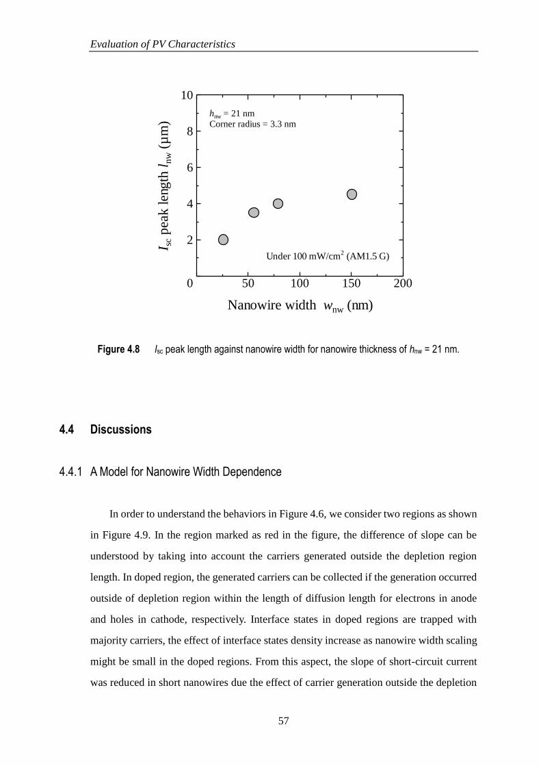
4.4 Discussions
4.4.1 A Model for Nanowire Width Dependence
In order to understand the behaviors in Figure 4.6, we consider two regions as shown
in Figure 4.9. In the region marked as red in the figure, the difference of slope can be
understood by taking into account the carriers generated outside the depletion region
length. In doped region, the generated carriers can be collected if the generation occurred
outside of depletion region within the length of diffusion length for electrons in anode
and holes in cathode, respectively. Interface states in doped regions are trapped with
majority carriers, the effect of interface states density increase as nanowire width scaling
might be small in the doped regions. From this aspect, the slope of short-circuit current
was reduced in short nanowires due the effect of carrier generation outside the depletion
Figure 4.8 Isc peak length against nanowire width for nanowire thickness of hnw = 21 nm.
Nanowire width wnw (nm)
I sc p
eak
len
gth
ln
w (
µm
)
Under 100 mW/cm2 (AM1.5 G)
hnw = 21 nm
Corner radius = 3.3 nm
0 50 100 150 200
2
4
6
8
10

Evaluation of PV Characteristics
58
region is stronger than the longer nanowires. In the region marked as blue in the figure,
where the slope changed in short nanowires, the effect of sidewalls and corners will
abruptly increase. Since the density of interface states are quite high at sidewalls and
corners, as described in chapter 3, the effects on surface recombination might be more
obvious in small nanowire width. The slight increase of current in smaller width can be
understood by including the effect of optimum length that the smaller nanowires are
approaching the optimum length as discuss in next section.
4.4.2 A Model for Nanowire Length Dependence
Figure 4.10 shows schematic illustration of a model for depletion region length
dependence. Depletion region length are shown as red square. We consider average length
Figure 4.9 Explanations for Isc – wnw dependence for nanowires with hnw = 21 nm and lnw =
1.5 m. Degradation of Isc as scaling the wnw indicate increasing effects of high Dit in small cross
section nanowires.
Nanowire width wnw (nm)
Sh
ort
-cir
cuit
curr
ent
I sc (
pA
)
hnw = 21 nm
lnw = 1.5 µm
Under 100 mW/cm2 (AM1.5 G)
Rectangle: lnw = 9 µm
Circle: lnw = 1.5 µm
0 50 100 150
1
2
3
4
Increasing effects of recombination
at corners and sidewalls
Effects of carriers generated outside
the undoped region must be considered

Evaluation of PV Characteristics
59
(LD) that generated carriers can drift inside the depletion region. When the carriers
generated in the depletion region, they are immediately drift to opposite side due to the
electric field inside the depletion region. Since interface states at the depletion are active
as recombination centers and can trap or detrap carriers drifting the depletion regions, the
length of carriers can drift are limited by the surface recombination. At the peak position
of the short-circuit current, the length of depletion region and LD matches. In other words,
the depletion region length are sufficient absorb capable light and not exceeding the
length that generated carriers can drift without affected by surface recombination. From
this view point, this length must vary as the density of interface state changes even is the
cross section are same.
Figure 4.10 Schematic illustration of a model for depletion region length dependence of short-
circuit current Isc. The peak observed in the measured data corresponds to figure B where the
depletion region length matches the drift length of generated carriers.
Length lnw
Short
-circuit c
urr
ent I
sc
Optimum length
Lopt
A
B
C
A: lnw < Lopt
B: lnw = Lopt
C: lnw > Lopt
Depletion region lnw
n p
eEte hEth
n p
n p
Recombination
at Dit

Evaluation of PV Characteristics
60
4.5 Conclusions for This Chapter
In this chapter, the photovoltaic characteristics of nanowire solar cells with various
nanowire cross section and length. The effects of surface recombination on current-
voltage characteristics are investigated by comparing data from nanowires with different
sizes. The effects of surface recombination at the interface states strongly affects the solar
cell performance especially in smaller nanowires. Taking into account the slight increase
in short-circuit current in small width, further improvement might be achieved by
optimizing the nanowire surface passivation. Also from the measurement of current-
voltage characteristics of different nanowire length, the existence of optimum nanowire
length was observed.
Evaluation of PV Characteristics
61
References
[4.1] A. Luque and S. Hegedus, Handbook of Photovoltaic Science and Engineering,
Second Edition, 2011.
Effects of Surface Properties
5 Effects of Surface Properties
In this chapter, the effects of surface potential fluctuation on PV characteristics of
silicon nanowire solar cells are experimentally discuss by adopted backgated diode
structures. The method is based on the principles of surface effects on gated diodes [5.1].
By applying voltage to the substrates, the bottom surface potential of silicon nanowire
solar cells were controlled and the photovoltaic characteristics were measured under
different surface conditions. The control of surface potential was also obtained by
depositing thin Al2O3 layer to the surface of silicon nanowires. The results from gated
solar cells and Al2O3 deposited solar cells were compared.
5.1 Bottom Surface Potential Control
Figure 5.1 shows the evaluation method for effects of surface potential controlling
on solar cells. Substrate electrode formed on back substrate was biased under
illumination, and measured the current-voltage characteristics while applying the
substrate voltage (Vsub). Since the doped region are highly doped and stuck to their
original positions, only the undoped region shifts up or down under negative or positive
bias.
Figure 5.2 shows the illuminated current-voltage characteristics under negative
substrate bias (Vsub) varying from 0 V to −3 V with −0.1 V/step. Short-circuit current
was enhanced at small negative bias around Vsub ~ 0.3 V, however, a kink like
characteristic was observed which degrades the fill factor. The origin of this kink like
62

Effects of Surface Properties
behavior will be discussed later. On the other hand, open-circuit voltage slightly
increased till saturate around 560 mV.
Figure 5.3 shows illuminated current-voltage characteristics under positive
substrate bias (Vsub) varying from 0 V to 3 V with +0.1 V/step. Current abruptly
decreased while the open-circuit voltage first slightly increased and decreased as
applying larger voltage. Short-circuit current and open-circuit current under against
substrate bias are summarized in Figure 5.4.
(a) (b)
Figure 5.1 Evaluation method for effect of surface potential control on photovoltaic
characteristics using substrate bias. (a) Bottom surface potential of silicon nanowire solar cells
shifts as the substrate bias applied. (b) Changes of band diagram in the nanowire under
substrate bias.
p-Si substrate
BOX layern+ p+
Substrate Bias: Vsub
Solar simulator(AM1.5 G, 100 mW/cm2)
GND Vanode
p+n+
Negative Bias
Positive Bias
63
Effects of Surface Properties
Figure 5.2 Illuminated current-voltage characteristics under negative substrate bias (Vsub)
varying from 0 V to −3 V with −0.1 V/step. Short-circuit current was enhanced at small
negative bias around Vsub ~ 0.3 V, however, a kink like characteristic was observed which
degrades the fill factor. Open-circuit voltage slightly increased till saturate around 560 mV.
64

Effects of Surface Properties
Figure 5.3 Illuminated current-voltage characteristics under positive substrate bias (Vsub)
varying from 0 V to 3 V with +0.1 V/step. Current abruptly decreased while the open-circuit
voltage slightly increased.
65

Effects of Surface Properties
(a)
(b)
Figure 5.4 Summary of changes in short-circuit current and open-circuit voltage of a silicon
nanowire solar cell under substrate bias varying from −3 V to 3 V. Negative biased, i.e.
positive shifted surface potential, might be an effective approach to improve the
current-voltage characteristics.
Shor
t-circ
uit c
urre
nt (p
A)
Substrate bias Vsub (V)
Under 100 mW/cm2 (AM1.5 G)
hnw = 42 nmlnw = 1.5 µm
-3 -2 -1 0 1 2 30
0.5
1
1.5
2Negative PositiveO
pen-
circ
uit v
olta
ge (V
)
Substrate bias Vsub (V)
Under 100 mW/cm2 (AM1.5 G)
hnw = 42 nmlnw = 1.5 µm
-3 -2 -1 0 1 2 30.45
0.5
0.55
0.6Negative Positive
66

Effects of Surface Properties
5.2 Demonstration of Surface Potential Control with Thin Al2O3 Layer
Figure 5.5 shows a schematic illustration of surface passivation with thin Al2O3
layer. The Al2O3 layer was deposited by using atomic-layer-deposition (ALD) method
with varying the thickness from 1 nm to 2.5 nm. The Al2O3 layer contains a large
amount of negatively charged defects (fixed charges). This fixed charges induce
field-effects at surface of silicon nanowires just like the surface potential control with
negative substrate bias as shown in Figure 5.2. Figure 5.6 shows an example of changes
in current-voltage characteristics under deposition of thin Al2O3 layer on the suface of
silicon nanowires. Short-circuit current decreased abruptly to the alf value of
non-passivated conditions while the open-circuit slightly increased. Figure 5.7 shows a
summary of changes in short-circuit current.
Figure 5.5 Schematic illustration of surface passivation with thin Al2O3 layer using
atomic-layer-deposition method. Al2O3 layer contains negative fixed charges which enable
surface potential shift to the negative as explained in Figure 5.2.
p-Si substrate
BOX layern+ p+
Solar simulator(AM1.5 G, 100 mW/cm2)
GND Vanode
67

Effects of Surface Properties
Figure 5.6 Changes in current-voltage characteristics under deposition of thin Al2O3 layer
on the surface of silicon nanowires. The short-circuit current decreased abruptly while the
open-circuit voltage slightly increased.
Under 100 mW/cm2 (AM1.5 G)
hnw = 21 nmwnw = 56 nmlnw = 1.5 µm
Al2O3 thicknessRectangle: 0 nm
Curr
ent (
pA)
Voltage (V)
Triangle (blue): 1 nm
Circle (red): 2.5 nm
0.60.40.20
0.4
0.8
1.2
68
Effects of Surface Properties
5.3 Discussions
5.3.1 Effects of Bottom Surface Potential Control on PV Characteristics
Figure 5.8 shows schematic illustration of a model for current-voltage
characteristics at short-circuit condition under negative substrate bias. As described
previously, the negative bias shifts the conduction band and valence band of undoped
region. As a result, the electric field of longitudinal direction in the depletion region
enhance for small bias, and showed showed the peak short-circuit current. However,
when applying larger negative bias to the substrate, both the conduction and valence
band keep shifting upward and hole trapping inside the depletion region occur once the
Figure 5.7 A summary of change in short-circuit current under deposition of thin Al2O3
layer on the surface of silicon nanowires.
Shor
t-circ
uit c
urre
nt (p
A)
Substrate bias Vsub (V)
Under 100 mW/cm2 (AM1.5 G)
hnw = 42 nmlnw = 1.5 µm
-3 -2 -1 0 1 2 30
0.5
1
1.5
2
0 nm
1 nm
2.5 nm
69
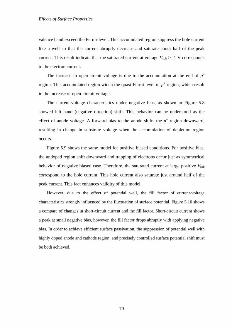
Effects of Surface Properties
valence band exceed the Fermi-level. This accumulated region suppress the hole current
like a well so that the current abruptly decrease and saturate about half of the peak
current. This result indicate that the saturated current at voltage Vsub > -1 V corresponds
to the electron current.
The increase in open-circuit voltage is due to the accumulation at the end of p+
region. This accumulated region widen the quasi-Fermi level of p+ region, which result
in the increase of open-circuit voltage.
The current-voltage characteristics under negative bias, as shown in Figure 5.8
showed left hand (negative direction) shift. This behavior can be understood as the
effect of anode voltage. A forward bias to the anode shifts the p+ region downward,
resulting in change in substrate voltage when the accumulation of depletion region
occurs.
Figure 5.9 shows the same model for positive biased conditions. For positive bias,
the undoped region shift downward and trapping of electrons occur just as symmetrical
behavior of negative biased case. Therefore, the saturated current at large positive Vsub
correspond to the hole current. This hole current also saturate just around half of the
peak current. This fact enhances validity of this model.
However, due to the effect of potential well, the fill factor of current-voltage
characteristics strongly influenced by the fluctuation of surface potential. Figure 5.10 shows
a compare of changes in short-circuit current and the fill factor. Short-circuit current shows
a peak at small negative bias, however, the fill factor drops abruptly with applying negative
bias. In order to achieve efficient surface passivation, the suppression of potential well with
highly doped anode and cathode region, and precisely controlled surface potential shift must
be both achieved.
70
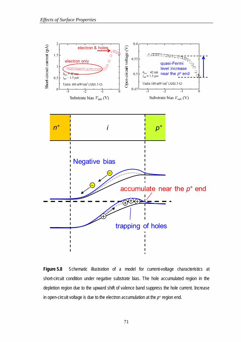
Effects of Surface Properties
Figure 5.8 Schematic illustration of a model for current-voltage characteristics at
short-circuit condition under negative substrate bias. The hole accumulated region in the
depletion region due to the upward shift of valence band suppress the hole current. Increase
in open-circuit voltage is due to the electron accumulation at the p+ region end.
71
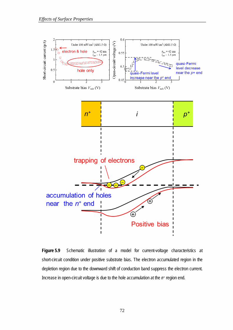
Effects of Surface Properties
Figure 5.9 Schematic illustration of a model for current-voltage characteristics at
short-circuit condition under positive substrate bias. The electron accumulated region in the
depletion region due to the downward shift of conduction band suppress the electron current.
Increase in open-circuit voltage is due to the hole accumulation at the n+ region end.
72
Effects of Surface Properties
5.3.2 Effects of Surface Passivation with Thin Al2O3 Layer
Figure 5.11 concludes the effect of surface passivation with thin Al2O3 layer used in
this work. As shown in the figure, the thermal oxide layer contains positive charges and
the Al2O3 layer contains negative charges which shifts the surface potential negative and
positive, respectively. The optimum shifts in surface potential must be achieved by
controlling the amount of total fixed charges by taking the balanced thicknesses
between different materials with reverse polarity.
Figure 5.10 Short-circuit current and fill factor against substrate bias (Vsub). Our nanowire
solar cells shows a peak short-circuit current at Vsub ~ 0.3 V, however, the fill factor is
minimum at the voltage due to the kink shaped current-voltage characteristics.
Shor
t-circ
uit c
urre
n t (p
A)
Substrate bias Vsub (V)
Under 100 mW/cm2 (AM1.5 G)
hnw = 42 nmlnw = 1.5 µm
Fill
fact
or (%
)
-3 -2 -1 0 1 2 30
0.5
1
1.5
2
0
20
40
60
80
100
73
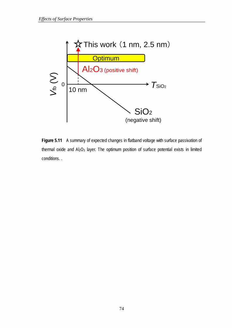
Effects of Surface Properties
Figure 5.11 A summary of expected changes in flatband voltage with surface passivation of
thermal oxide and Al2O3 layer. The optimum position of surface potential exists in limited
conditions. .
Al2O3 (positive shift)
OptimumV
fb(V
)
TSiO2
SiO2(negative shift)
0
This work (1 nm, 2.5 nm)
10 nm
74
Effects of Surface Properties
5.4 Conclusions for This Chapter
In this chapter, the effects of surface potential control on silicon nanowire solar cell
was discussed. From the measurement using substrate bias, the sensitiveness of silicon
nanowire solar cells to the change of surface potential are proved to be extreme. The
current-voltage characteristics of nanowire solar cells can be modulated by controlling
the surface potential, however, there are quite small window for optimize the
performance with surface passivation. In order to enhance the performance, precise
control of surface potential and position of the nanowires are necessary.
75

Effects of Surface Properties
References
[5.1] A. S. Groove and D. J. Fitzgerald, “Surface Effects on p-n Junctions:
Characteristics of Surface Space-Charge Region Under Non-Equilibrium
Conditions,” Solid-State Eletron., vol. 9, pp. 783-806, 1966.
76
Conclusions
77
6 Conclusions
In this thesis, the effects of interface states on silicon nanowire solar cells and
importance of surface potential controlling for enhancement of solar cell performance
are experimentally studied and proved.
From the measurement of interface states density by adopting charge pumping
method to gated silicon nanowire diodes, extremely high density of interface states exist
at the rounded corners of silicon nanowires. The instability of hydrogen termination of
rounded corners were also examined by adopting electrical stress to the thermal oxide
interface with gated diodes followed by charge pumping measurement. From this view
point, management and prevent of the surface rounding is necessary for reduction of
interface states, i.e. surface recombination, and improvement of efficiency of silicon
nanowire solar cells.
The effects of interface states on silicon nanowire solar cells are experimentally
investigated by changing the nanowire cross-section and length. From the measurement
with different cross-section nanowires, the effect of high interface state density at
sidewalls and rounded corners on solar cell performance will be obvious in small
nanowires. Also it was shown that the interface states affect the optimum depletion
region length of p-i-n solar cell structures. The optimizing of depletion region length
strongly depends on interface state density at surface passivation interfaces.
In order to suppress the effect of interface states on solar cell performances, we
proposed surface potential controlling based surface passivation technique. From the
experiment of current measurement under bottom surface potential controlling with
substrate bias, the sensitiveness of nanowire solar cells to the surface potential was
Conclusions
78
clearly observed. Since the surface passivation of nanowire solar cell must take into
account both n+ region and p+ region, the optimized surface potential for each of the
position of the nanowires exists for the improvement of efficiency.

Presentations
Presentations
International Conference (first author)
[1] T. Shoji, K. Kakushima, Y. Kataoka, A. Nishiyama, N. Sugii, H. Wakabayashi, K.
Tsutsui, K. Natori, H. Iwai, “Effect of Surface Potential Control and Interface States
for Silicon Nanowire Solar Cells,” European PV Solar Energy Conference and
Exhibition, Sep, 2014, Amsterdam, the Netherlands.
Domestic Conferences (first author)
[1] T. Shoji, K. Ishikawa, K. Kakushima, Y. Kataoka, A. Nishiyama, N. Sugii, H.
Wakabayashi, K. Tsutsui, K. Natori, H. Iwai, “Identification of Trap Sites at
Dielectric/Three-Dimensional Si Structure Interfaces,” The 74th Japan Society of
Applied Physics Autumn Meeting, Sep. 2013, Kyoto, Japan.
[2] T. Shoji, K. Kakushima, Y. Kataoka, A. Nishiyama, N. Sugii, H. Wakabayashi, K.
Tsutsui, K. Natori, H. Iwai, “A Study on Interface State Density at Si Nanowire and
SiO2 Interfaces,” The 61st Japan Society of Applied Physics Spring Meeting, Mar.
2014, Sagamihara, Japan.
79

Acknowledgements
Acknowledgements
I would like to express my deep gratitude first and foremost to Prof.
Hiroshi Iwai of Tokyo Institute of Technology for his consistent, always kind
and to the point guidance as my adviser on this thesis.
I am also grateful to A. Prof. Kuniyuki Kakushima, Prof. Kazuo Tsusui,
Prof. Hitoshi Wakabayashi, Prof. Yoshinori Kataoka, Prof. Akira Nishiyama,
Prof. Nobuyuki Sugii, and Prof. Kenji Natori, for their invaluable guidance
and help throughout my research.
I truly appreciate all the colleagues in Prof. Iwai’s laboratory, for fruitful
discussions, kind hospitality and friendships. I am also grateful to Dr. Yan
Wu and Dr. Dariush Hassan Zadeh for their assistance with the experiments
and invaluable advices on my research.
I would also like to thank Prof. Iwai’s secretaries Ms. Akiko Matsumoto
and Masako Nishizawa for their kind support and help with filling and
handling in numerous and various documents throughout my days in master
student years.
Finally, I would like to express my deepest gratitude to my family Naoki,
Naoko, and Takuya for their continuous and unconditional support,
encouragement, and help, as I am indebted all my accomplishments to them.
80