Embed Size (px)
DESCRIPTION
flip flops
Citation preview
624 IEEE TRANSACTIONS ON VERY LARGE SCALE INTEGRATION (VLSI) SYSTEMS, VOL. 21, NO. 4, APRIL 2013
Effective and Efficient Approach for PowerReduction by Using Multi-Bit Flip-Flops
Ya-Ting Shyu, Jai-Ming Lin, Chun-Po Huang, Cheng-Wu Lin, Ying-Zu Lin, and Soon-Jyh Chang, Member, IEEE
Abstract— Power has become a burning issue in modern VLSIdesign. In modern integrated circuits, the power consumed byclocking gradually takes a dominant part. Given a design, wecan reduce its power consumption by replacing some flip-flopswith fewer multi-bit flip-flops. However, this procedure mayaffect the performance of the original circuit. Hence, the flip-flopreplacement without timing and placement capacity constraintsviolation becomes a quite complex problem. To deal with thedifficulty efficiently, we have proposed several techniques. First,we perform a co-ordinate transformation to identify those flip-flops that can be merged and their legal regions. Besides, weshow how to build a combination table to enumerate possiblecombinations of flip-flops provided by a library. Finally, we usea hierarchical way to merge flip-flops. Besides power reduction,the objective of minimizing the total wirelength is also considered.The time complexity of our algorithm is �(n1.12) less than theempirical complexity of �(n2). According to the experimentalresults, our algorithm significantly reduces clock power by20–30% and the running time is very short. In the largest testcase, which contains 1 700 000 flip-flops, our algorithm only takesabout 5 min to replace flip-flops and the power reduction canachieve 21%.
Index Terms— Clock power reduction, merging, multi-bitflip-flop, replacement, wirelength.
I. INTRODUCTION
DUE to the popularity of portable electronic products,low power system has attracted more attention in recent
years. As technology advances, an systems-on-a-chip (SoC)design can contain more and more components that lead toa higher power density. This makes power dissipation reachthe limits of what packaging, cooling or other infrastruc-ture can support. Reducing the power consumption not onlycan enhance battery life but also can avoid the overheatingproblem, which would increase the difficulty of packagingor cooling [1], [2]. Therefore, the consideration of powerconsumption in complex SOCs has become a big challengeto designers. Moreover, in modern VLSI designs, powerconsumed by clocking has taken a major part of the wholedesign especially for those designs using deeply scaled CMOStechnologies [3]. Thus, several methodologies [4], [5] havebeen proposed to reduce the power consumption of clocking.
Manuscript received February 1, 2011; revised August 22, 2011; acceptedFebruary 16, 2012. Date of publication April 5, 2012; date of current versionMarch 18, 2013. This work was supported in part by the National ScienceCouncil of Taiwan under Grant 100-2220-E-006-005.
The authors are with the Department of Electrical Engineering,National Cheng-Kung University, Tainan 70101, Taiwan (e-mail: [email protected]; [email protected]; [email protected];[email protected]; [email protected]; [email protected]).
Color versions of one or more of the figures in this paper are availableonline at http://ieeexplore.ieee.org.
Digital Object Identifier 10.1109/TVLSI.2012.2190535
0.35 0.25 0.18 0.13 0.09024681012141618
Technology(μm)
Load
ingNum
ber
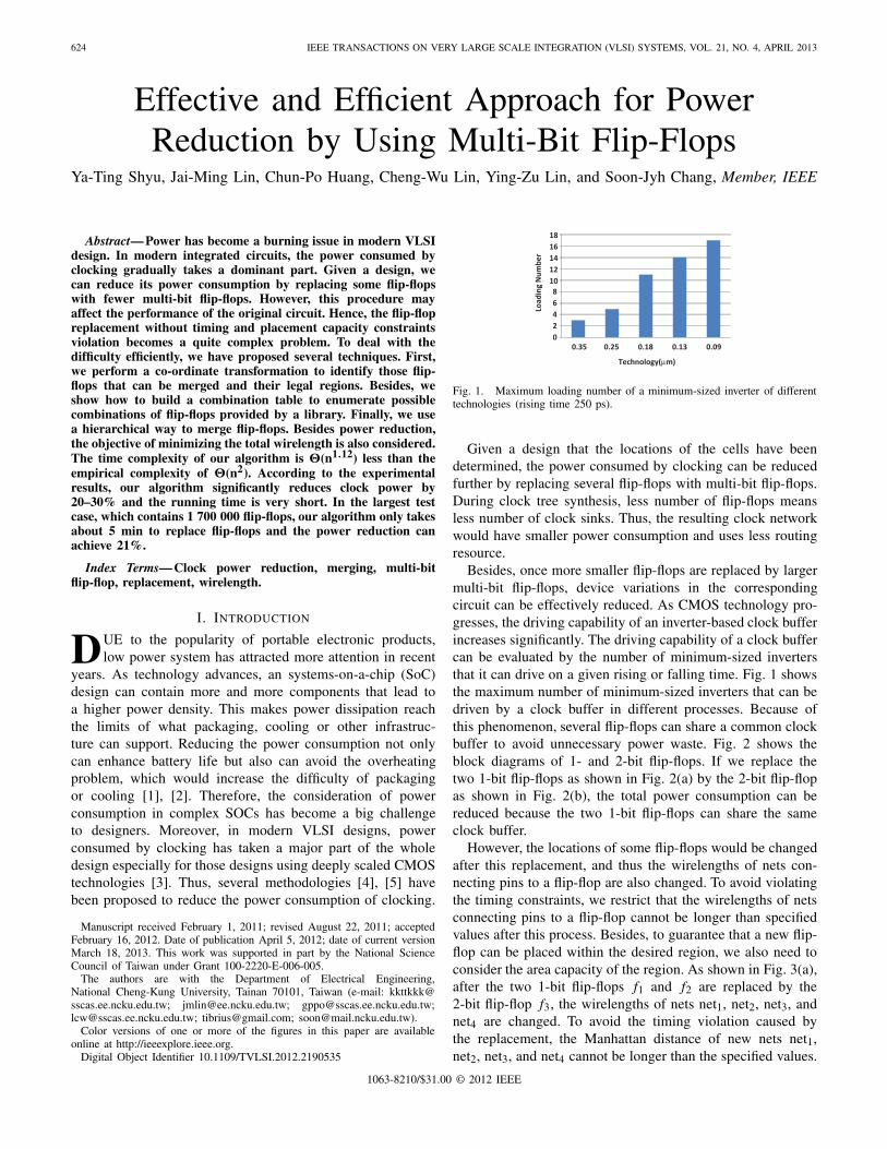
Fig. 1. Maximum loading number of a minimum-sized inverter of differenttechnologies (rising time 250 ps).
Given a design that the locations of the cells have beendetermined, the power consumed by clocking can be reducedfurther by replacing several flip-flops with multi-bit flip-flops.During clock tree synthesis, less number of flip-flops meansless number of clock sinks. Thus, the resulting clock networkwould have smaller power consumption and uses less routingresource.
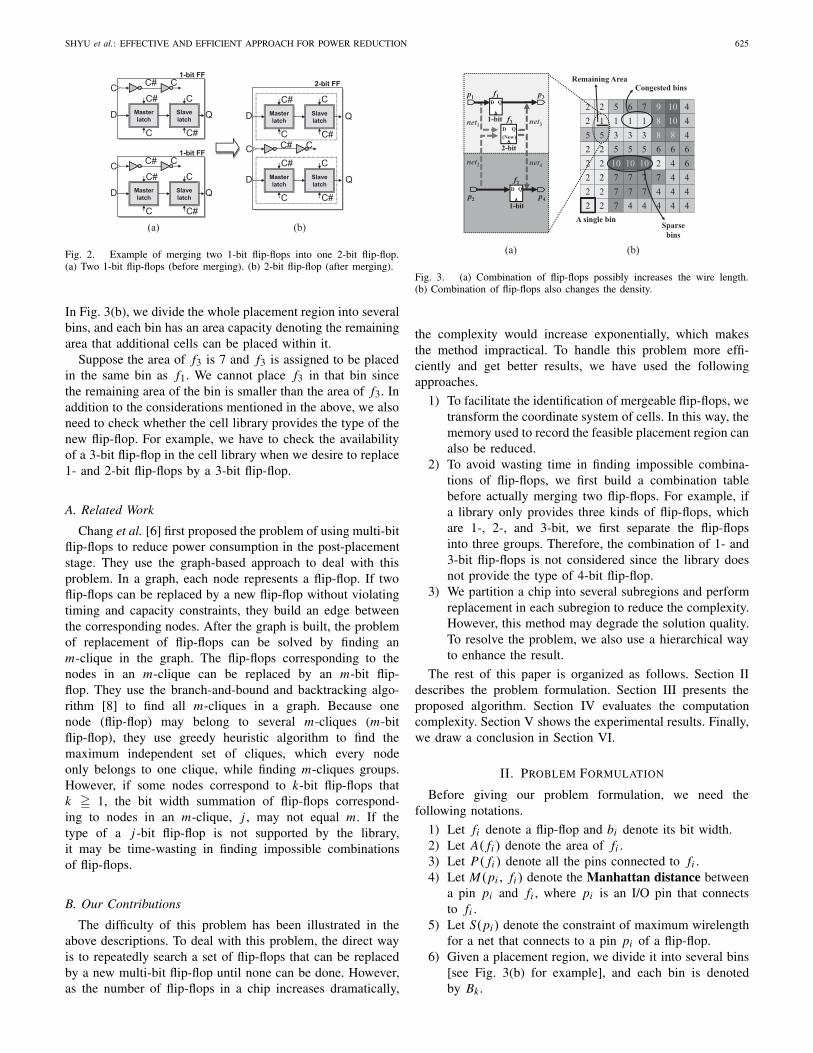
Besides, once more smaller flip-flops are replaced by largermulti-bit flip-flops, device variations in the correspondingcircuit can be effectively reduced. As CMOS technology pro-gresses, the driving capability of an inverter-based clock bufferincreases significantly. The driving capability of a clock buffercan be evaluated by the number of minimum-sized invertersthat it can drive on a given rising or falling time. Fig. 1 showsthe maximum number of minimum-sized inverters that can bedriven by a clock buffer in different processes. Because ofthis phenomenon, several flip-flops can share a common clockbuffer to avoid unnecessary power waste. Fig. 2 shows theblock diagrams of 1- and 2-bit flip-flops. If we replace thetwo 1-bit flip-flops as shown in Fig. 2(a) by the 2-bit flip-flopas shown in Fig. 2(b), the total power consumption can bereduced because the two 1-bit flip-flops can share the sameclock buffer.
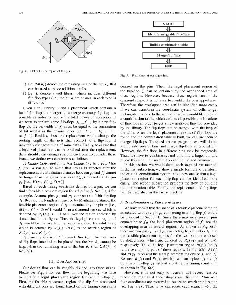
However, the locations of some flip-flops would be changedafter this replacement, and thus the wirelengths of nets con-necting pins to a flip-flop are also changed. To avoid violatingthe timing constraints, we restrict that the wirelengths of netsconnecting pins to a flip-flop cannot be longer than specifiedvalues after this process. Besides, to guarantee that a new flip-flop can be placed within the desired region, we also need toconsider the area capacity of the region. As shown in Fig. 3(a),after the two 1-bit flip-flops f1 and f2 are replaced by the2-bit flip-flop f3, the wirelengths of nets net1, net2, net3, andnet4 are changed. To avoid the timing violation caused bythe replacement, the Manhattan distance of new nets net1,net2, net3, and net4 cannot be longer than the specified values.
1063-8210/$31.00 © 2012 IEEE
SHYU et al.: EFFECTIVE AND EFFICIENT APPROACH FOR POWER REDUCTION 625
Masterlatch
Slavelatch
C
D Q
C# C
C# C
C#C
1-bit FF
Masterlatch
Slavelatch
C
D Q
C# C
C# C
C#C
1-bit FF
Masterlatch
Slavelatch
C
D Q
C# C
C# C
C#C
2-bit FF
Masterlatch
SlavelatchD Q
C# C
C#C
(a) (b)
Fig. 2. Example of merging two 1-bit flip-flops into one 2-bit flip-flop.(a) Two 1-bit flip-flops (before merging). (b) 2-bit flip-flop (after merging).
In Fig. 3(b), we divide the whole placement region into severalbins, and each bin has an area capacity denoting the remainingarea that additional cells can be placed within it.
Suppose the area of f3 is 7 and f3 is assigned to be placedin the same bin as f1. We cannot place f3 in that bin sincethe remaining area of the bin is smaller than the area of f3. Inaddition to the considerations mentioned in the above, we alsoneed to check whether the cell library provides the type of thenew flip-flop. For example, we have to check the availabilityof a 3-bit flip-flop in the cell library when we desire to replace1- and 2-bit flip-flops by a 3-bit flip-flop.
A. Related Work
Chang et al. [6] first proposed the problem of using multi-bitflip-flops to reduce power consumption in the post-placementstage. They use the graph-based approach to deal with thisproblem. In a graph, each node represents a flip-flop. If twoflip-flops can be replaced by a new flip-flop without violatingtiming and capacity constraints, they build an edge betweenthe corresponding nodes. After the graph is built, the problemof replacement of flip-flops can be solved by finding anm-clique in the graph. The flip-flops corresponding to thenodes in an m-clique can be replaced by an m-bit flip-flop. They use the branch-and-bound and backtracking algo-rithm [8] to find all m-cliques in a graph. Because onenode (flip-flop) may belong to several m-cliques (m-bitflip-flop), they use greedy heuristic algorithm to find themaximum independent set of cliques, which every nodeonly belongs to one clique, while finding m-cliques groups.However, if some nodes correspond to k-bit flip-flops thatk � 1, the bit width summation of flip-flops correspond-ing to nodes in an m-clique, j , may not equal m. If thetype of a j -bit flip-flop is not supported by the library,it may be time-wasting in finding impossible combinationsof flip-flops.
B. Our Contributions
The difficulty of this problem has been illustrated in theabove descriptions. To deal with this problem, the direct wayis to repeatedly search a set of flip-flops that can be replacedby a new multi-bit flip-flop until none can be done. However,as the number of flip-flops in a chip increases dramatically,
2 2 5 6 7 9 10 42 1 1 1 1 8 10 45 5 3 3 3 8 8 42 2 5 5 5 6 6 62 2 10 10 10 2 4 62 2 7 7 7 7 4 42 2 7 7 7 4 4 42 2 7 4 4 4 4 4
Congested bins
Sparsebins
p3
2-bit
f1p1
p2
net1
net2
net3
net4
D Q
D Q(New)
1-bit f3
f2D Q
1-bit p4
A single bin
Remaining Area
(a) (b)
Fig. 3. (a) Combination of flip-flops possibly increases the wire length.(b) Combination of flip-flops also changes the density.
the complexity would increase exponentially, which makesthe method impractical. To handle this problem more effi-ciently and get better results, we have used the followingapproaches.
1) To facilitate the identification of mergeable flip-flops, wetransform the coordinate system of cells. In this way, thememory used to record the feasible placement region canalso be reduced.
2) To avoid wasting time in finding impossible combina-tions of flip-flops, we first build a combination tablebefore actually merging two flip-flops. For example, ifa library only provides three kinds of flip-flops, whichare 1-, 2-, and 3-bit, we first separate the flip-flopsinto three groups. Therefore, the combination of 1- and3-bit flip-flops is not considered since the library doesnot provide the type of 4-bit flip-flop.
3) We partition a chip into several subregions and performreplacement in each subregion to reduce the complexity.However, this method may degrade the solution quality.To resolve the problem, we also use a hierarchical wayto enhance the result.
The rest of this paper is organized as follows. Section IIdescribes the problem formulation. Section III presents theproposed algorithm. Section IV evaluates the computationcomplexity. Section V shows the experimental results. Finally,we draw a conclusion in Section VI.
II. PROBLEM FORMULATION
Before giving our problem formulation, we need thefollowing notations.
1) Let fi denote a flip-flop and bi denote its bit width.2) Let A( fi ) denote the area of fi .3) Let P( fi ) denote all the pins connected to fi .4) Let M(pi , fi ) denote the Manhattan distance between
a pin pi and fi , where pi is an I/O pin that connectsto fi .
5) Let S(pi ) denote the constraint of maximum wirelengthfor a net that connects to a pin pi of a flip-flop.
6) Given a placement region, we divide it into several bins[see Fig. 3(b) for example], and each bin is denotedby Bk .
626 IEEE TRANSACTIONS ON VERY LARGE SCALE INTEGRATION (VLSI) SYSTEMS, VOL. 21, NO. 4, APRIL 2013
p1
f1D Q p2
S(p1)S(p2)
Rp(p1) Rp(p2)
R(f1)
Fig. 4. Defined slack region of the pin.
7) Let RA(Bk) denote the remaining area of the bin Bk thatcan be used to place additional cells.
8) Let L denote a cell library which includes differentflip-flop types (i.e., the bit width or area in each type isdifferent).
Given a cell library L and a placement which contains alot of flip-flops, our target is to merge as many flip-flops aspossible in order to reduce the total power consumption. Ifwe want to replace some flip-flops f1,..., f j−1 by a new flip-flop f j , the bit width of f j must be equal to the summationof bit widths in the original ones (i.e., �bi = b j , i = 1to j−1). Besides, since the replacement would change therouting length of the nets that connect to a flip-flop, itinevitably changes timing of some paths. Finally, to ensure thata legalized placement can be obtained after the replacement,there should exist enough space in each bin. To consider theseissues, we define two constraints as follows.
1) Timing Constraint for a Net Connecting to a Flip-Flopf j from a Pin pi : To avoid that timing is affected after thereplacement, the Manhattan distance between pi and f j cannotbe longer than the given constraint S(pi ) defined on the pinpi [i.e., M(pi , f j ) ≤ S(pi )].
Based on each timing constraint defined on a pin, we canfind a feasible placement region for a flip-flop fj . See Fig. 4 forexample. Assume pins p1 and p2 connect to a 1-bit flip-flopf1. Because the length is measured by Manhattan distance, thefeasible placement region of f1 constrained by the pin pi [i.e.,M(pi , f1) ≤ S(pi )] would form a diamond region, which isdenoted by Rp(pi ), i = 1 or 2. See the region enclosed bydotted lines in the figure. Thus, the legal placement region off1 would be the overlapping region enclosed by solid lines,which is denoted by R( f1). R( f1) is the overlap region ofRp(p1) and Rp(p2).
2) Capacity Constraint for Each Bin Bk : The total areaof flip-flops intended to be placed into the bin Bk cannot belarger than the remaining area of the bin Bk (i.e., �A( fi ) ≤RA(Bk)).
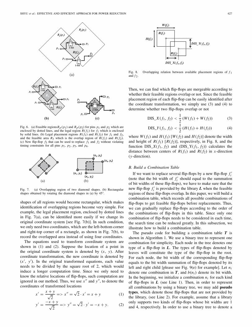
III. OUR ALGORITHM
Our design flow can be roughly divided into three stages.Please see Fig. 5 for our flow. In the beginning, we haveto identify a legal placement region for each flip-flop fi .First, the feasible placement region of a flip-flop associatedwith different pins are found based on the timing constraints
Build a combination table
END
START
Merge flip-flops
Identify mergeable flip-flops
Fig. 5. Flow chart of our algorithm.
defined on the pins. Then, the legal placement region ofthe flip-flop fi can be obtained by the overlapped area ofthese regions. However, because these regions are in thediamond shape, it is not easy to identify the overlapped area.Therefore, the overlapped area can be identified more easilyif we can transform the coordinate system of cells to getrectangular regions. In the second stage, we would like to builda combination table, which defines all possible combinationsof flip-flops in order to get a new multi-bit flip-flop providedby the library. The flip-flops can be merged with the help ofthe table. After the legal placement regions of flip-flops arefound and the combination table is built, we can use them tomerge flip-flops. To speed up our program, we will dividea chip into several bins and merge flip-flops in a local bin.However, the flip-flops in different bins may be mergeable.Thus, we have to combine several bins into a larger bin andrepeat this step until no flip-flop can be merged anymore.
In this section, we would detail each stage of our method.In the first subsection, we show a simple formula to transformthe original coordination system into a new one so that a legalplacement region for each flip-flop can be identified moreeasily. The second subsection presents the flow of buildingthe combination table. Finally, the replacements of flip-flopswill be described in the last subsection.
A. Transformation of Placement Space
We have shown that the shape of a feasible placement regionassociated with one pin pi connecting to a flip-flop fi wouldbe diamond in Section II. Since there may exist several pinsconnecting to f i , the legal placement region of f i are theoverlapping area of several regions. As shown in Fig. 6(a),there are two pins p1 and p2 connecting to a flip-flop f1, andthe feasible placement regions for the two pins are enclosedby dotted lines, which are denoted by Rp(p1) and Rp(p2),respectively. Thus, the legal placement region R( f1) for f1is the overlapping part of these regions. In Fig. 6(b), R( f1)and R( f2) represent the legal placement regions of f1 and f2.Because R( f1) and R( f2) overlap, we can replace f1 and f2by a new flip-flop f3 without violating the timing constraint,as shown in Fig. 6(c).
However, it is not easy to identify and record feasibleplacement regions if their shapes are diamond. Moreover,four coordinates are required to record an overlapping region[see Fig. 7(a)]. Thus, if we can rotate each segment 45°, the
SHYU et al.: EFFECTIVE AND EFFICIENT APPROACH FOR POWER REDUCTION 627
p1
f1D Q
1-bit
p2
p3f2
D
1-bit
p4
Q
R(f1)
Rp(p1)
Rp(p2)
(a)
p1
f1D Q
1-bit
p2
p3f2
D
1-bit
p4
R(f1)
R(f2)
R3
Q
p4
p1
p2
p3
f3D Q
2-bit
(b) (c)
Fig. 6. (a) Feasible regionsRp (p1) and Rp(p2) for pins p1 and p2 which areenclosed by dotted lines, and the legal region R( f1) for f1 which is enclosedby solid lines. (b) Legal placement regions R( f1) and R( f2) for f1 and f2,and the feasible area R3 which is the overlap region of R( f1) and R( f2).(c) New flip-flop f3 that can be used to replace f1 and f2 without violatingtiming constraints for all pins p1, p2, p3, and p4.
(x1, y1)
(x2, y2)
(x3, y3)
(x4, y4)
(a) (b)
Fig. 7. (a) Overlapping region of two diamond shapes. (b) Rectangularshapes obtained by rotating the diamond shapes in (a) by 45°.
shapes of all regions would become rectangular, which makesidentification of overlapping regions become very simple. Forexample, the legal placement region, enclosed by dotted linesin Fig. 7(a), can be identified more easily if we change itsoriginal coordinate system [see Fig. 7(b)]. In such condition,we only need two coordinates, which are the left-bottom cornerand right-top corner of a rectangle, as shown in Fig. 7(b), torecord the overlapped area instead of using four coordinates.
The equations used to transform coordinate system areshown in (1) and (2). Suppose the location of a point inthe original coordinate system is denoted by (x , y). Aftercoordinate transformation, the new coordinate is denoted by(x ′, y ′). In the original transformed equations, each valueneeds to be divided by the square root of 2, which wouldinduce a longer computation time. Since we only need toknow the relative locations of flip-flops, such computation areignored in our method. Thus, we use x ′′ and y ′′, to denote thecoordinates of transformed locations
x ′ = x + y√2
=> x ′′ = √2 · x ′ = x + y (1)
y ′ = −x + y√2
=> y ′′ = √2 · y ′ = −x + y. (2)
R(f1)
R(f2)
DIS_X( f1, f2)
DIS_Y( f1, f2)H(f1)
W(f1)
Fig. 8. Overlapping relation between available placement regions of f 1and f 2.
Then, we can find which flip-flops are mergeable according towhether their feasible regions overlap or not. Since the feasibleplacement region of each flip-flop can be easily identified afterthe coordinate transformation, we simply use (3) and (4) todetermine whether two flip-flops overlap or not
DIS_X ( f1, f2) <1
2(W ( f1) + W ( f2)) (3)
DIS_Y ( f1, f2) <1
2(H ( f1) + H ( f2)) (4)
where W ( f1) and H ( f1) [W ( f2) and H ( f2)] denote the widthand height of R( f1) [R( f2)], respectively, in Fig. 8, and thefunction DIS_X( f1, f2) and (DIS_Y( f1, f2)) calculates thedistance between centers of R( f1) and R( f2) in x-direction(y-direction).
B. Build a Combination Table
If we want to replace several flip-flops by a new flip-flop f ′i
(note that the bit width of f ′i should equal to the summation
of bit widths of these flip-flops), we have to make sure that thenew flip-flop f ′
i is provided by the library L when the feasibleregions of these flip-flops overlap. In this paper, we will build acombination table, which records all possible combinations offlip-flops to get feasible flip-flops before replacements. Thus,we can gradually replace flip-flops according to the order ofthe combinations of flip-flops in this table. Since only onecombination of flip-flops needs to be considered in each time,the search time can be reduced greatly. In this subsection, weillustrate how to build a combination table.
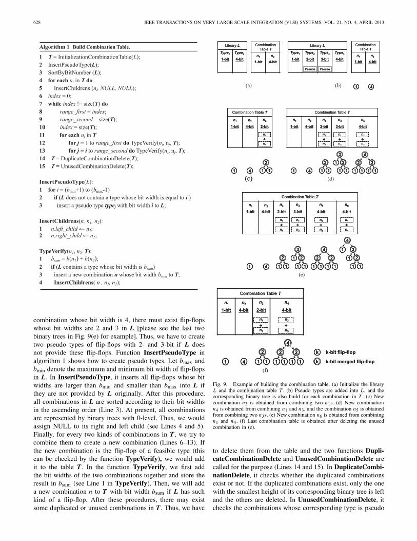
The pseudo code for building a combination table T isshown in Algorithm 1. We use a binary tree to represent onecombination for simplicity. Each node in the tree denotes onetype of a flip-flop in L. The types of flip-flops denoted byleaves will constitute the type of the flip-flop in the root.For each node, the bit width of the corresponding flip-flopequals to the bit width summation of flip-flops denoted by itsleft and right child [please see Fig. 9(e) for example]. Let ni
denote one combination in T , and b(ni ) denote its bit width.In the beginning, we initialize a combination ni for each kindof flip-flops in L (see Line 1). Then, in order to representall combinations by using a binary tree, we may add pseudotypes, which denote those flip-flops that are not provided bythe library, (see Line 2). For example, assume that a libraryonly supports two kinds of flip-flops whose bit widths are 1and 4, respectively. In order to use a binary tree to denote a
628 IEEE TRANSACTIONS ON VERY LARGE SCALE INTEGRATION (VLSI) SYSTEMS, VOL. 21, NO. 4, APRIL 2013
Algorithm 1 Build Combination Table.
1 T = InitializationCombinationTable(L);2 InsertPseudoType(L);3 SortByBitNumber (L);4 for each ni in T do5 InsertChildrens (ni, NULL, NULL);6 index = 0;7 while index != size(T) do8 range_first = index;9 range_second = size(T);10 index = size(T);11 for each ni in T12 for j = 1 to range_first do TypeVerify(ni, nj, T);13 for j = i to range_second do TypeVerify(ni, nj, T);14 T = DuplicateCombinationDelete(T);15 T = UnusedCombinationDelete(T);
InsertPseudoType(L):1 for i = (bmin+1) to (bmax-1)2 if (L does not contain a type whose bit width is equal to i )3 insert a pseudo type typej with bit width i to L;
InsertChildrens(n, n1, n2):1 n.left_child ← n1;2 n.right_child ← n2;
TypeVerify(n1, n2, T):1 bsum = b(n1) + b(n2);2 if (L contains a type whose bit width is bsum) 3 insert a new combination n whose bit width bsum to T;4 InsertChildrens( n , n1, n2);
combination whose bit width is 4, there must exist flip-flopswhose bit widths are 2 and 3 in L [please see the last twobinary trees in Fig. 9(e) for example]. Thus, we have to createtwo pseudo types of flip-flops with 2- and 3-bit if L doesnot provide these flip-flops. Function InsertPseudoType inalgorithm 1 shows how to create pseudo types. Let bmax andbmin denote the maximum and minimum bit width of flip-flopsin L. In InsertPseudoType, it inserts all flip-flops whose bitwidths are larger than bmin and smaller than bmax into L ifthey are not provided by L originally. After this procedure,all combinations in L are sorted according to their bit widthsin the ascending order (Line 3). At present, all combinationsare represented by binary trees with 0-level. Thus, we wouldassign NULL to its right and left child (see Lines 4 and 5).Finally, for every two kinds of combinations in T , we try tocombine them to create a new combination (Lines 6–13). Ifthe new combination is the flip-flop of a feasible type (thiscan be checked by the function TypeVerify), we would addit to the table T . In the function TypeVerify, we first addthe bit widths of the two combinations together and store theresult in bsum (see Line 1 in TypeVerify). Then, we will adda new combination n to T with bit width bsum if L has suchkind of a flip-flop. After these procedures, there may existsome duplicated or unused combinations in T . Thus, we have
Library L
1-bit 4-bit
Type2Type1
Combination Table T
1-bit 4-bitn2n1
Library L
1-bit 2-bit 3-bit 4-bit
Type1 Type2 Type3 Type4
Pseudo Pseudo
Combination Table T
1-bit 4-bitn2n1
1 4
Combination Table T
1-bit 4-bit
n3
2-bit
n1
n1
n2n1
+
1 1 1
2
4
Combination Table T
1-bit 4-bit
n3
2-bit
n1
n1
n4
3-bit
n1
n3
n5
4-bit
n3
n3
n2n1
+
1 1 1
2
4 1 1
21
3
1 1
2
4
1 1
2
+ +
(c)
Combination Table T
1-bit 4-bit
n3
2-bit
n1
n1
n4
3-bit
n1
n3
n5
4-bit
n3
n3
n6
4-bit
n1
n4
n2n1
1 1 1
2
4 1 1
21
3
1 1
2
4
1 1
2
1 1
21
3
4
1
+ + + +
Combination Table T
1-bit 4-bit
n3
2-bit
n1
n1
n4
4-bit
n3
n3
n2n1
1 1 1
2
4 1 1
2
4
1 1
2
+ +
k k-bit flip-flop
k k-bit merged flip-flop
Library L
1-bit 4-bit
Type2Type1
Combination Table T
1-bit 4-bitn2n1
Library L
1-bit 2-bit 3-bit 4-bit
Type1 Type2 Type3 Type4
Pseudo Pseudo
Combination Table T
1-bit 4-bitn2n1
1 4(b)
Combination Table T
1-bit 4-bit
n3
2-bit
n1
n1
n2n1
+
1 1 1
2
4
Combination Table T
1-bit 4-bit
n3
2-bit
n1
n1
n4
3-bit
n1
n3
n5
4-bit
n3
n3
n2n1
+
1 1 1
2
4 1 1
21
3
1 1
2
4
1 1
2
+ +
(c) (d)
Combination Table T
1-bit 4-bit
n3
2-bit
n1
n1
n4
3-bit
n1
n3
n5
4-bit
n3
n3
n6
4-bit
n1
n4
n2n1
1 1 1
2
4 1 1
21
3
1 1
2
4
1 1
2
1 1
21
3
4
1
+ + + +
(e)
Combination Table T
1-bit 4-bit
n3
2-bit
n1
n1
n4
4-bit
n3
n3
n2n1
1 1 1
2
4 1 1
2
4
1 1
2
+ +
k k-bit flip-flop
k k-bit merged flip-flop
(f)
(a)
Fig. 9. Example of building the combination table. (a) Initialize the libraryL and the combination table T . (b) Pseudo types are added into L , and thecorresponding binary tree is also build for each combination in T . (c) Newcombination n3 is obtained from combining two n1s. (d) New combinationn4 is obtained from combining n1 and n3, and the combination n5 is obtainedfrom combining two n3s. (e) New combination n6 is obtained from combiningn1 and n4. (f) Last combination table is obtained after deleting the unusedcombination in (e).
to delete them from the table and the two functions Dupli-cateCombinationDelete and UnusedCombinationDelete arecalled for the purpose (Lines 14 and 15). In DuplicateCombi-nationDelete, it checks whether the duplicated combinationsexist or not. If the duplicated combinations exist, only the onewith the smallest height of its corresponding binary tree is leftand the others are deleted. In UnusedCombinationDelete, itchecks the combinations whose corresponding type is pseudo
SHYU et al.: EFFECTIVE AND EFFICIENT APPROACH FOR POWER REDUCTION 629
Algorithm 2 Insert Pseudo Types (optional)
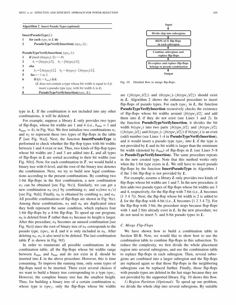
InsertPseudoType(L):1 for each typej in L do2 PseudoTypeVerifyInsertion( typej, L) ;
PseudoTypeVerifyInsertion( typej, L):1 if (mod (b(typej) /2) == 0) 2 b1 = [b(typej)/2], b2 = [b(typej)/2];3 else 4 b1 = ⎣b(typej)/2⎦, b2 = b(typej) - ⎣b(typej)/2⎦;5 for i = 1 to 26 if ((bi > bmin) &&
(L does not contain a type whose bit width is equal to bi))7 insert a pseudo type typej with bit width bi to L;8 PseudoTypeVerifyInsertion(typej, L);
type in L. If the combination is not included into any othercombinations, it will be deleted.
For example, suppose a library L only provides two typesof flip-flops, whose bit widths are 1 and 4 (i.e., bmin = 1 andbmax = 4), in Fig. 9(a). We first initialize two combinations n1and n2 to represent these two types of flip-flops in the tableT [see Fig. 9(a)]. Next, the function InsertPseudoType isperformed to check whether the flip-flop types with bit widthsbetween 1 and 4 exist or not. Thus, two kinds of flip-flop typeswhose bit widths are 2 and 3 are added into L, and all typesof flip-flops in L are sorted according to their bit widths [seeFig. 9(b)]. Now, for each combination in T , we would build abinary tree with 0-level, and the root of the binary tree denotesthe combination. Next, we try to build new legal combina-tions according to the present combinations. By combing two1-bit flip-flops in the first combination, a new combinationn3 can be obtained [see Fig. 9(c)]. Similarly, we can get anew combination n4 (n5) by combining n1 and n3(two n3’s)[see Fig. 9(d)]. Finally, n6 is obtained by combing n1 and n4.All possible combinations of flip-flops are shown in Fig. 9(e).Among these combinations, n5 and n6 are duplicated sincethey both represent the same condition, which replaces four1-bit flip-flops by a 4-bit flip-flop. To speed up our program,n6 is deleted from T rather than n5 because its height is larger.After this procedure, n4 becomes an unused combination [seeFig. 9(e)] since the root of binary tree of n4 corresponds to thepseudo type, type3, in L and it is only included in n6. Afterdeleting n6, n4 is also need to be deleted. The last combinationtable T is shown in Fig. 9(f).
In order to enumerate all possible combinations in thecombination table, all the flip-flops whose bit widths rangebetween bmax and bmin and do not exist in L should beinserted into L in the above procedure. However, this is timeconsuming. To improve the running time, only some types offlip-flops need to be inserted. There exist several choices ifwe want to build a binary tree corresponding to a type type j .However, the complete binary tree has the smallest height.Thus, for building a binary tree of a certain combination ni
whose type is type j , only the flip-flops whose bit widths
REPLACE filp-flops in each subregion
Combine subregions and replace flip-flops
De-replace and replace flip-flops belongs to pseudo combination
Divide chip into subregions
Input
Output
Fig. 10. Detailed flow to merge flip-flops.
are (�b(type j)/2�) and (b(type j)–�b(type j)/2�) should existin L. Algorithm 2 shows the enhanced procedure to insertflip-flops of pseudo types. For each type j in L, the functionPseudoTypeVerifyInsertion recursively checks the existenceof flip-flops whose bit widths around �b(type j)/2� and addthem into L if they do not exist (see Lines 1 and 2). Inthe function PseudoTypeVerifyInsertion, it divides the bitwidth b(type j) into two parts �b(type j)/2� and �b(type j )/2�(�b(type j)/2� and b(type j)–�b(type j)/2�) if b(type j ) is an even(odd) number (see Lines 1–4 in PseudoTypeVerifyInsertion),and it would insert a pseudo type type j into L if the type isnot provided by L and its bit width is larger than the minimumbit width (denoted by bmin) of flip-flops in L (see Lines 5–8in PseudoTypeVerifyInsertion). The same procedure repeatsin the new created type. Note that this method works onlywhen the 1-bit type exists in L. We still have to insert pseudoflip-flops by the function InsertPseudoType in Algorithm 1if the 1-bit flip-flop is not provided by L.
For example, assume a library L only provides two kinds offlip-flops whose bit widths are 1 and 7. In the new procedure, itfirst adds two pseudo types of flip-flops whose bit widths are 3and 4, respectively, for the flip-flop with 7-bit (i.e., L becomes[1 3 4 7]). Next, the flip-flop whose bit width is 2 is added toL for the flip-flop with 4-bit (i.e., L becomes [1 2 3 4 7]). Forthe flip-flop with 3-bit, the procedure stops because flop-flopswith 1 and 2 bits already exist in L. In the new procedure, wedo not need to insert 5- and 6-bit pseudo types to L.
C. Merge Flip-Flops
We have shown how to build a combination table inSection III-B. Now, we would like to show how to use thecombination table to combine flip-flops in this subsection. Toreduce the complexity, we first divide the whole placementregion into several subregions, and use the combination tableto replace flip-flops in each subregion. Then, several subre-gions are combined into a larger subregion and the flip-flopsare replaced again so that those flip-flops in the neighboringsubregions can be replaced further. Finally, those flip-flopswith pseudo types are deleted in the last stage because they arenot provided by the supported library. Fig. 10 shows this flow.
1) Region Partition (Optional): To speed up our problem,we divide the whole chip into several subregions. By suitable
630 IEEE TRANSACTIONS ON VERY LARGE SCALE INTEGRATION (VLSI) SYSTEMS, VOL. 21, NO. 4, APRIL 2013
subregion
chipbin
bin
bin
bin
bin
bin
Fig. 11. Example of region partition with six bins in one subregion.
partition, the computation complexity of merging flip-flops canbe reduced significantly (the related quantitative analysis willbe shown in Section V). As shown in Fig. 11, we divide theregion into several subregions, and each subregion containssix bins, where a bin is the smallest unit of a subregion.
2) Replacement of Flip-flops in Each Subregion: Beforeillustrating our procedure to merge flip-flops, we first give anequation to measure the quality if two flip-flops are going tobe replaced by a new flip-flop as follows:
cost = routing_length − α × √available_area (5)
where routing_length denotes the total routing length betweenthe new flip-flop and the pins connected to it, and avail-able_area represents the available area in the feasible regionfor placing the new flip-flop. α is a weighting factor (therelated analysis of the value α will be shown in Section V).The cost function includes the term routing_length to favora replacement that induces shorter wirelength. Besides, if theregion has larger available space to place a new flip-flop, itimplies that it has higher opportunities to combine with otherflip-flops in the future and more power reduction. Thus, wewill give it a smaller cost. Once the flip-flops cannot be mergedto a higher-bit type (as the 4-bit combination n4 in Fig. 9),we ignore the available_area in the cost function, and henceα is set to 0.
After a combination has been built, we will do the replace-ments of flip-flops according to the combination table. First,we link flip-flops below the combinations corresponding to
n11-bit
n22-bit
n34-bit
n42-bit
n1
+n1
n54-bit
n2
+n2
n64-bit
n2
+n4
n74-bit
n4
+n4
f2
f1
n11-bit
n22-bit
n34-bit
n42-bit
n1
+n1
n54-bit
n2
+n2
n64-bit
n2
+n4
n74-bit
n4
+n4
f1
f2
f3
(a) (b)
f3
f6
n11-bit
n22-bit
n34-bit
n42-bit
n1
+n1
n54-bit
n2
+n2
n64-bit
n2
+n4
n74-bit
n4
+n4
f4
f5
f3
f6
n11-bit
n22-bit
n34-bit
n42-bit
n1
+n1
n54-bit
n2
+n2
n64-bit
n2
+n4
n74-bit
n4
+n4
f7
f8
f9
(c) (d)
f3
f6
n11-bit
n22-bit
n34-bit
n42-bit
n1
+n1
n54-bit
n2
+n2
n64-bit
n2
+n4
n74-bit
n4
+n4
f9 f10
n11-bit
n22-bit
n34-bit
n42-bit
n1
+n1
n54-bit
n2
+n2
n64-bit
n2
+n4
n74-bit
n4
+n4
f9 f10
(e) (f)
Fig. 12. Example of replacements of flip-flops. (a) Sets of flip-flops beforemerging. (b) Two 1-bit flip-flops, f1 and f2, are replaced by the 2-bit flip-flopf3. (c) Two 1-bit flip-flops, f4 and f5, are replaced by the 2-bit flip-flop f6.(d) Two 2-bit flip-flops, f7 and f8, are replaced by the 4-bit flip-flop f9.(e) Two 2-bit flip-flops, f3 and f6, are replaced by the 4-bit flip-flop f10.(f) Sets of flip-flops after merging.
their types in the library. Then, for each combination n inT, we serially merge the flip-flops linked below the left childand the right child of n from leaves to root. Algorithm 3shows the procedure to get a new flip-flop corresponding tothe combination n. Based on its binary tree, we can find thecombinations associated with the left child and right child ofthe root. Hence, the flip-flops in the lists, named lleft and lright,linked below the combinations of its left child and its rightchild are checked (see Lines 2 and 3). Then, for each flip-flopf i in lleft, the best flip-flop fbest in lright, which is the flip-flopthat can be merged with f i with the smallest cost recorded incbest, is picked. For each pair of flip-flops in the respectivelist, the combination cost [based on (5)] is computed if theycan be merged and the pair with the smallest cost is chosen(see Lines 4–11). Finally, we add a new flip-flop f ′ in the listof the combination n and remove the picked flip-flops whichconstitutes the f ′ (see Lines 12–14).
For example, given a library containing three types of flip-flops (1-, 2-, and 4-bit), we first build a combination table Tas shown in Fig. 12(a). In the beginning, the flip-flops withvarious types are, respectively, linked below n1, n2, and n3 in
SHYU et al.: EFFECTIVE AND EFFICIENT APPROACH FOR POWER REDUCTION 631
SubregionNew subregionafter combination
(a) (b)
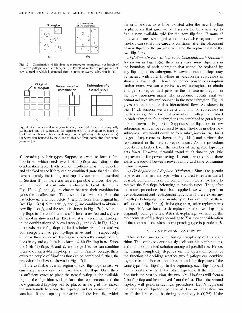
Fig. 13. Combination of flip-flops near subregion boundaries. (a) Result ofreplace flip-flops in each subregion. (b) Result of replace flip-flops in eachnew subregion which is obtained from combining twelve subregion in (a).
Original subregion Subregion after
combinationSubregion after
combination
(a) (b) (c)
Fig. 14. Combination of subregions to a larger one. (a) Placement is originallypartitioned into 16 subregions for replacement. (b) Subregion bounded bybold line is obtained from combining four neighboring subregions in (a).(c) Subregion bounded by bold line is obtained from combining four subre-gions in (b).
T according to their types. Suppose we want to form a flip-flop in n4, which needs two 1-bit flip-flops according to thecombination table. Each pair of flip-flops in n1 are selectedand checked to see if they can be combined (note that they alsohave to satisfy the timing and capacity constraints describedin Section II). If there are several possible choices, the pairwith the smallest cost value is chosen to break the tie. InFig. 12(a), f1 and f2 are chosen because their combinationgains the smallest cost. Thus, we add a new node f3 in thelist below n4, and then delete f1 and f2 from their original list[see Fig. 12(b)]. Similarly, f4 and f5 are combined to obtain anew flip-flop f6, and the result is shown in Fig. 12(c). After allflip-flops in the combinations of 1-level trees (n4 and n5) areobtained as shown in Fig. 12(d), we start to form the flip-flopsin the combinations of 2-level trees (n6, and n7). In Fig. 12(e),there exist some flip-flops in the lists below n2 and n4, and wewill merge them to get flip-flops in n6 and n7, respectively.Suppose there is no overlap region between the couple of flip-flops in n2 and n4. It fails to form a 4-bit flip-flop in n6. Sincethe 2-bit flip-flops f3 and f6 are mergeable, we can combinethem to obtain a 4-bit flip-flop f10 in n7. Finally, because thereexists no couple of flip-flops that can be combined further, theprocedure finishes as shown in Fig. 12(f).
If the available overlap region of two flip-flops exists, wecan assign a new one to replace those flip-flops. Once thereis sufficient space to place the new flip-flop in the availableregion, the algorithm will perform the replacement, and thenew generated flip-flop will be placed in the grid that makesthe wirelength between the flip-flop and its connected pinssmallest. If the capacity constraint of the bin, Bk , which
the grid belongs to will be violated after the new flip-flopis placed on that grid, we will search the bins near Bk tofind a new available grid for the new flip-flop. If none ofbins which are overlapped with the available region of newflip-flop can satisfy the capacity constraint after the placementof new flip-flop, the program will stop the replacement of thetwo flip-flops.
3) Bottom-Up Flow of Subregion Combinations (Optional):As shown in Fig. 13(a), there may exist some flip-flops inthe boundary of each subregion that cannot be replaced byany flip-flop in its subregion. However, these flip-flops maybe merged with other flip-flops in neighboring subregions asshown in Fig. 13(b). Hence, to reduce power consumptionfurther more, we can combine several subregions to obtaina larger subregion and perform the replacement again inthe new subregion again. The procedure repeats until wecannot achieve any replacement in the new subregion. Fig. 14gives an example for this hierarchical flow. As shown inFig. 14(a), suppose we divide a chip into 16 subregions inthe beginning. After the replacement of flip-flops is finishedin each subregion, four subregions are combined to get a largerone as shown in Fig. 14(b). Suppose some flip-flops in newsubregions still can be replaced by new flip-flops in other newsubregions, we would combine four subregions in Fig. 14(b)to get a larger one as shown in Fig. 14(c) and perform thereplacement in the new subregion again. As the procedurerepeats in a higher level, the number of mergeable flip-flopsgets fewer. However, it would spend much time to get littleimprovement for power saving. To consider this issue, thereexists a trade-off between power saving and time consumingin our program.
4) De-Replace and Replace (Optional): Since the pseudotype is an intermediate type, which is used to enumerate allpossible combinations in the combination table T , we have toremove the flip-flops belonging to pseudo types. Thus, afterthe above procedures have been applied, we would performde-replacement and replacement functions if there exists anyflop-flops belonging to a pseudo type. For example, if therestill exists a flip-flop, fi , belonging to n3 after replacementsin Fig. 9(f), we have to de-replace fi into two flip-flopsoriginally belongs to n1. After de-replacing, we will do thereplacements of flip-flops according to T without considerationof the combinations whose corresponding type is pseudo in L.
IV. COMPUTATION COMPLEXITY
This section analyzes the timing complexity of this algo-rithm. The core is to continuously seek suitable combinations,and find the optimized solution among all possibilities. Hence,the timing complexity depends on the operation count ofthe function of deciding whether two flip-flops can combinetogether or not. For example, assume all flip-flops are of thesame type, 1-bit flip-flop. In the beginning, each flip-flop willtry to combine with all the other flip-flops. If the first flip-flop finds the best solution, the two 1-bit flip-flops will form a2-bit flip-flop and be removed from the list. Then, the secondflip-flop will perform identical procedures. Let N representthe number of flip-flops per circuit. For an exhaustive runfor all the 1-bit cells, the timing complexity is O(N2). If the
632 IEEE TRANSACTIONS ON VERY LARGE SCALE INTEGRATION (VLSI) SYSTEMS, VOL. 21, NO. 4, APRIL 2013
0 5 1078.779.5
80.381.1
81.9
82.7
83.5
Number of FFs
in single region (104)
Pow
er (N
orm
aliz
ed)
(%)
0 5 100
25
50
75
100
Number of FFs
in single region (104)
Exec
u�on
Tim
e(N
orm
aliz
ed) (
%)
(a) (b)
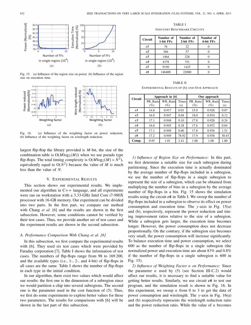
Fig. 15. (a) Influence of the region size on power. (b) Influence of the regionsize on execution time.
0 0.5 1 1.5 2 2.5 35
6
7
8
9
10
11
12
13
Weigh�ng factor
Wire
-leng
th re
duce
d(N
orm
aliz
ed) (
%)
0 1 2 320.9
20.95
21
21.05
21.1
21.15
21.2
21.25
21.3
Weigh�ng factor
Pow
er re
duce
d (N
orm
aliz
ed)(
%)
(a) (b)
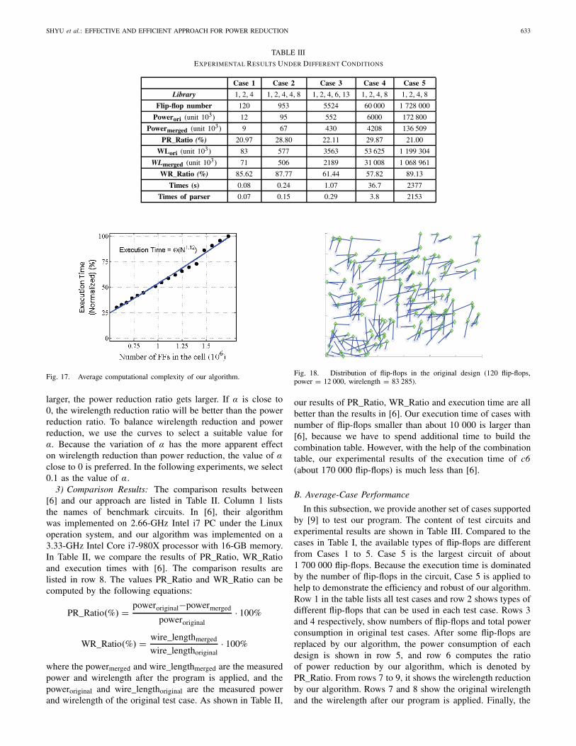
Fig. 16. (a) Influence of the weighting factor on power reduction.(b) Influence of the weighting factor on wirelength reduction.
largest flip-flop the library provided is M-bit, the size of thecombination table is O(Mlog2(M)) when we use pseudo typeflip-flops. The total timing complexity is O(Mlog2(M)× N2),equivalently equal to O(N2) because the value of M is muchless than the value of N .
V. EXPERIMENTAL RESULTS
This section shows our experimental results. We imple-mented our algorithm in C++ language, and all experimentswere ran on workstation with a 3.33-GHz Intel Core i7-980Xprocessor with 16-GB memory. Our experiment can be dividedinto two parts. In the first part, we compare our methodwith Chang et al. [6] and the results are shown in the firstsubsection. However, some conditions cannot be verified bytheir test cases. Thus, we provide another set of test cases andthe experiment results are shown in the second subsection.
A. Performance Comparison With Chang et al. [6]
In this subsection, we first compare the experimental resultswith [6]. They used six test cases which were provided byFaraday corporation [7]. Table I shows the information of testcases. The numbers of flip-flops range from 98 to 169 200,and the available types (i.e., 1-, 2-, and 4-bit) of flip-flops inall cases are the same. Table I shows the number of flip-flopsin each type in the initial condition.
In our algorithm, there exist two values which would affectour results: the first one is the dimension of a subregion sincewe would partition a chip into several subregions. The secondone is the parameter used in the cost function of (5). Thus,we first do some experiments to explore better values for thesetwo parameters. The results for comparisons with [6] will beshown in the last part of this subsection.
TABLE I
INDUSTRY BENCHMARK CIRCUITS
Circuit Number of1-bit FFs
Number of2-bit FFs
Number of4-bit FFs
c1 76 22 0
c2 366 57 0
c3 1464 228 0
c4 4378 751 0
c5 9150 1425 0
c6 146400 22800 0
TABLE II
EXPERIMENTAL RESULTS OF [6] AND OUR APPROACH
CircuitApproach in [6] Our approach
PR_Ratio(%)
WR_Ratio(%)
Times(s)
PR_Ratio(%)
WR_Ratio(%)
Times(s)
c1 14.8 0.917 0.01 15.9 0.928 0.07
c2 16.9 0.947 0.04 18.0 0.934 0.12
c3 17.1 0.948 0.10 17.8 0.928 0.24
c4 16.8 0.945 0.28 17.6 0.932 0.84
c5 17.1 0.949 0.60 17.8 0.936 1.51
c6 17.2 0.949 78.92 17.9 0.938 30.43
Comp. 0.95 1.01 2.41 1.00 1.00 1.00
1) Influence of Region Size on Performance: In this part,we first determine a suitable size for each subregion duringpartitioning. Since the execution time is actually dominatedby the average number of flip-flops included in a subregion,we use the number of flip-flops in a single subregion torepresent the size of a subregion, which can be obtained frommultiplying the number of bins in a subregion by the averagenumber of flip-flops in a bin. Fig. 15 shows the simulationresults using the circuit c6 in Table I. We sweep the number offlip-flops included in a subregion to observe its effect on powerconsumption and execution time. The y-axis in Fig. 15(a)and (b), respectively, represent the power reduction and tim-ing improvement ratios relative to the size of a subregion.While a subregion gets larger, the execution time becomeslonger. However, the power consumption does not decreaseproportionally. On the contrary, if the subregion size becomesvery small, the power consumption will increase significantly.To balance execution time and power consumption, we select600 as the number of flip-flops in a single subregion (thenormalized power and execution time are about 83% and 0.8%if the number of flip-flops in a single subregion is 600 inFig. 15).
2) Influence of Weighting Factor α on Performance: Sincethe parameter α used by (5) (see Section III-C.2) wouldaffect our results, it is necessary to find a suitable value forgetting better results. Similarly, we use circuit c6 to test ourprogram, and the simulation result is shown in Fig. 16. Inthis experiment, we sweep α from 0 to 3 to get the data ofpower consumption and wirelength. The y-axis in Fig. 16(a)and (b) respectively represents the wirelength reduction ratioand the power reduction ratio. While the value of α becomes
SHYU et al.: EFFECTIVE AND EFFICIENT APPROACH FOR POWER REDUCTION 633
TABLE III
EXPERIMENTAL RESULTS UNDER DIFFERENT CONDITIONS
Case 1 Case 2 Case 3 Case 4 Case 5
Library 1, 2, 4 1, 2, 4, 4, 8 1, 2, 4, 6, 13 1, 2, 4, 8 1, 2, 4, 8
Flip-flop number 120 953 5524 60 000 1 728 000
Powerori (unit 103) 12 95 552 6000 172 800
Powermerged (unit 103) 9 67 430 4208 136 509
PR_Ratio (%) 20.97 28.80 22.11 29.87 21.00
WLori (unit 103) 83 577 3563 53 625 1 199 304
WLmerged (unit 103) 71 506 2189 31 008 1 068 961
WR_Ratio (%) 85.62 87.77 61.44 57.82 89.13
Times (s) 0.08 0.24 1.07 36.7 2377
Times of parser 0.07 0.15 0.29 3.8 2153
Fig. 17. Average computational complexity of our algorithm.
larger, the power reduction ratio gets larger. If α is close to0, the wirelength reduction ratio will be better than the powerreduction ratio. To balance wirelength reduction and powerreduction, we use the curves to select a suitable value forα. Because the variation of α has the more apparent effecton wirelength reduction than power reduction, the value of αclose to 0 is preferred. In the following experiments, we select0.1 as the value of α.
3) Comparison Results: The comparison results between[6] and our approach are listed in Table II. Column 1 liststhe names of benchmark circuits. In [6], their algorithmwas implemented on 2.66-GHz Intel i7 PC under the Linuxoperation system, and our algorithm was implemented on a3.33-GHz Intel Core i7-980X processor with 16-GB memory.In Table II, we compare the results of PR_Ratio, WR_Ratioand execution times with [6]. The comparison results arelisted in row 8. The values PR_Ratio and WR_Ratio can becomputed by the following equations:
PR_Ratio(%) = poweroriginal−powermerged
poweroriginal· 100%
WR_Ratio(%) = wire_lengthmerged
wire_lengthoriginal· 100%
where the powermerged and wire_lengthmerged are the measuredpower and wirelength after the program is applied, and thepoweroriginal and wire_lengthoriginal are the measured powerand wirelength of the original test case. As shown in Table II,
Fig. 18. Distribution of flip-flops in the original design (120 flip-flops,power = 12 000, wirelength = 83 285).
our results of PR_Ratio, WR_Ratio and execution time are allbetter than the results in [6]. Our execution time of cases withnumber of flip-flops smaller than about 10 000 is larger than[6], because we have to spend additional time to build thecombination table. However, with the help of the combinationtable, our experimental results of the execution time of c6(about 170 000 flip-flops) is much less than [6].
B. Average-Case Performance
In this subsection, we provide another set of cases supportedby [9] to test our program. The content of test circuits andexperimental results are shown in Table III. Compared to thecases in Table I, the available types of flip-flops are differentfrom Cases 1 to 5. Case 5 is the largest circuit of about1 700 000 flip-flops. Because the execution time is dominatedby the number of flip-flops in the circuit, Case 5 is applied tohelp to demonstrate the efficiency and robust of our algorithm.Row 1 in the table lists all test cases and row 2 shows types ofdifferent flip-flops that can be used in each test case. Rows 3and 4 respectively, show numbers of flip-flops and total powerconsumption in original test cases. After some flip-flops arereplaced by our algorithm, the power consumption of eachdesign is shown in row 5, and row 6 computes the ratioof power reduction by our algorithm, which is denoted byPR_Ratio. From rows 7 to 9, it shows the wirelength reductionby our algorithm. Rows 7 and 8 show the original wirelengthand the wirelength after our program is applied. Finally, the
634 IEEE TRANSACTIONS ON VERY LARGE SCALE INTEGRATION (VLSI) SYSTEMS, VOL. 21, NO. 4, APRIL 2013
Fig. 19. Resulting distribution of flip-flops (34 flip-flops, power = 9484,wirelength = 71 304)
Fig. 20. Distribution of flip-flops in the original design. (5524 flip-flops,power = 552 400, wirelength = 3 562 985).
ratio of wirelength reduction, which is denoted by WR_Ratio,is shown in row 9.
The values of PR_Ratio in all cases are between 20 and 30.Besides, the wirelength are less than the original circuit in allcases, and the best value of WR_Ratio can achieve 42.18%improvement. Row 10 shows the execution time of each case.Because of the long execution time of parser, we show theexecution time of parser in row 11.
Fig. 17 displays the curve of the execution time with respectto various flip-flop numbers in a circuit. The test cases areobtained by duplicating Case 1 various times. The x-axisrepresents the number of flip-flops, and the y-axis denotesthe percentage of a execution time compared with the longestexecution time. As the number of flip-flops increases, theexecution time of parser will be longer than execution timewhich does not include parser. For this reason, the executiontime in Fig. 17 does not include the execution time of parser.The largest case, which contains about 1 700 000 flip-flops,takes the longest execution time (about 10 min). According toFig. 17, it shows that the timing complexity of our algorithmis O(N1.12) instead of O(N2).
Figs. 18 and 19 show the original distribution of flip-flopsand the resulting distribution of flip-flops after applying ourprogram. In the figures, flip-flops are denoted by green circlesand pins by blue circles. Blue lines represent the wires that
Fig. 21. Resulting distribution of flip-flops. (1378 flip-flops, power =430 260, wirelength = 2 189 215).
connect pins and flip-flops. In Fig. 18, there are 120 1-bitflip-flops and 240 pins in the original circuit in Case 1. Afterapplying our program, there only exist 27 4-bit flip-flops, five2-bit flip-flops and two 1-bit flip-flops in the new design shownin Fig. 19. In Fig. 20, there exist 5524 2-bit flip-flops and11 048 pins in the original circuit in Case 3. There only existtwo 6-bit, 1284 4-bit, 34 2-bit, and eight 1-bit flip-flops forthe new circuit shown in Fig. 21 after applying our program.
VI. CONCLUSION
This paper has proposed an algorithm for flip-flop replace-ment for power reduction in digital integrated circuit design.The procedure of flip-flop replacements is depending on thecombination table, which records the relationships among theflip-flop types. The concept of pseudo type is introduced tohelp to enumerate all possible combinations in the combinationtable. By the guidelines of replacements from the combina-tion table, the impossible combinations of flip-flops will notbe considered that decreases execution time. Besides powerreduction, the objective of minimizing the total wirelengthalso be considered to the cost function. The experimentalresults show that our algorithm can achieve a balance betweenpower reduction and wirelength reduction. Moreover, evenfor the largest case which contains about 1 700 000 flip-flops,our algorithm can maintain the performance of power andwirelength reduction in the reasonable processing time.
REFERENCES
[1] P. Gronowski, W. J. Bowhill, R. P. Preston, M. K. Gowan, and R. L.Allmon, “High-performance microprocessor design,” IEEE J. Solid-StateCircuits, vol. 33, no. 5, pp. 676–686, May 1998.
[2] W. Hou, D. Liu, and P.-H. Ho, “Automatic register banking for low-power clock trees,” in Proc. Quality Electron. Design, San Jose, CA,Mar. 2009, pp. 647–652.
[3] D. Duarte, V. Narayanan, and M. J. Irwin, “Impact of technology scalingin the clock power,” in Proc. IEEE VLSI Comput. Soc. Annu. Symp.,Pittsburgh, PA, Apr. 2002, pp. 52–57.
[4] H. Kawagachi and T. Sakurai, “A reduced clock-swing flip-flop (RCSFF)for 63% clock power reduction,” in VLSI Circuits Dig. Tech. PapersSymp., Jun. 1997, pp. 97–98.
[5] Y. Cheon, P.-H. Ho, A. B. Kahng, S. Reda, and Q. Wang, “Power-awareplacement,” in Proc. Design Autom. Conf., Jun. 2005, pp. 795–800.

SHYU et al.: EFFECTIVE AND EFFICIENT APPROACH FOR POWER REDUCTION 635
[6] Y.-T. Chang, C.-C. Hsu, P.-H. Lin, Y.-W. Tsai, and S.-F. Chen,“Post-placement power optimization with multi-bit flip-flops,” in Proc.IEEE/ACM Comput.-Aided Design Int. Conf., San Jose, CA, Nov. 2010,pp. 218–223.
[7] Faraday Technology Corporation [Online]. Available: http://www.faraday-tech.com/index.html
[8] C. Bron and J. Kerbosch, “Algorithm 457: Finding all cliques of anundirected graph,” ACM Commun., vol. 16, no. 9, pp. 575–577, 1973.
[9] CAD Contest of Taiwan [Online]. Available: http://cad_contest.cs.nctu.edu.tw/cad11
Ya-Ting Shyu received the M.S. degree in electricalengineering from National Cheng Kung University(NCKU), Tainan, Taiwan, in 2008, where she ispursuing the Ph.D. degree in electronic engineering.
Her current research interests include integratedcircuit design, design automation for analog, andmixed-signal circuits.
Jai-Ming Lin received the B.S., M.S., and Ph.D.degrees from National Chiao Tung University,Hsinchu, Taiwan, in 1996, 1998, and 2002, respec-tively, all in computer science.
He was an Assistant Project Leader with the CADTeam, Realtek Corporation, Hsinchu, from 2002 to2007. He is currently an Assistant Professor withthe Department of Electrical Engineering, NationalCheng Kung University, Tainan, Taiwan. His currentresearch interests include floorplan, placement, rout-ing, and clock tree synthesis.
Chun-Po Huang was born in Tainan, Taiwan, in1986. He received the B.S. degree in electricalengineering from National Cheng Kung University,Tainan, Taiwan, in 2008, where he is currentlypursuing the Ph.D. degree in electronic engineering.
His current research interests include designautomation for high-speed and low-power analog-to-digital converters.
Cheng-Wu Lin received the M.S. degree in elec-trical engineering from National Cheng Kung Uni-versity (NCKU), Tainan, Taiwan, in 2006, where heis currently pursuing the Ph.D. degree in electronicengineering.
His current research interests include integratedcircuit design, design automation for analog, andmixed-signal circuits.
Ying-Zu Lin received the B.S. and M.S. degreesin electrical engineering and the Ph.D. degree fromNational Cheng Kung University, Tainan, Taiwan, in2003, 2005, and 2010, respectively.
He is currently with Novatek, Hsinchu, Taiwan,a Senior Engineer, where he is working on high-speed interfaces and analog circuits for advanceddisplay systems. His current research interestsinclude analog/mixed-signal circuits, analog-to-digital converters, and high-speed interface cir-cuits.
Dr. Lin was the recipient of the Excellent Award in the master thesiscontest held by the Mixed-Signal and Radio-Frequency Consortium, Taiwan,in 2005, the Best Paper Award of the VLSI Design/Computer-Aided DesignSymposium, Taiwan, in 2008, and the Taiwan Semiconductor ManufacturingCompany Outstanding Student Research Award. He received third prize in theAcer Dragon Award for Excellence. He was the recipient of the MediaTekFellowship in 2009, the Best Paper Award from the Institute of Electronics,Information, and Communication Engineers, and the Best Ph.D. Award fromthe IEEE Tainan Section in 2010. He was a co-recipient of the Gold Award inMacronix Golden Silicon Design Contests in 2010. He was a recipient of theInternational Solid State Circuits Conference/Design Automation ConferenceStudent Design Contest in 2011, the Chip Implementation Center OutstandingChip Design Award (Best Design), and the International Symposium ofIntegrated Circuits Chip Design Competition.
Soon-Jyh Chang (M’03) was born in Tainan,Taiwan, in 1969. He received the B.S. degree inelectrical engineering from National Central Uni-versity, Jhongli, Taiwan, in 1991, and the M.S.and Ph.D. degrees in electronic engineering fromNational Chiao Tung University, Hsinchu, Taiwan,in 1996 and 2002, respectively.
He has been with the Department of Electri-cal Engineering, National Cheng Kung University,Tainan, since 2003, where he is currently a Professorand the Director of the Electrical Laboratories since
2011. He has authored or co-authored over 100 technical papers and 7 patents.His current research interests include design, testing, and design automationfor analog and mixed-signal circuits.
Dr. Chang has been serving as the Chair of the IEEE Solid-State CircuitsSociety Tainan Chapter since 2009. He was the Technical Program Co-Chair of the IEEE Institute for Sustainable Nanoelectronics in 2010, andthe Committee Member of the IEEE Asian Test Symposium in 2009, Asiaand South Pacific Design Automation Conference in 2010, the VLSI-Design,Automation, and Test in 2009, 2010, and 2012, and the Asian Solid-StateCircuits Conference in 2009 and 2011. He was a recipient and co-recipient ofmany technical awards, including the Greatest Achievement Award from theNational Science Council, Taiwan, in 2007, the Chip Implementation CenterOutstanding Chip Award in 2008, 2011, and 2012, the Best Paper Awardof VLSI Design/Computer-Aided Design Symposium, Taiwan, in 2009 and2010, the Best Paper Award of the Institute of Electronics, Information andCommunication Engineers in 2010, the Gold Prize of the Macronix GoldenSilicon Award in 2010, the Best GOLD Member Award from the IEEE TainanSection in 2010, the International Solid State Circuits Conference/DesignAutomation Conference Student Design Contest in 2011, and the InternationalSymposium on Integrated Circuits Chip Design Competition in 2011.