Embed Size (px)
Citation preview
Advances in Materials 2016; 5(4): 23-30 http://www.sciencepublishinggroup.com/j/am doi: 10.11648/j.am.20160504.12 ISSN: 2327-2503 (Print); ISSN: 2327-252X (Online)
Effect of Fluorine Doping on Structural and Optical Properties of SnO2 Thin Films Prepared by Chemical Spray Pyrolysis Method
Nabeel A. Bakr*, Sabah A. Salman, Mohammed N. Ali
Department of Physics, College of Science, University of Diyala, Diyala, Iraq
Email address: [email protected] (N. A. Bakr), [email protected] (N. A. Bakr) *Corresponding author
To cite this article: Nabeel A. Bakr, Sabah A. Salman, Mohammed N. Ali. Effect of Fluorine Doping on Structural and Optical Properties of SnO2 Thin Films Prepared by Chemical Spray Pyrolysis Method. Advances in Materials. Vol. 5, No. 4, 2016, pp. 23-30. doi: 10.11648/j.am.20160504.12
Received: July 3, 2016; Accepted: July 13, 2016; Published: August 17, 2016
Abstract: In this study, (SnO2-xFx) thin films where (x = 0, 0.02, 0.04, 0.06 and 0.08) have been deposited by chemical spray pyrolysis method on glass substrates at temperature of (400°C), using Tin Chloride Pentahydrate (SnCl4.5H2O) and Ammonium Fluoride (NH4F) solutions. The structural properties and morphology of these films have been studied using XRD and AFM respectively. XRD analysis showed that these films are polycrystalline in nature with tetragonal Rutile structure with preferred orientation of (110). Doping with Fluorine causes a decrease in the crystallite size. The optical properties for all the films were studied by recording the transmittance and absorbance spectra in the range of (300-900) nm. The results showed that the absorbance increases with increasing the doping percentage. The optical energy gap for allowed direct electronic transition was calculated and it was found that the thin film with 0.08 doping percentage has the least value of 3.72 eV. Urbach energy decreases with increasing doping percentage. The optical constants (absorption coefficient, refractive index, extinction coefficient, real and imaginary parts of dielectric constant) as a function of photon energy for all prepared films were calculated.
Keywords: (SnO2) Thin Films, Fluorine Doping, Chemical Spray Pyrolysis, XRD, Optical Properties
1. Introduction
Tin dioxide (SnO2), is an important n-type semiconductor with tetragonal Rutile structure having lattice parameters a = b = 4.737 Å and c = 3.826 Å. The unit cell contains two tin and four oxygen atoms. Each tin atom is bounded to six oxygen atoms at the corners of a regular octahedron, and every oxygen atom is surrounded by three tin atoms. Tin oxide has been extensively investigated for gas sensors, optical-conductive coatings for solar cells and electro catalytic anodes [1, 2], glass coatings for furnace windows as well as transparent electrodes for liquid crystal displays [3]. Tin dioxide (SnO2) has a density of (6.95 g/cm3) and molecular weight of (150.69 g/mol). Its melting point is (2643 K) [4].
F-doped tin oxide (FTO) coated glass is electrically conductive and ideal for use in a wide range of devices, including applications such as opto-electronics, touch screen displays, thin film photovoltaics, energy-saving windows,
RFI/EMI shielding and other electro-optical and insulating applications. F-doped tin oxide has been recognized as a very promising material because it is relatively stable under atmospheric conditions, chemically inert, mechanically hard, high-temperature resistant, has a high tolerance to physical abrasion and is less expensive than indium tin oxide [5, 6]. It is also applied in the field of touch panel, solar cell electrode, low-emissivity glass, defrost window, and anti-static material [7].
2. Experimental Procedure
In this study, (SnO2-xFx) thin films where (x = 0, 0.02, 0.04, 0.06 and 0.08) have been deposited by chemical spray pyrolysis (CSP) technique described elsewhere [8]. The spray solution was prepared by mixing (0.1 M) aqueous solution of Tin Chloride Pentahydrate (SnCl4.5H2O) and (0.1 M) aqueous solution of Ammonium Fluoride (NH4F) in appropriate percentages. Other deposition conditions such as
Advances in Materials 2016; 5(4): 23-30 24
spray nozzle substrate distance (30 ± 1 cm), spray time (10 s), spray interval (3 min) and pressure of the carrier gas (1.5 bar) were kept constant for each deposition. The thickness of deposited films was about 400±10 nm measured by the conventional gravimetric technique. Experiments were conducted at substrate temperature of (400°C) to investigate the effect of Fluorine doping on the growth of the films keeping other parameters constant. The X ray diffraction patterns for the prepared films were obtained by (Ultima IV X-ray diffractometer) goniometer using copper target (Cu, 1.5416 Å, Focus size 0.4 X 12 mm) and Atomic Force Microscopy (AFM) micrographs were recorded by using scanning probe microscope type (SPM-AA3000), contact mode, supplied by Angstrom Advanced Inc. Optical properties in the wavelength range of (300 - 900) nm were investigated by using UV-VIS-NIR spectroscopy (Shimadzu, UV-1800).
3. Results and Discussion
3.1. Structural Analysis
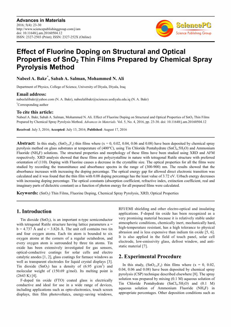
The X-ray diffraction patterns of undoped and F doped SnO2 deposited at 400°C are shown in Figure (1). The highest four diffraction peaks are (110), (101), (200) and (211), which are in agreement with the International Centre for Diffraction Data (ICDD) card number (41-1445) with a tetragonal unit cell showing a preferred orientation along (110). F doping led to a decrease in the intensity of the diffraction peaks.
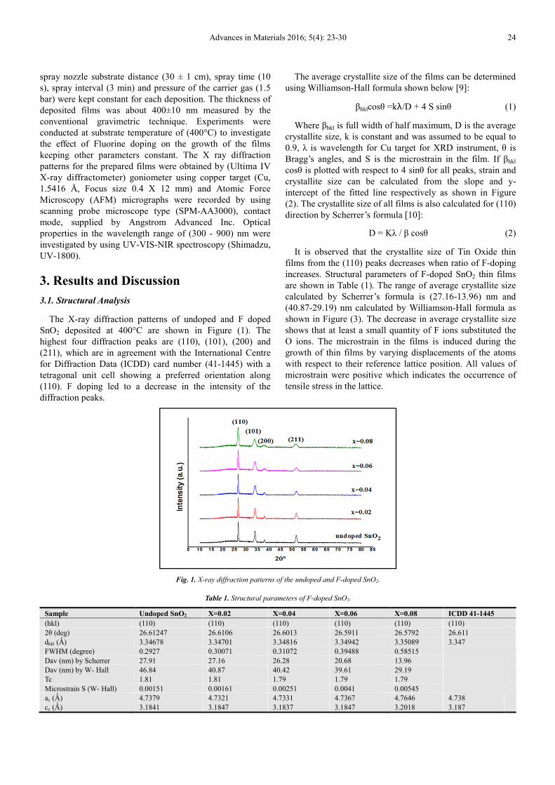
The average crystallite size of the films can be determined using Williamson-Hall formula shown below [9]:
βhklcosθ =kλ/D + 4 S sinθ (1)
Where βhkl is full width of half maximum, D is the average crystallite size, k is constant and was assumed to be equal to 0.9, λ is wavelength for Cu target for XRD instrument, θ is Bragg’s angles, and S is the microstrain in the film. If βhkl cosθ is plotted with respect to 4 sinθ for all peaks, strain and crystallite size can be calculated from the slope and y-intercept of the fitted line respectively as shown in Figure (2). The crystallite size of all films is also calculated for (110) direction by Scherrer’s formula [10]:
D = Kλ / β cosθ (2)
It is observed that the crystallite size of Tin Oxide thin films from the (110) peaks decreases when ratio of F-doping increases. Structural parameters of F-doped SnO2 thin films are shown in Table (1). The range of average crystallite size calculated by Scherrer’s formula is (27.16-13.96) nm and (40.87-29.19) nm calculated by Williamson-Hall formula as shown in Figure (3). The decrease in average crystallite size shows that at least a small quantity of F ions substituted the O ions. The microstrain in the films is induced during the growth of thin films by varying displacements of the atoms with respect to their reference lattice position. All values of microstrain were positive which indicates the occurrence of tensile stress in the lattice.
Fig. 1. X-ray diffraction patterns of the undoped and F-doped SnO2.
Table 1. Structural parameters of F-doped SnO2.
Sample Undoped SnO2 X=0.02 X=0.04 X=0.06 X=0.08 ICDD 41-1445
(hkl) (110) (110) (110) (110) (110) (110) 2θ (deg) 26.61247 26.6106 26.6013 26.5911 26.5792 26.611 dhkl (Ǻ) 3.34678 3.34701 3.34816 3.34942 3.35089 3.347 FWHM (degree) 0.2927 0.30071 0.31072 0.39488 0.58515
Dav (nm) by Scherrer 27.91 27.16 26.28 20.68 13.96
Dav (nm) by W- Hall 46.84 40.87 40.42 39.61 29.19
Tc 1.81 1.81 1.79 1.79 1.79
Microstrain S (W- Hall) 0.00151 0.00161 0.00251 0.0041 0.00545
ao (Ǻ) 4.7379 4.7321 4.7331 4.7367 4.7646 4.738
co (Ǻ) 3.1841 3.1847 3.1837 3.1847 3.2018 3.187
25 Nabeel A. Bakr et al.: Effect of Fluorine Doping on Structural and Optical Properties of SnO2 Thin Films Prepared by Chemical Spray Pyrolysis Method
Fig. 2. W-H analysis for undoped and F-doped SnO2 thin films.
The texture coefficient (Tc) represents the texture of a particular plane, in which greater than unity values imply that there are numerous of grains in that particular direction. The texture coefficients Tc (hkl) for all samples have been calculated from the X-ray data using the well-known formula [11]:
���ℎ��� = ���� ����⁄���∑���� ����⁄ (3)
Where I (hkl) is the measured intensity, Io (hkl) taken from the ICDD standard data, (N) is the number of peaks and (hkl) are Miller indices. The texture coefficient is calculated for crystal plane (110) of the undoped and (SnO2-xFx) films. All values of texture coefficient were greater than 1 which indicate the abundance of grains in the (110) direction.
3.2. (AFM) Results
The 3D AFM micrographs of the undoped and F-doped
1.6 1.8 2.0 2.2 2.4 2.6 2.8 3.0 3.2 3.4
0.004
0.005
0.006
0.007
0.008
0.009
0.010
βco
s(θ
)
4sin(θ)
y = 0.0034 + 0.00161 x
x = 0.02
1.6 1.8 2.0 2.2 2.4 2.6 2.8 3.0 3.2 3.4
0.004
0.006
0.008
0.010
0.012
0.014
βco
s(θ
)
4sin(θ)
y = 0.00343 + 0.00251 x
X = 0.04
1.6 1.8 2.0 2.2 2.4 2.6 2.8 3.0 3.2 3.4
0.004
0.006
0.008
0.010
0.012
0.014
0.016
0.018
0.020
βco
s(θ
)
4sin(θ)
y = 0.0035 + 0.0041 x
x = 0.06
1.6 1.8 2.0 2.2 2.4 2.6 2.8 3.0 3.2 3.4
0.0040
0.0045
0.0050
0.0055
0.0060
0.0065
0.0070
0.0075
0.0080
0.0085
βco
s(θ
)
4sin(θ)
y = 0.00296 + 0.00151 x
Undoped SnO2
1.6 1.8 2.0 2.2 2.4 2.6 2.8 3.0 3.2 3.4
0.006
0.008
0.010
0.012
0.014
0.016
0.018
0.020
0.022
0.024
0.026
0.028
βcos(θ
)
4sin(θ)
y = 0.00475 + 0.00545 x
x = 0.08

Advances in Materials 2016; 5(4): 23-30 26
SnO2 thin films are shown in Figure (4). The size of the scanned area was (2 X 2) µm2. AFM results show homogenous and smooth thin films. The average grain size, average roughness and root mean square (RMS) roughness for all samples estimated from AFM are given in Table (2).
Fig. 3. Average crystallite size as a function of doping percentage.
Table 2. The grain size of undoped and F doped SnO2 thin films.
Sample T=400°C Surface Roughness
(nm) RMS (nm)
Grain Size
(nm)
Undoped SnO2 1.88 2.20 112.12
SnO1.98F0.02 1.84 2.11 105.40
SnO1.96F0.04 1.81 2.10 101.81
SnO1.94F0.06 1.56 1.82 95.81
SnO1.92F0.08 1.48 1.76 86.81
Fig. 4. 3D AFM images of undoped and F-doped SnO2 thin films.
3.3. Optical Properties
The transmittance spectra of the undoped and F-doped SnO2 thin films with doping percentage (x = 0.02, 0.04, 0.06 and 0.08) are shown in figure (5). It can be seen that the transmittance of the films decreases with increasing the doping percentage and the highest value of transmittance (0.95). This is due to the formation of new localized levels which are capable to receive electrons and generate localized energy tails inside the optical energy gap which work on the absorption of low energy photons thus will increase absorbance and decrease transmittance.
Fig. 5. Transmittance spectra of the undoped and F-doped SnO2 films.
The absorbance spectra of the undoped and F-doped SnO2 thin are shown in figure (6). It is clear that the absorbance increases with increasing the doping percentage because of the incorporation of Fluorine within the crystal structure of the prepared films [12]. The absorbance decreases rapidly at short wavelengths.
Fig. 6. Absorbance spectra of the undoped and F-doped SnO2 films.
The following relation can be used for calculating the reflectance (R) [13]:
R+A+T =1 (4)
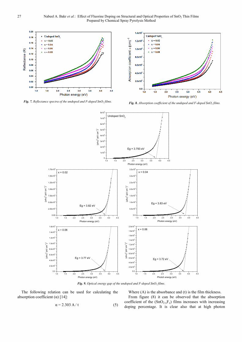
Figure (7) shows the reflectance as a function of the photon energy of the films with different doping percentages.
27 Nabeel A. Bakr et al.: Effect of Fluorine Doping on Structural and Optical Properties of SnO2 Thin Films Prepared by Chemical Spray Pyrolysis Method
Fig. 7. Reflectance spectra of the undoped and F-doped SnO2 films.
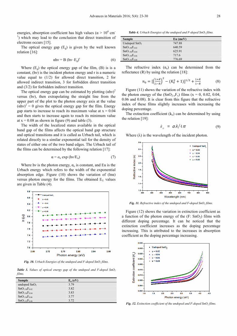
Fig. 8. Absorption coefficient of the undoped and F-doped SnO2 films.
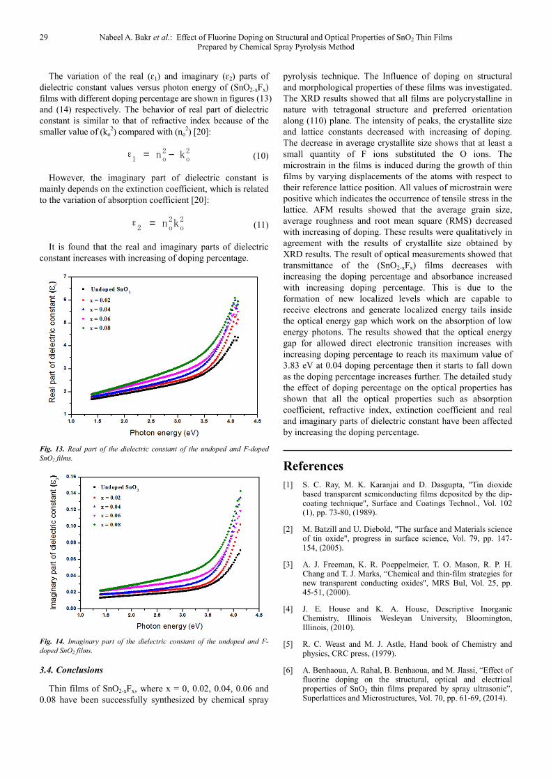
Fig. 9. Optical energy gap of the undoped and F-doped SnO2 films.
The following relation can be used for calculating the absorption coefficient (α) [14]:
α = 2.303 A / t (5)
Where (A) is the absorbance and (t) is the film thickness. From figure (8) it can be observed that the absorption
coefficient of the (SnO2-xFx) films increases with increasing doping percentage. It is clear also that at high photon
1.0 1.5 2.0 2.5 3.0 3.5 4.0 4.5
0
1x10⁸
2x10⁸
3x10⁸
4x10⁸
5x10⁸
6x10⁸
7x10⁸
8x10⁸
(αh
ν)2 (
eV
cm
-1)2
Photon energy (eV)
Eg = 3.793 eV
Undoped SnO2
1.0 1.5 2.0 2.5 3.0 3.5 4.0 4.5
0.00
2.50x10⁸
5.00x10⁸
7.50x10⁸
1.00x10⁹
1.25x10⁹
1.50x10⁹
1.75x10⁹
Eg = 3.82 eV
(αh
ν)2 (
eV
cm
-1)2
Photon energy (eV)
x = 0.02
1.0 1.5 2.0 2.5 3.0 3.5 4.0 4.5
0.0
5.0x10⁸
1.0x10⁹
1.5x10⁹
2.0x10⁹
2.5x10⁹
3.0x10⁹
3.5x10⁹
x = 0.04
(αh
ν)2 (
eV
cm
-1)2
Photon energy (eV)
Eg = 3.83 eV
1.0 1.5 2.0 2.5 3.0 3.5 4.0 4.5
0.0
2.0x10⁸
4.0x10⁸
6.0x10⁸
8.0x10⁸
1.0x10⁹
1.2x10⁹
1.4x10⁹
1.6x10⁹
Photon energy (eV)
x = 0.06
(αh
ν)2 (
eV
cm
-1)2
Eg = 3.77 eV
1.0 1.5 2.0 2.5 3.0 3.5 4.0 4.5
0.0
2.0x10⁸
4.0x10⁸
6.0x10⁸
8.0x10⁸
1.0x10⁹
1.2x10⁹
1.4x10⁹
1.6x10⁹
1.8x10⁹
2.0x10⁹
x = 0.06
(αh
ν)2 (
eV
cm
-1)2
Photoh energy (eV)
Eg = 3.72 eV
Advances in Materials 2016; 5(4): 23-30 28
energies, absorption coefficient has high values (α > 104 cm-
1) which may lead to the conclusion that direct transition of electrons occurs [15].
The optical energy gap (Eg) is given by the well known relation [16]:
αhν = B (hν–Eg)r (6)
Where (Eg) the optical energy gap of the film, (B) is is a constant, (hν) is the incident photon energy and r is a numeric value equal to (1/2) for allowed direct transition, 2 for allowed indirect transition, 3 for forbidden direct transition and (3/2) for forbidden indirect transition.
The optical energy gap can be estimated by plotting (αhν)2 versus (hν), then extrapolating the straight line from the upper part of the plot to the photon energy axis at the value (αhν)2 = 0 gives the optical energy gap for the film. Energy gap starts to increase to reach its maximum value at x = 0.04 and then starts to increase again to reach its minimum value at x = 0.08 as shown in figure (9) and table (3).
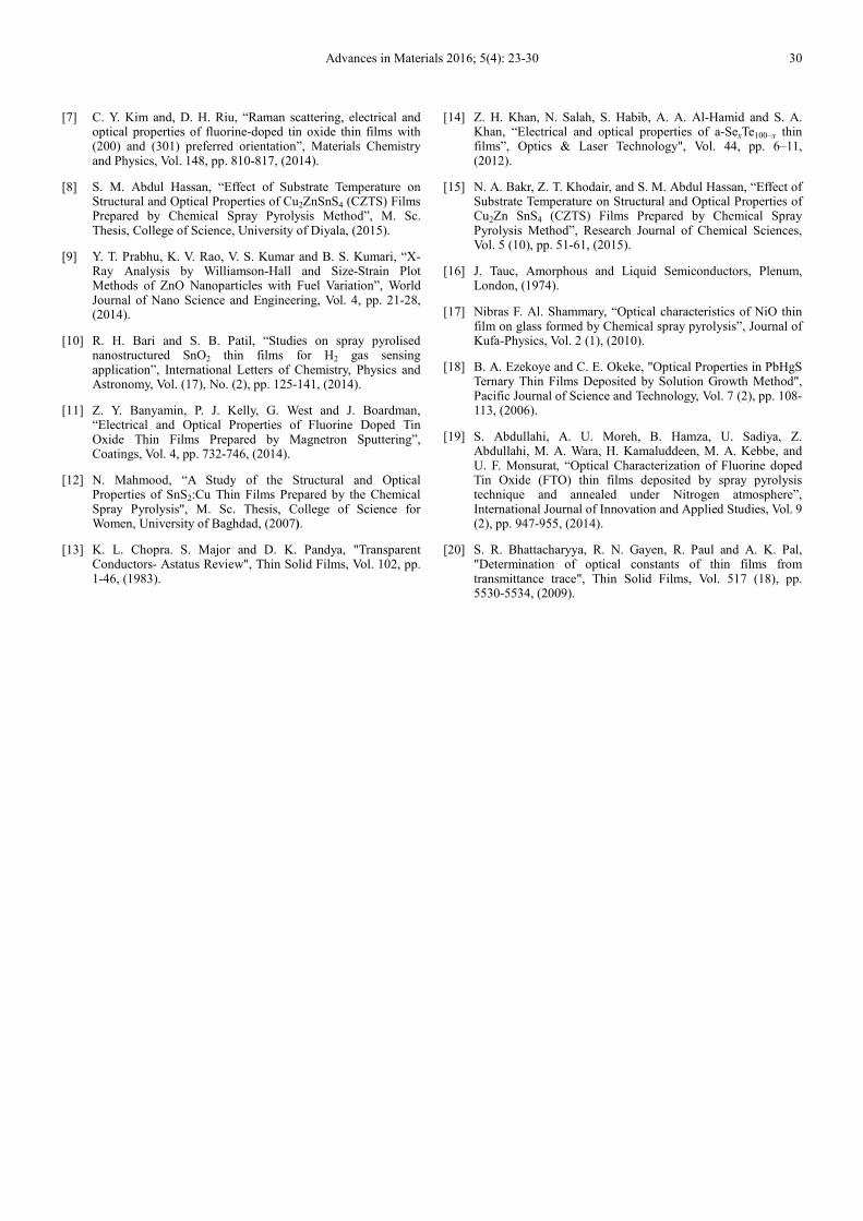
The width of the localized states available in the optical band gap of the films affects the optical band gap structure and optical transitions and it is called as Urbach tail, which is related directly to a similar exponential tail for the density of states of either one of the two band edges. The Urbach tail of the films can be determined by the following relation [17]:
α = αo exp (hν/Eu) (7)
Where hν is the photon energy, αo is constant, and Eu is the Urbach energy which refers to the width of the exponential absorption edge. Figure (10) shows the variation of (lnα) versus photon energy for the films. The obtained EU values are given in Table (4).
Fig. 10. Urbach Energies of the undoped and F-doped SnO2 films.
Table 3. Values of optical energy gap of the undoped and F-doped SnO2
films.
Sample Eg (eV)
undoped SnO2 3.79 SnO1.98F0.02 3.82 SnO1.96F0.04 3.83 SnO1.94F0.06 3.77 SnO1.92F0.08 3.72
Table 4. Urbach Energies of the undoped and F-doped SnO2 films.
Sample Eu (meV)
Undoped SnO2 747.88 SnO1.98F0.02 640.59 SnO1.96F0.04 625.91 SnO1.94F0.06 717.6 SnO1.92F0.08 776.69
The refractive index (no) can be determined from the reflectance (R) by using the relation [18]:
�� = ����������� ���� � 1�!� �⁄ � ���
��� (8)
Figure (11) shows the variation of the refractive index with the photon energy of the (SnO2-xFx) films (x = 0, 0.02, 0.04, 0.06 and 0.08). It is clear from this figure that the refractive index of these films slightly increases with increasing the doping percentage.
The extinction coefficient (ko) can be determined by using the relation [19]:
4
o
k αλ π= (9)
Where (λ) is the wavelength of the incident photon.
Fig. 11. Refractive index of the undoped and F-doped SnO2 films.
Figure (12) shows the variation in extinction coefficient as a function of the photon energy of the (F: SnO2) films with different doping percentage. It can be noticed that the extinction coefficient increases as the doping percentage increasing. This is attributed to the increases in absorption coefficient as the doping percentage increasing.
Fig. 12. Extinction coefficient of the undoped and F-doped SnO2 films.
29 Nabeel A. Bakr et al.: Effect of Fluorine Doping on Structural and Optical Properties of SnO2 Thin Films Prepared by Chemical Spray Pyrolysis Method
The variation of the real (ɛ1) and imaginary (ɛ2) parts of dielectric constant values versus photon energy of (SnO2-xFx) films with different doping percentage are shown in figures (13) and (14) respectively. The behavior of real part of dielectric constant is similar to that of refractive index because of the smaller value of (ko
2) compared with (no2) [20]:
2 2
1 o o
ε n k= − (10)
However, the imaginary part of dielectric constant is mainly depends on the extinction coefficient, which is related to the variation of absorption coefficient [20]:
2 2
2 o o
ε n k= (11)
It is found that the real and imaginary parts of dielectric constant increases with increasing of doping percentage.
Fig. 13. Real part of the dielectric constant of the undoped and F-doped
SnO2 films.
Fig. 14. Imaginary part of the dielectric constant of the undoped and F-
doped SnO2 films.
3.4. Conclusions
Thin films of SnO2-xFx, where x = 0, 0.02, 0.04, 0.06 and 0.08 have been successfully synthesized by chemical spray
pyrolysis technique. The Influence of doping on structural and morphological properties of these films was investigated. The XRD results showed that all films are polycrystalline in nature with tetragonal structure and preferred orientation along (110) plane. The intensity of peaks, the crystallite size and lattice constants decreased with increasing of doping. The decrease in average crystallite size shows that at least a small quantity of F ions substituted the O ions. The microstrain in the films is induced during the growth of thin films by varying displacements of the atoms with respect to their reference lattice position. All values of microstrain were positive which indicates the occurrence of tensile stress in the lattice. AFM results showed that the average grain size, average roughness and root mean square (RMS) decreased with increasing of doping. These results were qualitatively in agreement with the results of crystallite size obtained by XRD results. The result of optical measurements showed that transmittance of the (SnO2-xFx) films decreases with increasing the doping percentage and absorbance increased with increasing doping percentage. This is due to the formation of new localized levels which are capable to receive electrons and generate localized energy tails inside the optical energy gap which work on the absorption of low energy photons. The results showed that the optical energy gap for allowed direct electronic transition increases with increasing doping percentage to reach its maximum value of 3.83 eV at 0.04 doping percentage then it starts to fall down as the doping percentage increases further. The detailed study the effect of doping percentage on the optical properties has shown that all the optical properties such as absorption coefficient, refractive index, extinction coefficient and real and imaginary parts of dielectric constant have been affected by increasing the doping percentage.
References
[1] S. C. Ray, M. K. Karanjai and D. Dasgupta, "Tin dioxide based transparent semiconducting films deposited by the dip-coating technique", Surface and Coatings Technol., Vol. 102 (1), pp. 73-80, (1989).
[2] M. Batzill and U. Diebold, "The surface and Materials science of tin oxide", progress in surface science, Vol. 79, pp. 147-154, (2005).
[3] A. J. Freeman, K. R. Poeppelmeier, T. O. Mason, R. P. H. Chang and T. J. Marks, “Chemical and thin-film strategies for new transparent conducting oxides", MRS Bul, Vol. 25, pp. 45-51, (2000).
[4] J. E. House and K. A. House, Descriptive Inorganic Chemistry, Illinois Wesleyan University, Bloomington, Illinois, (2010).
[5] R. C. Weast and M. J. Astle, Hand book of Chemistry and physics, CRC press, (1979).
[6] A. Benhaoua, A. Rahal, B. Benhaoua, and M. Jlassi, “Effect of fluorine doping on the structural, optical and electrical properties of SnO2 thin films prepared by spray ultrasonic”, Superlattices and Microstructures, Vol. 70, pp. 61-69, (2014).
Advances in Materials 2016; 5(4): 23-30 30
[7] C. Y. Kim and, D. H. Riu, “Raman scattering, electrical and optical properties of fluorine-doped tin oxide thin films with (200) and (301) preferred orientation”, Materials Chemistry and Physics, Vol. 148, pp. 810-817, (2014).
[8] S. M. Abdul Hassan, “Effect of Substrate Temperature on Structural and Optical Properties of Cu2ZnSnS4 (CZTS) Films Prepared by Chemical Spray Pyrolysis Method”, M. Sc. Thesis, College of Science, University of Diyala, (2015).
[9] Y. T. Prabhu, K. V. Rao, V. S. Kumar and B. S. Kumari, “X-Ray Analysis by Williamson-Hall and Size-Strain Plot Methods of ZnO Nanoparticles with Fuel Variation”, World Journal of Nano Science and Engineering, Vol. 4, pp. 21-28, (2014).
[10] R. H. Bari and S. B. Patil, “Studies on spray pyrolised nanostructured SnO2 thin films for H2 gas sensing application”, International Letters of Chemistry, Physics and Astronomy, Vol. (17), No. (2), pp. 125-141, (2014).
[11] Z. Y. Banyamin, P. J. Kelly, G. West and J. Boardman, “Electrical and Optical Properties of Fluorine Doped Tin Oxide Thin Films Prepared by Magnetron Sputtering”, Coatings, Vol. 4, pp. 732-746, (2014).
[12] N. Mahmood, “A Study of the Structural and Optical Properties of SnS2:Cu Thin Films Prepared by the Chemical Spray Pyrolysis", M. Sc. Thesis, College of Science for Women, University of Baghdad, (2007).
[13] K. L. Chopra. S. Major and D. K. Pandya, "Transparent Conductors- Astatus Review", Thin Solid Films, Vol. 102, pp. 1-46, (1983).
[14] Z. H. Khan, N. Salah, S. Habib, A. A. Al-Hamid and S. A. Khan, “Electrical and optical properties of a-SexTe100–x thin films”, Optics & Laser Technology", Vol. 44, pp. 6–11, (2012).
[15] N. A. Bakr, Z. T. Khodair, and S. M. Abdul Hassan, “Effect of Substrate Temperature on Structural and Optical Properties of Cu2Zn SnS4 (CZTS) Films Prepared by Chemical Spray Pyrolysis Method”, Research Journal of Chemical Sciences, Vol. 5 (10), pp. 51-61, (2015).
[16] J. Tauc, Amorphous and Liquid Semiconductors, Plenum, London, (1974).
[17] Nibras F. Al. Shammary, “Optical characteristics of NiO thin film on glass formed by Chemical spray pyrolysis”, Journal of Kufa-Physics, Vol. 2 (1), (2010).
[18] B. A. Ezekoye and C. E. Okeke, "Optical Properties in PbHgS Ternary Thin Films Deposited by Solution Growth Method", Pacific Journal of Science and Technology, Vol. 7 (2), pp. 108-113, (2006).
[19] S. Abdullahi, A. U. Moreh, B. Hamza, U. Sadiya, Z. Abdullahi, M. A. Wara, H. Kamaluddeen, M. A. Kebbe, and U. F. Monsurat, “Optical Characterization of Fluorine doped Tin Oxide (FTO) thin films deposited by spray pyrolysis technique and annealed under Nitrogen atmosphere”, International Journal of Innovation and Applied Studies, Vol. 9 (2), pp. 947-955, (2014).
[20] S. R. Bhattacharyya, R. N. Gayen, R. Paul and A. K. Pal, "Determination of optical constants of thin films from transmittance trace", Thin Solid Films, Vol. 517 (18), pp. 5530-5534, (2009).