Embed Size (px)
Citation preview

Rev 0.1 10/13 Copyright © 2013 by Silicon Laboratories AN794
AN794
C8051F850 BLDC REFERENCE DESIGN KIT
1. Introduction
This design kit provides a complete system-level solution for sensorless, brushless dc (BLDC) motors. Thisapplication note includes complete schematics, PCB layouts and firmware.
This kit supports 3-phase BLDC motors that meet the following specifications:
Trapezoidal back-EMF
Max operating voltage of between 10 V to 24 V dc
24 kHz PWM frequency
Maximum average current of 10 A
Maximum speed not exceeding 200,000 rpm for a 2-pole BLDC motor
Overcurrent detection capability stops the motor when average current exceeds 10 A.
Motor Stall detect capability stops the motor when a motor stall is detected or extreme loads encountered.
Tachometer Frequency Generator (FG) output signal
The kit aims to demonstrate the capabilities of the C8051F850 for operating BLDC motors. The unique featuresoffered by this MCU for BLDC motor operation are:
PWM synchronized blanking of comparator for BEMF Zero-Crossing Detection
Automatic PWM duty cycle reduction to limit motor current during startup
Hyperdrive mode to increase the maximum speed of some motors
1.1. Kit ContentsThe kit consists of the following:
One MCU Board: MCRD-MCU-C8051F850 with the motor control firmware preprogrammed into the MCU
One Powertrain Board: MCRD-PWR-NLV-F85X
One BLDC Motor: Turnigy 450 Series 3800 kV Brushless Outrunner Helicopter Motor
One Motor Mount Board
One 8-bit MCU Kit CD
One 12 V, 5 Amp Universal Input Power Adapter

AN794
2 Rev 0.1
1.2. Operational Specifications
The kit uses the Turnigy 450 Series 3800 kV Brushless Outrunner Helicopter Motor.The motor operating range and specifications are given in Table 1.
The operating ranges of the hardware and firmware in the kit are shown in Table 2.
In the default operation mode using the ac/dc adapter, the operating parameters of the motor are shown in Table 3.
Table 1. Motor Specifications
Parameter Min Typ Max Unit
Number of poles — 6 —
Operating voltage 7.4 — 14.8 V
Maximum current — — 35 A
Maximum power — — 365 W
No-load full-speed average current @ 12 V — 3.66 — A
No-load peak startup current @ 12 V — — 11 A
Motor constant — 3800 — RPM/V
Maximum speed @ 12 V — — 45600 RPM
Weight — 80 — g
Table 2. Hardware and Firmware Operating Range
Parameter Min Typ Max Unit
Power supply 10 — 24 V
Motor driver PWM frequency — 24 — kHz
Continuous average output current — — 10 A
Speed range (2-pole motor) 2250 — 200000 RPM
Speed range (4-pole motor) 1125 — 100000 RPM
Speed range (6-pole motor) 750 — 66667 RPM
Table 3. Reference Design Kit Operating Specifications
Parameter Value Unit
Power supply 12 V
No-load full-speed average current @ 12 V 3.66 A
No-load peak startup current @ 12 V 11 A
Maximum speed @ 12 V 45600 RPM
Motor driver PWM frequency 24 kHz
Maximum Power 43.92 W

AN794
Rev 0.1 3
2. Theory of Operation
This section describes the theory of operation of 3-phase BLDC motors so that users of this design kit canunderstand the design choices they may face in their application.
2.1. System ModelFirstly, we will describe the system model of 3-phase BLDC motor including its drive system. This will help usunderstand the behavior of the system and design the appropriate drive systems and filters for our application.
Figure 1. System Model of 3-Phase BLDC Motor Drive
R
L
eB
B
R
L
eA
A
R
L
eC
C
Rx
Vdc
AH
AL
BH
BL
CH
CL
N
IB
IC
IA

AN794
4 Rev 0.1
A BLDC motor has 3 stator windings and is driven by an inverter circuit that consists of 6 switches. Figure 1 showsthe equivalent circuit of a Y-connection BLDC motor and the inverter circuit topology. In this model, the statorinductance and resistance of each phase are assumed to be equal. RX is a very small valued resistor used forcurrent measurement and can be assumed to be zero to simplify the analysis of the different modes of operation.
The electrical equations of the system model can be expressed by the following equation:
The electromagnetic torque is described by the following equation:
VA VN– IAR LdIAdt
-------- eA (1)
VB VN– IBR LdIBdt-------- eB (2)
VC VN– ICR LdICdt
-------- eC (3)
eA KmFe (4)
eB KmF e23
------– (5)
eC KmF e43
------– (6)
m2
Np-------
de
dt---------= (7)
=
=
=
+ +=
+ +=
+ +=
Where:
VA VB VC denote the voltages of motor terminals A, B, and C, respectively
IA IB IC denote the phase currents entering terminals A, B, and C, respectively
eA eB eC denote the phase back-EMF (BEMF) associated with terminals A, B, and C, respectively
R is the stator phase resistance
L is the stator phase inductance
VN is the neutral voltage of the Y connection
K is the motor constant
NP is the number of poles in the motor
e is the electrical angle of the motor
m is the angular speed of the motor
F e represents the BEMF reference wafeform as a function of rotor electrical angle
Te KIAF e KIBF e23
------– KICF e
43
------– (8)+ +=
AN794
Rev 0.1 5
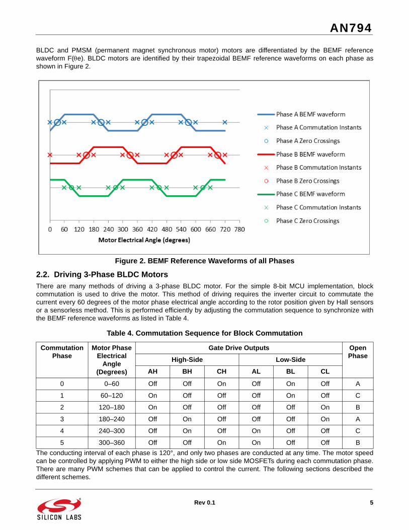
BLDC and PMSM (permanent magnet synchronous motor) motors are differentiated by the BEMF referencewaveform F(e). BLDC motors are identified by their trapezoidal BEMF reference waveforms on each phase asshown in Figure 2.
Figure 2. BEMF Reference Waveforms of all Phases
2.2. Driving 3-Phase BLDC MotorsThere are many methods of driving a 3-phase BLDC motor. For the simple 8-bit MCU implementation, blockcommutation is used to drive the motor. This method of driving requires the inverter circuit to commutate thecurrent every 60 degrees of the motor phase electrical angle according to the rotor position given by Hall sensorsor a sensorless method. This is performed efficiently by adjusting the commutation sequence to synchronize withthe BEMF reference waveforms as listed in Table 4.
The conducting interval of each phase is 120°, and only two phases are conducted at any time. The motor speedcan be controlled by applying PWM to either the high side or low side MOSFETs during each commutation phase.There are many PWM schemes that can be applied to control the current. The following sections described thedifferent schemes.
Table 4. Commutation Sequence for Block Commutation
Commutation Phase
Motor Phase Electrical
Angle (Degrees)
Gate Drive Outputs Open Phase
High-Side Low-Side
AH BH CH AL BL CL
0 0–60 Off Off On Off On Off A
1 60–120 On Off Off Off On Off C
2 120–180 On Off Off Off Off On B
3 180–240 Off On Off Off Off On A
4 240–300 Off On Off On Off Off C
5 300–360 Off Off On On Off Off B

AN794
6 Rev 0.1
2.2.1. High-Side PWM
Figure 3. High-Side PWM Scheme
High-side PWM can be used if the high-side MOSFETs are N-channel enhancement type MOSFETs. It is notadvisable to apply this scheme to P-channel MOSFETs because they are typically slower than N-channelMOSFETs. The advantage of high-side PWM scheme is that it is simple to implement since it requires only 1 PWMsignal to be active at any time. Another advantage is that the bootstrap capacitor of a typical high-side driver of anN-channel MOSFET is guaranteed to get enough charge when its low-side MOSFET is enabled. The disadvantageof this scheme is heat built-up by re-circulation current through the body diodes of the low-side MOSFETs duringthe PWM off cycle can cause problems if these MOSFETs cannot dissipate the heat. The sequence of current flowthrough the inverter circuit is illustrated in Figures 4, 5, and 6.

AN794
Rev 0.1 7
Figure 4. Current Flow: High-Side PWM, PWM On Cycle
R
L
eB
B
R
L
eA
A
R
L
eC
C
Rx
Vdc
AH
AL
BH
BL
CH
CL
N
IC

AN794
8 Rev 0.1
Figure 5. Current Flow: High-Side PWM, Start (Part 1) of PWM Off Cycle
At the start of the PWM off cycle, current can flow in the open terminal. This effect will be explained in the nextsection. When the low level current in the open terminal decays to zero, only the recirculation current remainsflowing as shown in Figure 6.
R
L
eB
B
R
L
eA
A
R
L
eC
C
Rx
Vdc
AH
AL
BH
BL
CH
CL
N
IC
VAe
IC

AN794
Rev 0.1 9
Figure 6. Current Flow: High-Side PWM, (Part 2) of PWM Off Cycle
If the PWM off cycle is sufficiently long, the remaining recirculation current will decay to zero. The oscilloscopecapture in Figure 7 shows the voltage of an open terminal for all the phases of the PWM off cycle:
R
L
eB
B
R
L
eA
A
R
L
eC
C
Rx
Vdc
AH
AL
BH
BL
CH
CL
N
IC
VAe

AN794
10 Rev 0.1
Figure 7. Oscilloscope Capture of Open Terminal
Note the slight dip in voltage during “PWM Off phase Part 2”. This corresponds to the period when a small currentflows in the open terminal.
2.2.2. Low-Side PWM
Figure 8. Low-Side PWM Scheme
Low-side PWM is typically used in low-cost designs where the high-side MOSFETs are P-channel type MOSFETswith simple discrete drivers where high-side PWM would not be suitable. As in the high-side PWM scheme, low-side PWM is simple to implement as it requires only one PWM signal to be active at any time. Like the high-sidePWM, the disadvantage is the potential heat problems due to the recirculation current.
AN794
Rev 0.1 11
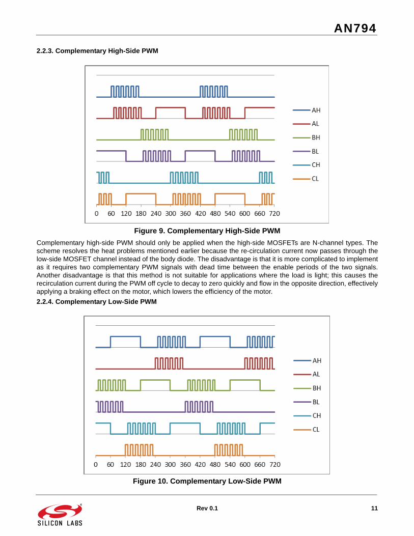
2.2.3. Complementary High-Side PWM
Figure 9. Complementary High-Side PWM
Complementary high-side PWM should only be applied when the high-side MOSFETs are N-channel types. Thescheme resolves the heat problems mentioned earlier because the re-circulation current now passes through thelow-side MOSFET channel instead of the body diode. The disadvantage is that it is more complicated to implementas it requires two complementary PWM signals with dead time between the enable periods of the two signals.Another disadvantage is that this method is not suitable for applications where the load is light; this causes therecirculation current during the PWM off cycle to decay to zero quickly and flow in the opposite direction, effectivelyapplying a braking effect on the motor, which lowers the efficiency of the motor.
2.2.4. Complementary Low-Side PWM
Figure 10. Complementary Low-Side PWM

AN794
12 Rev 0.1
Complementary low-side PWM should only be applied when the high-side MOSFETs are N-channel type. It hassimilar advantages and disadvantages as complementary high-side PWM.
2.2.5. Mixed Mode PWM
Figure 11. Mixed Mode PWM
Mixed mode PWM is a combination of high-side and low-side PWM. Mixed mode PWM is simple to implementbecause it requires only 1 active PWM signal at any time. But it can normally be applied only if all the powerMOSFETs are N-channel type. The advantage of mixed mode PWM over either high-side or low-side only PWM isthat the re-circulation current load is shared between the body diodes of all the 6 MOSFETs. In high-side or low-side PWM schemes, the re-circulation current load is shared between the body diodes of 3 MOSFETs. Hence,mixed mode PWM offers improved long term reliability compared to high-side only or low-side only PWM schemes.
AN794
Rev 0.1 13
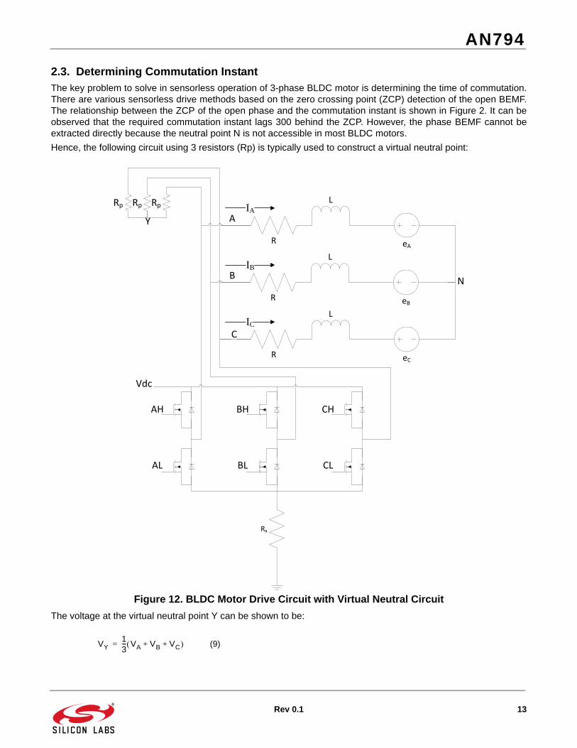
2.3. Determining Commutation InstantThe key problem to solve in sensorless operation of 3-phase BLDC motor is determining the time of commutation.There are various sensorless drive methods based on the zero crossing point (ZCP) detection of the open BEMF.The relationship between the ZCP of the open phase and the commutation instant is shown in Figure 2. It can beobserved that the required commutation instant lags 300 behind the ZCP. However, the phase BEMF cannot beextracted directly because the neutral point N is not accessible in most BLDC motors.
Hence, the following circuit using 3 resistors (Rp) is typically used to construct a virtual neutral point:
Figure 12. BLDC Motor Drive Circuit with Virtual Neutral Circuit
The voltage at the virtual neutral point Y can be shown to be:
R
L
eB
B
R
L
eA
A
R
L
eC
C
Rx
Vdc
AH
AL
BH
BL
CH
CL
N
Rp Rp Rp
Y
IB
IC
IA
VY13--- VA VB VC+ + (9)=

AN794
14 Rev 0.1
During the commutation phase 1 (0° to 60°), phases C and B are conducting; the phase current and voltagerelationships can be easily expressed as follows:
Substituting (10) to (12) into (2) and (3), we can derive the following expression for the neutral voltage:
Substituting (13) and (14) into (9), we derive the virtual neutral voltage:
From (14) and (15), it can be observed that a comparator can be used to compare voltages at A and Y to detect theZCP of the BEMF of A:
It is important to note that the above equations hold irrespective of whether PWM drive is applied to the high side orlow side MOSFET. Hence, ZCP occurs when VY – VA crosses zero, and a scheme based on comparing thevoltages between Y and A will yield the zero crossing.
IC IB (10)IA 0 (11)eC eB (12)VA eA VN (13)+=
–==
–=
VN12--- VB VC+ (14)=
VY13---eA VN+ (15)=
VY VA–23---– eA (16)=

AN794
Rev 0.1 15
2.3.1. High-Side PWM (Part 1 of PWM Off Cycle)
In the earlier analysis, the assumption was made that the open phase A was not conducting during commutationphase 1. But this is not true during the initial phase of the PWM off cycle. During the PWM off phase (assuminghigh-side PWM), majority of the current flow is as shown below:
Figure 13. Commutation Phase 1: High-Side PWM Off Majority Current Flow
If we assume the forward bias voltage of the body diode of the CL MOSFET is VFCL, then during the start of the offphase:
Substituting (17) and (18) into (14), the neutral point voltage is:
R
L
eB
B
R
L
eA
A
R
L
eC
C
Rx
Vdc
AH
AL
BH
BL
CH
CL
N
IC
Rp Rp Rp
Y
VAe
VC VFCL– (17)
VB 0 (18)=
=
VN
VFCL–
2----------------- (19) =

AN794
16 Rev 0.1
The voltage after the BEMF element in the system model (refer to Figure 15), VAe, is:
If the minimum forward diode voltage required for current to flow is VFmin, then current will flow in the open phaseif the following condition is met:
The current flow is illustrated in Figure 14 and also earlier in Figure 5.
Figure 14. High-Side PWM: PWM Off with Current Flow in Open Terminal
VAe VN eA+ eA
VFCL
2------------- (20)–= =
VAe VFmin
eA
VFCL
2------------- VFmin (21)–
–
R
L
eB
B
R
L
eA
A
R
L
eC
C
Rx
Vdc
AH
AL
BH
BL
CH
CL
N
IC
Rp Rp Rp
Y
VAe
IC

AN794
Rev 0.1 17
During the commutation Phase 1, when the BEMF of phase A is rising and ZCP of A has not yet occurred, theBEMF of phase A (eA) is negative (see 0° to 30° in Figure 2); so, it is possible for the condition of inequality (21) tobe met. When this occurs, the actual terminal voltage of A when the body diode of AL conducts is:
And the virtual neutral voltage can be derived from (9), (17), (18), and (22):
When PWM is off and current flows in the open terminal, the comparison relationship is:
This small-value current flowing in the open terminal may or may not decay to zero before the PWM returns to thePWM on cycle. Hence, when current flows in the open terminal, it is impossible to measure the zero-crossing point.And this problem can be further exacerbated by parasitic capacitance across the drain-source terminals of thepower MOSFETs that can cause ringing at the motor terminals.
2.3.2. High-Side PWM (Part 2 of PWM Off Cycle)
When the current in the open terminal decays to zero, only the re-circulation current flows through the circuit alongthe path illustrated in Figure 13. The voltages at terminals A and Y are simply:
The comparison relationship is still the same as when PWM is on:
VA VFAL– VFmin (22)–=
VY13---– VFAL VFCL+ (23)=
VY VA–13---– 2– VFAL VFCL+ (24)=
VA VAe eA
VFCL
2------------- (25)
VY13--- eA 3–
VFCL
2-------------
(26)=
–= =
VY VA–23---– eA (16)=
AN794
18 Rev 0.1
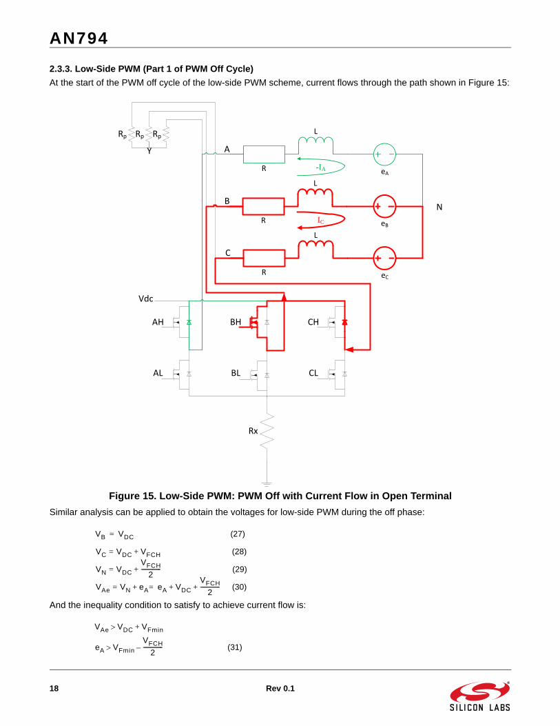
2.3.3. Low-Side PWM (Part 1 of PWM Off Cycle)
At the start of the PWM off cycle of the low-side PWM scheme, current flows through the path shown in Figure 15:
Figure 15. Low-Side PWM: PWM Off with Current Flow in Open Terminal
Similar analysis can be applied to obtain the voltages for low-side PWM during the off phase:
And the inequality condition to satisfy to achieve current flow is:
R
L
eB
B
R
L
eA
A
R
L
eC
C
Rx
Vdc
AH
AL
BH
BL
CH
CL
N
IC
Rp Rp Rp
Y
-IA
VB VDC (27)
VC VDC VFCH (28)
VN VDC
VFCH
2-------------- (29)
VAe VN eA eA VDC
VFCH
2-------------- (30)+ +=+=
+=
+=
=
VAe VDC VFmin
eA VFmin
VFCH
2-------------- (31)–
+

AN794
Rev 0.1 19
And the terminal voltages at A and Y are:
The corresponding comparison relationship is:
2.3.4. Low-Side PWM (Part 2 of PWM Off Cycle)
When the open terminal current decays to zero, the voltages at terminals A and Y are simply:
The comparison relationship is still the same as when PWM is on:
2.3.5. Summary of Terminal Voltage Comparisons for ZCP Detection
Table 5 presents a summary of the terminal voltage comparison with the virtual neutral point voltage:
These equations will aid in the selection of the hardware design, PWM scheme, and firmware algorithm to be usedin the design kit.
Table 5. Terminal Voltage Comparison Equations
Active PWM State VY-VA Equation
PWM on
High-side/Low-side PWM off, zero current flows in open terminal A
High-side PWM off, non-zero current flows in open terminal A conditional upon:
Low-side PWM off, non-zero current flows in open terminal A conditional upon:
VA VDC VFAH (32)
VY VDC13--- VFAH VFCH+ (33)+=
+=
VY VA–13--- 2– VFAH VFCH+ (34)=
VA VAe eA VDC
VFCH
2-------------- (35)
VY VDC13--- eA 3+
VFCH
2--------------
(36)+=
+ += =
VY VA–23---– eA (16)=
VY VA–23---– eA (16)=
VY VA–23---– eA (16)=
VY VA–13---– 2– VFAL VFCL+ (24)=
eA
VFCL
2------------- VFmin (21)–
VY VA–13--- 2– VFAH VFCH+ (34)=
eA VFmin
VFCH
2-------------- (31)–

AN794
20 Rev 0.1
3. System Implementation
This section describes the system implementation of the design kit. Schematics for the design kit can be found in"8. Schematics" on page 57. The kit consists of two boards: an MCU board and a powertrain board. The blockdiagram of the reference design is shown in Figure 16.
Figure 16. Reference Design Block Diagram
3.1. Powertrain BoardThe powertrain board is designed to meet the following key motor specifications:
Motor supply voltage range of 10 to 24 V
Maximum average current of 10 amps
It consists of the following components that are relevant to this application:
6 IRFH7446 Power MOSFETS for the inverter circuit
3 Silicon Labs Si8230 isolated dual drivers
An LDO to generate the 3.3 V required by the MCU board
50 m current sensing resistor rated for 10 W
Motor terminal blocks to allow user to attach their own motor
Resistor divider to generate attenuated motor voltage supply (VMDC) - allows MCU to determine if motor supply voltage is high enough for safe operation
Resistor dividers to generate attenuated motor phase voltages with a small positive offset voltage (VMA, VMB, VMC)
Resistor network to generate attenuated sum of motor phase voltages with a small positive offset voltage (VMY)
Rx
MTR_VDC
AH
AL
BH
BL
CH
CL
Three‐Phase Inverter
J6
MTR_VA
MTR_VB
MTR_VC
M
J5
MTR_VDC
12V
5V
3.3V
Regulators
+12V
+3.3V
+5V
MCU_GND
VMA
MTR_VA
R23
R27C10
+3.3V
R68
MCU_GND
MTR_VA
MTR_VB
MTR_VC
C14 R34 R36
R33
R31
R35
R32
+3.3V
R73R72 R74
Zero‐Crossing Detect Filter Circuit
MTR_VA
MTR_VB
MTR_VC
+3.3V
VMA
VMB
VMC
VMY
IM_0P
Gate Driver
Motor Mount BoardMCRD‐MMT‐1525
Powertrain BoardMCRD‐PWR‐NLV
+
‐
+
‐
C8051F850
VMYVMCVMBVMA
Current sense amplifier
POT
+3.3V
Start/Stop
Direction
FG
UART_RX
UART_TX
UART‐USB Bridge
C2 USB Debug
USB Hub
USB Interfaces
UART_TX
UART_RX
USB of PC
+3.3V
MCU BoardMCRD‐MCU‐C8051F850

AN794
Rev 0.1 21
3.1.1. Attenuated Motor Voltage Circuit
There is a circuit to provide an attenuated motor voltage signal to the MCU as shown below:
Figure 17. Attenuated Motor Voltage Circuit
This circuit allows the MCU to measure the motor voltage and determine whether the voltage is high enough tooperate the motor.
3.1.2. Back-EMF Filter Circuit
The BEMF filter circuit is intended to attenuate the motor terminal voltage to a level that can be used by the MCU.The circuit for one of the terminals is shown below:
Figure 18. Back-EMF Filter Circuit for Motor Terminal Voltage
A slight positive offset voltage via the pull-up R68 because the voltage at MTR_VA may be negative during thePWM off cycle (refer to equations 22 and 25) of high-side PWM operation. It can be shown that the voltage at VMAis:
This sets the offset voltage at 0.55 V and the gain at 0.0877. C10 is a 100 pF capacitor that filters sharp ringingvoltages at the motor terminal.
MCU_GND
MTR_VDC
VMDC
R301.15K
C13
100pF
R269.76K
MCU_GND
VMA
MTR_VA
R239.76K
R271.15K
C10
100pF
+3.3V
R685.1K
VVMA
3.3R68-----------
1R23----------- 1
R27----------- 1
R68-----------+ +
-----------------------------------------------
VMTR_VA
R23-----------------------
1R23----------- 1
R27----------- 1
R68-----------+ +
----------------------------------------------- (37)+=

AN794
22 Rev 0.1
3.1.3. Virtual Neutral Filter Circuit
The virtual neutral voltage is also adjusted similarly with a resistor network:
Figure 19. Virtual Neutral Filter Circuit
It can be similarly demonstrated that the voltage at VMY is:
Recall equation 9:
This shows that the voltage at VMY is the virtual neutral voltage with the same scale and offset applied in the samemanner as VMA. Thus, the VMx signals from the resistor network circuits can be used for back-EMF zero crossingdetection by the MCU’s comparator without saturating. C14 is a 100 pF capacitor that filters sharp ringing voltagesat the motor terminals.
3.2. MCU BoardThe MCU board consists of the following:
C8051F850-A-GU QSOP-24 package
2 push-buttons
3 controllable LEDs
1 rotary variable resistance potentiometer
Op-amp to amplify and bias the current sense voltage
USB Hub to support:C2 USB debug interfaceCP2103 USB-UART bridge operating at 115200 baudCP2112 USB-I2C bridge
Configurable jumpers to select either Hall-sensored or sensorless mode of operation
Test points for connecting to gate drive of user powertrain board and motor.
The crossbar is configured such that all digital pins have pull-ups disabled. This is an unusual configuration of thedigital pins, which will be explained in "3.3. Back-EMF Zero Crossing Point Detection Technique" on page 25.
MCU_GND
MTR_VA
MTR_VB
MTR_VC
C14
100pF
R34
1.15K
R36
1.15K
R33 9.76K
R31 9.76K
R35
1.15K
R32 9.76K
+3.3V
R735.1K
R725.1K
R745.1K
VVMY
+3.3R72-----------
1R31----------- 1
R34----------- 1
R72-----------+ +
-----------------------------------------------
VMTR_VA VMTR_VB VMTR_VC+ + 3 R31
---------------------------------------------------------------------------------------
1R31----------- 1
R34----------- 1
R72-----------+ +
--------------------------------------------------------------------------------------- (38)+=
VY13--- VA VB VC+ + (9)=

AN794
Rev 0.1 23
3.2.1. Gate Drive Pin Connections
Pins P1.2 to P1.7 are connected to the gate drive pins of the powertrain board. These pins are configured as push-pull outputs by the firmware. The pin connections, pin names and associated motor phase are specified in Table 6.
This sequence facilitates the commutation using the crossbar pin skip register P1SKIP. For example in thecommutation sequence shown in Figure 20:
Figure 20. Commutation from PWM0A to PWM1A
Prior to the commutation event, P1SKIP contains the value 0xF7. The commutation event can be easily executedby a single C language instruction:
P1SKIP = 0xDF; // P1.5 can be assigned by crossbar
Depending on the firmware configuration, users can observe PWM signals on either the high-side or low-side gatedrive pins.
3.2.2. Motor Sensor Connections
Pins P0.0, P0.1 and P0.2 are connected to jumpers J110, J111, J112 respectively. The jumpers allow the user toselect either Hall-sensored mode operation or sensorless mode operation. For sensorless mode operation, theMCU expects these pins to be connected to attenuated motor phase voltages that are offset with a small positivevoltage (see "3.1.2. Back-EMF Filter Circuit" on page 21). In sensorless mode operation, P0.3 must be connectedto the attenuated virtual neutral that is offset with a small positive voltage. Refer to the attenuation and offset circuitin "3.1.3. Virtual Neutral Filter Circuit" on page 22. As explained earlier sections, the offset voltage is requiredbecause the voltage at the motor terminal may be negative during the PWM off cycle when PWM is applied to ahigh-side FET.
Table 6. MCU Motor Gate Drive Pin Connection
MCU Pin Connection Name Controlled Motor Phase
P1.2 PWM0B_GD0_EN A
P1.3 PWM0A A
P1.4 PWM1B_GD1_EN B
P1.5 PWM1A B
P1.6 PWM2B_GD2_EN C
P1.7 PWM2A C

AN794
24 Rev 0.1
3.2.3. Current Sensing Circuit
Pin P0.6 is connected to the current sensing voltage of the motor drive circuit. Jumper 113 allows the user to select1 of 2 options to measure this voltage:
Direct connection to low-side current sensing resistor. This is a low-cost option when the user is only concerned with over-current protection and hence is only required to detect high current on this pin.
Output of a op-amp circuit (refer to U201 in schematics). This is the default jumper selection. This option is for applications that need to measure small current for motor start-up.
Figure 21. Current Sensing Opamp Gain Circuit
The current sense circuit adds a small 0.275V offset and gain of 1.545 for the current sense voltage.
Gain = 1.55
Vbias = 0.275V
+
-
3
21U201-A
LMV842MM/NOPB
+
-
5
67
4
8
U201-B
LMV842MM/NOPB
R208
3.3K
R209
3.3K
R2055.1K
R207
5.1K
R20210K
R203910
C202NI
C203
NI
C2040.1uF
J20
2D
O N
OT
IN
ST
ALL
R201NI
J20
1D
O N
OT
IN
ST
ALL
R204NI
R206
NI
J203
DO NOT INSTALL
C2010.1uF
GND
+ 3.3V
+ 3.3V
GND
IM_0N
IM_0P
I _MEAS
GND
GND

AN794
Rev 0.1 25
3.3. Back-EMF Zero Crossing Point Detection TechniqueDetecting the Back-EMF zero crossing point can be challenging when there is an active PWM signal that interfereswith the BEMF signal. Some designs implement a low-pass filter for the terminal signals and the virtual neutral.However, a low-pass filter is not suitable for motors with high commutation frequencies because of the phase shiftcaused by the filter.
This design kit implements a technique that takes advantage of some unique features of the C8051F850. Referringto the terminal comparison equations in Table 5 on page 19, it can be observed that the open terminal does notyield any zero crossing information when current flows through that terminal. So, a tracking signal is used todisable a comparator input so that the comparator is effectively not operational when current is flowing in the openterminal.
When BEMF is rising in the open terminal, the firmware configures the peripherals to operate as shown inFigure 22.
Figure 22. Peripheral Configuration for ZCP Detection on Rising BEMF Signal
When the BEMF is falling in the open terminal, the firmware re-configures the peripherals to operate as shown inFigure 23.
Figure 23. Peripheral Configuration for ZCP Detection of Falling BEMF Signal
+
‐
CMP0
VMA
VMY
P0.3 = PCA CEX0Operating as tracking signal
P0MDIN.3 = 1
Output = high before ZCP
+
‐
CMP0
VMA
VMY
P0.0 = PCA CEX0Operating as tracking signal
P0MDIN.0 = 1
Output = high before ZCP

AN794
26 Rev 0.1
Recall from Table 5 the terminal voltage comparison equations; they show that ZCP cannot be detected reliablywhen current is flowing in the open terminal because the voltages are dominated by the forward bias voltage of thebody diode of the power MOSFETs. Thus, a tracking signal is used to enable the comparator for use at appropriatetimes during the PWM cycle.
The tracking signal technique requires the following conditions to be met:
1. Ensuring the filtered terminal and virtual neutral voltages are positive - this is accomplished by adding a small positive offset voltage in the filter circuits as shown in Figure 18 on page 21 and Figure 19 on page 22.
2. MCU disables the pull-ups via the crossbar.
3. The pin that is connected to negative input of comparator is configured as digital input (P0MDIN.x = 1).
4. CEX0 is setup as a PWM tracking signal connected to the negative input of the comparator as shown in Figures 22 and 23.
When the motor PWM duty cycle is low (inactive period is much longer than the active period), CEX0 is setup tosynchronize with the motor PWM signal to observe the BEMF only at the tail end of the inactive part of the PWMcycle as shown in Figure 24:
Figure 24. Active High Motor PWM (Tracking Synchronization for Low Duty Cycle)
This corresponds to the last part of the motor PWM off cycle when no current flows in the open terminal, as shownin Figure 7 on page 10.
When the motor PWM duty cycle is high, CEX0 is setup to observe the BEMF at the tail end of the inactive part ofthe PWM cycle and the entire active part of the PWM cycle as shown in Figure 25.
Figure 25. Active High Motor PWM (Tracking Synchronization for High Duty Cycle)
The advantage of this technique is that blanking out the undesirable parts of the BEMF signal does not incur anyCPU overhead. If the tracking signal is not used, the MCU must be interrupted at least twice every PWM cycle toenable and disable the comparator to observe the BEMF. When this processing overhead is removed, a higherfrequency motor PWM signal can be applied. This leads to lower current ripple and reduced torque ripple duringthe operation of the BLDC motor.
CEX1 (motor PWM)
CEX0 (tracking signal) Comparator active tracking
PCA Cycle Overflow
CEX1 (motor PWM)
CEX0 (tracking signal) Comparator active tracking
PCA Cycle Overflow

AN794
Rev 0.1 27
3.4. PWM and Comparator Configuration SequencesBased on the different PWM techniques and Back-EMF ZCP detection techniques, we can derive the sequences ofperipheral assignments for different PWM modes. Tables 7, 8, and 9 specify the peripheral assignment sequencesfor the three different PWM modes in a specific direction.
For rotation in the opposing direction, the peripheral configuration sequences can be adjusted by exchanging theBEMF rows with the same “Open Phase” terminal.
Table 7. High-Side PWM Peripheral Configuration Sequence
State Gate Drive Outputs BEMF
High-Side Low-Side Open Phase
Slope CP0+ CP0- and
CEX0AH BH CH AL BL CL
0 PWM L L L H L C \ VMC VMY
1 L L PWM L H L A / VMY VMA
2 L L PWM H L L B \ VMB VMY
3 L PWM L H L L C / VMY VMC
4 L PWM L L L H A \ VMA VMY
5 PWM L L L L H B / VMY VMB
Table 8. Low-Side PWM Peripheral Configuration Sequence
State Gate Drive Outputs BEMF
High-Side Low-Side Open Phase
Slope CP0+ CP0- and
CEX0AH BH CH AL BL CL
0 H L L L PWM L C \ VMC VMY
1 L L H L PWM L A / VMY VMA
2 L L H PWM L L B \ VMB VMY
3 L H L PWM L L C / VMY VMC
4 L H L L L PWM A \ VMA VMY
5 H L L L L PWM B / VMY VMB
Table 9. Mixed Mode PWM Peripheral Configuration Sequence
State Gate Drive Outputs BEMF
High-side Low-side Open phase
Slope CP0+ CP0- and
CEX0AH BH CH AL BL CL
0 H L L L PWM L C \ VMC VMY
1 L L PWM L H L A / VMY VMA
2 L L H PWM L L B \ VMB VMY
3 L PWM L H L L C / VMY VMC
4 L H L L L PWM A \ VMA VMY
5 PWM L L L L H B / VMY VMB

AN794
28 Rev 0.1
3.5. BLDC Motor Startup TechniqueIn the typical BLDC motor sensorless starting phase, the motor is driven like a stepper motor. The motor is initiallycommutated very slowly then velocity is increased while the PWM duty cycle is increased to boost the appliedmotor voltage in an attempt to keep the current constant.
However, it is not easy to predetermine PWM duty cycle for constant current level because the motor load maychange or the motor supply voltage fluctuates. The design kit uses the comparator clear feature to trim the motorPWM duty cycle automatically to ensure that the current does not exceed a predetermined level regardless of themotor load or motor supply voltage. During motor startup, the comparator and PWM are configured as shown inFigure 26.
Figure 26. Comparator and PCA Configuration for Motor Startup
Using the comparator clear mechanism, the PWM signal is automatically shut off for that cycle when the currentsensing voltage exceeds 1.8 V. The firmware programs the MCU to generate a 50% duty cycle PWM signal formotor startup and lets the comparator clear functionality trim the duty cycle to limit the peak current. The currenttrip level can be adjusted by changing the resistors R208 and R209 shown in Figure 21 on page 24. The gain of theop-amp = R207/R209. R208 and R209 should always have the same value; R205 and R207 should always havethe same value. In the reference design kit, the limit is set such that the current sensing voltage will trigger thecomparator at twice the maximum current supported by the motor. The trigger limit is set at 20 A in the designbecause the average current will not exceed 10 A if the motor PWM is running at the maximum 50% duty cycle.Using this method, the firmware does not need to store a table of duty cycles to use during startup.
During startup, the firmware commutates at a rate such that the angular speed is increased at a constant rate. Ascommutation always drives the rotor a fixed angle, the angular speed is directly proportional to the reciprocal of thetime interval since the last commutation. At the same time, we also want the speed to be increased at a linear rate:
+
‐
CMP0
I_measOutput to be used by PCA Comparator Clear for CEX1
(Motor PWM)
Internal 1.8V
Motor PWM (CEX1) with comparator clearPCA0CLR.CPCE1 = 1
I_meas
1.8V

AN794
Rev 0.1 29
Figure 27. Motor Startup (Linearly Increasing Angular Speed)
Each Ti represents the time interval between successive commutation instants. It can be demonstrated that thetime interval can be represented by the following recurrence relationship:
The first 3 terms can be worked out off line and stored within the firmware using only 6 bytes of code memory.Using binomial expansion, the subsequent terms can be computed in firmware using the following approximation:
This method significantly reduces the amount of code space to store the startup interval table. The firmware willoperate in this startup mode until the motor speed reaches 5% of the maximum motor speed.
Rotor speed
TimeTk Tk+1
C/Tk‐1
C/Tk
C/Tk+1
Tk 1+12--- Ti
i 0=
k
14Tk
Ti
i 0=
k
--------------+ 1– (39)=
Tk 1+
Tk Ti
i 0=
k 1–
Ti
i 0=
k
--------------------- (40)

AN794
30 Rev 0.1
3.6. Hyperdrive ModeIn block commutation driving method, maximum speed is achieved when the motor PWM duty cycle is at 100%.Hyperdrive mode is a technique to further increase this maximum speed. Recall the electrical torque equationshown earlier:
In the typical block commutation, there is zero current through one motor terminal at any one time because thephase is open for ZCP detection. If the third terminal can be energized, there will be increased electrical torquegenerated to further increase the speed of the motor, but the third terminal is required for ZCP detection. However,the open phase is free to be energized after ZCP has been detected. This technique is the most beneficial formotor designs in which the motor current saturates well before the next commutation event.
Te KIAF e KIBF e23
------– KICF e
43
------– (8)+ +=

AN794
Rev 0.1 31
4. Firmware
The firmware is located in <Install Directory>\F850_BLDC_RD\Firmware, where <Install Directory> isC:\Silabs\MCU if the default option is chosen during installation. The firmware consists of two IDE projects. Oneproject is for sensorless designs and is called f85x_bldc.wsp; the other project is for Hall-sensor designs and iscalled f85x_bldc_hall.wsp.
The firmware can be re-compiled with the following steps:
1. Launch the Silicon Laboratories IDE from the Start Menu.
2. Select the “Project | Open Project…” menu item.
3. Browse to the source code location listed above, and open the file f85x_bldc.wsp (or f85x_bldc_hall.wsp for Hall-sensored design).
4. Select the “Project | Rebuild Project” menu item, or click on the “Rebuild All” button. The IDE will compile and link all the files in the project.
Figure 28. Rebuild BLDC Source Code
5. Select the “Options | Connection Options…” menu item to bring up the Connection Options dialog.
Figure 29. Connection Option Dialog
AN794
32 Rev 0.1
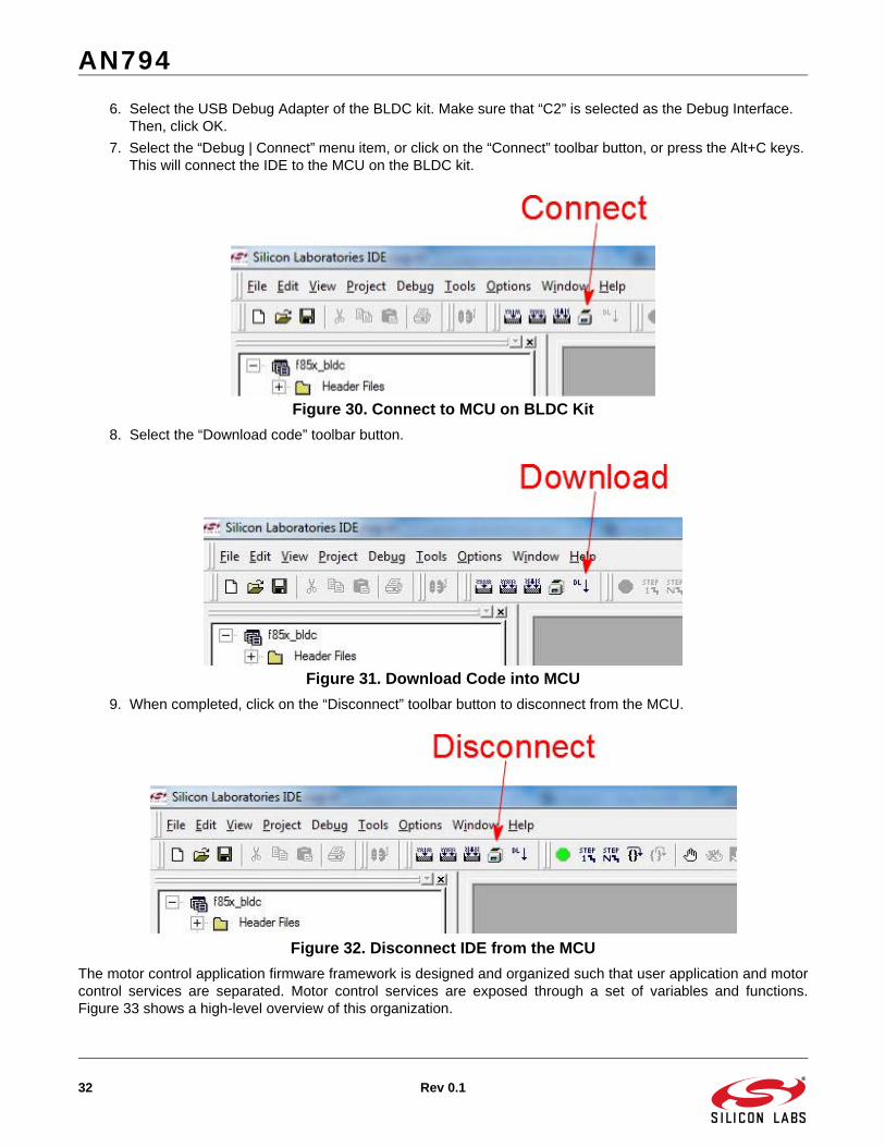
6. Select the USB Debug Adapter of the BLDC kit. Make sure that “C2” is selected as the Debug Interface. Then, click OK.
7. Select the “Debug | Connect” menu item, or click on the “Connect” toolbar button, or press the Alt+C keys. This will connect the IDE to the MCU on the BLDC kit.
Figure 30. Connect to MCU on BLDC Kit
8. Select the “Download code” toolbar button.
Figure 31. Download Code into MCU
9. When completed, click on the “Disconnect” toolbar button to disconnect from the MCU.
Figure 32. Disconnect IDE from the MCU
The motor control application firmware framework is designed and organized such that user application and motorcontrol services are separated. Motor control services are exposed through a set of variables and functions.Figure 33 shows a high-level overview of this organization.

AN794
Rev 0.1 33
Figure 33. Motor Control Application Firmware Framework
This framework simplifies the organization and implementation of user-specific application code. Users can writeapplication code to access the following services:
Standard C library
Standard C8051F85x peripheral registers such as CLKSEL, P0, P1.
Protothreads ServicesProtothreads are extremely lightweight, stackless threads developed by Adam Dunkels. More information can be
found at this website: http://dunkels.com/adam/ptThe Protothreads API are prefixed by PT_.
Motor control services. These are services provided to the application for the purpose driving the BLDC motor. There are 3 groups of API services:Functions. These are prefixed by SL_.Read-only variables. These are prefixed by SLR_.Read-write variables. These are prefixed by SLW_.
The firmware provided in the design kit is organized as follows:
Motor Application
Code
Motor Control Module
PCA control Module
Timer Management
Module
Application‐specific Peripheral Management
Module
Protothreads Services
User Code
Motor Control Services

AN794
34 Rev 0.1
Table 10. Categorization of BLDC Reference Design Firmware
Category Description Files
User Application This is the user application code. Users should re-implement the code here for their own applications. The default firmware is complex because it com-municates with the Silicon Labs Spinner over the UART interface and presents a register-based con-figuration interface.
btn.cmain.cMCP_core.cMCP_Registers.cmtrapp.cUART_Driver.cbldcdk.hbtn.hMCP_Core.hMCP_Registers.hmtrapp.hUART_Driver.h
Standard C8051F85x Services
Standard header files to access C8051F85x SFRs in a compiler-independent manner.
C8051F850_defs.hcompiler_defs.h
Protothreads Services An extremely lightweight, stackless, cooperative threading service.
lc.hlc-addrlabels.hlc-switch.hpt.hpt-sem.h
Motor Control Services These files implement the motor control services. Functions and variables that are accessible by user application are prefixed by SL_, SLR_, SLW_.BLDC_RD_Build_Params.h and BLDC_RD_Sys-tem.h can be modified to test out other operating modes – such has high-side PWM or low-side PWM modes. These 2 files are configuration files and they provide the configuration interface between the motor control module and the user application.The ADC module can be easily modified to read other user-defined voltages.
adc.cBLDC_RD_Build_Params.hBLDC_RD_System.hcomp.cmotor.cmtrpid.cadc.hpca.ctimers.ccomp.hmotor.hmtrpid.hpca.htimers.h

AN794
Rev 0.1 35
4.1. Motor Control APIThe motor control API functions consists of the following functions.
The motor control API also exports six read-only variables for the user application. These variables are prefixed bySLR_.
Table 11. Motor Control API Functions
Function Name Description
SL_MTR_init(void) Initializes the motor control variables and peripherals (PCA, timers, comparator). User application should call this function during MCU initialization. It initializes the motor state machine to the MOTOR_STOPPED state.
SL_MTR_motor(void) Executes the motor control state machine according to the motor state. User application should call this function regularly within its state machine or background loop.
SL_MTR_start_motor(void) This function starts the BLDC motor spinning if the motor is in the MOTOR_STOPPPED state.This function will first validate if the motor is still spinning. If the motor was still spinning in the desired direction, this function will start spin-ning the motor immediately. Otherwise, this function will align the motor in a known position before it starts spinning the motor. After starting the motor, the motor state machine is transitioned to the MOTOR_RUNNING state.
SL_MTR_stop_motor(void) This function stops energizing the coils of the BLDC motor if the motor is in the MOTOR_RUNNING state. The motor state machine will then be transitioned to the MOTOR_STOPPPED state.
SL_MTR_time(void) Gets the high 16-bit of the 32-bit running time of the system. Each time unit is 2.7 ms.
SL_MTR_GET_32BIT_TIME(x) A macro to read the 32-bit running time of the system and store in x. x is a UU32 type variable.
SL_MTR_change_pid_gain(pg, ig Initializes the PI proportional gain and PI integral gain parameters. The pro-portional gain is represented in units of 256/(SPEED_UNIT RPM). Refer to "4.5.9. Rotation Speed Resolution" on page 49 for definition of SPEED_UNIT. The integral gain has the same units based on a time resolu-tion unit of 1.
SL_MTR_change_num_poles(poles) Change the number of poles in the motor. This is normally not used in an actual application, but this is useful in a demo kit where users may wish to test a new motor without recompiling the firmware.

AN794
36 Rev 0.1
The motor control API exports writable variables for the user application to control the operation of the motorcontrol state machine. These variables are prefixed by SLW_.
Table 12. Motor Control API Read-Only Variables
Variable Name Description
SLR_motor_state Represents the state of the motor state machine. Can be one of 2 states: MOTOR_STOPPPED or MOTOR_RUNNING.
SLR_motor_current_rpm Represents the current motor rotation speed in units of (SPEED_UNIT x RPM). SPEED_UNIT is a user-configurable compile-time parameter to con-strain the maximum rotation speed to a 16-bit value.
SLR_pwm_duty Represents the duty cycle of the motor PWM signal. This value is a linear 16-bit quantity where 0xffff represents 100% duty cycle.
SLR_motor_stalled This is a 1-bit variable to indicate that the motor has stalled due to a system error event.
SLR_motor_current Average motor current measured by the sense resistor. This is expressed in units of 0.01 A.
SLR_motor_voltage Average motor supply voltage in units of 0.1 V. This is available only if FEA-TURE_MEAS_VMDC is enabled.
Table 13. Motor Control API Writable Variables
Variable Name Description
SLW_target_rpm This unsigned 16-bit variable is used only when the BLDC_RD_RP-M_OR_PWM macro is set to RPM_PARAMETER. This variable is used by the user application to indicate the target rotation speed that the motor control state machine should achieve. It is specified in units of (SPEED_UNIT * RPM).
SLW_target_pwm_duty This unsigned 16-bit variable is used only when the BLDC_RD_RP-M_OR_PWM macro is set to PWM_PARAMETER. This variable is used by the user application to indicate the target motor PWM duty cycle that the motor control state machine should achieve. This value is a linear quantity where 0xffff represents 100% duty cycle
SLW_acceleration_step_size This unsigned 16-bit variable is used only when the BLDC_RD_RP-M_OR_PWM macro is set to PWM_PARAMETER. This variable is used by the user application to indicate the rate at which the motor PWM duty cycle is incremented towards the target PWM duty cycle specified in the SLW_tar-get_pwm_duty variable.
SLW_deceleration_step_size This unsigned 16-bit variable is used only when the BLDC_RD_RP-M_OR_PWM macro is set to PWM_PARAMETER. This variable is used by the user application to indicate the rate at which the motor PWM duty cycle is decremented towards the target PWM duty cycle specified in the SLW_target_pwm_duty variable.
SLW_oc_debounce This is the overcurrent debounce count. This is normally not updated by the application. But this is useful in a demo kit where users may wish to test a new motor without re-compiling the firmware.

AN794
Rev 0.1 37
SLW_current_limit This is the maximum current limit in units of 0.01A. This is normally not updated by the application. But this is useful in a demo kit where users may wish to test a new motor without re-compiling the firmware.
SLW_motor_max_rpm This is the maximum RPM of the motor. This is normally not updated by the application. But this is useful in a demo kit where users may wish to test a new motor without re-compiling the firmware.
SLW_user_direction This is a 1-bit variable used by the user application to indicate to the motor control state machine the desired direction of rotation.
SLW_rpm_updated This is a 1-bit variable that the user application can test to check if the SLR_motor_current_rpm variable had been re-computed since the last time that this bit was cleared. The user application should clear this bit when it reads the SLR_motor_current_rpm variable.User application need not use this variable to read SLR_motor_cur-rent_rpm if the application does not care whether SLR_motor_cur-rent_rpm has been re-computed since the last time the variable was read.
SLW_pwm_updated This is a 1-bit variable that the user application can test to check if the SLR_pwm_duty variable had been modified since the last time that this bit was cleared. The user application should clear this bit when it reads the SLR_pwm_duty variable.User application need not use this variable to read SLR_pwm_duty if the application does not care whether SLR_pwm_duty has been re-computed since the last time the variable was read.
Table 13. Motor Control API Writable Variables (Continued)
Variable Name Description

AN794
38 Rev 0.1
4.2. Motor Control Demo Application Firmware FlowchartsThe flowcharts in this section provide a guide to the demo firmware application flow. The application developer canuse these flowcharts and "4.3. Typical Motor Control Implementation" on page 43 as guides to implement their ownapplication.
Figure 34. Demo Motor Application Top-Level Flowchart
AN794
Rev 0.1 39
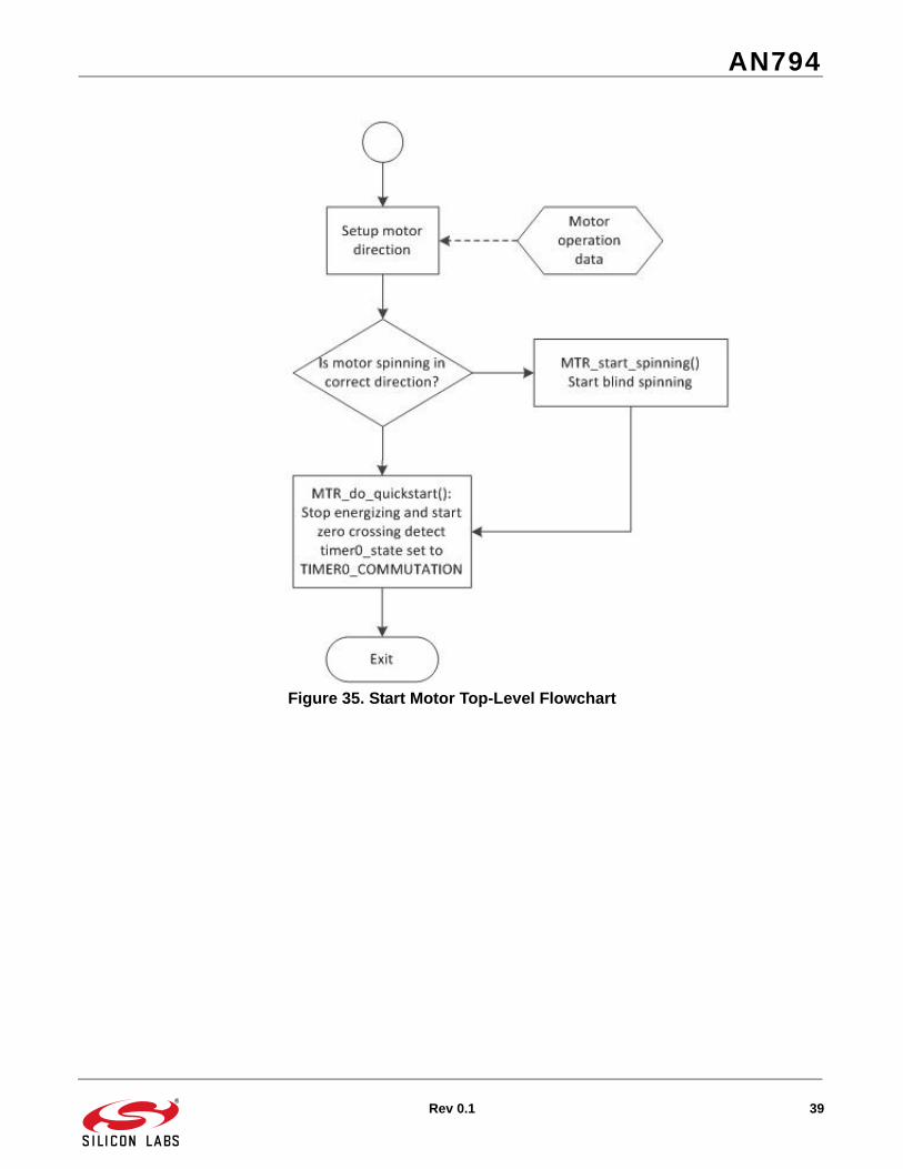
Figure 35. Start Motor Top-Level Flowchart

AN794
40 Rev 0.1
Figure 36. Run Motor Top-Level Flowchart

AN794
Rev 0.1 41
Figure 37. Timer 0 ISR Top-Level Flowchart
AN794
42 Rev 0.1
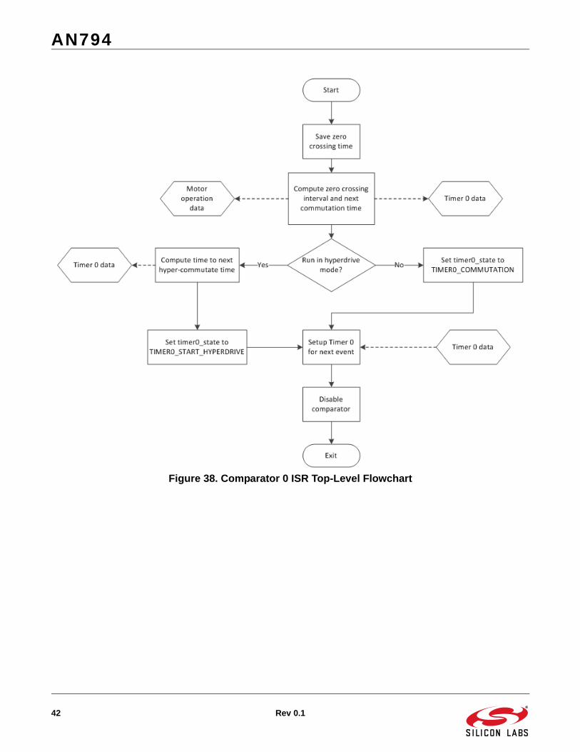
Figure 38. Comparator 0 ISR Top-Level Flowchart

AN794
Rev 0.1 43
4.3. Typical Motor Control ImplementationThe typical motor control application implementation is expected to be based on a standard non-blocking executionloop as shown in the following code sample:
void main() { // Application-specific peripheral initialization // …
// Initialize motor state machine and PID gain values SL_MTR_init(); SL_MTR_change_pid_gain(6000, 200);
while (1) { SL_MTR_motor();
if ( MOTOR_STOPPED == SLR_motor_state ) { /* Application-specific code for running state only such as: - determine target rotation direction - monitor motor voltage for undervoltage protection */ // …
if ( /* event to trigger start */ ) { // Initialize the Gains of PI controller SL_MTR_change_pid_gain(pgain, igain);
SL_MTR_start_motor(); // Start the motor
// Other application-specific code for start event – if any } } else if ( MOTOR_RUNNING == SLR_motor_state ) { /* Application-specific code for running state only such as:
- determine target rotation speed - monitor motor current for overcurrent detection - monitor motor voltage for undervoltage protection - check current motor speed */ // …
if ( /* event to trigger stop */ ) { SL_MTR_stop_motor(); // Stop the motor
// Other application-specific code for stop event – if any } }
// Application-specific code …
} }
AN794
44 Rev 0.1
4.4. Application Firmware ConfigurationThe default application provided in the kit can be configured for different modes of operation. These configurationsare defined in two header files, BLDC_RD_Build_Params.h and BLDC_RD_System.h. Users can modify thesefiles in any text editor and build the firmware for desired configuration. Some of the configurations defined inBLDC_RD_Build_Params.h can also be modified by the Silicon Labs Spinner.
Note that some of configurations may require changes to the jumper settings.
4.4.1. Speed Control Type
The firmware can be configured to accept 1 of 2 different types of speed control input: motor speed command orduty cycle of the motor PWM signal. The user can select the speed control type at build-time by defining:
#define BLDC_RD_RPM_OR_PWM XXX_PARAMETER
where XXX_PARAMETER can be one of the following:
RPM_PARAMETER—User selects motor rotation speed as the type of speed control user command.
PWM_PARAMETER—User selects motor PWM duty cycle as the type of speed control user command
This configuration is defined in BLDC_RD_Build_Params.h.
4.4.2. Speed Control Command Source
The firmware supports different input sources of the Speed Control Command:
External PWM signal
External analog signal (this is controlled by the potentiometer on the kit)
The user can select the speed control command source at build-time by defining:
#define BLDC_RD_RPM_PWM_SRC XXX_SPEED_SOURCE
where XXX_SPEED_SOURCE can be one of the following:
PWM_SPEED_SOURCE—External PWM signal sets the target value of Speed Control Parameter.
POT_SPEED_SOURCE—A potentiometer on BLDC kit sets the target value of Speed Control Parameter.
Note that configuring for PWM_SPEED_SOURCE or POT_SPEED_SOURCE requires a change in the jumpersetting at J108.
This configuration is defined in BLDC_RD_Build_Params.h.
4.4.3. Build for Protocol
The firmware implements a protocol to interact with the Silicon Labs Spinner. This protocol can be enabled at build-time by defining:
#define BUILD_FOR_PROTOCOL
This configuration is defined in BLDC_RD_Build_Params.h.
4.4.4. Overcurrent Detection
The kit firmware can measure current and detect over-current condition. This feature is enabled at build-time bydefining:
#define FEATURE_OVERCURRENT
If this feature is not required by user application then this line can be removed or commented. Note that this featureis automatically disabled if the FEATURE_PID_TUNE_FUNCTION is enabled - this is because of code memorylimitations.
When this feature is enabled, the current is measured on a user-assigned pin. This signal is assigned to P0.6 of theMCU in the BLDC kit. Users can configure the pin assignment as below:
#define IMEAS_ADCMX 6
When this feature is enabled, the appropriate PxMDIN assignment is automatically handled by thePxMDIN_INIT_VAL enumerated type definition in BLDC_RD_System.h header file.
AN794
Rev 0.1 45
When an op-amp is used to amplify current signal, the gain of the Op-Amp can also be configured as:
#define OP_AMP_GAIN (5.1/3.3)
If no op-amp is used, OP_AMP_GAIN should be set to 1.
These configurations are defined in BLDC_RD_System.h.
4.4.5. Motor Stall Detection
The motor stall detection is enabled at build-time by defining:
#define FEATURE_RPM_STALL_DETECTION
If this feature is not required by user application then this line can be removed or commented. This feature isautomatically disabled if BLDC_RD_RPM_OR_PWM is defined as PWM_PARAMETER. Motor stall condition isdetected by determining whether any increase in motor current is matched by a corresponding increase in motorspeed. Motor stall detection can be tuned by the following parameters:
#define STALL_CHECK_COUNT 100
#define COMPENSATION_CONSTANT_FACTOR (1UL * 65536UL / 100)
#define DELTA_CURRENT_FACTOR_K (70UL * 65536UL / (100UL * CURRENT_UNIT *MOTOR_MAX_CURRENT))
STALL_CHECK_COUNT defines the number of motor current samples to collect before the algorithm to detect stallis executed. To increase sensitivity to detect motor stall, users can either decrease:COMPENSATION_CONSTANT_FACTOR or increase: DELTA_CURRENT_FACTOR_K.
4.4.6. Motor Voltage Measurement
The kit firmware can measure the motor operating voltage. This feature is enabled at build-time by defining:
#define FEATURE_MEAS_VMDC
If this feature is not required by user application then this line can be removed or commented. Note that this featureis automatically disabled if the FEATURE_PID_TUNE_FUNCTION is enabled - this is because of code memorylimitations.
When this feature is enabled, the voltage is measured on a user-assigned pin. This signal is assigned to P0.7 ofthe MCU in the BLDC kit. Users can configure the pin assignment as below:
#define VMDC_ADCMX 7
When this feature is enabled, the appropriate PxMDIN assignment is automatically handled by thePxMDIN_INIT_VAL enumerated type definition in BLDC_RD_System.h header file.
These configurations are defined in BLDC_RD_System.h.
4.4.7. Potentiometer Measurement
The kit firmware can measure a voltage of a potentiometer - this is required if the speed control command source(section 4.3.2) is an analog voltage input. This feature is enabled at build-time by defining:
#define FEATURE_MEAS_POT
If this feature is not required by user application then this line can be removed or commented. When this feature isenabled, the voltage is measured on a user-assigned pin. This signal is assigned to P1.0 of the MCU in the BLDCkit. Users can configure the pin assignment as below:
#define POT_ADCMX 8
When this feature is enabled, the appropriate PxMDIN assignment is automatically handled by thePxMDIN_INIT_VAL enumerated type definition in BLDC_RD_System.h header file.
These configurations are defined in BLDC_RD_System.h.

AN794
46 Rev 0.1
4.4.8. Motor-Specific Configurations
In addition to BLDC_RD_NUM_POLES, following configurations depend on motor selected by user. Users shoulddefine additional headroom of 10% to 20% for the MOTOR_MAX_SPEED definition; this allows an opportunity forhyperdrive to kick in if this feature is enabled.
#define MOTOR_MAX_CURRENT 10.0
#define MOTOR_MAX_SPEED (54720)
#define MOTOR_MAX_RPM ((U16)(MOTOR_MAX_SPEED / SPEED_UNIT))
where MOTOR_MAX_CURRENT and MOTOR_MAX_SPEED are appropriate values given in the motor specificationsand system design.
These configurations are defined in BLDC_RD_System.h.
4.4.9. Buttons
The BLDC kit firmware supports a 2 button user interface: Button0 (SW101) and Button1 (SW102). The defaultapplication firmware uses Button0 for direction control (if Direction Command Source is configured to use button)and Button1 to start and stop the motor. These features can be enabled at build-time by defining:
#define FEATURE_BTN0
#define FEATURE_BTN1
If any button is not required by the user application then the corresponding line can be removed or commented.
When the button feature is enabled, the buttons are assigned to user-defined pins as:
#define BTN0_PORT P1
#define BTN0_BIT 1
#define BTN1_PORT P2
#define BTN1_BIT 1
The following helper macros will be defined to aid the user in writing firmware to use these buttons:
CONFIG_BTN0()
IS_BTN0_PRESSED()
CONFIG_BTN1()
IS_BTN1_PRESSED()
But if the button feature is not enabled, then the corresponding CONFIG_BTNx() macro will be empty andIS_BTNx_PRESSED() will always return 0.
These configurations are defined in BLDC_RD_System.h.

AN794
Rev 0.1 47
4.5. Motor Control Module ConfigurationWhen users are ready to implement their motor control design and application, the default application and designas supplied by the kit is not likely to be compatible to their requirements - for example, BLDC fans do not normallyhave buttons. The kit provides design-specific configuration of the motor control module (motor.c, mtrpid.c) fordifferent modes of operation. These configurations are defined in two header files, BLDC_RD_Build_Params.h andBLDC_RD_System.h. Users can modify these files in any text editor and build the firmware in a suitableconfiguration.
4.5.1. PWM Scheme
The firmware supports 3 different PWM schemes: high-side, low-side or mixed mode. The different PWM schemesare discussed earlier in section 2.2. The user can select the PWM scheme at build-time by defining:
#define BLDC_RD_PWM_METHOD H_BRIDGE_XXX_PWM
where H_BRIDGE_XXX_PWM can be one of the following:
H_BRIDGE_HIGH_SIDE_PWM - High-side only PWM.
H_BRIDGE_LOW_SIDE_PWM - Low-side only PWM.
H_BRIDGE_MIXED_MODE_PWM - Mixed-mode PWM.
This configuration is defined in BLDC_RD_Build_Params.h.
4.5.2. Commutation Method
The firmware supports 2 different methods of commutation: zero-crossing timing, or detection by Hall sensors. Theuser can select the commutation method at build-time by defining:
#define BLDC_RD_COMMUT_METHOD COMMUTATION_BY_XXX
where COMMUTATION_BY_XXX can be one of the following:
COMMUTATION_BY_COUNTDOWN - Commutate using zero-crossing timing method.
COMMUTATION_BY_HALL - Commutate using detection by Hall sensors method.
This configuration is defined in BLDC_RD_Build_Params.h.
4.5.3. Number of Poles
Different BLDC motors are constructed with different number of poles. The motor rotation speed is calculatedbased on the number of poles. The user can select the number of poles at build-time by defining:
#define BLDC_RD_NUM_POLES N
where N is the number of poles. If motor specification mentions pole-pairs then N should be two times that number.
This configuration is defined in BLDC_RD_Build_Params.h.
4.5.4. Frequency Generator Signal
This configuration enables FG feature - a feature commonly used in fan applications to output a digital signal thattoggles ever 3 commutations (i.e. 1 cycle every 1 motor electrical cycle). This feature is enabled at build-time as:
#define FEATURE_FG
If the FG signal is not required by user application then this line can be removed or commented.
When this feature is enabled, it generates FG signal on a user-assigned pin. This signal is assigned to P2.0 of theMCU in the BLDC kit. Users can configure the pin assignment as below:
#define FG_PORT P2
#define FG_BIT 0
When this feature is enabled, the following macros will be defined:
CONFIG_FG()
SET_FG()
CLR_FG()
TOGGLE_FG()

AN794
48 Rev 0.1
These macros will be used by the motor control module to toggle the FG pin - so users need not change the motorcontrol source code to use this feature. If this feature is not required (i.e. FEATURE_FG is not defined), then thesemacros will be empty - hence, no code is generated even though the motor control source code call these macros.
All these configurations are defined in BLDC_RD_System.h.
4.5.5. Motor Startup Current Control Pin
The kit firmware implements a motor startup technique that is based on limiting the current through the motor (seesection 3.5). This requires some form of motor current measurement to be available to the MCU so that thecomparator CMP0 can be used to implement this feature. This motor current measurement pin must be assignedto a pin on Port 0 because only CMP0 implements the comparator clear functionality. It is possible to assign this pinto the same pin as the over current detection pin (see "4.4.4. Overcurrent Detection" on page 44). This pin isassigned to P0.6 of the MCU in the BLDC kit. Users can configure the pin assignment as below:
#define CPT0MX_IMEASURE 6
This configuration is defined in BLDC_RD_System.h.
4.5.6. Hyperdrive Mode
The hyperdrive mode can be used to achieve higher speed. This feature is enabled at build-time by defining:
#define FEATURE_HYPERDRIVE
If this feature is not required by user application then this line can be removed or commented. Note that this featureis automatically disabled if the FEATURE_PID_TUNE_FUNCTION is enabled - this is because of code memorylimitations.
These configurations are defined in BLDC_RD_System.h.
4.5.7. Motor Gate Drive Peripheral Assignment
One PCA channel is used to generate the motor PWM signal. This PCA channel can be modified by users for theirapplication:
#define MOTPWM_CHANNEL 1
Note that channel 0 is reserved for blanking signal.
The motor gate drive pins must be assigned to Port 1, but the pins can be assigned by users for their design asfollows:
#define MOTDRV_AL_PIN 2
#define MOTDRV_AH_PIN 3
#define MOTDRV_BL_PIN 4
#define MOTDRV_BH_PIN 5
#define MOTDRV_CL_PIN 6
#define MOTDRV_CH_PIN 7
The active level of the motor gate drive pins can also be defined as high (1) or low (0) to match the hardwaredesign:
#define MOTDRV_LOW_ACT 1
#define MOTDRV_HIGH_ACT 1
These configurations are defined in BLDC_RD_System.h.
4.5.8. Filtered Back-EMF Pins
The filtered back-EMF signals can be assigned to Port 0 pins by users for their design:
#define FILTERED_A_PIN 0
#define FILTERED_B_PIN 1
#define FILTERED_C_PIN 2
#define FILTERED_Y_PIN 3
These configurations are defined in BLDC_RD_System.h.

AN794
Rev 0.1 49
4.5.9. Rotation Speed Resolution
The BLDC kit supports motor rotation speeds of up to 200000 RPM. However, the firmware uses only 16-bitvariables for motor speed to optimize code memory and speed. Hence, to support high speeds, the firmwaredefines the smallest unit of RPM that the system measures as:
#define SPEED_UNIT 10
This configuration is defined in BLDC_RD_System.h. The Spinner application assumes this value to be 10.
AN794
50 Rev 0.1
5. Silicon Labs Spinner
The Silicon Labs Spinner provides a GUI interface to configure some of the build-time parameters in the firmware.The changes must be recompiled into a new firmware and downloaded into the MCU. The tool also provides aninterface to view run-time parameters and plot them in real-time.
5.1. Build-Time ConfigurationBuild-time configurations are set in the Create New Project dialog. This dialog is activated through the “File |Create New Project...” menu item. When Generate Project button is clicked (after selecting appropriateconfigurations), the entire firmware project is created in the project directory with new settings withinBLDC_RD_Build_Params.h. Users can use the Silicon Labs IDE to open the workspace f85x_bldc.wsp in theproject directory to rebuild a new firmware image.
Figure 39. Silicon Labs Spinner Build-Time Configuration
Most of the build-time configuration has been covered in "4.3. Typical Motor Control Implementation" on page 43.The”Project Directory” text box field lets the user specify the directory in which the firmware project should begenerated.

AN794
Rev 0.1 51
5.2. Runtime Monitor and ControlRun-time parameters can be read, plotted, and set to desired values using the Easy Mode view or the AdvancedMode view. The appropriate view can be selected from the View menu.
Figure 40. Easy Mode View
After the BLDC kit is powered and connected to a host PC, the user can establish a session with the BLDC kit tooperate the motor. This is accomplished by performing the following steps with the application (Easy Mode view):
1. Connect a USB cable between the PC and the MCU board.
2. Apply power to the powertrain board (must be done after Step 1).
3. Use Device Manager to identify the COM Port: “Silicon Labs CP210x USB to UART Bridge”.
4. Select the COM port found in Step 3, and click the “Connect” button.
5. Select the appropriate rotational direction.
6. Select the target motor speed.
7. Click the “Start Motor” button to run the motor.
8. The user can change the target motor speed while the motor is running.
9. The user can click the “Stop Motor” button to stop the motor while the motor is running.
10. The user can also press the “Start/Stop” pushbutton on the board to stop the motor while the motor is running. Refer to Figure 44, “User Interface for Standalone Operation of BLDC Demo Kit,” on page 55 for the location of this pushbutton on the board.
The “Configuration Settings” button allows the user to change the “Maximum Motor Speed” and “Pole Pairs”parameters; these parameters must be changed when testing a different motor model.
AN794
52 Rev 0.1
Figure 41. Advanced Mode View
In the Advanced Mode view, there are more parameters available for the user to change. The “Get” buttons allowthe user to read parameters from the MCU, and the “Set” buttons allow the user to write parameters to the MCU.These parameters have been discussed in "4.4. Application Firmware Configuration" on page 44 and "4.5. MotorControl Module Configuration" on page 47.
AN794
Rev 0.1 53
6. Operating Another BLDC Motor
The kit can be used to operate any 3-phase BLDC motor that conforms to the following operation limits:
Maximum Motor voltage: < 24 Vdc
Maximum average current: < 10 A
Maximum speed: 200000 RPM or lower for a 2-pole BLDC motor
If the motor current is expected to exceed 5 A, then a suitable external power supply must be used as a powersource for the kit. The power source can be connected through one of the two power connections shown inFigure 42.
Figure 42. Power Source Options for BLDC Demo Kit
The power supply and the USB connection to PC must be connected in the following sequence:
1. Connect USB to PC; then
2. Apply power to the powertrain board
The user must run the Silicon Labs Spinner to connect to the kit and change 2 key parameters to match the motorspecifications:
Number of poles in the motor
Maximum operation speed of the motor (i.e. Maximum RPM)

AN794
54 Rev 0.1
Click on the “Configuration Settings” button in the Easy Mode view to change these two parameters.
Figure 43. Pending Screenshot
After these two parameters have been changed to match the motor specifications, the user can operate the motorusing the Start/Stop button, Direction button and potentiometer as shown in Figure 44.

AN794
Rev 0.1 55
Figure 44. User Interface for Standalone Operation of BLDC Demo Kit
The details of the user interface behavior are described in Table 14.
Table 14. BLDC Motor Kit user Interface for Standalone Operation
User Interface Description
SW101 Pushbutton. Controls the direction of rotation of the motor. Pressing this button reverses the direction of rotation. This button is read by the firmware only when the motor is not running.
SW102 Pushbutton. Starts/stops the motor.
SW301 Pushbutton. Reset button of the C8051F850
R109 Rotary potentiometer. Controls the speed of the motor. Clockwise direction increases the speed of the motor.
TP308 Header pin. This is the C2D pin of the F850. The motor firmware synchronizes output of this pin with the electrical cycle of the motor so that the user can monitor the speed of rotation of the motor. The rotor speed can be calculated by this formula:
Rotor speed (RPM) = (Frequency of TP308 in Hz) x 120 / (Number of poles in motor)

AN794
56 Rev 0.1
7. Hardware Design Guide
There are a few key design parameters to observe in the hardware design if the user wishes to take advantage ofthe unique features of the C8051F850 and the firmware. The kit includes a spreadsheet tool to guide the user toselect the optimal resistor values to use in the design. The spreadsheet is located in <Install Directory>\F850-BLDC-RD\DesignTools\bldcdesign.xlsx, where <Install Directory> is C:\Silabs\MCU if the default option is chosenduring installation.
7.1. Design of Op-amp Gain for Current Sense Circuit"3.2.3. Current Sensing Circuit" on page 24 discussed the operation of the current sense circuit, while "3.5. BLDCMotor Startup Technique" on page 28 explained how the current sensing is applied in the motor startup techniqueas used by the firmware. The design of the op-amp gain and offset is such that 2 times the maximum motor currentwill result in a 1.8 V output at the op-amp. The design goal is to match the op-amp voltage output to the internalC8051F850 comparator voltage reference (1.8 V) so that this voltage can be used as the trip point for the motorstartup technique without using an additional pin to provide a voltage reference. The spreadsheet tool included inthe kit can be used to guide the user to select the correct resistor values for the op-amp circuit.
7.2. Design of BEMF Zero-Crossing Detection CircuitSections "3.1.2. Back-EMF Filter Circuit" on page 21 and "3.1.3. Virtual Neutral Filter Circuit" on page 22 describethe Back-EMF filter circuit and the Virtual neutral filter circuit respectively. The design goals of these two circuits areas follows:
The filtered voltages do not exceed the MCU operating voltage even when the motor supply voltage is at maximum voltage. The design tool allows the designer to specify some headroom to compensate for voltage spikes at the motor terminals.
The offset of the 2 circuits must be the same (see equations 37 and 38 for the offset voltage formula)
The gain of the virtual neutral filter circuit must be 1/3 of the gain of the BEMF filter circuit
The spreadsheet tool includes an option to reduce the number of resistors in the virtual neutral resistor networkfrom 9 resistors to 5 resistors. This option is meant for designs that have limited PCB space for layout of allcomponents. This trades off a slight inaccuracy in the zero-crossing detection in return for reduced componentcount and PCB footprint.
7.3. Low-Cost, Low-Current DesignThe powertrain of the reference design kit was based on a design that had to operate at 80 V motor voltage. Thedesign of this kit was then scaled down to meet the requirements of the design kit (24 V, 10 A). However, it ispossible to reduce costs further in some applications.
Figure 53 on page 65 shows a schematic of a low-cost version of a design for low-current motors. The key changesin this version are:
Replace high-side N-channel power MOSFETs with P-channel MOSFETs. This simplifies the design and lowers the cost of the high-side gate drivers.
Replace the Si8230 isolated gate drivers with discrete components.
The spreadsheet tool includes a guide to help users design the gate drivers of these MOSFETs.

AN794
Rev 0.1 57
8. Schematics
8.1. Powertrain Board Schematics
Arra
ngem
ent in
dicat
es p
hysic
al pla
cem
ent
Wall
Ada
pter
Jack
+12V
to ra
ted
volta
geup
to 5
A
Term
inal B
lock
+12
to ra
ted
volta
geup
to 1
0 AW
G W
ire
Mot
or T
erm
inal B
lock
up to
10
AWG
Wire
Plac
e te
stpoin
tsne
ar te
rmina
lsPl
ace
testp
oints
near
term
inals
All c
aps 5
0V u
nless
not
ed
Q4-
SQ
5-S
Q6-
S
MTR
_VD
C
PW
R_G
ND
MTR
_VD
C
PW
R_G
ND
MC
U_G
ND
MTR
_VD
C
PW
R_G
ND
PW
R_G
ND
MTR
_VD
C
IM_0
P
IM_0
N
MTR
_VA
PH
A_V
OA
IM_1
P
IM_1
N
MTR
_VB
IM_2
P
IM_2
N
MTR
_VC
PH
A_G
ND
A
PH
A_G
ND
B
PH
A_V
OB
PH
B_G
ND
A
PH
B_G
ND
B
PH
B_V
OB
PH
B_V
OA
PH
C_G
ND
A
PH
C_G
ND
B
PH
C_V
OB
PH
C_V
OA
MTR
_VA
MTR
_VB
MTR
_VC
MTR
_VA
MTR
_VB
MTR
_VC
J1
S19
11-4
6R
C5
4.7u
F10
0V
R1
50m
Ohm
R14
0
R4
8.2
C6
4.7u
F
100V
Q6
IRFH
7446
TR2P
BF
40V
4
12
3
56
78
9
R17
NI
R2
NI
R21
NI
TP5
G5
3x6.
35m
m
J61 2 3
J4 Pow
er J
ack
1 23
TP4
G4
R7
8.2
C9
1uF
100V
R10
0
C8
1uF
100V
R20
NI
+C
215
00uF
35V
+C
115
00uF
35V
TP9
MTR
_VB
TP3
G3
R12
0
2x6.
35m
m
J51 2
R6
8.2
R13
0
R15
0
C7
1uF
100V
TP6
G6
TP11
MTR
_VC
TP10
PW
R_G
ND
J3
NI
R9
8.2
R5
8.2
Q1
IRFH
7446
TR2P
BF
40V
4
12
3
56
78
9
R16
0
C3
4.7u
F10
0V
TP2
G2Q2
IRFH
7446
TR2P
BF
40V
4
12
3
56
78
9
TP8
MTR
_VD
C
R8
8.2
Q3
IRFH
7446
TR2P
BF
40V
4
12
3
56
78
9
R19
0
C4
4.7u
F10
0V
R11
0
TP7
MTR
_VA
R22
0
Q4
IRFH
7446
TR2P
BF
40V
4
12
3
56
78
9
R18
NI
R3
NI
J2
S19
11-4
6R
TP1
G1
Q5
IRFH
7446
TR2P
BF
40V
4
12
3
56
78
9
Fig
ure
45.P
ow
ertr
ain
Bo
ard
Sch
emat
ic (
1 o
f 3)

AN794
58 Rev 0.1
]
Rate
d Vo
ltage
on
mot
or =
1.0
V to
MCU
Rate
d vo
ltage
on
all th
ree
phas
es =
1.0
V to
MCU
All c
aps 5
0V u
nless
not
ed
MC
U_G
ND
+12V
+5V
MC
U_G
ND
MC
U_G
ND
MC
U_G
ND+3
.3V
MC
U_G
ND
MC
U_G
ND
MC
U_G
ND
MC
U_G
ND
MC
U_G
ND
MC
U_G
ND
MC
U_G
ND
+12V
MC
U_G
ND
+5V
MC
U_G
ND
MC
U_G
ND
MC
U_G
ND
+3.3
V
MC
U_G
ND
+12V
MC
U_G
ND
+5V
MC
U_G
ND
MC
U_G
ND
MC
U_G
ND
+3.3
V
MTR
_VD
C+3
.3V
+3.3
V
PH
A_G
ND
A
PH
A_G
ND
B
PH
A_V
OB
PH
A_V
OA
PW
M0A
PW
M0B
GD
0_E
N/
VM
A
MTR
_VA
VM
B
MTR
_VB
VM
C
MTR
_VC
VM
DC
MTR
_VA
MTR
_VB
MTR
_VC
VM
Y
PW
M1A
PW
M1B
GD
1_E
N/
PH
B_G
ND
A
PH
B_G
ND
B
PH
B_V
OB
PH
B_V
OA
PW
M2A
PW
M2B
GD
2_E
N/
PH
C_G
ND
A
PH
C_G
ND
B
PH
C_V
OB
PH
C_V
OA
VM
AV
MB
VM
CV
MD
C
VM
Y
R54
0
D3
MB
R1H
100S
F
R55 N
I
C20
1uF
C11
100p
F
R70
5.1K
U2
Si8
230
VIA
/PW
M1
VIB
2
GN
DI
4
NC
7
DIS
AB
LE5
VO
B10
VD
DI
8G
ND
B9
NC
12
VD
DB
11
VD
DI
3
DT
6
NC
13G
ND
A14
VO
A15
VD
DA
16
R27
1.15
K
R74
5.1K
R26
9.76
K
R43
10K
R36
1.15
K
C16
1uF
R40
1.0
R48
4.7K
R32
9.76
K
C10
100p
F
U3
Si8
230
VIA
/PW
M1
VIB
2
GN
DI
4
NC
7
DIS
AB
LE5
VO
B10
VD
DI
8G
ND
B9
NC
12
VD
DB
11
VD
DI
3
DT
6
NC
13G
ND
A14
VO
A15
VD
DA
16
R28
1.15
K
R44
10K
R51
4.7K
R71
5.1K
C14
100p
F
C17
1uF
R42
1.0
C12
100p
F
R37
1.0
C22
1uF
R56 N
I
R29
1.15
K
R31
9.76
K
R33
9.76
K
R45
10K
R46
4.7K
R34
1.15
K
R68
5.1K
R30
1.15
K
R39
1.0
R72
5.1K
U1
Si8
230
VIA
/PW
M1
VIB
2
GN
DI
4
NC
7
DIS
AB
LE5
VO
B10
VD
DI
8G
ND
B9
NC
12
VD
DB
11
VD
DI
3
DT
6
NC
13G
ND
A14
VO
A15
VD
DA
16
C23
1uF
R57 N
I
C19
1uF
R50
4.7K
C13
100p
F
R23
9.76
K
C18
1uF
R47
4.7K
R52
0
R38
1.0
R41
1.0
R53
0
D2
MB
R1H
100S
F
R24
9.76
KR
695.
1K
C21
1uF
C15
1uF
R73
5.1K
R35
1.15
K
R49
4.7K
R25
9.76
K
D1
MB
R1H
100S
F
Fig
ure
46.P
ow
ertr
ain
Bo
ard
Sch
emat
ic (
2 o
f 3)
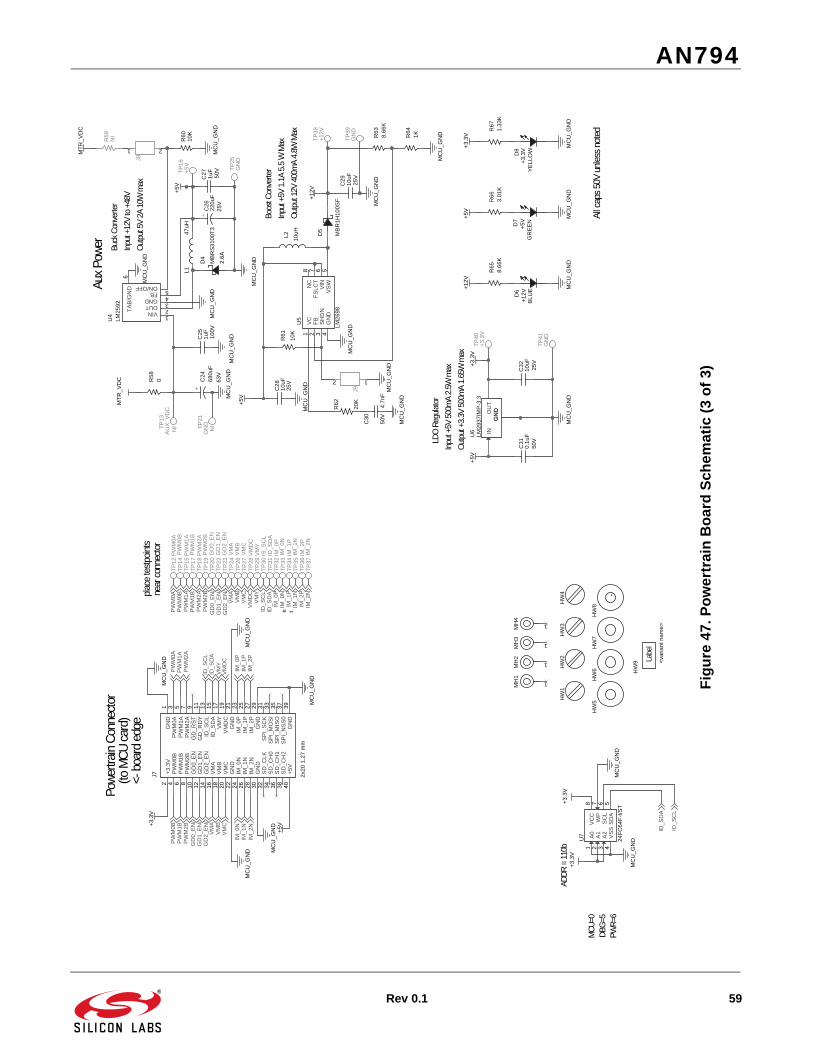
AN794
Rev 0.1 59
Powe
rtrain
Con
necto
r
<- b
oard
edg
e
Aux P
ower
ADDR
= 1
10b
(to M
CU ca
rd)
Inpu
t +12
V to
+48
VBu
ck C
onve
rter
Outp
ut 5
V 2A
10W
max
Outp
ut 1
2V 4
00m
A 4.
8W M
axIn
put +
5V 1
.1A
5.5
W M
axBo
ost C
onve
rter
Outp
ut +
3.3V
500
mA
1.65
W m
axIn
put +
5V 5
00m
A 2.
5W m
axLD
O Re
gulat
or
place
testp
oints
near
conn
ecto
r
All c
aps 5
0V u
nless
not
ed.
DBG=
5M
CU=0
PWR=
6
+5V
MC
U_G
ND
+3.3
V
MC
U_G
ND
MC
U_G
ND
MC
U_G
ND
+3.3
V
MC
U_G
ND
+5V
MC
U_G
ND
+3.3
V+3
.3V
MC
U_G
ND
MC
U_G
ND
MC
U_G
ND
MC
U_G
ND
MC
U_G
ND
MC
U_G
ND
+5V
+5V
MC
U_G
ND
MC
U_G
ND
MC
U_G
ND
+5V
+12V
MC
U_G
ND
MC
U_G
ND
MC
U_G
ND
+12V
+3.3
V
MC
U_G
ND
MC
U_G
ND
MC
U_G
ND
MC
U_G
ND
MTR
_VD
C
MTR
_VD
C
MC
U_G
ND
IM_0
PIM
_0N
IM_1
PIM
_1N
IM_2
NIM
_2P
VM
BV
MA
VM
CV
MY
VM
DC
PW
M0A
PW
M1A
PW
M0B
PW
M2A
PW
M1B
PW
M2B
ID_S
CL
ID_S
CL
ID_S
DA
ID_S
DA
GD
0_E
N/
GD
1_E
N/
GD
2_E
N/
GD
0_E
N/
GD
1_E
N/
GD
2_E
N/
IM_0
PIM
_0N
IM_1
PIM
_1N
IM_2
NIM
_2P
VM
BV
MA
VM
C
VM
YV
MD
C
PW
M0A
PW
M1A
PW
M0B
PW
M2A
PW
M1B
PW
M2B
ID_S
CL
ID_S
DA
e t
TP26
VM
B
D7
GR
EE
N+5
V
C30
4.7n
F50
V
TP19
PW
M2B
MH
4
1
HW
6
TP28
VM
DC
TP16
+5V
TP40
+3.3
V
R65
8.66
K
TP30
IS_S
CL
HW
5
LM26
98
U5
VC
1
FB2
SH
DN
3
GN
D4
NC
8
FSLC
T7
VIN
6
VS
W5
R64
1K
TP12
PW
M0A
R61
10K
+C
2622
0uF
25V
U6
LM29
37IM
P-3
.3
GN
DIN
OU
TG
ND
TP25
GN
D
D4
MB
RS
3100
T3
TP38
+12V
C32
10uF
25V
TP33
IM_0
N
MH
1
1
TP22
GD
1_E
N
Labe
l
HW
9 <var
iant
nam
e>
C28
10uF
25V
+C
2468
0uF
63V
R66
3.01
K
TP13
AU
X_V
DC
NI
TP17
PW
M1B
TP41
GN
D
R60
10K
C29
10uF
25V
C31
0.1u
F50
V
TP18
PW
M2A
C25
1uF
100V
D8
YE
LLO
W+3
.3V
TP34
IM_1
P
HW
4
MH
3
1
2x20
1.2
7 m
m
J7 +3.3
V2
PW
M0B
4
PW
M1B
6
PW
M2B
8
GD
0_E
N10
GD
1_E
N12
GD
2_E
N14
VM
A16
VM
B18
VM
C20
GN
D22
IM_0
N24
IM_1
N26
IM_2
N28
GN
D30
SD
_CLK
32
SD
_CH
034
SD
_CH
136
SD
_CH
238
+5V
40
GN
D1
PW
M0A
3
PW
M1A
5
PW
M2A
7
GD
_RS
T9
GD
_RD
Y11
ID_S
CL
13
ID_S
DA
15
VM
Y17
VM
DC
19
GN
D21
IM_0
P23
IM_1
P25
IM_2
P27
GN
D29
SP
I_S
CK
31
SP
I_M
OS
I33
SP
I_M
ISO
35
SP
I_N
SS
037
GN
D39
D5
MB
R1H
100S
F
TP24
VM
A
HW
3
TP29
VM
Y
TP37
IM_2
N
TP39
GN
D
TP20
GD
0_E
N
R62
20K
HW
2
U7
24FC
64F-
I/ST
A0
1
A1
2
A2
3
VS
S4
VC
C8
SD
A5
SC
L6
WP
7
TP31
ID_S
DA
TP21
GN
DN
IC
27 1uF
50V
L2 10uH
HW
1
R63
8.66
K
LM25
92U
4
VIN1
OUT2
GND3
FB4
ON/OFF5
TAB
/GN
D6
TP32
IM_0
P
J9
12
R67
1.33
K
TP27
VM
C
R59
NI
TP35
IM_1
N
TP23
GD
2_E
N
TP14
PW
M0B
J8
1 2
TP15
PW
M1A
D6
BLU
E+1
2VM
H2
1
R58
0
L147
uH
2.6A
HW
8H
W7
TP36
IM_2
P
Fig
ure
47.P
ow
ertr
ain
Bo
ard
Sch
emat
ic (
3 o
f 3)

AN794
60 Rev 0.1
8.2. MCU Board Schematics
Fig
ure
48.M
CU
Bo
ard
Sch
emat
ic

AN794
Rev 0.1 61
Gai
n =
1.5
5
Vbia
s =
0.2
75V
+ -
3 21
U20
1-A
LMV8
42M
M/N
OPB
+ -
5 67
48
U20
1-B LM
V842
MM
/NO
PB
R208
3.3K
R209
3.3K
R205
5.1K
R207
5.1K
R202
10K
R203
910
C202
NI
C203 NI
C204
0.1u
F
J202DO NOT INSTALL
R201
NI
J201DO NOT INSTALL
R204
NI
R206 NI
J203
DO
NO
T IN
STAL
L
C201
0.1u
F
GND
+3.
3V
+3.
3V
GND
IM_0
N
IM_0
P
I_M
EAS
GND
GND Fig
ure
49.O
pA
mp
Sch
emat
ic
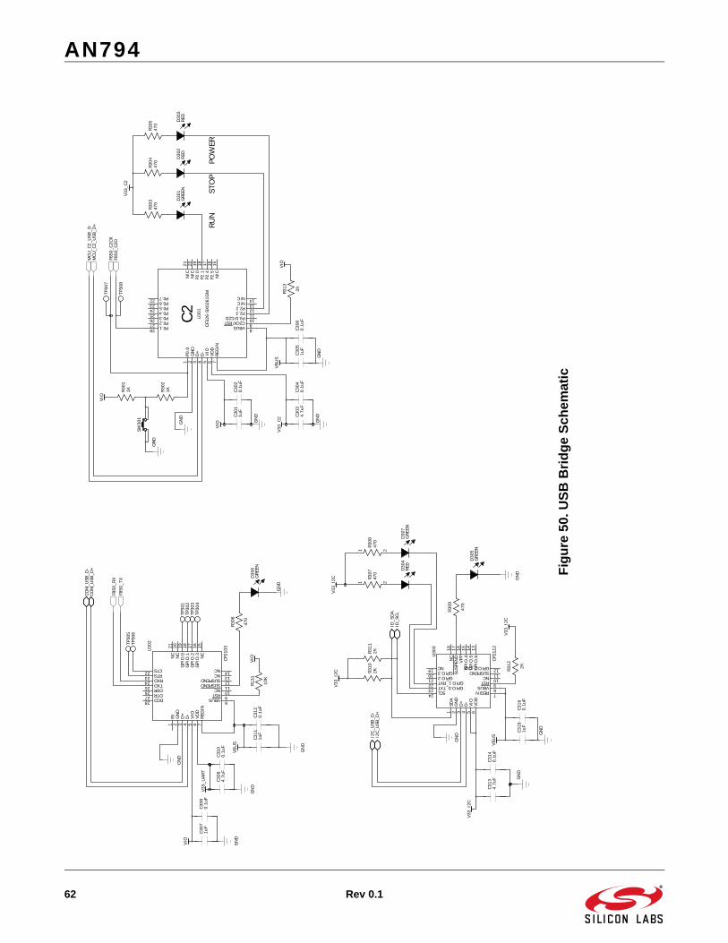
AN794
62 Rev 0.1
RUN
STO
PPO
WER
C21
P0.0
2GND
3D+
4D-
5VI
O6
VDD
7RE
GIN
8VBUS 9C2CK/RST 10P3.0/C2D 11P2.3 12P2.2 13N/C 14N/C
15N/C
16P2
.517
P2.4
18P2
.119
P2.0
20N/C
21N/C
22 P0.723 P0.624 P0.525 P0.426 P0.327 P0.228 P0.1
U30
1
CF32
6-SX
0261
GM
C301
1uF
C302
0.1u
F
C303
4.7u
FC3
040.
1uF
R303
470
R304
470
R305
470
R313 2K
C306
0.1u
F
1SD
A2
GND
3D+
4D-
5VI
O6
VDD
7REGIN 8VBUS 9RST 10NC 11SUSPEND 12GPIO.7_CLK
13GPI
O.6
14GPI
O.5
15GPI
O.4
16VP
P17
SUSP
END
18NC
19 NC20 GPIO.321 GPIO.222 GPIO.1_RXT23 GPIO.0_TXT24 SCL
U30
3
CP21
12
1RI
2GND
3D+
4D-
5VI
O6
VDD
7RE
GIN
21NC
20NC
19GPI
O.0
18GPI
O.1
17GPI
O.2
16GPI
O.3
15NC
22 CTS23 RTS24 RXD25 TXD26 DSR27 DTR28 DCD
14NC13NC12SUSPEND11SUSPEND10NC9RST8VBUS
U30
2
CP21
03C3
094.
7uF
C310
0.1u
F
R131
10K
C312
0.1u
F
R306
470
C313
4.7u
FC3
140.
1uF
R301
1K R302
1K
C305
1uF
C311
1uF C3
151u
F
R309
470
C307
1uF
C308
0.1u
F
R312 2K
R310
2KR3
112K
1 2
R307
470
1 2
R308
470
C316
0.1u
F
D30
1GRE
END30
2RE
DD30
3RE
D
D30
4RE
D
D30
5GRE
EN
D30
6GRE
EN
D30
7GRE
EN
SW30
1
TP30
1TP
302
TP30
3TP
304
TP30
5TP
306
TP30
7
TP30
8
GND
VIO G
ND
V33_
C2
V33_
C2
VIO
GND
V33_
UAR
T
VIO
COM
_USB
_D+
COM
_USB
_D-
GND
GND
MCU
_C2_
USB
_D-
MCU
_C2_
USB
_D+
F850
_RX
F850
_TX
GND
F850
_C2C
KF8
50_C
2D
GND
VIO
VBUS G
ND
VBUS
GND VB
US G
ND
V33_
I2C
GND
GND
VIO
I2C_
USB
_D-
I2C_
USB
_D+
GND
V33_
I2C
ID_S
CLID
_SDA
V33_
I2C
V33_
I2C
GND
Fig
ure
50.U
SB
Bri
dg
e S
chem
atic

AN794
Rev 0.1 63
Fig
ure
51.U
SB
Hu
b S
chem
atic
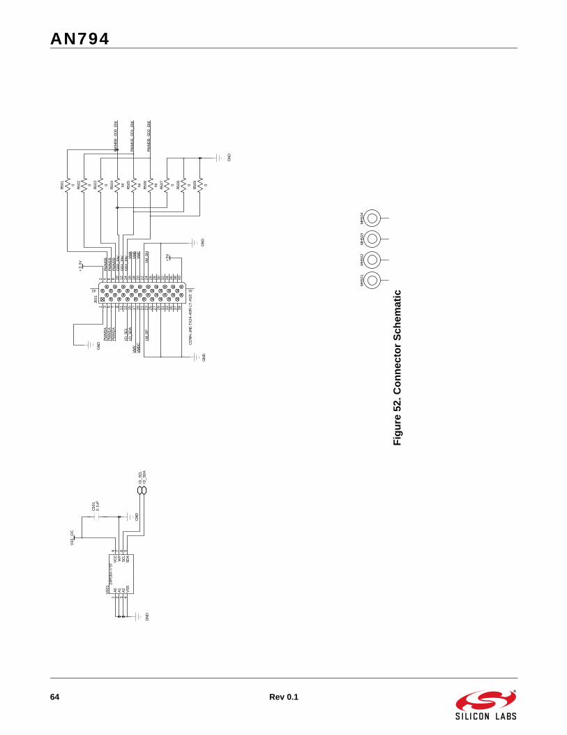
AN794
64 Rev 0.1
1A0
2A1
3A2
4VS
S5
SDA
6SC
L7
WP
8VC
C
U50
1 24FC
64-I
/ST
C501
0.1u
F
R501 0
R502 0
R503 0
R504 NI
R505 NI
R506 NI
R507 0
R508 0
R509 0
MH50
1M
H50
2M
H50
3M
H50
4
12
34
56
78
910
1112
1314
1516
1718
1920
2122
2324
2526
2728
2930
3132
3334
3536
3738
3940
4142
J501
CONN-J
AE-T
X24-
40R-
LT-H
1E
GND
+3.
3V
PWM
0APW
M1A
PWM
2A
VMA
VMB
VMC
ID_S
CLID
_SDA
VMY
VMDC
GND
GND
+5V
V33_
I2C
GND
ID_S
CLID
_SDA
GND
PWM
2B_G
D2_
EN/
PWM
1B_G
D1_
EN/
PWM
0B_G
D0_
EN/
GND
PWM
0BPW
M1B
PWM
2BGD0_
EN/
GD1_
EN/
GD2_
EN/
IM_0
PIM
_0N
Fig
ure
52.C
on
nec
tor
Sch
emat
ic
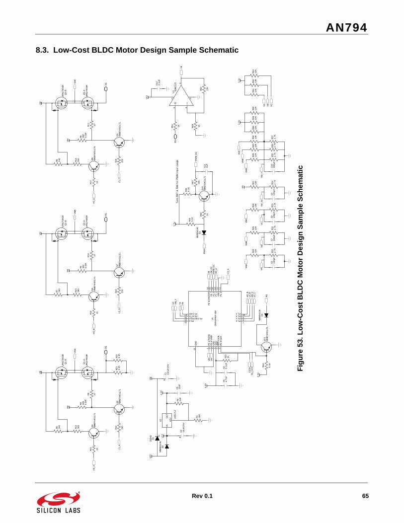
AN794
Rev 0.1 65
8.3. Low-Cost BLDC Motor Design Sample Schematic
Tune
R47
& R
48 for
PW
M in
put
rang
e
INAD
JOUT
U2
LM31
7LZ
Q1-
AUPA
2790
GR
Q1-
BUPA
2790
GR
R1 390
Q4
MM
BT44
01LT
1
D1
SS54
B
D2
MM
SD41
48
+C1 10
0uF/
25V
R2 240
R3 390
0.5W
R21
0.05
R22
0.05
R6 240
R12
360
R15
1K
R9 27
Q5
MM
BT44
01LT
1
R18
200
Q2-
AUPA
2790
GR
Q2-
BUPA
2790
GR
Q6
MM
BT44
01LT
1
R4 390
0.5W
R7 240
R13
360
R16
1K
R10
27
Q7
MM
BT44
01LT
1
R19
200
Q3-
AUPA
2790
GR
Q3-
BUPA
2790
GR
Q8
MM
BT44
01LT
1
R5 390
0.5W
R8 240
R14
360
R17
1K
R11
27
Q9
MM
BT44
01LT
1
R20
200
+C2 10
uF/2
5V
C3 10UF
1P0
.1/A
GND
2P0
.0/V
REF
3GND
4VD
D5
RST/
C2CK
6P2
.0/C
2D
7P1.6 8P1.5 9P1.4 10P1.3
11P1
.212
GND
13P1
.114
P1.0
15P0
.716
P0.6
/CNVS
TR17 P0.5/RX18 P0.4/TX19 P0.3/EXTCLK20 P0.2
21GND
U1
C805
1F85
X-GM
C4 0.1U
FC5 4.
7UF
R23
2K
R24
12K
R25
12K
R26
12K
R31
2.7K
R32
2.7K
R27
12K
R28
12K
R29
12K
R30
12K
C6 100p
FC7 10
0pF
C8 100p
FC9 10
0pF
R33
2.7K
R34
2.7K
R35
2.7K
C10
100p
FR3
62.
7KR3
72.
7K
R38
12K
R39
12K
R40
12K
R41
12K
R42
12K
R43
12K
Q10
MM
BT44
01LT
1
R48
1K
R45
5.1K
D3
MM
SD41
48
C11
1UF
R46
5.1K
R47
20K
Q11
MM
BT44
01LT
1
R44
5.1K
D4
MM
SD41
48
5 4
1
2 3
U3 N
JM21
25C12
0.1U
F
R50
10K
R51
1K R49
1K
VMA
VM
VM
RS
HS_
A
LS_A
VCC
VM
VMB
VM
RS
HS_
B
LS_B
VM
VMC
VM
RS
HS_
C
LS_C
VM
3.3V
3.3V
VMA
VMB
VMC
VM
VAVB
VCVM
_DC
VM_Y
VMA
VMB
VMC
3.3V
3.3V
VA VB VC
HS_
A
LS_A
HS_
BLS
_BHS_
CLS
_C
VM_Y
TX RXVC
VB VAVM
_DC
3.3V
PWM
PWM
_DC
PWM
_DC
3.3V
FG
FG_C
2DC2
CK
V12
V12
IM
RS
IM
Fig
ure
53.L
ow
-Co
st B
LD
C M
oto
r D
esig
n S
amp
le S
chem
atic
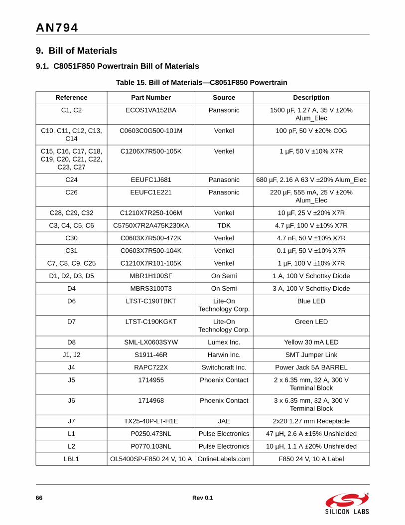
AN794
66 Rev 0.1
9. Bill of Materials
9.1. C8051F850 Powertrain Bill of Materials
Table 15. Bill of Materials—C8051F850 Powertrain
Reference Part Number Source Description
C1, C2 ECOS1VA152BA Panasonic 1500 µF, 1.27 A, 35 V ±20% Alum_Elec
C10, C11, C12, C13, C14
C0603C0G500-101M Venkel 100 pF, 50 V ±20% C0G
C15, C16, C17, C18, C19, C20, C21, C22,
C23, C27
C1206X7R500-105K Venkel 1 µF, 50 V ±10% X7R
C24 EEUFC1J681 Panasonic 680 µF, 2.16 A 63 V ±20% Alum_Elec
C26 EEUFC1E221 Panasonic 220 µF, 555 mA, 25 V ±20% Alum_Elec
C28, C29, C32 C1210X7R250-106M Venkel 10 µF, 25 V ±20% X7R
C3, C4, C5, C6 C5750X7R2A475K230KA TDK 4.7 µF, 100 V ±10% X7R
C30 C0603X7R500-472K Venkel 4.7 nF, 50 V ±10% X7R
C31 C0603X7R500-104K Venkel 0.1 µF, 50 V ±10% X7R
C7, C8, C9, C25 C1210X7R101-105K Venkel 1 µF, 100 V ±10% X7R
D1, D2, D3, D5 MBR1H100SF On Semi 1 A, 100 V Schottky Diode
D4 MBRS3100T3 On Semi 3 A, 100 V Schottky Diode
D6 LTST-C190TBKT Lite-On Technology Corp.
Blue LED
D7 LTST-C190KGKT Lite-On Technology Corp.
Green LED
D8 SML-LX0603SYW Lumex Inc. Yellow 30 mA LED
J1, J2 S1911-46R Harwin Inc. SMT Jumper Link
J4 RAPC722X Switchcraft Inc. Power Jack 5A BARREL
J5 1714955 Phoenix Contact 2 x 6.35 mm, 32 A, 300 VTerminal Block
J6 1714968 Phoenix Contact 3 x 6.35 mm, 32 A, 300 VTerminal Block
J7 TX25-40P-LT-H1E JAE 2x20 1.27 mm Receptacle
L1 P0250.473NL Pulse Electronics 47 µH, 2.6 A ±15% Unshielded
L2 P0770.103NL Pulse Electronics 10 µH, 1.1 A ±20% Unshielded
LBL1 OL5400SP-F850 24 V, 10 A OnlineLabels.com F850 24 V, 10 A Label
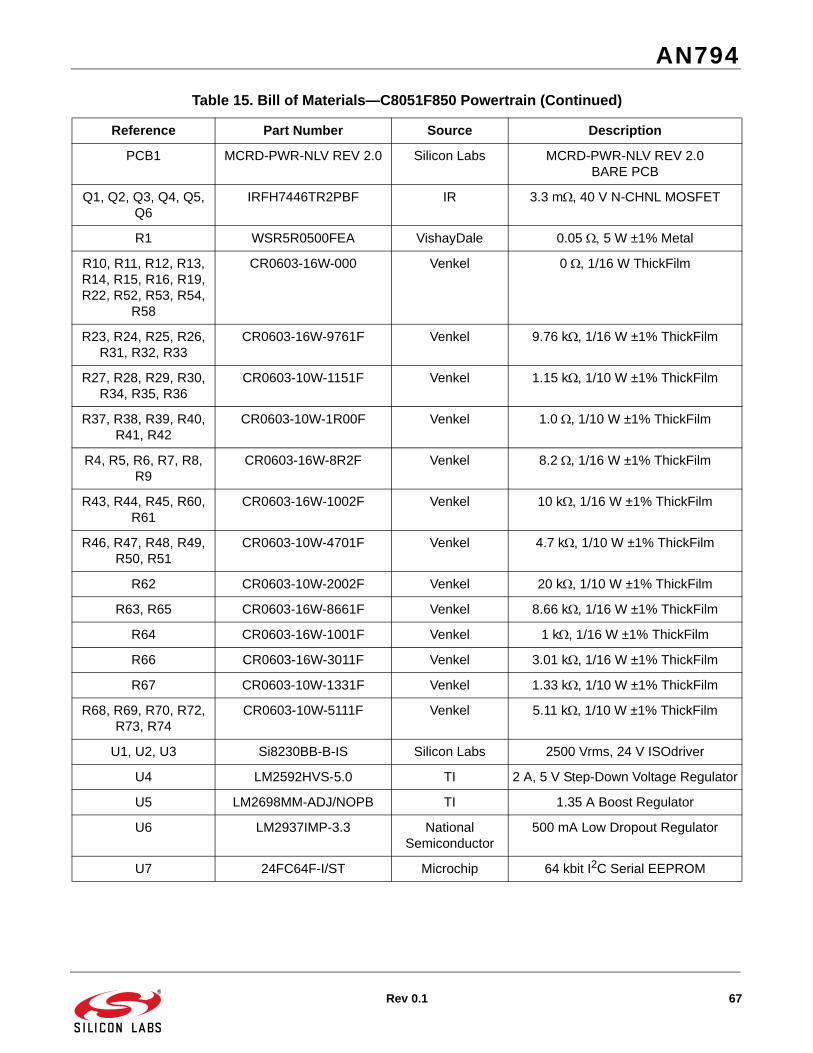
AN794
Rev 0.1 67
PCB1 MCRD-PWR-NLV REV 2.0 Silicon Labs MCRD-PWR-NLV REV 2.0 BARE PCB
Q1, Q2, Q3, Q4, Q5, Q6
IRFH7446TR2PBF IR 3.3 m, 40 V N-CHNL MOSFET
R1 WSR5R0500FEA VishayDale 0.05 5 W ±1% Metal
R10, R11, R12, R13, R14, R15, R16, R19, R22, R52, R53, R54,
R58
CR0603-16W-000 Venkel 0 , 1/16 W ThickFilm
R23, R24, R25, R26, R31, R32, R33
CR0603-16W-9761F Venkel 9.76 k, 1/16 W ±1% ThickFilm
R27, R28, R29, R30, R34, R35, R36
CR0603-10W-1151F Venkel 1.15 k, 1/10 W ±1% ThickFilm
R37, R38, R39, R40, R41, R42
CR0603-10W-1R00F Venkel 1.0 , 1/10 W ±1% ThickFilm
R4, R5, R6, R7, R8, R9
CR0603-16W-8R2F Venkel 8.2 , 1/16 W ±1% ThickFilm
R43, R44, R45, R60, R61
CR0603-16W-1002F Venkel 10 k, 1/16 W ±1% ThickFilm
R46, R47, R48, R49, R50, R51
CR0603-10W-4701F Venkel 4.7 k, 1/10 W ±1% ThickFilm
R62 CR0603-10W-2002F Venkel 20 k, 1/10 W ±1% ThickFilm
R63, R65 CR0603-16W-8661F Venkel 8.66 k, 1/16 W ±1% ThickFilm
R64 CR0603-16W-1001F Venkel 1 k, 1/16 W ±1% ThickFilm
R66 CR0603-16W-3011F Venkel 3.01 k, 1/16 W ±1% ThickFilm
R67 CR0603-10W-1331F Venkel 1.33 k, 1/10 W ±1% ThickFilm
R68, R69, R70, R72, R73, R74
CR0603-10W-5111F Venkel 5.11 k, 1/10 W ±1% ThickFilm
U1, U2, U3 Si8230BB-B-IS Silicon Labs 2500 Vrms, 24 V ISOdriver
U4 LM2592HVS-5.0 TI 2 A, 5 V Step-Down Voltage Regulator
U5 LM2698MM-ADJ/NOPB TI 1.35 A Boost Regulator
U6 LM2937IMP-3.3 National Semiconductor
500 mA Low Dropout Regulator
U7 24FC64F-I/ST Microchip 64 kbit I2C Serial EEPROM
Table 15. Bill of Materials—C8051F850 Powertrain (Continued)
Reference Part Number Source Description
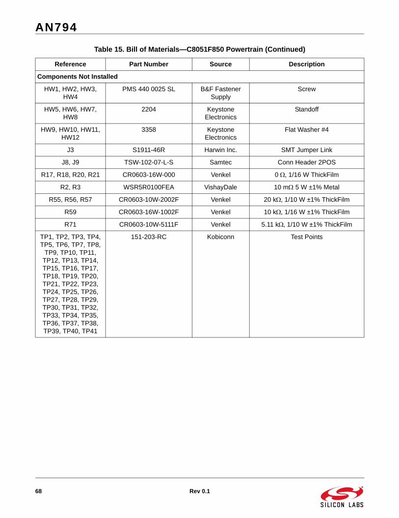
AN794
68 Rev 0.1
Components Not Installed
HW1, HW2, HW3, HW4
PMS 440 0025 SL B&F Fastener Supply
Screw
HW5, HW6, HW7, HW8
2204 Keystone Electronics
Standoff
HW9, HW10, HW11, HW12
3358 Keystone Electronics
Flat Washer #4
J3 S1911-46R Harwin Inc. SMT Jumper Link
J8, J9 TSW-102-07-L-S Samtec Conn Header 2POS
R17, R18, R20, R21 CR0603-16W-000 Venkel 0 , 1/16 W ThickFilm
R2, R3 WSR5R0100FEA VishayDale 10 m 5 W ±1% Metal
R55, R56, R57 CR0603-10W-2002F Venkel 20 k, 1/10 W ±1% ThickFilm
R59 CR0603-16W-1002F Venkel 10 k, 1/16 W ±1% ThickFilm
R71 CR0603-10W-5111F Venkel 5.11 k, 1/10 W ±1% ThickFilm
TP1, TP2, TP3, TP4, TP5, TP6, TP7, TP8,
TP9, TP10, TP11, TP12, TP13, TP14, TP15, TP16, TP17, TP18, TP19, TP20, TP21, TP22, TP23, TP24, TP25, TP26, TP27, TP28, TP29, TP30, TP31, TP32, TP33, TP34, TP35, TP36, TP37, TP38, TP39, TP40, TP41
151-203-RC Kobiconn Test Points
Table 15. Bill of Materials—C8051F850 Powertrain (Continued)
Reference Part Number Source Description
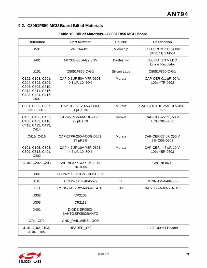
AN794
Rev 0.1 69
9.2. C8051F850 MCU Board Bill of Materials
Table 16. Bill of Materials—C8051F850 MCU Board
Reference Part Number Source Description
U501 24FC64-I/ST Microchip IC EEPROM I2C 64 kbit(8Kx8bit) 1 Mbps
U401 AP7333-33SAG7,3.3V Diodes Inc 300 mA, 3.3 V LDO Linear Regulator
U101 C8051F850-C-GU Silicon Labs C8051F850-C-GU
C102, C103, C201, C204, C302, C304, C306, C308, C310, C312, C314, C316, C403, C404, C417,
C501
CAP-0.1UF-50V-Y7R-0603, 0.1 µF, 10–80%
Murata CAP-CER-0.1 µF, 50 V, 10%-Y7R-0603
C301, C305, C307, C311, C315
CAP-1UF-25V-X5R-0603, 1 µF,10%
Murata CAP-CER-1UF-25V-10%-X5R-0603
C405, C406, C407, C408, C409, C410, C411, C412, C413,
C414
CAP-22PF-50V-COG-0603, 22 pF,10%
Venkel CAP-CER-22 pF, 50 V, 10%-C0G-0603
C415, C416 CAP-27PF-250V-COG-0603, 27 pF,5%
Murata CAP-CER-27 pF, 250 V, 5%-C0G-0603
C101, C105, C303, C309, C313, C401,
C402
CAP-4.7UF-10V-Y5R-0603, 4.7 µF, 10–80%
Murata CAP-CER, 4.7 µF, 10 V, 10%-Y5R-0603
C104, C202, C203 CAP-NI-XXX-XXX-0603, NI, 10–80%
CAP-NI-0603
U301 CF326-SX0261GM,C8051F326
J116 CONN-1X5-640456-5 TE CONN-1x5-640456-5
J501 CONN-JAE-TX24-40R-LT-H1E JAE JAE - TX24-40R-LT-H1E
U302 CP2103
U303 CP2112
D401 DIODE-SP0503-BAHTG,SP0503BAHTG
GR1, GR2 GND_RAIL,WIRE LOOP
J101, J102, J103, J104, J105
HEADER_1X2 1 x 2 100 mil Header

AN794
70 Rev 0.1
J106, J107, J108, J109, J110, J111, J112,
J113, J403
HEADER_1X3 1 x 3 100 mil Header
J115 HEADER_1X4 1 x 4 100 mil Header
U201 LMV842MM/NOPB TI IC OpAmp Dual RRIO MSOP8
MH501, MH502, MH503, MH504
MH-125 Mechanical Hole 125
D301, D305, D306, D307
OPTO-LED-GREEN-CLR-0603, GREEN
Lite-On OPTO-LED-GREEN-CLR-0603
D101, D102, D103, D302, D303, D304,
D402
OPTO-LED-RED-CLR-0603, RED
Lite-On OPTO-LED-RED-CLR-0603
R109 POT-10K-THUMBWHEEL-LIN-EAR, 10 k, 20%
Alpha (Taiwan) POT-10 kThumbwheel Linear 30 mW, 20% RoHS
R101, R501, R502, R503, R507, R508,
R509
RES-0-1%-0.1W-0603, 0 k,1% Yageo RES-0 , 1/10 W, 1%, 0603
R403 RES-1.5K-1%-0.1W-0603, 1.5 k, 1%
Venkel RES-1.5 k1/10W, 1%, 0603
R107, R108, R131, R202, R404, R405,
R406
RES-10K-1%-0.1W-0603,10 k, 1%
Yageo RES-10 k1/10W, 1%, 0603
R416, R417, R418, R419, R420, R421,
R422, R423
RES-15K-1%-0.1W-0603, 15 k, 1%
Yageo RES-15 k1/10W, 1%, 0603
R301, R302 RES-1K-1%-0.1W-0603, 1 k, 1%
Panasonic RES-1 k1/10 W, 1%, 0603
R425 RES-1M-1%-0.1W-0603, 1 M, 1%
Venkel RES-1 M, 1/10 W, 1%, 0603
R401, R402, R407, R408, R409, R410, R411, R413, R414,
R415
RES-27.4-1%-0.1W-0603, 27.4 ,1%
Venkel RES-27.4 , 1/10 W, 1%, 0603
R105, R110, R112, R310, R311, R312,
R313, R424
RES-2K-1%-0.1W-0603, 2 k,1%
Yageo RES-2 k1/10 W, 1%, 0603
R208, R209 RES-3.3K-1%-0.1 W-0603, 3.3 k,1%
Yageo RES-3.3 k, 1/10 W, 1%, 0603
Table 16. Bill of Materials—C8051F850 MCU Board (Continued)
Reference Part Number Source Description
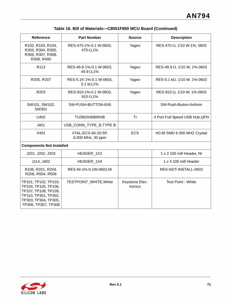
AN794
Rev 0.1 71
R102, R103, R104, R303, R304, R305, R306, R307, R308,
R309, R400
RES-470-1%-0.1 W-0603, 470 ,1%
Yageo RES-470 1/10 W-1%, 0603
R113 RES-49.9-1%-0.1 W-0603, 49.9 ,1%
Yageo RES-49.9 , 1/10 W, 1%-0603
R205, R207 RES-5.1K-1%-0.1 W-0603, 5.1 k,1%
Yageo RES-5.1 k, 1/10 W, 1%-0603
R203 RES-910-1%-0.1 W-0603, 910 ,1%
Yageo RES-910 1/10 W, 1%-0603
SW101, SW102, SW301
SW-PUSH-BUTTON-6X6 SW-Push-Button-6x6mm
U402 TUSB2046BIRHB TI 4 Port Full-Speed USB Hub,QFN
J401 USB_CONN_TYPE_B,TYPE B
X401 XTAL-ECS-60-20-5P, 6.000 MHz, 30 ppm
ECS HC49 SMD 6.000 MHZ Crystal
Components Not Installed
J201, J202, J203 HEADER_1X2 1 x 2 100 mill Header, NI
J114, J402 HEADER_1X4 1 x 4 100 mill Header
R106, R201, R204, R206, R504, R506
RES-NI-1%-0.1W-0603,NI RES-NOT-INSTALL-0603
TP101, TP102, TP103, TP104, TP105, TP106, TP107, TP108, TP109, TP110, TP301, TP302, TP303, TP304, TP305, TP306, TP307, TP308
TESTPOINT_WHITE,White Keystone Elec-tronics
Test Point - White
Table 16. Bill of Materials—C8051F850 MCU Board (Continued)
Reference Part Number Source Description

http://www.silabs.com
Silicon Laboratories Inc.400 West Cesar ChavezAustin, TX 78701USA
Simplicity Studio
One-click access to MCU and wireless tools, documentation, software, source code libraries & more. Available for Windows, Mac and Linux!
IoT Portfoliowww.silabs.com/IoT
SW/HWwww.silabs.com/simplicity
Qualitywww.silabs.com/quality
Support and Communitycommunity.silabs.com
DisclaimerSilicon Labs intends to provide customers with the latest, accurate, and in-depth documentation of all peripherals and modules available for system and software implementers using or intending to use the Silicon Labs products. Characterization data, available modules and peripherals, memory sizes and memory addresses refer to each specific device, and "Typical" parameters provided can and do vary in different applications. Application examples described herein are for illustrative purposes only. Silicon Labs reserves the right to make changes without further notice and limitation to product information, specifications, and descriptions herein, and does not give warranties as to the accuracy or completeness of the included information. Silicon Labs shall have no liability for the consequences of use of the information supplied herein. This document does not imply or express copyright licenses granted hereunder to design or fabricate any integrated circuits. The products are not designed or authorized to be used within any Life Support System without the specific written consent of Silicon Labs. A "Life Support System" is any product or system intended to support or sustain life and/or health, which, if it fails, can be reasonably expected to result in significant personal injury or death. Silicon Labs products are not designed or authorized for military applications. Silicon Labs products shall under no circumstances be used in weapons of mass destruction including (but not limited to) nuclear, biological or chemical weapons, or missiles capable of delivering such weapons.
Trademark InformationSilicon Laboratories Inc.® , Silicon Laboratories®, Silicon Labs®, SiLabs® and the Silicon Labs logo®, Bluegiga®, Bluegiga Logo®, Clockbuilder®, CMEMS®, DSPLL®, EFM®, EFM32®, EFR, Ember®, Energy Micro, Energy Micro logo and combinations thereof, "the world’s most energy friendly microcontrollers", Ember®, EZLink®, EZRadio®, EZRadioPRO®, Gecko®, ISOmodem®, Precision32®, ProSLIC®, Simplicity Studio®, SiPHY®, Telegesis, the Telegesis Logo®, USBXpress® and others are trademarks or registered trademarks of Silicon Labs. ARM, CORTEX, Cortex-M3 and THUMB are trademarks or registered trademarks of ARM Holdings. Keil is a registered trademark of ARM Limited. All other products or brand names mentioned herein are trademarks of their respective holders.