Embed Size (px)
Citation preview

Efficient Footprint Caching for Tagless DRAM Caches
Hakbeom Jang†⇤ Yongjun Lee†⇤ Jongwon Kim† Youngsok Kim‡
Jangwoo Kim‡ Jinkyu Jeong† Jae W. Lee†
†Sungkyunkwan University, Suwon, Korea ‡POSTECH, Pohang, Korea{hakbeom, yongjunlee, kimjongwon, jinkyu, jaewlee}@skku.edu {elixir, jangwoo}@postech.ac.kr
ABSTRACTEfficient cache tag management is a primary design objec-tive for large, in-package DRAM caches. Recently, TaglessDRAM Caches (TDCs) have been proposed to completelyeliminate tagging structures from both on-die SRAM andin-package DRAM, which are a major scalability bottle-neck for future multi-gigabyte DRAM caches. However,TDC imposes a constraint on DRAM cache block sizeto be the same as OS page size (e.g., 4KB) as it takesa unified approach to address translation and cache tagmanagement. Caching at a page granularity, or page-basedcaching, incurs significant off-package DRAM bandwidthwaste by over-fetching blocks within a page that are notactually used. Footprint caching is an effective solutionto this problem, which fetches only those blocks that willlikely be touched during the page’s lifetime in the DRAMcache, referred to as the page’s footprint.
In this paper we demonstrate TDC opens up unique op-portunities to realize efficient footprint caching with higherprediction accuracy and a lower hardware cost than theoriginal footprint caching scheme. Since there are no cachetags in TDC, the footprints of cached pages are trackedat TLB, instead of cache tag array, to incur much loweron-die storage overhead than the original design. Besides,when a cached page is evicted, its footprint will be storedin the corresponding page table entry, instead of an aux-iliary on-die structure (i.e., Footprint History Table), toprevent footprint thrashing among different pages, thusyielding higher accuracy in footprint prediction. The re-sulting design, called Footprint-augmented Tagless DRAMCache (F-TDC), significantly improves the bandwidth ef-ficiency of TDC, and hence its performance and energyefficiency. Our evaluation with 3D Through-Silicon-Via-based in-package DRAM demonstrates an average reduc-tion of off-package bandwidth by 32.0%, which, in turn,improves IPC and EDP by 17.7% and 25.4%, respectively,over the state-of-the-art TDC with no footprint caching.
1. INTRODUCTIONDie-stacked DRAM technologies have been widely em-
braced by industry as a means to overcome the long-standing “Memory Wall” problem [1]. A typical 3D formfactor stacks 4–8 DRAM dies with an optional logic dieat the bottom [2], whose capacity ranges from hundreds ofmegabytes to several gigabytes and will continue to scaleup with technology scaling [3]. Major processor vendors⇤These authors contributed equally to this work.
have announced their plans to integrate these technologiesinto their products, including Intel [4], AMD [5], IBM [6],Nvidia [7], and Xilinx [8].
There are proposals to architect this high-bandwidth in-package DRAM as large, software-transparent last-levelcaches [3, 9, 10, 11, 12, 13, 14, 15]. Compared to software-managed fast main memory they have an advantage in easydeployment without requiring any modification to the soft-ware stack. Since the cost of cache tags easily becomesprohibitive with large in-package DRAM, minimizing thisoverhead in terms of latency, storage, and energy con-sumption, is one of the main design challenges.
Recently, Tagless DRAM Caches (TDCs) [15] havebeen proposed to completely eliminate tagging structuresfrom both on-die SRAM and in-package DRAM. TDCaligns the granularity of caching with OS page size (e.g.,4KB) and replaces the two-step address translation byTLB (for virtual-to-physical address translation) and cachetag array (for physical-to-cache address translation) into asingle-step process. At TLB miss the TLB miss handlerperforms not only a page table walk but also cache blockallocation, and directly stores the virtual-to-cache addressmapping into the TLB. Since a TLB access immediatelyreturns the exact location of the requested block in thecache, cache tags are no longer maintained. By eliminat-ing the cache tags TDC achieves lowest hit latency andbest scalability with ever-increasing DRAM cache size.
However, TDC imposes a constraint on the DRAMcache block size to be the same as OS page size and suffersan over-fetching problem. Caching at a page granularityincurs significant off-package bandwidth waste by unnec-essarily fetching those blocks that are not actually used,which is a common problem of page-based caches.
Footprint caching [9, 10] is an effective solution to thisover-fetching problem for page-based caches. Both Foot-print Cache [10] and Unison Cache [9] track referencedblocks in a cached page since it is allocated. They use thisinformation to fetch only the relevant subset of the 64-byteblocks, referred to as the page’s footprint, when the pageis reallocated into the cache. Thus, they maintain a high hitrate of page-based caching while mitigating the bandwidthwaste by not fetching blocks that will not be used.
We identify several sources of inefficiency in the orig-inal footprint caching scheme [10], which can be effec-tively addressed on TDC. First, footprint thrashing can oc-cur among different pages as the footprint of an evictedpage is stored in a small Footprint History Table, whichcovers only a small fraction of the working set. Second,
978-1-4673-9211-2/16/$31.00 c�2016 IEEE237

the bit vectors for footprint tracking are stored in the cachetag array, whose storage overhead is proportional to theDRAM cache size. Finally, an in-package DRAM cachemiss is known only after the request goes through multipleon-die cache misses to yield a relatively high miss penalty.
In this paper we propose Footprint-augmented TaglessDRAM Cache (F-TDC), which synergistically combinesfootprint caching with TDC to improve its bandwidthefficiency. Exploiting unique opportunities offered byTDC, F-TDC outperforms the original footprint cachingscheme [10] by alleviating its sources of inefficiency. Sincethere are no cache tags in TDC, the footprints of cachedpages are tracked at TLB, instead of cache tag array, toreduce on-die storage overhead. Besides, when a page isevicted, its footprint will be stored in the correspondingpage table entry (PTE), instead of Footprint History Ta-ble, to prevent footprint thrashing among different pages,thus yielding higher prediction accuracy. Finally, F-TDCreduces an off-package miss penalty by identifying an off-package block miss right after a TLB access. Our evalua-tion with 3D Through-Silicon Via (TSV)-based in-packageDRAM demonstrates an average reduction of off-packagebandwidth by 32.0%, which, in turn, improves the IPC andEDP by 17.7% and 25.4%, respectively, over the state-of-the-art TDC with no footprint caching.
The main contributions of this paper are summarized asfollows:
• This paper is the first to identify unique opportunitiesin TDC, which enable efficient realization of foot-print caching with higher prediction accuracy at alower hardware cost than the original design [10].
• A Footprint-augmented Tagless DRAM Cache (F-TDC) is designed and implemented to capitalize onthese opportunities.
• Detailed evaluation of F-TDC with SPEC CPU 2006and CloudSuite is provided using a cycle-level sim-ulator to demonstrate its effectiveness in reducingbandwidth waste and improving the performance andenergy efficiency.
2. BACKGROUND AND MOTIVATION
2.1 Tagless DRAM CacheExisting DRAM caches can be classified into two cate-
gories based on the granularity of caching: block-based [3,12, 13, 14] and page-based [9, 10, 11, 15]. Block-basedDRAM caches adopt conventional cache block size (e.g.,64B) for efficient utilization of DRAM cache space andoff-package bandwidth. However, they require large stor-age for tags; assuming an 8-byte cache tag per 64-bytecache block, a 2GB DRAM cache requires 256MB stor-age just for tags. It is too expensive to place such a largeSRAM array on the processor die. Therefore, block-basedcaches often put the tags, together with cached data, intoin-package DRAM [3, 13], but only at the cost of an in-crease in hit latency, which negatively affects performance.
As an alternative, page-based DRAM caches alleviatethis problem by caching at a page granularity, typicallyranging from 1–8 KB [9, 10]. Smaller tags result in lowerstorage overhead and hit latency. Large block size oftenleads to higher cache hit rate by exploiting spatial local-ity. Besides, energy efficiency is improved by exploiting
CA3 I PTEP PA2 CA2 I PTEP PA1 CA1
NI PTEP PA0 CA0
000 PA4 VA4 000 PA3 VA3 001 CA2 VA2 001 CA1 VA1 001 CA0 VA0
CA2 VA2 CA0 VA0
Data (4KB)
Die-stacked DRAM cache
cTLB
GIPT Page Table
L1/L2 Cache
Off-
pack
age
DR
AM
PA2
Data (4KB)
VA2
CA2
Flags
On-
die
In
-pac
kage
D
RA
M
Figure 1: Organization and operations of TaglessDRAM Cache (TDC)
row buffer locality in DRAM devices. However, whilemuch lower than block-based DRAM caches, the storagerequirement for tags is still significant even for page-basedcaches with ever-increasing DRAM cache size. For exam-ple, assuming 4KB pages, an 8GB DRAM cache requireseither tens of megabytes on-die SRAM [10] or hundredsof megabytes [9] in-package DRAM storage just for tags.
Recently, Tagless DRAM Caches (TDCs) [15] havebeen proposed to completely eliminate tagging structuresfrom both on-die SRAM and in-package DRAM. Figure 1shows the organization and operations of TDC. At TLBmiss the TLB miss handler performs a page table walkto fetch the page table entry (PTE). If the PTE indicatesthat the page is currently not cached, the TLB miss han-dler allocates the page into the DRAM cache. Once thecache fill request is completed, the global inverted page ta-ble (GIPT) is updated, which maintains cache-to-physicaladdress mappings (along with a pointer to the correspond-ing PTE (PTEP)) for all cached pages. Finally, the TLBmiss handler updates both the TLB and the PTE with thenewly created virtual-to-cache address mapping, and re-turns. Thus, an access to the memory region within theTLB reach always hits in the cache with low hit latencyas a TLB access immediately returns the exact locationof the requested block in the cache, hence obviating theneeds to maintain cache tags. By consolidating two-stepaddress translation in the cache access path into a single-step process, TDC achieves lowest hit latency by saving atag-checking operation.
By completely eliminating cache tag array TDC is themost scalable caching solution known to date. However,TDC imposes a constraint on the cache block size to bealigned with OS page size (e.g., 4KB) and suffers an over-fetching problem, which is common to page-based caches.
2.2 Over-fetching Problem in TaglessDRAM Caches
Page-based caches, including Tagless DRAM Caches(TDCs), commonly have an over-fetching problem, whereunused blocks are moved on and off the package to causebandwidth and capacity wastes. Figure 2 compares thebandwidth consumption of the conventional page-basedDRAM cache running a multi-programmed workload,with an oracle cache, which fetches only those blocks thatwill be used. The results demonstrate the existence of sig-
238
0
2
4
6
8
10
12
128MB 256MB 512MB
Off-
pack
age
ba
ndw
idth
(GB
/s)
DRAM cache size
Oracle Page-based
Figure 2: Off-package bandwidth usage for oracle andpage-based caches while running a multi-programmedworkload (MIX 1 in Table 4)
0%
20%
40%
60%
80%
100%
10x 30x 50x 70x
Frac
tion
of p
ages
Input size scaling factor
> 48 blcoks 36 - 48 blocks 24 - 36 blocks 16 - 24 blocks 8 - 16 blocks < 8 blocks
blocks
Figure 3: Page access density for 2GB DRAM cachewith varying input size
nificant bandwidth bloat in the page-based DRAM cache,which is more pronounced for smaller caches due to highercache miss rate–by up to 5⇥ over the oracle cache.
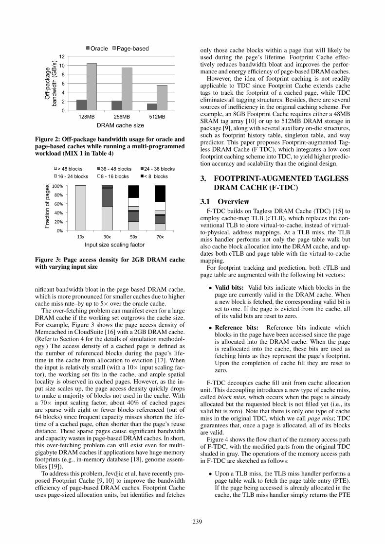
The over-fetching problem can manifest even for a largeDRAM cache if the working set outgrows the cache size.For example, Figure 3 shows the page access density ofMemcached in CloudSuite [16] with a 2GB DRAM cache.(Refer to Section 4 for the details of simulation methodol-ogy.) The access density of a cached page is defined asthe number of referenced blocks during the page’s life-time in the cache from allocation to eviction [17]. Whenthe input is relatively small (with a 10⇥ input scaling fac-tor), the working set fits in the cache, and ample spatiallocality is observed in cached pages. However, as the in-put size scales up, the page access density quickly dropsto make a majority of blocks not used in the cache. Witha 70⇥ input scaling factor, about 40% of cached pagesare sparse with eight or fewer blocks referenced (out of64 blocks) since frequent capacity misses shorten the life-time of a cached page, often shorter than the page’s reusedistance. These sparse pages cause significant bandwidthand capacity wastes in page-based DRAM caches. In short,this over-fetching problem can still exist even for multi-gigabyte DRAM caches if applications have huge memoryfootprints (e.g., in-memory database [18], genome assem-blies [19]).
To address this problem, Jevdjic et al. have recently pro-posed Footprint Cache [9, 10] to improve the bandwidthefficiency of page-based DRAM caches. Footprint Cacheuses page-sized allocation units, but identifies and fetches
only those cache blocks within a page that will likely beused during the page’s lifetime. Footprint Cache effec-tively reduces bandwidth bloat and improves the perfor-mance and energy efficiency of page-based DRAM caches.
However, the idea of footprint caching is not readilyapplicable to TDC since Footprint Cache extends cachetags to track the footprint of a cached page, while TDCeliminates all tagging structures. Besides, there are severalsources of inefficiency in the original caching scheme. Forexample, an 8GB Footprint Cache requires either a 48MBSRAM tag array [10] or up to 512MB DRAM storage inpackage [9], along with several auxiliary on-die structures,such as footprint history table, singleton table, and waypredictor. This paper proposes Footprint-augmented Tag-less DRAM Cache (F-TDC), which integrates a low-costfootprint caching scheme into TDC, to yield higher predic-tion accuracy and scalability than the original design.
3. FOOTPRINT-AUGMENTED TAGLESSDRAM CACHE (F-TDC)
3.1 OverviewF-TDC builds on Tagless DRAM Cache (TDC) [15] to
employ cache-map TLB (cTLB), which replaces the con-ventional TLB to store virtual-to-cache, instead of virtual-to-physical, address mappings. At a TLB miss, the TLBmiss handler performs not only the page table walk butalso cache block allocation into the DRAM cache, and up-dates both cTLB and page table with the virtual-to-cachemapping.
For footprint tracking and prediction, both cTLB andpage table are augmented with the following bit vectors:
• Valid bits: Valid bits indicate which blocks in thepage are currently valid in the DRAM cache. Whena new block is fetched, the corresponding valid bit isset to one. If the page is evicted from the cache, allof its valid bits are reset to zero.
• Reference bits: Reference bits indicate whichblocks in the page have been accessed since the pageis allocated into the DRAM cache. When the pageis reallocated into the cache, these bits are used asfetching hints as they represent the page’s footprint.Upon the completion of cache fill they are reset tozero.
F-TDC decouples cache fill unit from cache allocationunit. This decoupling introduces a new type of cache miss,called block miss, which occurs when the page is alreadyallocated but the requested block is not filled yet (i.e., itsvalid bit is zero). Note that there is only one type of cachemiss in the original TDC, which we call page miss; TDCguarantees that, once a page is allocated, all of its blocksare valid.
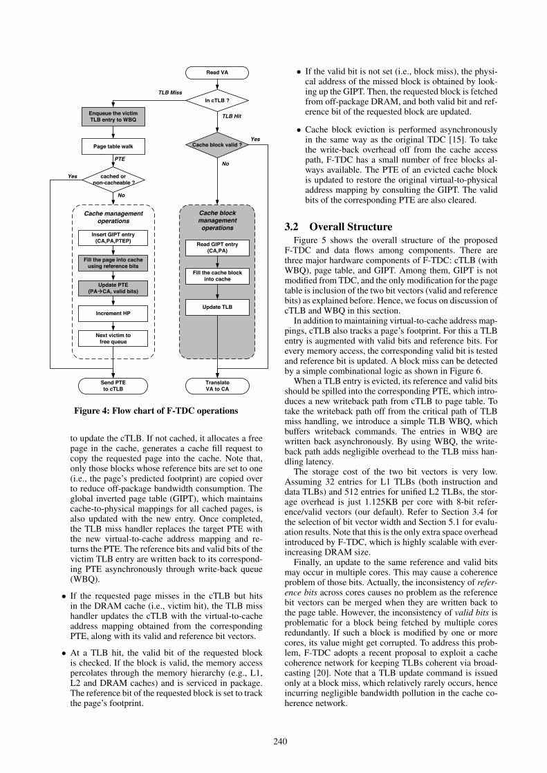
Figure 4 shows the flow chart of the memory access pathof F-TDC, with the modified parts from the original TDCshaded in gray. The operations of the memory access pathin F-TDC are sketched as follows:
• Upon a TLB miss, the TLB miss handler performs apage table walk to fetch the page table entry (PTE).If the page being accessed is already allocated in thecache, the TLB miss handler simply returns the PTE
239
In cTLB ?
Read VA
Page table walk
Send PTE to cTLB
TranslateVA to CA
TLB Miss
TLB Hit
cached or non-cacheable ?
Insert GIPT entry(CA,PA,PTEP)
Update PTE(PAàCA, valid bits)
Increment HP
Next victim to free queue
Fill the page into cache using reference bits
No
Yes
Cache managementoperations
PTE
Cache block valid ?Yes
Cache blockmanagementoperations
Update TLB
Fill the cache blockinto cache
Read GIPT entry(CA,PA)
Enqueue the victim TLB entry to WBQ
No
Figure 4: Flow chart of F-TDC operations
to update the cTLB. If not cached, it allocates a freepage in the cache, generates a cache fill request tocopy the requested page into the cache. Note that,only those blocks whose reference bits are set to one(i.e., the page’s predicted footprint) are copied overto reduce off-package bandwidth consumption. Theglobal inverted page table (GIPT), which maintainscache-to-physical mappings for all cached pages, isalso updated with the new entry. Once completed,the TLB miss handler replaces the target PTE withthe new virtual-to-cache address mapping and re-turns the PTE. The reference bits and valid bits of thevictim TLB entry are written back to its correspond-ing PTE asynchronously through write-back queue(WBQ).
• If the requested page misses in the cTLB but hitsin the DRAM cache (i.e., victim hit), the TLB misshandler updates the cTLB with the virtual-to-cacheaddress mapping obtained from the correspondingPTE, along with its valid and reference bit vectors.
• At a TLB hit, the valid bit of the requested blockis checked. If the block is valid, the memory accesspercolates through the memory hierarchy (e.g., L1,L2 and DRAM caches) and is serviced in package.The reference bit of the requested block is set to trackthe page’s footprint.
• If the valid bit is not set (i.e., block miss), the physi-cal address of the missed block is obtained by look-ing up the GIPT. Then, the requested block is fetchedfrom off-package DRAM, and both valid bit and ref-erence bit of the requested block are updated.
• Cache block eviction is performed asynchronouslyin the same way as the original TDC [15]. To takethe write-back overhead off from the cache accesspath, F-TDC has a small number of free blocks al-ways available. The PTE of an evicted cache blockis updated to restore the original virtual-to-physicaladdress mapping by consulting the GIPT. The validbits of the corresponding PTE are also cleared.
3.2 Overall StructureFigure 5 shows the overall structure of the proposed
F-TDC and data flows among components. There arethree major hardware components of F-TDC: cTLB (withWBQ), page table, and GIPT. Among them, GIPT is notmodified from TDC, and the only modification for the pagetable is inclusion of the two bit vectors (valid and referencebits) as explained before. Hence, we focus on discussion ofcTLB and WBQ in this section.
In addition to maintaining virtual-to-cache address map-pings, cTLB also tracks a page’s footprint. For this a TLBentry is augmented with valid bits and reference bits. Forevery memory access, the corresponding valid bit is testedand reference bit is updated. A block miss can be detectedby a simple combinational logic as shown in Figure 6.
When a TLB entry is evicted, its reference and valid bitsshould be spilled into the corresponding PTE, which intro-duces a new writeback path from cTLB to page table. Totake the writeback path off from the critical path of TLBmiss handling, we introduce a simple TLB WBQ, whichbuffers writeback commands. The entries in WBQ arewritten back asynchronously. By using WBQ, the write-back path adds negligible overhead to the TLB miss han-dling latency.
The storage cost of the two bit vectors is very low.Assuming 32 entries for L1 TLBs (both instruction anddata TLBs) and 512 entries for unified L2 TLBs, the stor-age overhead is just 1.125KB per core with 8-bit refer-ence/valid vectors (our default). Refer to Section 3.4 forthe selection of bit vector width and Section 5.1 for evalu-ation results. Note that this is the only extra space overheadintroduced by F-TDC, which is highly scalable with ever-increasing DRAM size.
Finally, an update to the same reference and valid bitsmay occur in multiple cores. This may cause a coherenceproblem of those bits. Actually, the inconsistency of refer-ence bits across cores causes no problem as the referencebit vectors can be merged when they are written back tothe page table. However, the inconsistency of valid bits isproblematic for a block being fetched by multiple coresredundantly. If such a block is modified by one or morecores, its value might get corrupted. To address this prob-lem, F-TDC adopts a recent proposal to exploit a cachecoherence network for keeping TLBs coherent via broad-casting [20]. Note that a TLB update command is issuedonly at a block miss, which relatively rarely occurs, henceincurring negligible bandwidth pollution in the cache co-herence network.
240

2 PTEP PA2 CA2 PTEP PA1 CA1 PTEP PA0 CA0
2
2 2 2 Valid Ref. PA3 VA3 Valid Ref. CA2 VA2 Valid Ref. CA1 VA1 Valid Ref. CA0 VA0
2 2 2
2 Valid Ref. CA1 VA1 Valid Ref. CA0 VA0
2
Valid Ref. VA3
cTLB
Page Table GIPT
L1/L2 Cache
Die-stacked DRAM cache
TLB hit but block miss
MC
WBQ
Miss
Data Block (4KB)
TLB hit and block hit
Data Block (4KB)
. . . Off-
pack
age
DR
AM
On-
die
In
-pac
kage
D
RA
M
Figure 5: The overall structure of F-TDC
CA0 10101010 10101010
Reference Valid
VA0
00010000VA0VA0
Cache
Block miss
handler
VA1VA2
cTLB
V V
Detector
Block ID(One-hot encoding)
Figure 6: Modified cTLB
3.3 F-TDC OperationsTo demonstrate the cache operations of F-TDC, we walk
through all cache access scenarios using a running exam-ple. Figure 7 depicts a snapshot of the initial state for therunning example, and Figure 8 shows the new state aftereach operation completes. The dark-shaded blocks indi-cate those components which are just updated. We use ahistory-based algorithm for footprint prediction. The refer-ence bit vector of each page records touched cache blocksduring the lifetime of the page in the DRAM cache. Whena TLB entry is evicted, its bit vector is spilled into the cor-responding PTE and used as prefetching hints at realloca-tion of the page as it represents the page’s footprint.
Case 1: TLB Miss & Cache Miss (Page Miss)Figure 8(a) depicts how F-TDC operates when a memoryaccess misses at both the cTLB and the cache. Assumingthe initial state as shown in Figure 7, a TLB access for VA2causes a TLB miss as an entry for VA2 does not exist in thecTLB ∂. To serve the TLB miss, the TLB miss handler al-locates a TLB entry for VA2. In case that cTLB is full,it evicts an existing TLB entry into WBQ (e.g., the TLBentry for VA1) ∑. WBQ later writes back the bit vectorsof the evicted TLB entry into the page table in an asyn-chronous manner. Meanwhile, the TLB page miss handlerperforms a conventional page table walk to fetch the PTEfor VA2 ∏. The fetched PTE indicates that the correspond-ing page is not currently cached (with a VA2-to-PA2 map-
0000 0110 PA4 VA4 0000 0101 PA3 VA3 0000 0011 PA2 VA2 1100 0000 CA1 VA1 1001 0000 CA0 VA0
CA3 CA2
PTEP PA1 CA1 PTEP PA0 CA0
1001 1000 CA0 VA0 1100 0100 CA1 VA1
cTLB
WBQ
GIPT Page Table
L1/L2 Cache
Die-stacked DRAM cache
Reference Valid
Reference Valid
Off-
pack
age
DR
AM
On-
die
In
-pac
kage
D
RA
M
Figure 7: Initial state of F-TDC
ping); then the TLB miss handler generates a cache fillrequest to selectively fetch the page’s footprint from off-package DRAM into the in-package DRAM cache usingthe reference bits π. Once the cache fill request is com-pleted, the TLB miss handler updates the PTE for VA2to store the VA2-to-CA2 mapping and backs up the origi-nal VA2-to-PA2 mapping at GIPT ∫. Finally, the referencebits of the page are copied over into the valid bit vector ofthe TLB entry along with the VA2-to-CA2 mapping. Thereference bit vector is cleared to track the page’s footprintduring the page’s sojourn time in the cache ª.
Case 2: TLB Hit & Cache HitWhen a memory access hits in both cTLB and the cacheas shown in Figure 8(b), F-TDC achieves the lowest ac-cess latency by requiring neither a page table walk nora TLB miss handling. As the first step, F-TDC retrievesthe TLB entry for the requested memory address fromcTLB ∂. Then, it marks the corresponding reference bitto one in cTLB and checks the corresponding valid bit ∑.The reference bit vector serves as the page’s footprint to beused when the page is reallocated. Note that both read andwrite accesses update the reference bit as reference bitstrack which blocks of a page have been accessed whilethe page resides in the cache. Once the validity of the re-quested block is confirmed, the cache address (CA2 in thisexample) is used to access the block ∏.
241

CA3 PTEP PA2 CA2 PTEP PA1 CA1 PTEP CA0 CA0
CA3 PTEP PA2 CA2 PTEP PA1 CA1 PTEP PA0 CA0
Bit vectors VA1
CA0 CA1 CA2
PTEP PTEP PTEP
PA0 PA1 PA2
CA3
TLB miss 1
Data (4KB)
Die-stacked DRAM cache
CA0 VA0 1000 1001 CA2 VA2 0001 0011
cTLB Reference Valid
WBQ
GIPT CA0 VA0 0000 1001 CA1 VA1 0100 1100
Page Table
CA2 VA2 0000 0011 PA3 VA3 0101 0000
L1/L2 Cache
VA2
Insert to WBQ 2
VA1
Page table walk 3
PA2
Data (4KB)
Allocate blocks with reference bits
4
PTE & GIPT update 5
Update TLB 6 VA2
(a) Case 1: TLB miss & cache miss (page miss)
Die-stacked DRAM
CA0 VA0 1000 1001 CA2 VA2 0011 0011
cTLB
WBQ
GIPT CA0 VA0 0000 1001 CA1 VA1 0100 1100
Page Table
CA2 VA2 0000 0011 PA3 VA3 0101
L1/L2 Cache
VA2
Data (4KB)
(b) Case 2: TLB hit & cache hit
CA2
0000
TLB hit 1 CA2
CA2
Reference bits update & check two bits
2
(c) Case 3: TLB hit & cache miss (block miss)
Die-stacked DRAM cache
CA2 VA2 0111 0111 CA1 VA1 0100 1100
cTLB
WBQ
GIPT CA0 VA0 1000 1001 CA1 VA1 0100 1100
Page Table
CA2 VA2 0000 0111 PA3 VA3 0101
L1/L2 Cache
(d) Case 4: TLB miss & cache hit (victim hit)
0000
If hit 3
Die-stacked DRAM cache
CA0 VA0 1000 1001 CA2 VA2 0111 0111
cTLB
WBQ
PTEP PTEP PTEP
GIPT CA0 VA0 0000 1001 CA1 VA1 0100 1100
Page Table
CA2 VA2 0000 0111 PA3 VA3 0101
PA0 CA0 PA1 CA1 PA2 CA2
L1/L2 Cache
VA2
Data (4KB)
0000
TLB hit 1
CA2
Reference bits update & If miss
2
Data (4KB) PA2
Allocate blocks 4
GIPT walk 3
Update valid bits 5
TLB miss 1
VA1
t
VA0 Bit vectors
VA1
2 Page table walk
Insert to WBQ 3
VA1 Update TLB 4
PA4 VA4 0110 0000 PA4 VA4 0110 0000
PA4 VA4 0110 0000 CA3 PA4 VA4 0110 0000
Reference Valid
Reference Valid
Reference Valid
Reference Valid
Reference Valid
Reference Valid
Reference Valid
0001 0010
0100 0100
Data (4KB) CA1
CA1
Figure 8: Four operations of F-TDC
Case 3: TLB Hit & Cache Miss (Block Miss)The third case, in which a memory request hits in the cTLBbut misses in the cache, can occur due to a footprint mis-prediction. Figure 8(c) shows how F-TDC handles such acase. Once a memory access to VA2 hits in the cTLB ∂,the corresponding reference bit in the TLB entry is updatedand the valid bit is checked ∑. Since the requested blockis not in the cache (i.e., valid bit is zero), the TLB misshandler looks up the GIPT to retrieve PA2, the physicaladdress of the requested page ∏. The cache fill unit usesthis address to copy the requested block into the DRAMcache π and updates the corresponding valid bit to one ∫.Then the memory request is retried to hit in the cache.
Case 4: TLB Miss & Cache Hit (Victim Hit)A victim hit occurs when a memory access misses in thecTLB but hits in the cache. This case happens as F-TDCuses the in-package DRAM region beyond the TLB reachas victim cache. Figure 8(d) illustrates the operations of F-TDC for such memory accesses. When a TLB miss occursfor VA1 ∂, the TLB miss handler performs a page tablewalk to fetch the requested PTE ∑ along with an optionaleviction of a TLB entry to WBQ ∏. Once the VA0-to-CA0mapping is restored in the cTLB π, the request is retried tohit in the cache since the requested block already resides inthe DRAM cache. Note that this process does not involveany latency penalty except for TLB miss penalty, whichmust be paid to handle the TLB miss, anyway.
In summary, Table 1 lists the four memory access op-erations in F-TDC with their latency implications. F-TDCsignificantly reduces hit latency at the cost of a slight in-crease in miss penalty for both page and block misses.
cTLB DRAM cache Descriptions
Hit Hit Cache hit.Zero latency penalty.
Hit MissBlock miss.
Costs GIPT access time andoff-package block fill time.
Miss HitIn-package victim hit.
Zero latency penalty (except forTLB miss penalty).
Miss MissOff-package cache miss.
Costs cache fill andGIPT update latency.
Table 1: Four possible cases for a memory access
3.4 Selection of Bit Vector WidthCareful selection of the width of reference and valid bits
is important because it affects the system behavior in var-ious ways. The width determines the granularity of datamovement. In F-TDC, the cache allocation unit is alignedto the OS page size (e.g., 4KB page). Hence, if the bitwidth is 8, each bit in the reference/valid bits representwhether 8 adjacent cache blocks (or 512 bytes of data)are referenced/valid in F-TDC. If more bits are used, datawill be moved at a finer granularity to mitigate the over-fetching problem at the cost of a lower hit rate. If fewerbits are used, data will be moved at a coarser granularity towaste bandwidth, but the cache hit rate will be improveddue to the spatial locality in block accesses.
Another factor affected by the bit width selection iswhether the two bit vectors can be packed in a PTE. Sinceour scheme does not maintain either SRAM tags or foot-print history table, both bit vectors should be spilled intothe PTE when a TLB entry is evicted. Wide bit vectors
242

Component ParametersCPU Out-of-order, 4 cores, 3GHzL1 TLB 32I/32D entries per coreL2 TLB 512 entries per coreL1 cache 4-way, 32KB I-cache, 32KB D-cache,
64B line, 2 cyclesL2 cache 16-way, 2MB shared cache per core,
64B line, 6 cyclesSRAM-tag Array 16-way, 256K entries
In-package DRAM (128⇠ 512MB)Bus frequency 1.6GHz (DDR 3.2GHz)Channel and Rank 1 channel, 2 ranksBank 16 banks per rankBus width 128 bits per channel
Off-package DRAM (8GB)Bus frequency 800MHz (DDR 1.6GHz)Channel and Rank 1 channel, 2 ranksBank 64 banks per rankBus width 64 bits per channel
Table 2: Architectural parameters
ParameterIn- Off-
package packageDRAM DRAM
I/O energy 2.4pJ/b 20pJ/bRD or WR energy without I/O 4pJ/b 13pJ/bACT+PRE energy (4KB page) 15nJ 15nJActivate to read delay (tRCD) 8ns 14nsRead to first data delay (tAA) 10ns 14nsActivate to precharge delay (tRAS) 22ns 35nsPrecharge command period (tRP) 14ns 14ns
Table 3: Parameters for 3D in-package DRAM and off-package DRAM devices (adapted from [22])
cannot be packed in a PTE and require additional memoryspace.
By default F-TDC uses 8 bits for each bit vector for tworeasons. First, the bit width sensitivity test reveals that it isa choice that balances prediction accuracy and bandwidthwaste (see details in Section 5.1). Second, 16 bits of bothvectors can be packed in a PTE practically. In many 64-bit CPU architectures, the width of each PTE is 64 bitsbut part of the bits are used for virtual to physical addresstranslation. For example, a recent Intel 64-bit processor [4]supports 48 bits virtual to 46 bits physical address transla-tion but each PTE is of size 64 bits. Accordingly, 18 mostsignificant bits in each PTE are unused, and 16 bits forthe valid and reference bit vectors can be packed in a PTEwithout requiring extra memory space.
4. EXPERIMENTAL SETUPWe use McSimA+ simulator [21] to evaluate the per-
formance and energy efficiency of F-TDC. Our systemmodel consists of four out-of-order CPU cores, an in-package DRAM cache, and an 8GB off-package DRAM-based main memory. The in-package DRAM cache servesas the L3 cache, which is directly connected to the CPUdie with TSV channels. Three different cache sizes areconsidered—128MB, 256MB, and 512MB. We configurethe in-package DRAM to have 4⇥ larger bandwidth thanthe off-package DDR3 DRAM. Table 2 summarizes thearchitectural parameters used for evaluation.
We extract the timing and power of the CPU coresand SRAM-based caches using McPAT [23] and those of
Name CompositionMIX1 milc, leslie3d, omnetpp, sphinx3MIX2 milc, leslie3d, soplex, omnetppMIX3 milc, soplex, GemsFDTD, omnetppMIX4 soplex, GemsFDTD, lbm, omnetppMIX5 mcf, leslie3d, lbm, sphinx3MIX6 mcf, leslie3d, GemsFDTD, omnetpp
Table 4: Composition of multi-programmed workloadsderived from SPEC CPU 2006
Application # Memory Total # MemoryAccesses Instructions Footprint
Data analytics 2 billion 29 billion 0.68GB(MapReduce)Data caching 2 billion 38 billion 2.15GB(Memcached)
Graph analytics 2 billion 23 billion 1.3GB(Tunkrank)Media Streaming 2 billion 28 billion 3.71GB
Table 5: Details of the multi-threaded workloads col-lected from CloudSuite [16]
the DRAM devices using a modified version of CACTI-3DD [24]. We adapt the parameters from recent work [22].We recompute the I/O energy for accessing memory chan-nels to be 2.4pJ/b (instead of 4pJ/b in [22]) as we re-place silicon interposers with TSV bumps. Table 3 liststhe detailed timing and power parameters used for bothin-package and off-package DRAM.
We use six multi-programmed workloads and fourmulti-threaded workloads for evaluation. To construct themulti-programmed workloads, we first collect the 11 mostmemory-intensive benchmarks from SPEC CPU 2006 bymeasuring misses per kilo instructions (MPKI). Then, foreach memory-bound benchmark, we identify the four mostrepresentative program slices using Simpoint [25], eachof which has 100 million instructions. Multi-programmedworkloads are created by randomly composing four out ofthose 11 memory-bound benchmarks. Table 4 summarizesthe six multi-programmed workloads.
For the multi-threaded workloads, we take four Cloud-Suite benchmarks with large memory footprints [16] thatrun on our simulation framework without an error. We usememory access traces [10] collected from a modified ver-sion of QEMU (Version 2.4.0) [26]. For each workload,we extract a trace of 2 billion memory reference instruc-tions after initialization to capture realistic behaviors of theworkload. The details of the four benchmarks are summa-rized in Table 5.
We compare the following three DRAM cache designs:
• Baseline Tagless DRAM Cache (TDC) models apage-based DRAM cache, which uses 4KB pages forthe unit of both allocation and cache fill. Due to datamovement at a coarse granularity, the baseline TDCsuffers significant bandwidth waste.
• Block-level Fetching without Footprint (Block-Fetching) is a simplified version of F-TDC for whicha DRAM cache block is allocated at an OS pagegranularity (i.e., 4KB) but filled at a L1/L2 cacheblock granularity (i.e., 64 bytes). Footprint cachingis disabled. This design minimizes off-package band-width waste but shows a poor DRAM cache hit ratefor not exploiting spatial locality within a page.
243
0
1
2
3
4 12
8MB
256M
B
512M
B
128M
B
256M
B
512M
B
128M
B
256M
B
512M
B
128M
B
256M
B
512M
B
128M
B
256M
B
512M
B
128M
B
256M
B
512M
B
128M
B
256M
B
512M
B
MIX1 MIX2 MIX3 MIX4 MIX5 MIX6 Average
Nor
mal
ized
IPC
Block-Fetching TDC F-TDC
0
0.5
1
1.5
128M
B
256M
B
512M
B
128M
B
256M
B
512M
B
128M
B
256M
B
512M
B
128M
B
256M
B
512M
B
128M
B
256M
B
512M
B
128M
B
256M
B
512M
B
128M
B
256M
B
512M
B
MIX1 MIX2 MIX3 MIX4 MIX5 MIX6 Average
Nor
mal
ized
ED
P
Block-Fetching TDC F-TDC
(2.7) (1.8)
Figure 9: IPC and EDP of the three cache designs. The numbers are normalized to the block-granularity cachingscheme (Block-Caching) with 128MB in-package DRAM.
• Footprint-Augmented Tagless DRAM Cache (F-TDC) is our proposed DRAM cache design. Ini-tially, F-TDC fetches all blocks for a first-touchedpage. The allocation unit (4KB) and cache fill unit(8 64-byte blocks by default) are decoupled, and thefootprint prediction and prefetching are applied. Thiscache minimizes bandwidth waste while maintaininga high cache hit rate.
5. EVALUATION
5.1 Multi-programmed WorkloadsWe first evaluate F-TDC using multi-programmed
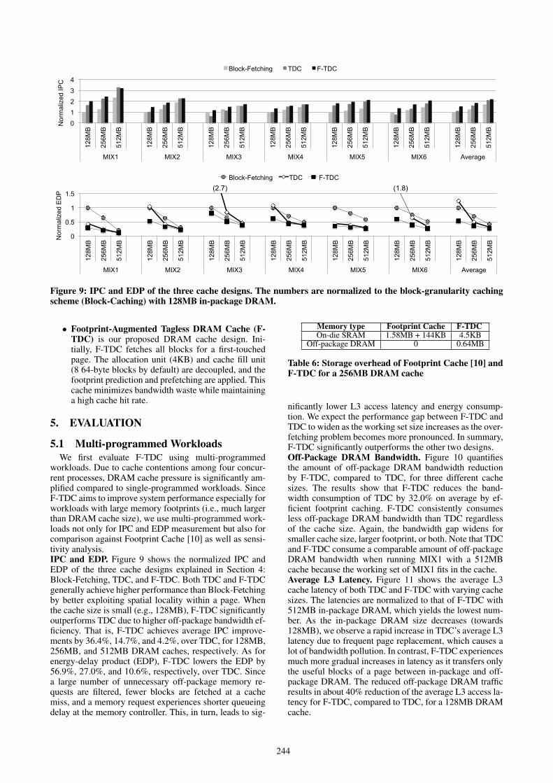
workloads. Due to cache contentions among four concur-rent processes, DRAM cache pressure is significantly am-plified compared to single-programmed workloads. SinceF-TDC aims to improve system performance especially forworkloads with large memory footprints (i.e., much largerthan DRAM cache size), we use multi-programmed work-loads not only for IPC and EDP measurement but also forcomparison against Footprint Cache [10] as well as sensi-tivity analysis.IPC and EDP. Figure 9 shows the normalized IPC andEDP of the three cache designs explained in Section 4:Block-Fetching, TDC, and F-TDC. Both TDC and F-TDCgenerally achieve higher performance than Block-Fetchingby better exploiting spatial locality within a page. Whenthe cache size is small (e.g., 128MB), F-TDC significantlyoutperforms TDC due to higher off-package bandwidth ef-ficiency. That is, F-TDC achieves average IPC improve-ments by 36.4%, 14.7%, and 4.2%, over TDC, for 128MB,256MB, and 512MB DRAM caches, respectively. As forenergy-delay product (EDP), F-TDC lowers the EDP by56.9%, 27.0%, and 10.6%, respectively, over TDC. Sincea large number of unnecessary off-package memory re-quests are filtered, fewer blocks are fetched at a cachemiss, and a memory request experiences shorter queueingdelay at the memory controller. This, in turn, leads to sig-
Memory type Footprint Cache F-TDCOn-die SRAM 1.58MB + 144KB 4.5KB
Off-package DRAM 0 0.64MB
Table 6: Storage overhead of Footprint Cache [10] andF-TDC for a 256MB DRAM cache
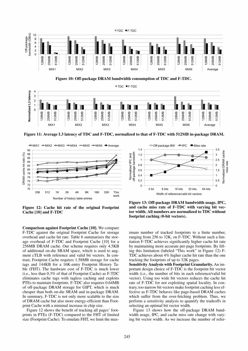
nificantly lower L3 access latency and energy consump-tion. We expect the performance gap between F-TDC andTDC to widen as the working set size increases as the over-fetching problem becomes more pronounced. In summary,F-TDC significantly outperforms the other two designs.Off-Package DRAM Bandwidth. Figure 10 quantifiesthe amount of off-package DRAM bandwidth reductionby F-TDC, compared to TDC, for three different cachesizes. The results show that F-TDC reduces the band-width consumption of TDC by 32.0% on average by ef-ficient footprint caching. F-TDC consistently consumesless off-package DRAM bandwidth than TDC regardlessof the cache size. Again, the bandwidth gap widens forsmaller cache size, larger footprint, or both. Note that TDCand F-TDC consume a comparable amount of off-packageDRAM bandwidth when running MIX1 with a 512MBcache because the working set of MIX1 fits in the cache.Average L3 Latency. Figure 11 shows the average L3cache latency of both TDC and F-TDC with varying cachesizes. The latencies are normalized to that of F-TDC with512MB in-package DRAM, which yields the lowest num-ber. As the in-package DRAM size decreases (towards128MB), we observe a rapid increase in TDC’s average L3latency due to frequent page replacement, which causes alot of bandwidth pollution. In contrast, F-TDC experiencesmuch more gradual increases in latency as it transfers onlythe useful blocks of a page between in-package and off-package DRAM. The reduced off-package DRAM trafficresults in about 40% reduction of the average L3 access la-tency for F-TDC, compared to TDC, for a 128MB DRAMcache.
244
0 2 4 6 8
10
128M
B
256M
B
512M
B
128M
B
256M
B
512M
B
128M
B
256M
B
512M
B
128M
B
256M
B
512M
B
128M
B
256M
B
512M
B
128M
B
256M
B
512M
B
128M
B
256M
B
512M
B
MIX1 MIX2 MIX3 MIX4 MIX5 MIX6 Average
Off-
pack
age
ba
ndw
idth
(GB
/s)
TDC F-TDC
Figure 10: Off-package DRAM bandwidth consumption of TDC and F-TDC.
0 1 2 3 4
128M
B
256M
B
512M
B
128M
B
256M
B
512M
B
128M
B
256M
B
512M
B
128M
B
256M
B
512M
B
128M
B
256M
B
512M
B
128M
B
256M
B
512M
B
128M
B
256M
B
512M
B
MIX1 MIX2 MIX3 MIX4 MIX5 MIX6 Average
Nor
mal
ized
L3
late
ncy
TDC F-TDC
Figure 11: Average L3 latency of TDC and F-TDC, normalized to that of F-TDC with 512MB in-package DRAM.
70 72 74 76 78 80 82 84 86 88 90
256 512 1K 2K 4K 8K 16K 32K This work
DR
AM
cac
he h
it ra
tio (%
)
Number of history table entries
MIX1 MIX2 MIX3 MIX4 MIX5 MIX6 Average
Figure 12: Cache hit rate of the original FootprintCache [10] and F-TDC
Comparison against Footprint Cache [10]. We compareF-TDC against the original Footprint Cache for storageoverhead and cache hit rate. Table 6 summarizes the stor-age overhead of F-TDC and Footprint Cache [10] for a256MB DRAM cache. Our scheme requires only 4.5KBof additional on-die SRAM space, which is used to aug-ment cTLB with reference and valid bit vectors. In con-trast, Footprint Cache requires 1.58MB storage for cachetags and 144KB for a 16K-entry Footprint History Ta-ble (FHT). The hardware cost of F-TDC is much lower(i.e., less than 0.3% of that of Footprint Cache) as F-TDCeliminates cache tags with tagless caching and exploitsPTEs to maintain footprints. F-TDC also requires 0.64MBof off-package DRAM storage for GIPT, which is muchcheaper than both on-die SRAM and in-package DRAM.In summary, F-TDC is not only more scalable to the sizeof DRAM cache but also more energy-efficient than Foot-print Cache with a minimal increase in chip size.
Figure 12 shows the benefit of tracking all pages’ foot-prints in PTEs (F-TDC) compared to the FHT of limitedsize (Footprint Cache). To emulate FHT, we limit the max-
0
0.5
1
1.5
2
2.5
3
3.5
0
0.2
0.4
0.6
0.8
1
1.2
1.4
0 bit 8 bits 16 bits 32 bits 64 bits
Nor
mal
ized
DR
AM
cac
he
mis
s ra
te
Nor
mal
ized
IPC
and
of
f-pac
kage
ban
dwid
th
Width of reference/valid bit vectors
Off-package BW IPC Miss rate
Figure 13: Off-package DRAM bandwidth usage, IPC,and cache miss rate of F-TDC with varying bit vec-tor width. All numbers are normalized to TDC withoutfootprint caching (0-bit vectors).
imum number of tracked footprints to a finite number,ranging from 256 to 32K, on F-TDC. Without such a lim-itation F-TDC achieves significantly higher cache hit rateby maintaining more accurate per-page footprints. By lift-ing this limitation (labeled “This work” in Figure 12) F-TDC achieves about 4% higher cache hit rate than the onetracking the footprints of up to 32K pages.Sensitivity Analysis with Footprint Granularity. An im-portant design choice of F-TDC is the footprint bit vectorwidth (i.e., the number of bits in each reference/valid bitvector). Using too wide bit vectors reduces the cache hitrate of F-TDC for not exploiting spatial locality. In con-trary, too narrow bit vectors make footprint caching less ef-fective as F-TDC behaves like page-based DRAM cacheswhich suffer from the over-fetching problem. Thus, weperform a sensitivity analysis to quantify the tradeoffs inselecting an optimal bit vector width.
Figure 13 shows how the off-package DRAM band-width usage, IPC, and cache miss rate change with vary-ing bit vector width. As we increase the number of refer-
245
0 1 2 3 4 5
128M
B
256M
B
512M
B
128M
B
256M
B
512M
B
128M
B
256M
B
512M
B
128M
B
256M
B
512M
B
128M
B
256M
B
512M
B
Data analytics
Data caching
Graph analytics
Media streaming
Average
Nor
mal
ized
L3
late
ncy
TDC F-TDC
Figure 14: Average L3 latency of TDC and F-TDCwith multi-threaded workloads, normalized to that ofF-TDC with 512MB in-package DRAM.
ence and valid bits, we observe an increase in the cachemiss rate and a decrease in the off-package DRAM band-width usage. This means that we can control the bit vec-tor width to find a sweet spot between block-based caches(with wide bit vectors) and page-based caches (with nar-row bit vectors) to take the best of both. Our evaluationdemonstrates that the highest IPC improvement of 18.7%is achieved with 8-bit vectors for both reference and validbits. Therefore, we choose the width of 8 bits as default.
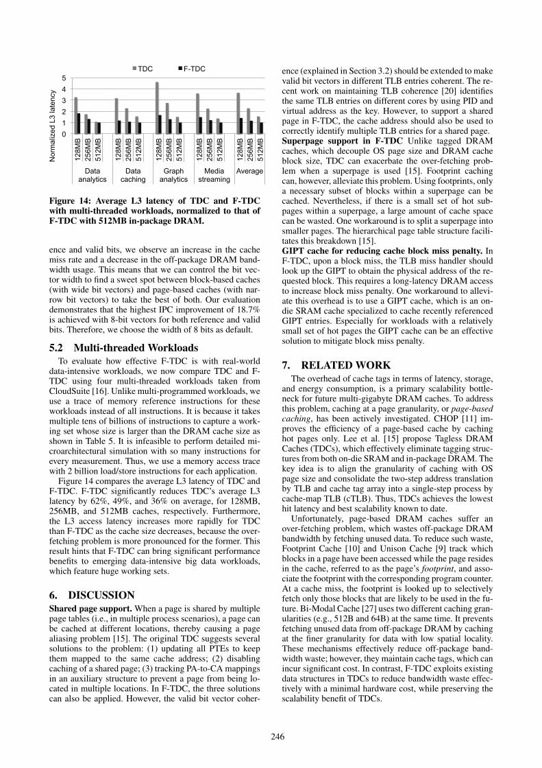
5.2 Multi-threaded WorkloadsTo evaluate how effective F-TDC is with real-world
data-intensive workloads, we now compare TDC and F-TDC using four multi-threaded workloads taken fromCloudSuite [16]. Unlike multi-programmed workloads, weuse a trace of memory reference instructions for theseworkloads instead of all instructions. It is because it takesmultiple tens of billions of instructions to capture a work-ing set whose size is larger than the DRAM cache size asshown in Table 5. It is infeasible to perform detailed mi-croarchitectural simulation with so many instructions forevery measurement. Thus, we use a memory access tracewith 2 billion load/store instructions for each application.
Figure 14 compares the average L3 latency of TDC andF-TDC. F-TDC significantly reduces TDC’s average L3latency by 62%, 49%, and 36% on average, for 128MB,256MB, and 512MB caches, respectively. Furthermore,the L3 access latency increases more rapidly for TDCthan F-TDC as the cache size decreases, because the over-fetching problem is more pronounced for the former. Thisresult hints that F-TDC can bring significant performancebenefits to emerging data-intensive big data workloads,which feature huge working sets.
6. DISCUSSIONShared page support. When a page is shared by multiplepage tables (i.e., in multiple process scenarios), a page canbe cached at different locations, thereby causing a pagealiasing problem [15]. The original TDC suggests severalsolutions to the problem: (1) updating all PTEs to keepthem mapped to the same cache address; (2) disablingcaching of a shared page; (3) tracking PA-to-CA mappingsin an auxiliary structure to prevent a page from being lo-cated in multiple locations. In F-TDC, the three solutionscan also be applied. However, the valid bit vector coher-
ence (explained in Section 3.2) should be extended to makevalid bit vectors in different TLB entries coherent. The re-cent work on maintaining TLB coherence [20] identifiesthe same TLB entries on different cores by using PID andvirtual address as the key. However, to support a sharedpage in F-TDC, the cache address should also be used tocorrectly identify multiple TLB entries for a shared page.Superpage support in F-TDC Unlike tagged DRAMcaches, which decouple OS page size and DRAM cacheblock size, TDC can exacerbate the over-fetching prob-lem when a superpage is used [15]. Footprint cachingcan, however, alleviate this problem. Using footprints, onlya necessary subset of blocks within a superpage can becached. Nevertheless, if there is a small set of hot sub-pages within a superpage, a large amount of cache spacecan be wasted. One workaround is to split a superpage intosmaller pages. The hierarchical page table structure facili-tates this breakdown [15].GIPT cache for reducing cache block miss penalty. InF-TDC, upon a block miss, the TLB miss handler shouldlook up the GIPT to obtain the physical address of the re-quested block. This requires a long-latency DRAM accessto increase block miss penalty. One workaround to allevi-ate this overhead is to use a GIPT cache, which is an on-die SRAM cache specialized to cache recently referencedGIPT entries. Especially for workloads with a relativelysmall set of hot pages the GIPT cache can be an effectivesolution to mitigate block miss penalty.
7. RELATED WORKThe overhead of cache tags in terms of latency, storage,
and energy consumption, is a primary scalability bottle-neck for future multi-gigabyte DRAM caches. To addressthis problem, caching at a page granularity, or page-basedcaching, has been actively investigated. CHOP [11] im-proves the efficiency of a page-based cache by cachinghot pages only. Lee et al. [15] propose Tagless DRAMCaches (TDCs), which effectively eliminate tagging struc-tures from both on-die SRAM and in-package DRAM. Thekey idea is to align the granularity of caching with OSpage size and consolidate the two-step address translationby TLB and cache tag array into a single-step process bycache-map TLB (cTLB). Thus, TDCs achieves the lowesthit latency and best scalability known to date.
Unfortunately, page-based DRAM caches suffer anover-fetching problem, which wastes off-package DRAMbandwidth by fetching unused data. To reduce such waste,Footprint Cache [10] and Unison Cache [9] track whichblocks in a page have been accessed while the page residesin the cache, referred to as the page’s footprint, and asso-ciate the footprint with the corresponding program counter.At a cache miss, the footprint is looked up to selectivelyfetch only those blocks that are likely to be used in the fu-ture. Bi-Modal Cache [27] uses two different caching gran-ularities (e.g., 512B and 64B) at the same time. It preventsfetching unused data from off-package DRAM by cachingat the finer granularity for data with low spatial locality.These mechanisms effectively reduce off-package band-width waste; however, they maintain cache tags, which canincur significant cost. In contrast, F-TDC exploits existingdata structures in TDCs to reduce bandwidth waste effec-tively with a minimal hardware cost, while preserving thescalability benefit of TDCs.
246

Recently, extended TLB (eTLB) has been proposed forTagLess Cache (TLC) [28] and Direct-to-Data (D2D) [29]cache, which keep way index for cached blocks in a TLB.Similar to F-TDC a TLB lookup returns the exact loca-tion of the requested block in the cache. However, bothtarget conventional on-die L1/L2 caches and do not ad-dress unique design challenges or leverage opportunitieswith die-stacked DRAM caches.
Alternatives to page-based DRAM caches includeblock-based DRAM caches [12, 14]. Although free ofthe over-fetching problem, block-based caches have muchgreater overhead with cache tags due to their fine-grainedcaching, and reducing this overhead is the primary designobjective for them. Loh-Hill Cache [3] stores both tagsand cache blocks in the same DRAM row, making a sin-gle row buffer open sufficient to serve both a tag accessand the subsequent block access. Sim et al. [30] reducethe implementation cost of Loh-Hill Cache by introduc-ing a multi-level cache hit/miss predictor. Like Loh-HillCache, Alloy Cache [13] also stores tags and their blocksin the same DRAM row, but collocates a tag and the cor-responding block to further reduce the cost of a tag-and-block access to be a single-burst latency. ATCache [31]aims to accelerate tag accesses by employing an SRAM-based tag cache, which caches recently-accessed tags. Un-fortunately, the inherent tagging overhead of block-basedDRAM caches easily becomes a scalability bottleneck forfuture multi-gigabyte DRAM caches.
Chou et al. find that even block-based DRAM cachessuffer from significant DRAM bandwidth pollution fromsecondary cache operations (other than tag and dataaccesses, or the primary operations) [32]. To dedicatemore bandwidth to these primary operations, they pro-pose Bandwidth Efficient ARchitecture (BEAR), whichreduces the bandwidth consumption of cache fills, write-back probes, and miss probes. While BEAR focuses onachieving higher in-package DRAM bandwidth efficiency,F-TDC aims to minimize off-package DRAM bandwidthwaste via efficient footprint caching.
There are proposals to use in-package DRAM not ascaches but as part-of-memory to expand the main memorysize. In such cases, it is important to efficiently migratedata between fast-but-small in-package DRAM and large-but-slow off-package DRAM as the placement of data canhas significant impact on performance. Sim et al. [33]propose a hardware-only approach, which introduces an-other level of address translation from physical addressesinto DRAM addresses. This approach does not require OSmodifications as the hardware swaps OS pages betweenthe fast and slow DRAM under the hood. In contrast,Meswani et al. [34] propose a hardware/software coopera-tive approach, which migrates hot OS pages. They extendTLB to measure a page’s hotness and make OS not onlydetermine the page’s placement using this information butalso perform page migrations if necessary. Chou et al. [35]propose to use in-package DRAM as both a DRAM cacheand part-of-memory by migrating data between in-packageand off-package DRAMs upon a cache miss.
8. CONCLUSIONThis paper introduces Footprint-augmented Tagless
DRAM Cache (F-TDC), which synergistically inte-grates footprint caching into the Tagless DRAM Cache
(TDC) [15]. Exploiting unique opportunities offered byTDC, F-TDC realizes efficient footprint caching withhigher prediction accuracy at a lower hardware cost thanthe state-of-the-art footprint caches [9,10]. Our evaluationwith 3D TSV-based in-package DRAM demonstrates thatF-TDC effectively reduces the off-package DRAM band-width, and thus significantly improves performance andenergy efficiency, while retaining the scalability benefit ofthe original TDC.
9. ACKNOWLEDGMENTSThis research was supported by Basic Science Re-
search Program through the National Research Founda-tion of Korea (NRF) funded by the Ministry of Science,ICT & Future Planning (NRF-2014R1A1A1005894 andNRF-2014R1A1A1003746) and the Ministry of Education(NRF-2014R1A1A2054658).
10. REFERENCES[1] W. A. Wulf and S. A. McKee, “Hitting the Memory Wall:
Implications of the Obvious,” ACM SIGARCH ComputerArchitecture News, vol. 23, no. 1, 1995.
[2] J. T. Pawlowski, “Hybrid Memory Cube (HMC),” in Hot Chips 23,2011.
[3] G. H. Loh and M. D. Hill, “Efficiently Enabling ConventionalBlock Sizes for Very Large Die-stacked DRAM Caches,” in Proc.44th Annual IEEE/ACM International Symposium onMicroarchitecture (MICRO), 2011.
[4] S. Anthony, “Intel unveils 72-core x86 Knights Landing CPU forexascale supercomputing.”http://www.extremetech.com/extreme/171678-intel-unveils-72-core-x86-knights-landing.
[5] H. Mujtaba, “AMD Working With Hynix For Development ofHigh-Bandwidth 3D Stacked Memory.”http://wccftech.com/amd-working-hynix-development-highbandwidth-3d-stacked-memory/.
[6] S. S. Iyer, “The Evolution of Dense Embedded Memory in HighPerformance Logic Technologies,” in Proc. 2012 IEEEInternational Electron Devices Meeting (IEDM), 2012.
[7] “Nvidia to stack up DRAM on future ’Volta’ GPUs.”http://www.theregister.co.uk/2013/03/19/nvidia_gpu_roadmap_computing_update/.
[8] S. Lakka, “Xilinx SSI Technology: Concept to SiliconDevelopment Overview.” http://www.hotchips.org/wp-content/uploads/hc_archives/hc24/HC24-Tut2-Die-Stack/HC24.27.240-Overview-Lakka-Xilink.pdf.
[9] D. Jevdjic, G. H. Loh, C. Kaynak, and B. Falsafi, “Unison Cache:A Scalable and Effective Die-Stacked DRAM Cache,” in Proc.47th Annual IEEE/ACM International Symposium onMicroarchitecture (MICRO), 2014.
[10] D. Jevdjic, S. Volos, and B. Falsafi, “Die-Stacked DRAM Cachesfor Servers: Hit Ratio, Latency, or Bandwidth? Have It All withFootprint Cache,” in Proc. 40th Annual International Symposiumon Computer Architecture (ISCA), 2013.
[11] X. Jiang, N. Madan, L. Zhao, M. Upton, R. Iyer, S. Makineni,D. Newell, Y. Solihin, and R. Balasubramonian, “CHOP: AdaptiveFilter-Based DRAM Caching for CMP Server Platforms,” in Proc.16th International Symposium on High Performance ComputerArchitecture (HPCA), 2010.
[12] G. H. Loh, “Extending the Effectiveness of 3D-Stacked DRAMCaches with an Adaptive Multi-Queue Policy,” in Proc. 42ndAnnual IEEE/ACM International Symposium on Microarchitecture(MICRO), 2009.
[13] M. K. Qureshi and G. H. Loh, “Fundamental Latency Trade-offs inArchitecting DRAM Caches: Outperforming ImpracticalSRAM-Tags with a Simple and Practical Design,” in Proc. 45thAnnual IEEE/ACM International Symposium on Microarchitecture(MICRO), 2012.
[14] L. Zhao, R. Iyer, R. Illikkal, and D. Newell, “Exploring DRAMCache Architectures for CMP Server Platforms,” in Proc. 25thInternational Conference on Computer Design (ICCD), 2007.
247
[15] Y. Lee, J. Kim, H. Jang, H. Yang, J. Kim, J. Jeong, and J. W. Lee,“A Fully Associative, Tagless DRAM Cache,” in Proc. 42ndAnnual International Symposium on Computer Architecture(ISCA), 2015.
[16] “CloudSuite benchmark 2.0.”http://parsa.epfl.ch/cloudsuite.
[17] S. Volos, J. Picorel, B. Falsafi, and B. Grot, “Bump: Bulk memoryaccess prediction and streaming,” in Proc. 47th Annual IEEE/ACMInternational Symposium on Microarchitecture (MICRO), 2014.
[18] “SAP HANA In-Memory Platform.” http://go.sap.com/solution/in-memory-platform.html.
[19] S. L. Salzberg, A. M. Phillippy, A. Zimin, D. Puiu, T. Magoc,S. Koren, T. J. Treangen, M. C. Schatz, A. L. Delcher, M. Roberts,G. Marçais, M. Pop, and J. A. Yorke, “GAGE: A critical evaluationof genome assemblies and assembly algorithms,” GenomeResearch, vol. 22, no. 6, 2012.
[20] V. Seshadri, G. Pekhimenko, O. Ruwase, O. Mutlu, P. B. Gibbons,M. A. Kozuch, T. C. Mowry, and T. Chilimbi, “Page Overlays: AnEnhanced Virtual Memory Framework to Enable Fine-grainedMemory Management,” in Proc. 42nd Annual InternationalSymposium on Computer Architecture (ISCA), 2015.
[21] J. H. Ahn, S. Li, S. O, and N. P. Jouppi, “McSimA+: A ManycoreSimulator with Application-level+ Simulation and DetailedMicroarchitecture Modeling,” in Proc. IEEE InternationalSymposium on Performance Analysis of Systems and Software(ISPASS), 2013.
[22] Y. H. Son, S. O, H. Yang, D. Jung, J. H. Ahn, J. Kim, J. Kim, andJ. W. Lee, “Microbank: Architecting Through-SiliconInterposer-Based Main Memory Systems,” in Proc. InternationalConference for High Performance Computing, Networking,Storage and Analysis (SC), 2014.
[23] S. Li, J. H. Ahn, R. D. Strong, J. B. Brockman, D. M. Tullsen, andN. P. Jouppi, “McPAT: An Integrated Power, Area, and TimingModeling Framework for Multicore and Manycore Architectures,”in Proc. 42nd Annual IEEE/ACM International Symposium onMicroarchitecture (MICRO), 2009.
[24] K. Chen, S. Li, N. Muralimanohar, J. H. Ahn, J. B. Brockman, andN. P. Jouppi, “CACTI-3DD: Architecture-level Modeling for 3DDie-stacked DRAM Main Memory,” in Proc. Design, Automation& Test in Europe Conference & Exhibition (DATE), 2012.
[25] T. Sherwood, E. Perelman, G. Hamerly, and B. Calder,“Automatically Characterizing Large Scale Program Behavior,” in
Proc. 10th International Conference on Architectural Support forProgramming Languages and Operating Systems (ASPLOS), 2002.
[26] F. Bellard, “Qemu open source processor emulator,” URL:http://www. qemu. org, 2007.
[27] N. Gulur, M. Mehendale, R. Manikantan, and R. Govindarajan,“Bi-Modal DRAM Cache: Improving Hit Rate, Hit Latency andBandwidth,” in Proc. 47th International Symposium onMicroarchitecture (MICRO), 2014.
[28] A. Sembrant, E. Hagersten, and D. Black-Shaffer, “Tlc: A tag-lesscache for reducing dynamic first level cache energy,” in Proc. 46thAnnual IEEE/ACM International Symposium on Microarchitecture(MICRO), 2013.
[29] A. Sembrant, E. Hagersten, and D. Black-Schaffer, “Thedirect-to-data (d2d) cache: Navigating the cache hierarchy with asingle lookup,” in Proc. 41st Annual International Symposium onComputer Architecture, 2014.
[30] J. Sim, G. H. Loh, H. Kim, M. O’Connor, and M. Thottethodi, “AMostly-Clean DRAM Cache for Effective Hit Speculation andSelf-Balancing Dispatch,” in Proc. 45th Annual IEEE/ACMInternational Symposium on Microarchitecture (MICRO), 2012.
[31] C.-C. Huang and V. Nagarajan, “ATCache: Reducing DRAMCache Latency via a Small SRAM Tag Cache,” in Proc. 23rdInternational Conference on Parallel Architectures andCompilation Techniques (PACT), 2014.
[32] C. Chou, A. Jaleel, and M. K. Qureshi, “BEAR: Techniques forMitigating Bandwidth Bloat in Gigascale DRAM Caches,” inProc. 42nd International Symposium on Computer Architecture(ISCA), 2015.
[33] J. Sim, A. R. Alameldeen, Z. Chishti, C. Wilkerson, and H. Kim,“Transparent Hardware Management of Stacked DRAM as Part ofMemory,” in Proc. 47th International Symposium onMicroarchitecture (MICRO), 2014.
[34] M. R. Meswani, S. Blagodurov, D. Roberts, J. Slice,M. Ignatowski, and G. H. Loh, “Heterogeneous MemoryArchitectures: A HW/SW Approach for Mixing Die-stacked andOff-package Memories,” in Proc. 21st International Symposium onHigh Performance Computer Architecture (HPCA), 2015.
[35] C. Chou, A. Jaleel, and M. K. Qureshi, “CAMEO:A Two-LevelMemory Organization with Capacity of Main Memory andFlexibility of Hardware-Managed Cache,” in Proc. 47thInternational Symposium on Microarchitecture (MICRO), 2014.
248