Embed Size (px)
Citation preview
전도성 고분자의 이해 및 응용
Conducting/semiconducting
polymers in organic electronics
Organic Electronic Devices
김 철 암한국전자통신연구원 기반 기술연구소
유기전자소자팀
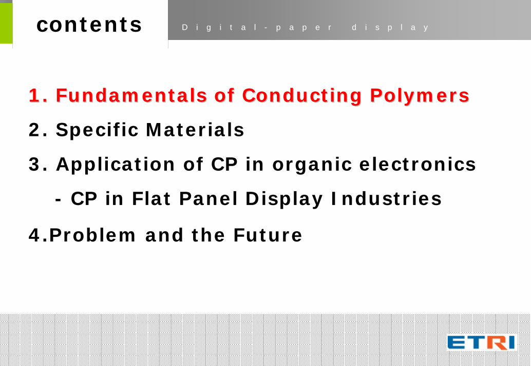
D i g i t a l - p a p e r d i s p l a y contents
1.1. Fundamentals of Conducting PolymersFundamentals of Conducting Polymers
2. Specific Materials
3. Application of CP in organic electronics
- CP in Flat Panel Display Industries
4.Problem and the Future
Conjugated polymers
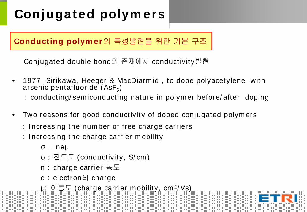
• 1977 Sirikawa, Heeger & MacDiarmid , to dope polyacetylene with arsenic pentafluoride (AsF5): conducting/semiconducting nature in polymer before/after doping
• Two reasons for good conductivity of doped conjugated polymers
: Increasing the number of free charge carriers: Increasing the charge carrier mobility
σ = neμ
σ : 전도도 (conductivity, S/cm)n : charge carrier 농도
e : electron의 chargeμ: 이동도 )charge carrier mobility, cm2/Vs)
Conducting polymer의 특성발현을 위한 기본 구조
Conjugated double bond의 존재에서 conductivity발현
Conjugated polymers
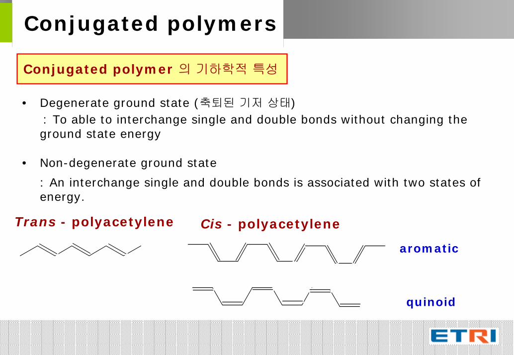
• Degenerate ground state (축퇴된 기저 상태) : To able to interchange single and double bonds without changing the ground state energy
• Non-degenerate ground state
: An interchange single and double bonds is associated with two states of energy.
Conjugated polymer 의 기하학적 특성
Trans - polyacetylene Cis - polyacetylene
aromatic
quinoid
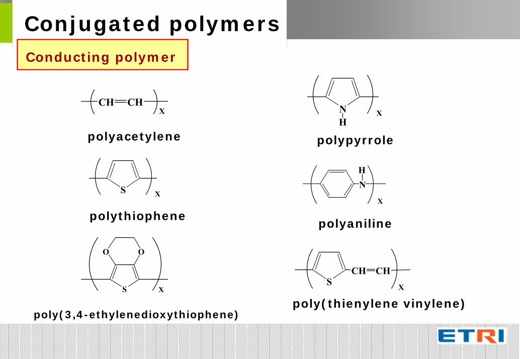
Conjugated polymersConducting polymer
CH CHX
S X
S
O O
X
N XH
S X
CH CH
N
X
H
polyacetylene
polythiophene
poly(3,4-ethylenedioxythiophene)
polypyrrole
poly(thienylene vinylene)
polyaniline
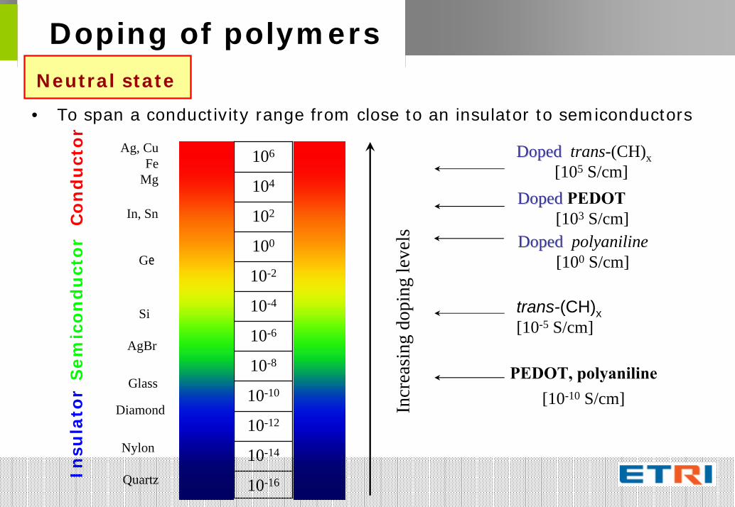
Doping of polymersNeutral state
• To span a conductivity range from close to an insulator to semiconductors
106
104
102
100
10-2
10-4
10-6
10-8
10-10
10-12
10-14
10-16
Co
nd
uct
or
Ag, CuFe
Mg
DopedDoped trans-(CH)x[105 S/cm]
DopedDoped PEDOT[103 S/cm]In, Sn
Incr
easi
ng d
opin
g le
vels
Ge
Si
AgBr
Glass
Diamond
Nylon
Quartz
trans-(CH)x[10-5 S/cm]
DopedDoped polyaniline[100 S/cm]
Sem
ico
nd
uct
or
PEDOT, polyaniline[10-10 S/cm]
Insu
lato
r
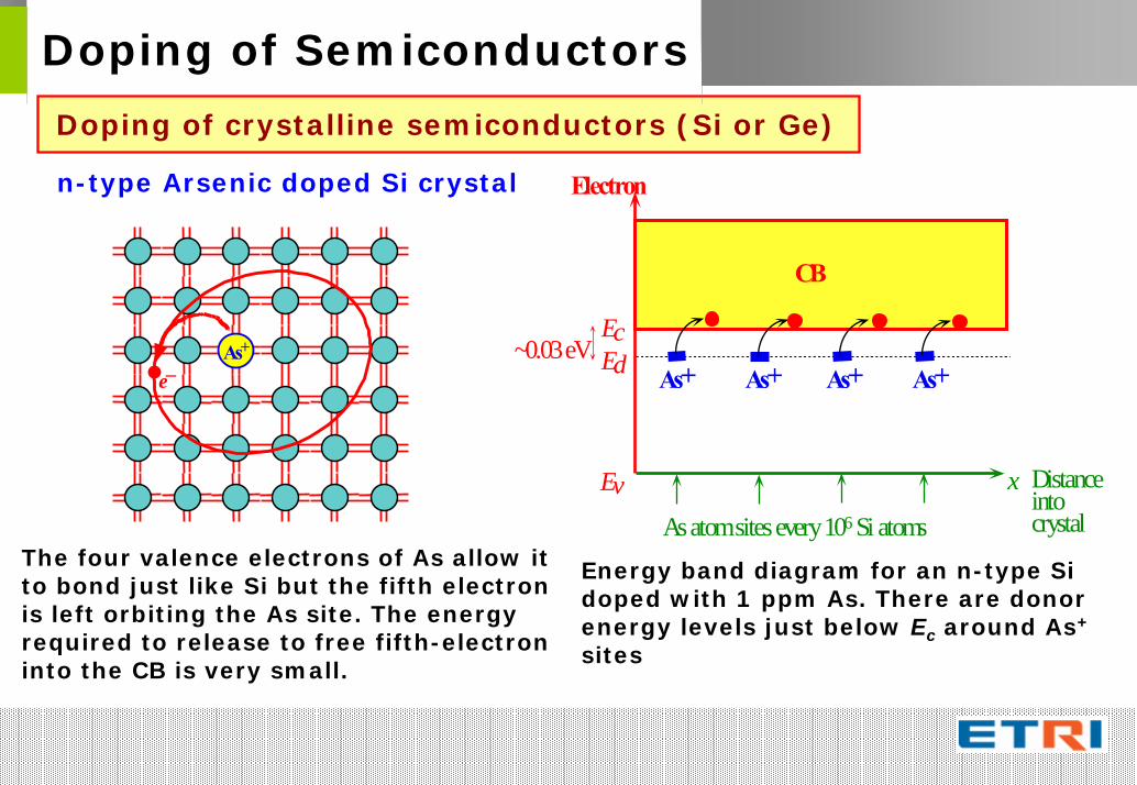
Doping of Semiconductors
Doping of crystalline semiconductors (Si or Ge)
As+
e–
n-type Arsenic doped Si crystal
The four valence electrons of As allow it to bond just like Si but the fifth electron is left orbiting the As site. The energy required to release to free fifth-electron into the CB is very small.
x
As+ As+ As+ As+
EcEd
EvAsatomsitesevery106 Si atoms
Distanceintocrystal
~0.03eV
CB
Electron
Energy band diagram for an n-type Sidoped with 1 ppm As. There are donor energy levels just below Ec around As+
sites
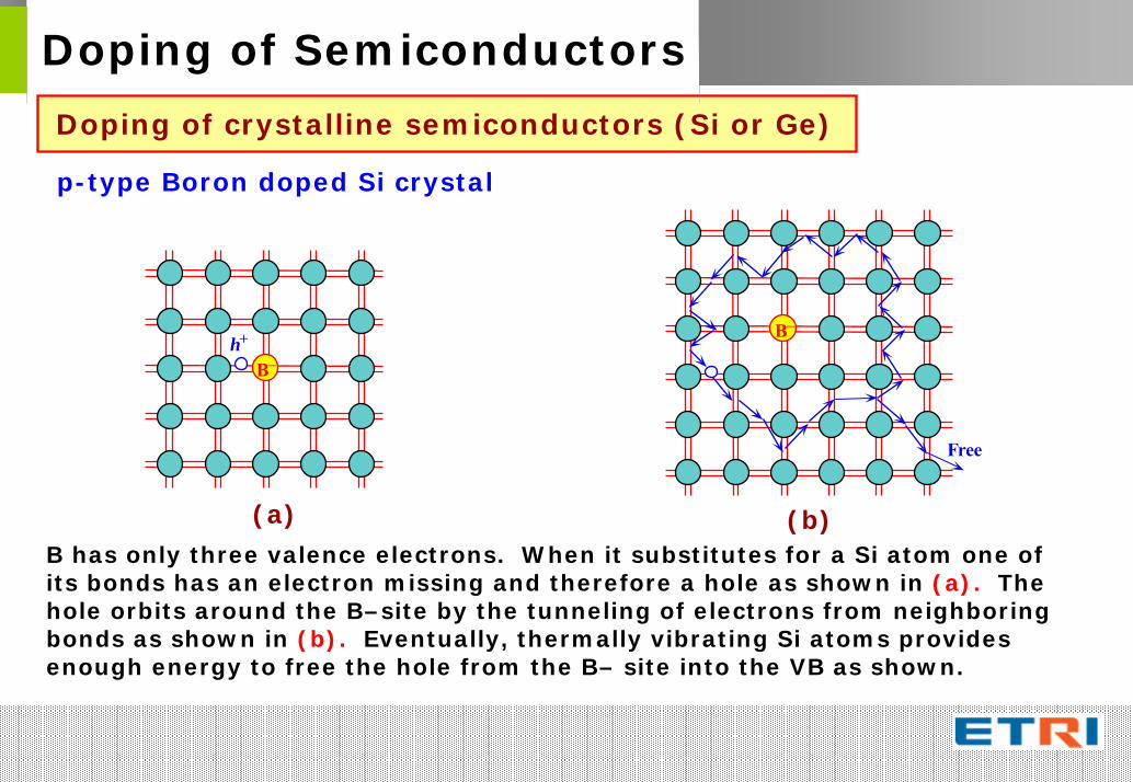
Doping of Semiconductors
Doping of crystalline semiconductors (Si or Ge)
p-type Boron doped Si crystal
B–h+
Free
B–
B has only three valence electrons. When it substitutes for a Si atom one of its bonds has an electron missing and therefore a hole as shown in (a). The hole orbits around the B–site by the tunneling of electrons from neighboring bonds as shown in (b). Eventually, thermally vibrating Si atoms provides enough energy to free the hole from the B– site into the VB as shown.
(a) (b)
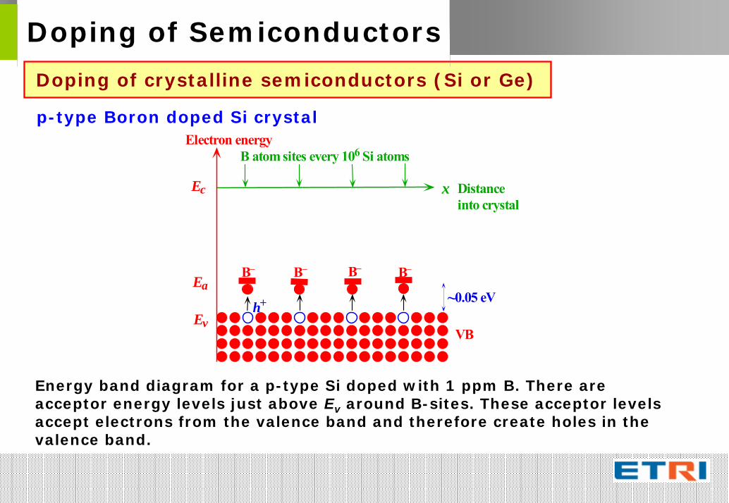
Doping of Semiconductors
Doping of crystalline semiconductors (Si or Ge)
p-type Boron doped Si crystal
x
B–
Ev
Ea
B atom sites every 106 Si atoms
Distanceinto crystal
~0.05 eV
B– B– B–
h+
VB
Ec
Electron energy
Energy band diagram for a p-type Si doped with 1 ppm B. There are acceptor energy levels just above Ev around B-sites. These acceptor levels accept electrons from the valence band and therefore create holes in the valence band.
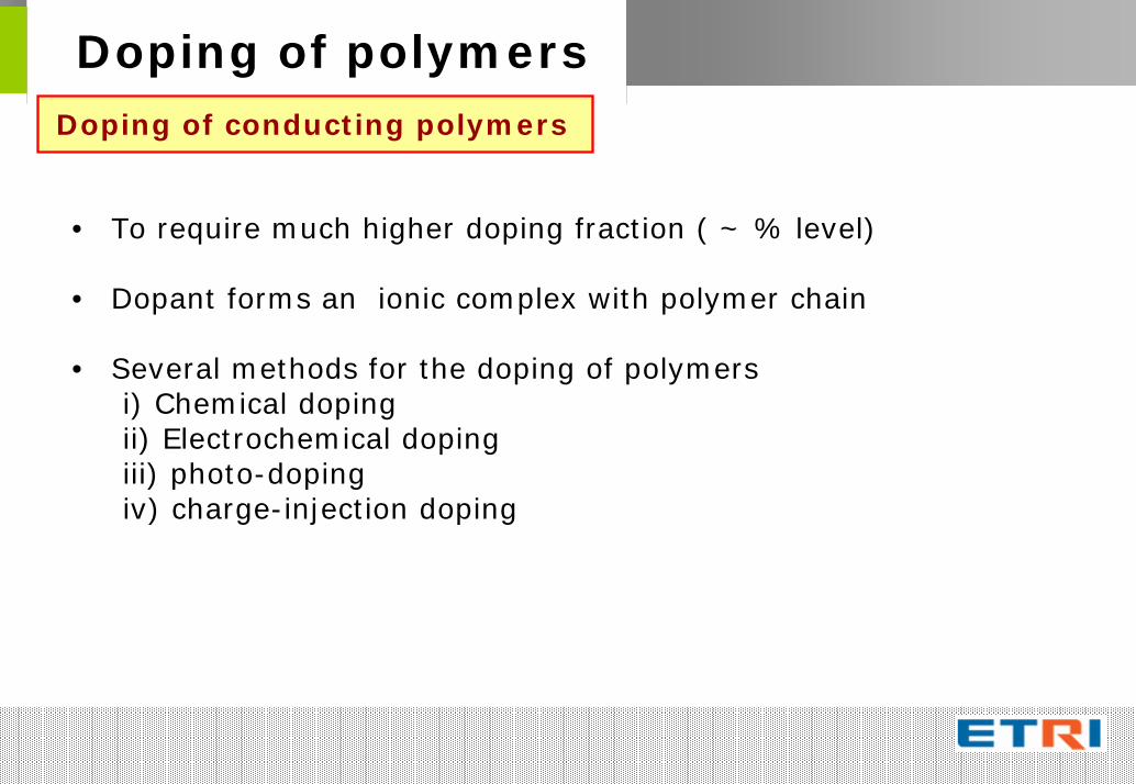
Doping of polymersDoping of conducting polymers
• To require much higher doping fraction ( ~ % level)
• Dopant forms an ionic complex with polymer chain
• Several methods for the doping of polymersi) Chemical dopingii) Electrochemical dopingiii) photo-dopingiv) charge-injection doping
Doping of polymers
−−+− +⇔+ yeAPyAP yy
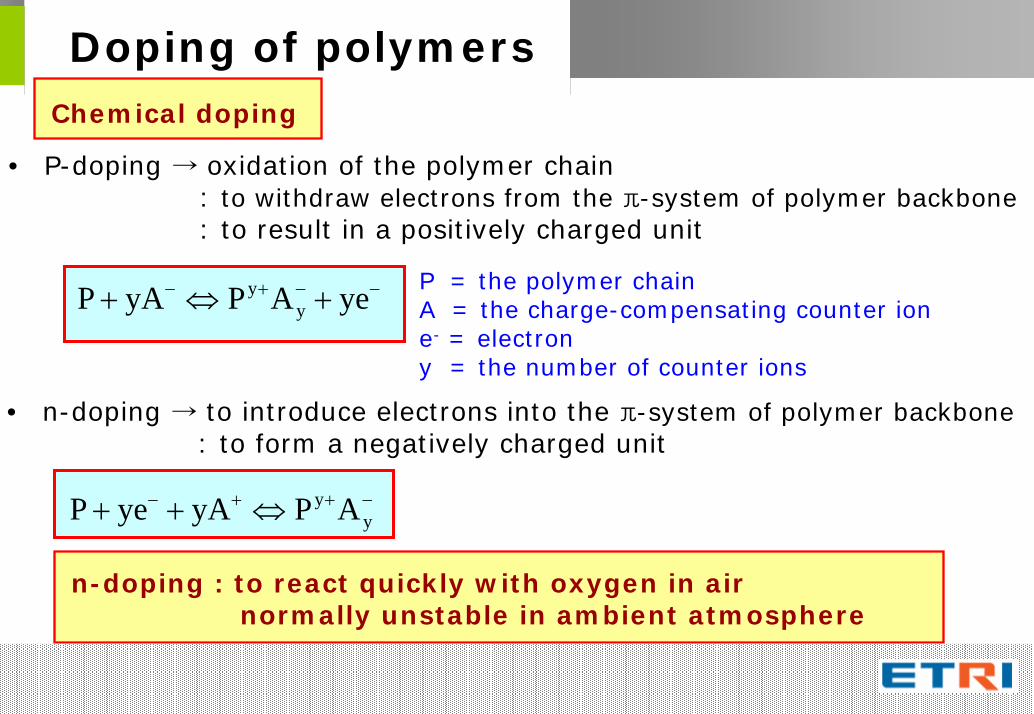
Chemical doping
• P-doping → oxidation of the polymer chain: to withdraw electrons from the π-system of polymer backbone: to result in a positively charged unit
• n-doping → to introduce electrons into the π-system of polymer backbone: to form a negatively charged unit
−++− ⇔++ yy APyAyeP
P = the polymer chainA = the charge-compensating counter ione- = electrony = the number of counter ions
n-doping : to react quickly with oxygen in airnormally unstable in ambient atmosphere
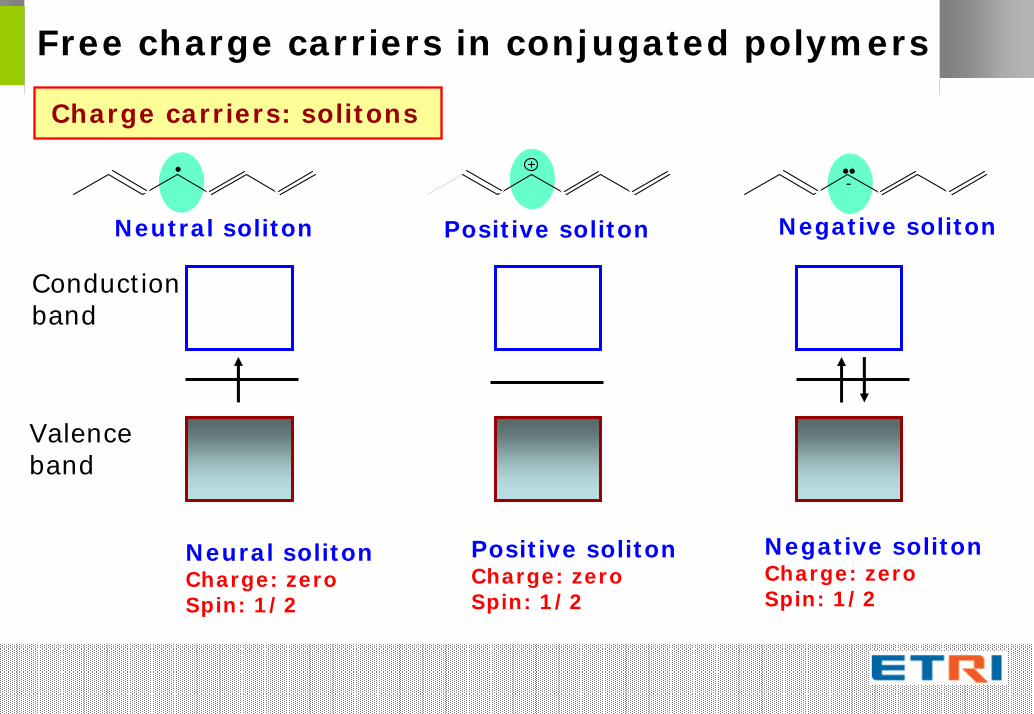
Free charge carriers in conjugated polymers
Charge carriers: solitons
Conduction band
-
Neutral soliton Negative solitonPositive soliton
Valence band
Negative solitonCharge: zeroSpin: 1/2
Positive solitonCharge: zeroSpin: 1/2
Neural solitonCharge: zeroSpin: 1/2
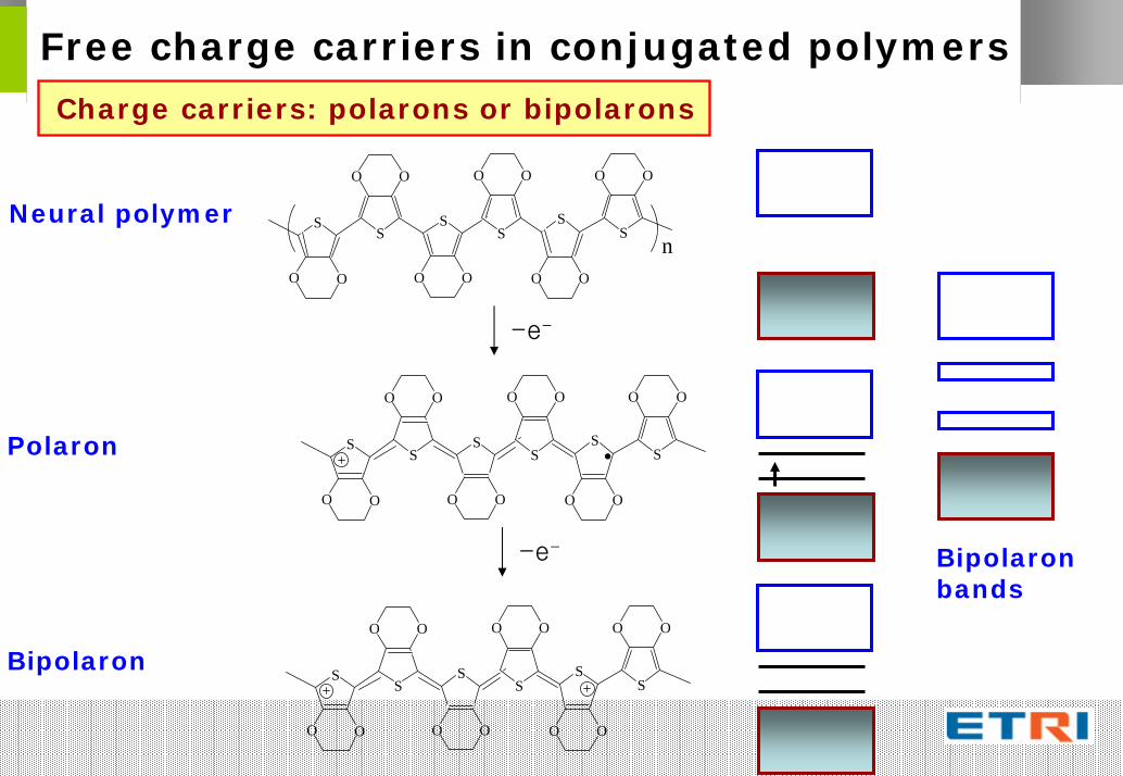
Free charge carriers in conjugated polymersCharge carriers: polarons or bipolarons
S
OO
S
O O
S
OO
S
O O
S
OO
S
O O
S
OO
S
O O
S
OO
S
O O
S
OO
S
O O
n
-e-
-e-
S
OO
S
O O
S
OO
S
O O
S
OO
S
O O
Neural polymer
Bipolaron
Polaron
Bipolaronbands
Doping of conducting polymers
• The highest conductivity is associated with “mixed valence”states of fractional charges per repeat unit of polymers.
• To easily move non-charged sites to charged sites → High σ
• Measurements of potential dependence of polythiophenes, polypyrroles and polyaniline on conductivity
: For polyaniline (PANI)level of more than 0.5 electrons per repeat unit oxidised state→ to start to show a decrease in conductivity
Free charge carriers in conjugated polymers
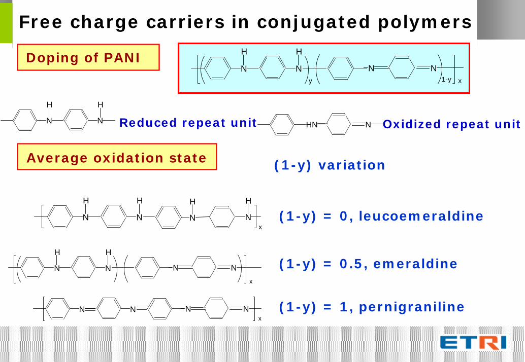
Free charge carriers in conjugated polymers
N
H
N
H
y
N N1-y x
Doping of PANI
N
H
N
H
HN NReduced repeat unit Oxidized repeat unit
Average oxidation state (1-y) variation
N
H
N
H
N N
H H
x(1-y) = 0, leucoemeraldine
N
H
N
H
N Nx
(1-y) = 0.5, emeraldine
N N N Nx
(1-y) = 1, pernigraniline
Free charge carriers in conjugated polymers
Optical state change by doping level
• Doping introduces new state in the energy band gap.– To cause the absorption to shift towards lower energies
• For typical conjugated polymers, to have a band gap of 1.7 – 3 eV– To absorb visible wavelengths of light (in neutral form)– To switch to the infrared absorption by doping
Electrochromism
• The band gap of the polymer is dependent on the structure of polymer. (to determine the conjugation length).
• A long conjugation length (large electron delocalization)– To yield a small band gap
• By introducing different side groups along the polymer– To tune the band gap– To influence solubility, thermal stability, oxidation potential….
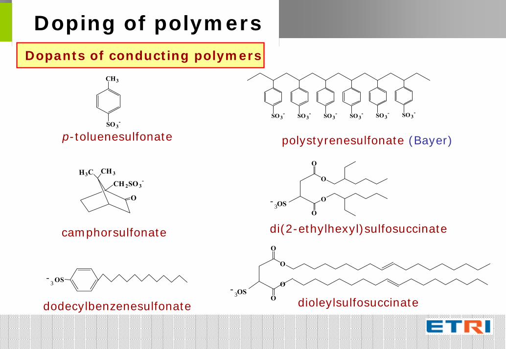
Doping of polymersDopants of conducting polymers
CH 3H3CCH 2SO3
-
O
CH3
SO3-
SO 3- SO 3
- SO 3- SO 3
- SO 3- SO 3
-
O
O
O
O3
- OS
O
O
O
O3
- OS
camphorsulfonate
p-toluenesulfonate polystyrenesulfonate (Bayer)
di(2-ethylhexyl)sulfosuccinate
dioleylsulfosuccinate
OS3-
dodecylbenzenesulfonate
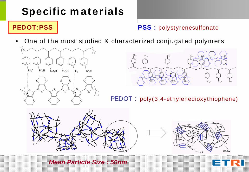
Specific materialsPEDOT:PSS
• One of the most studied & characterized conjugated polymers
PSS : polystyrenesulfonate
S
OO
S
O O
S
OO
S
O O
S
OO
S
O O
SO3- SO3H SO3H SO3H SO3
- SO3H
n
nPEDOT : poly(3,4-ethylenedioxythiophene)
Mean Particle Size : 50nm
D i g i t a l - p a p e r d i s p l a y contents
1.1. Fundamentals of Conducting PolymersFundamentals of Conducting Polymers
2.2. Specific MaterialsSpecific Materials
3. Application of CP in organic electronics
- CP in Flat Panel Display Industries
4.Problem and the Future
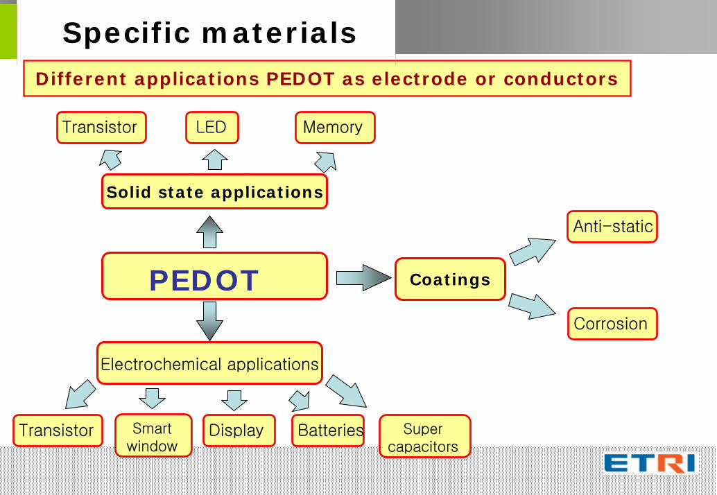
Specific materialsDifferent applications PEDOT as electrode or conductors
PEDOT
Solid state applications
Electrochemical applications
Transistor LED Memory
Transistor Smart window
Display Batteries Super capacitors
Coatings
Anti-static
Corrosion
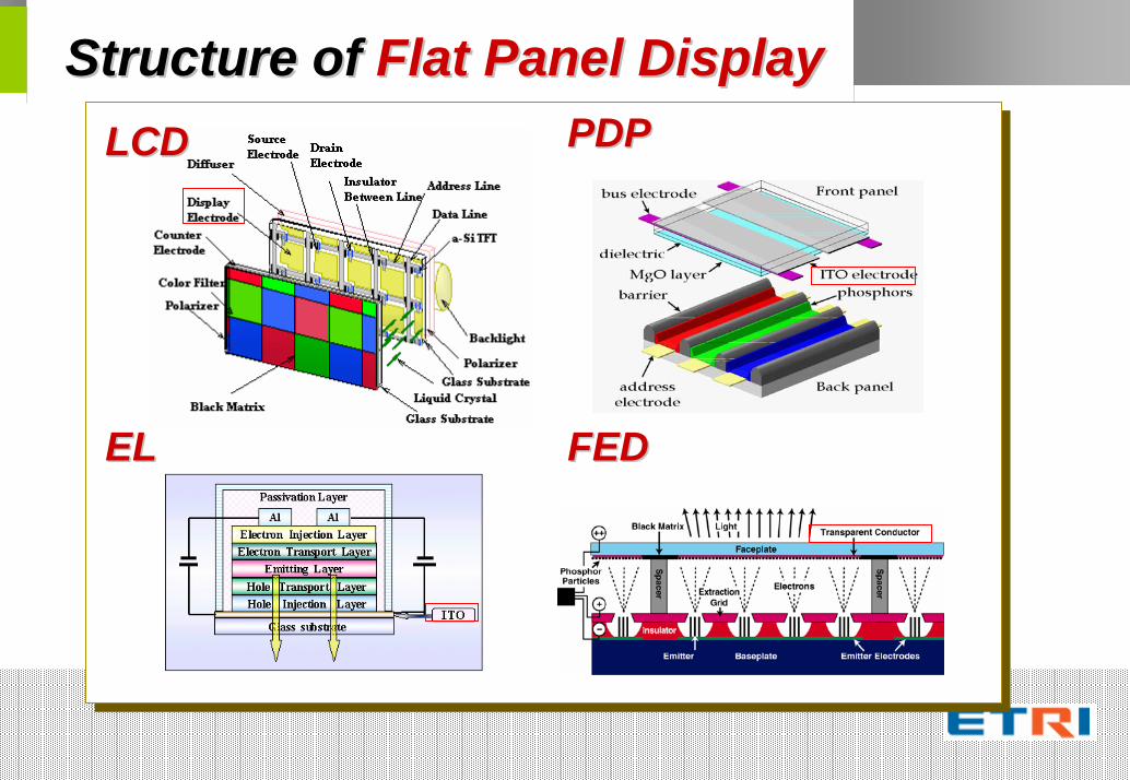
Structure of Structure of Flat Panel DisplayFlat Panel DisplayLCDLCD PDPPDP
ELEL FEDFED
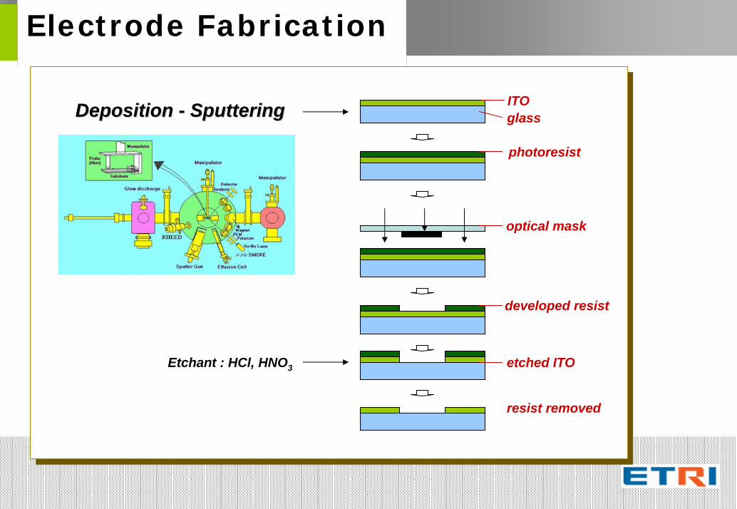
Electrode Fabrication
Deposition Deposition -- SputteringSputtering glassITO
photoresist
optical mask
developed resist
etched ITO
resist removed
Etchant : HCl, HNO3
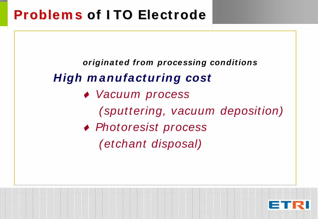
ProblemsProblems of ITO Electrodeof ITO Electrode
originated from processing conditions
High manufacturing cost ♦ Vacuum process
(sputtering, vacuum deposition)♦ Photoresist process
(etchant disposal)
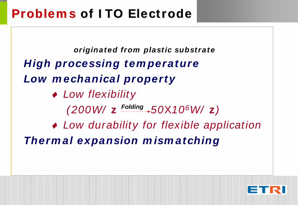
ProblemsProblems of ITO Electrodeof ITO Electrode
originated from processing conditions
High manufacturing cost ♦ Vacuum process
(sputtering, vacuum deposition)♦ Photoresist process
(etchant disposal)
originated from plastic substrate
High processing temperatureLow mechanical property
♦ Low flexibility(200W/ z 50X106W/ z)
♦ Low durability for flexible applicationThermal expansion mismatching
Folding
RequirementsRequirements of Flexible Electrodeof Flexible Electrode
High Transparency (>80%)High Conductivity (<100Ω/ )Low CostFlexible Mechanical PropertyAppropriate Thermal ExpansionPrinting & Patterning CapabilityEnvironmental Stability
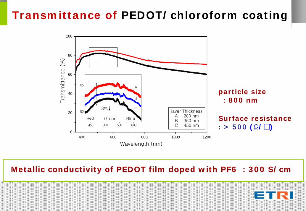
Transmittance of PEDOT/chloroform coating
400 600 800 1000 12000
20
40
60
80
100
3%
BlueGreenRed
450 500 550 600
80
85
C
B
A
layer ThicknessA 200 nmB 350 nmC 450 nm
Tra
nsm
itta
nce (
%)
Wavelength (nm)
Metallic conductivity of PEDOT film doped with PF6 : 300 S/cmMetallic conductivity of PEDOT film doped with PF6 : 300 S/cm
particle size: 800 nm
Surface resistance: > 500 (Ω/)
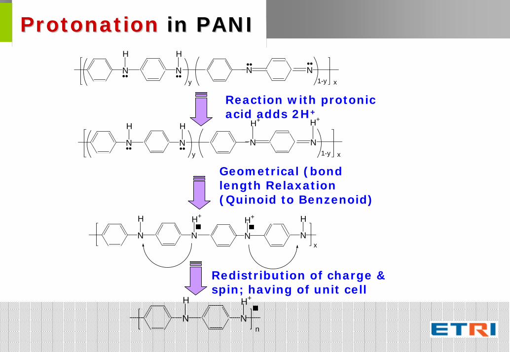
ProtonationProtonation in PANIin PANI
N
H
N
H
y
N N1-y x
N
H
N
H
y
N N1-y x
H+H+
Reaction with protonicacid adds 2H+
Geometrical (bond length Relaxation (Quinoid to Benzenoid)
N
H
N N N
H
x
H+ H+
N
H
N
H+
n
Redistribution of charge & spin; having of unit cell
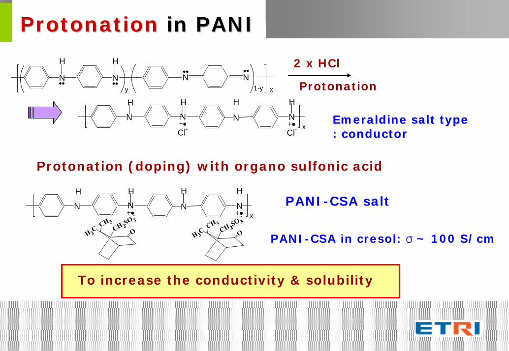
ProtonationProtonation in PANIin PANI
N
H
N
H
y
N N1-y x
N
H
N N
H
x
H H
Cl-Cl-N
2 x HCl
Protonation
EmeraldineEmeraldine salt typesalt type: conductor: conductor
Protonation (doping) with organo sulfonic acid
N
H
N N
H
x
H H
N
CH 3
H 3C CH 2SO 3
-
OCH 3
H 3C CH 2SO 3
-
O
To increase the conductivity & solubility
PANI-CSA salt
PANI-CSA in cresol: σ ~ 100 S/cm
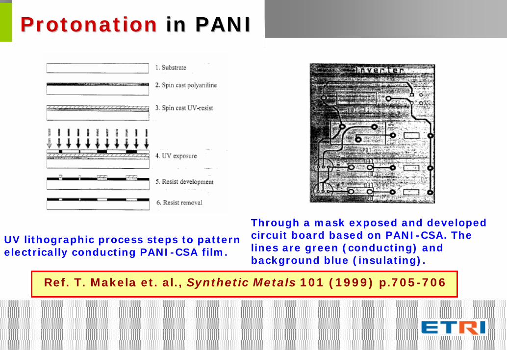
ProtonationProtonation in PANIin PANI
Through a mask exposed and developed circuit board based on PANI-CSA. The lines are green (conducting) and background blue (insulating).
UV lithographic process steps to pattern electrically conducting PANI-CSA film.
Ref. T. Makela et. al., Synthetic Metals 101 (1999) p.705-706
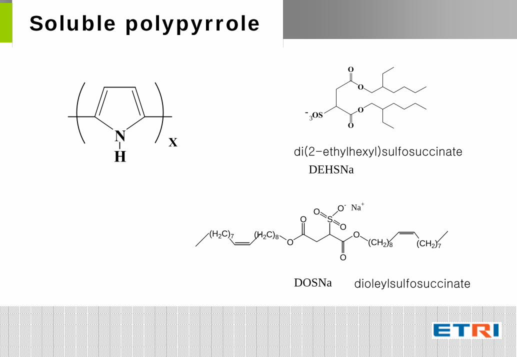
Soluble polypyrrole
N XH
SO
O
O
O(H2C)8(H2C)7(CH2)8 (CH2)7
O
O
O- Na+
di(2-ethylhexyl)sulfosuccinate
dioleylsulfosuccinate
O
O
O
O3
- OS
DEHSNa
DOSNa
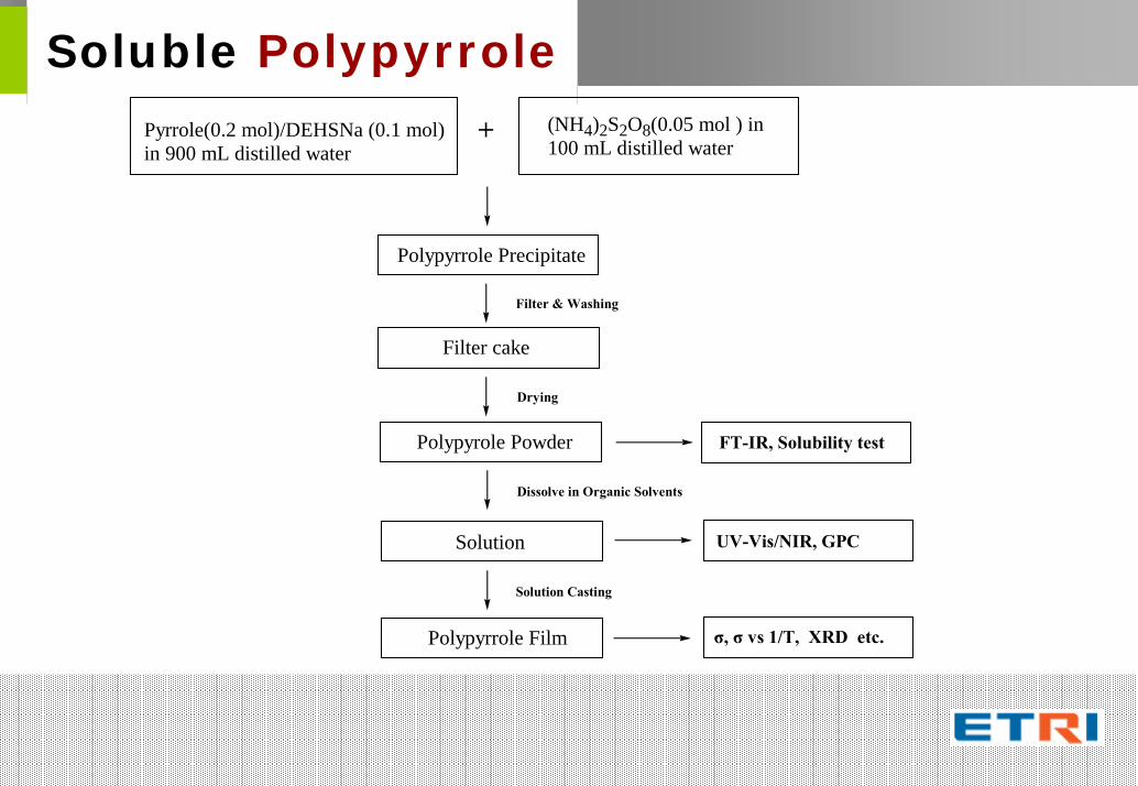
Soluble Polypyrrole(NH4)2S2O8(0.05 mol ) in 100 mL distilled water
+ Pyrrole(0.2 mol)/DEHSNa (0.1 mol) in 900 mL distilled water
Polypyrrole Precipitate
Filter cake
Polypyrole Powder
Solution
Polypyrrole Film
Filter & Washing
Drying
Dissolve in Organic Solvents
Solution Casting
UV-Vis/NIR, GPC
σ, σ vs 1/T, XRD etc.
FT-IR, Solubility test
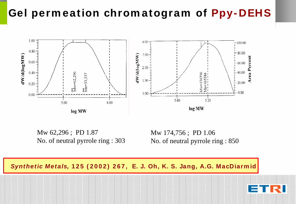
Gel permeation chromatogram of Ppy-DEHS
Mw 62,296 ; PD 1.87No. of neutral pyrrole ring : 303
Mw 174,756 ; PD 1.06No. of neutral pyrrole ring : 850
Synthetic Metals, 125 (2002) 267, E. J. Oh, K. S. Jang, A.G. MacDiarmid
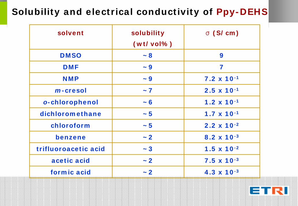
Solubility and electrical conductivity of Ppy-DEHS
solvent solubility
(wt/vol%)
σ (S/cm)
DMSO ~8 9
DMF ~9 7
NMP ~9 7.2 x 10⁻¹
m-cresol ~7 2.5 x 10⁻¹
o-chlorophenol ~6 1.2 x 10⁻¹
dichloromethane ~5 1.7 x 10⁻¹
chloroform ~5 2.2 x 10⁻²
benzene ~2 8.2 x 10⁻³
trifluoroacetic acid ~3 1.5 x 10⁻²
acetic acid ~2 7.5 x 10⁻³
formic acid ~2 4.3 x 10⁻³
D i g i t a l - p a p e r d i s p l a y contents
1.1. Fundamentals of Conducting PolymersFundamentals of Conducting Polymers
2. Specific Materials
3. Application of CP in organic electronics3. Application of CP in organic electronics
-- CP in Flat Panel Display IndustriesCP in Flat Panel Display Industries
4.Problem and the Future
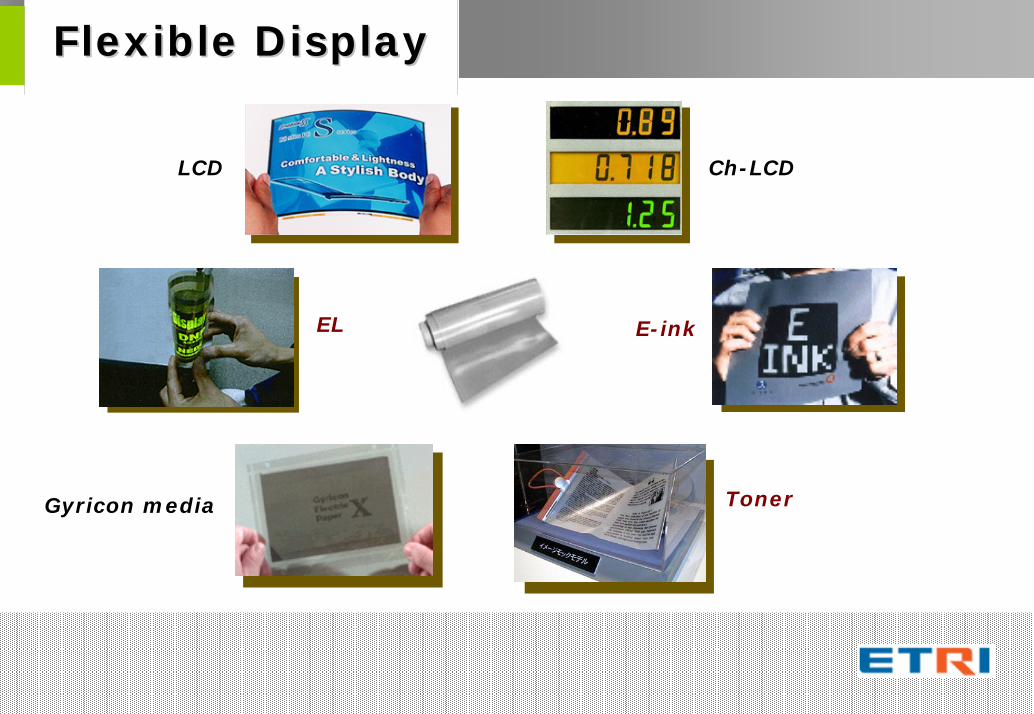
Flexible DisplayFlexible Display
Ch-LCD
E-ink
Toner
LCD
EL
Gyricon media
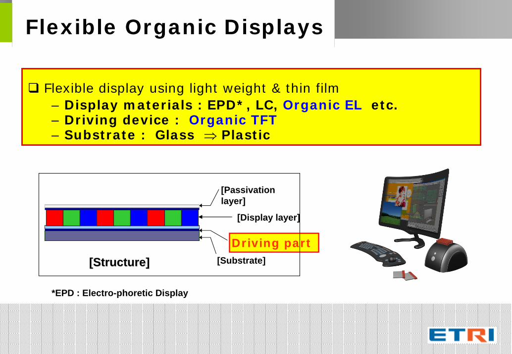
Flexible Organic Displays
Flexible display using light weight & thin film– Display materials : EPD*, LC, Organic EL etc. – Driving device : Organic TFT– Substrate : Glass ⇒ Plastic
[Substrate]
Driving part
[Display layer]
[Passivationlayer]
[Structure][Structure]
*EPD : Electro-phoretic Display
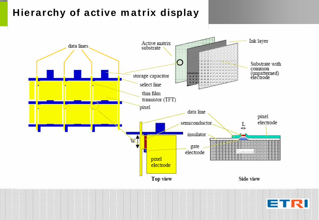
Hierarchy of active matrix display
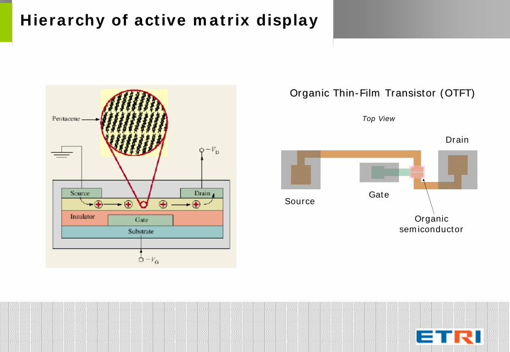
Hierarchy of active matrix display
Source
Drain
Gate
Organicsemiconductor
Organic ThinOrganic Thin--Film Transistor (OTFT)Film Transistor (OTFT)
Top View
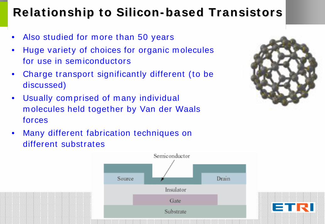
Relationship to SiliconRelationship to Silicon--based Transistorsbased Transistors
• Also studied for more than 50 years
• Huge variety of choices for organic molecules for use in semiconductors
• Charge transport significantly different (to be discussed)
• Usually comprised of many individual molecules held together by Van der Waalsforces
• Many different fabrication techniques on different substrates
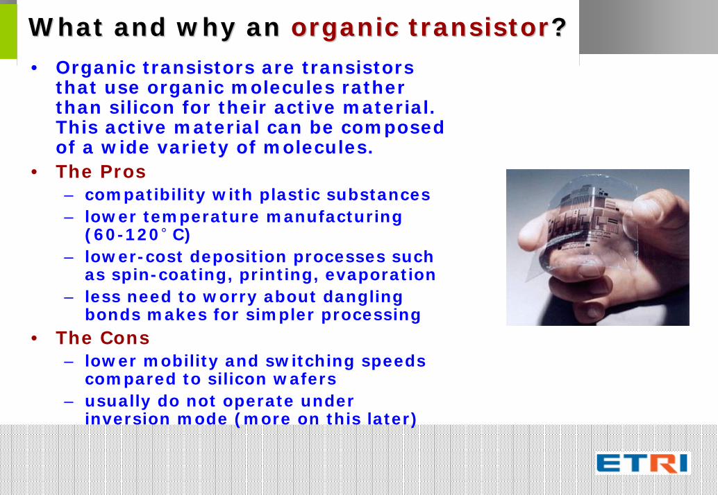
What and why an What and why an organic transistororganic transistor??• Organic transistors are transistors
that use organic molecules rather than silicon for their active material. This active material can be composed of a wide variety of molecules.
• The Pros– compatibility with plastic substances– lower temperature manufacturing
(60-120° C)– lower-cost deposition processes such
as spin-coating, printing, evaporation– less need to worry about dangling
bonds makes for simpler processing• The Cons
– lower mobility and switching speeds compared to silicon wafers
– usually do not operate under inversion mode (more on this later)
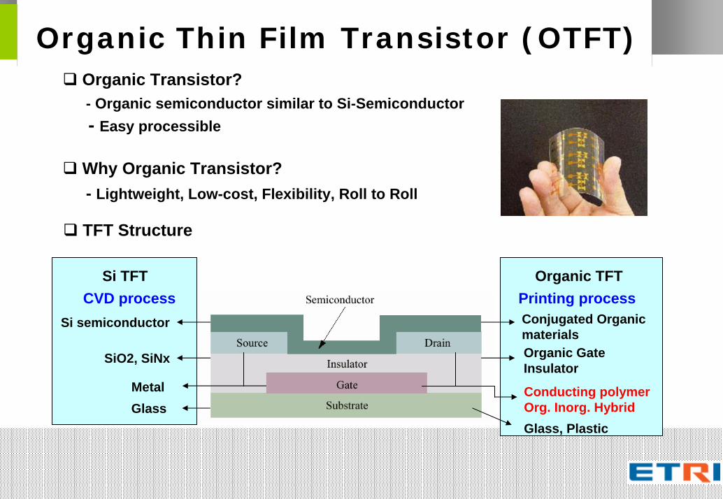
Organic Thin Film Transistor (OTFT)Organic Transistor?- Organic semiconductor similar to Si-Semiconductor- Easy processible
Why Organic Transistor?- Lightweight, Low-cost, Flexibility, Roll to Roll
TFT Structure
Conjugated Organicmaterials
Si semiconductor
Organic GateInsulator
SiO2, SiNx
Organic TFTSi TFTCVD process Printing process
Conducting polymerOrg. Inorg. Hybrid
MetalGlass
Glass, Plastic
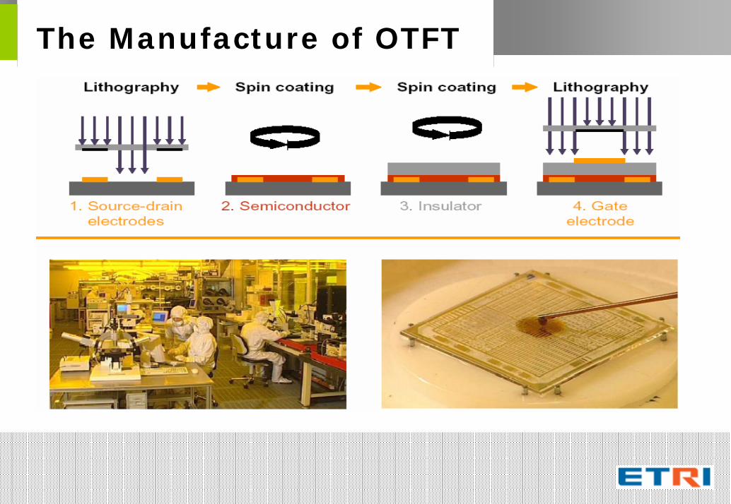
The Manufacture of OTFT
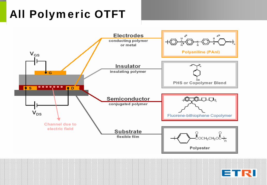
All Polymeric OTFT
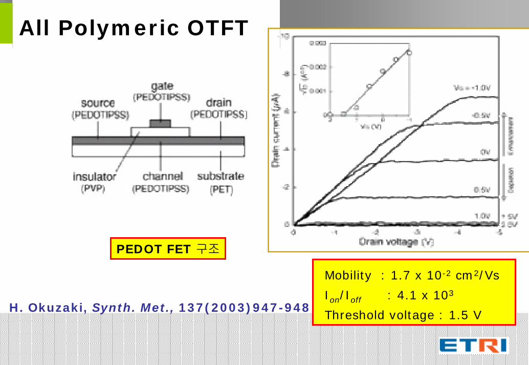
All Polymeric OTFT
PEDOT FET 구조
Mobility : 1.7 x 10⁻² cm2/Vs
Ion/Ioff : 4.1 x 10³
Threshold voltage : 1.5 VH. Okuzaki, Synth. Met., 137(2003)947-948
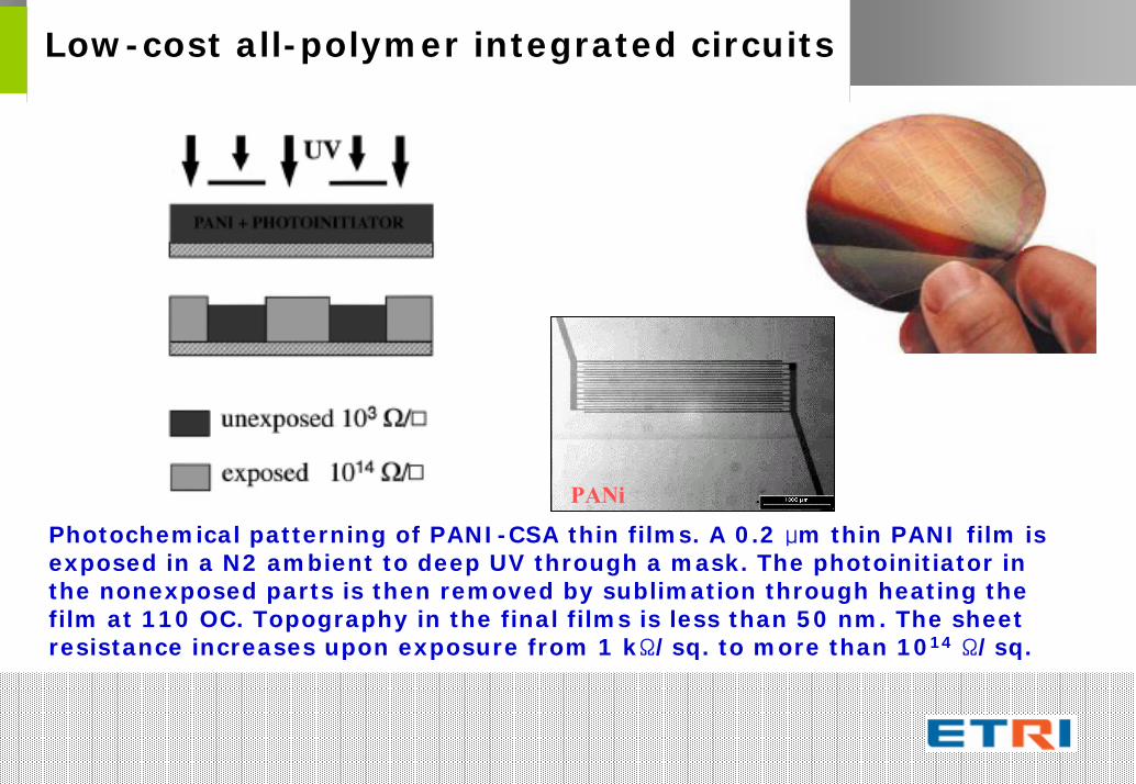
Low-cost all-polymer integrated circuits
PANi
Photochemical patterning of PANI-CSA thin films. A 0.2 μm thin PANI film is exposed in a N2 ambient to deep UV through a mask. The photoinitiator in the nonexposed parts is then removed by sublimation through heating the film at 110 OC. Topography in the final films is less than 50 nm. The sheet resistance increases upon exposure from 1 kΩ/sq. to more than 1014 Ω/sq.
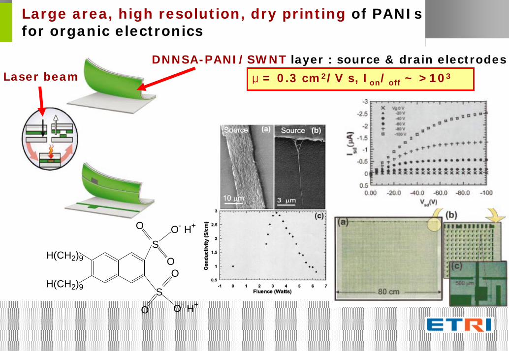
Large area, high resolution, dry printing of PANIsfor organic electronics
Laser beamDNNSA-PANI/SWNT layer : source & drain electrodes
H(CH2)9
H(CH2)9 SO- H+O
O
SO- H+
O
O
μ = 0.3 cm2/V s, Ion/off ~ >103
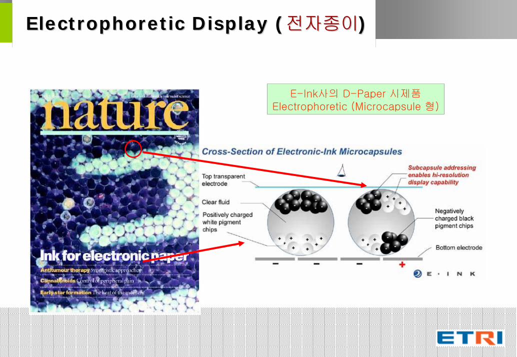
ElectrophoreticElectrophoretic Display (Display (전자종이전자종이))
E-Ink사의 D-Paper 시제품Electrophoretic (Microcapsule 형)
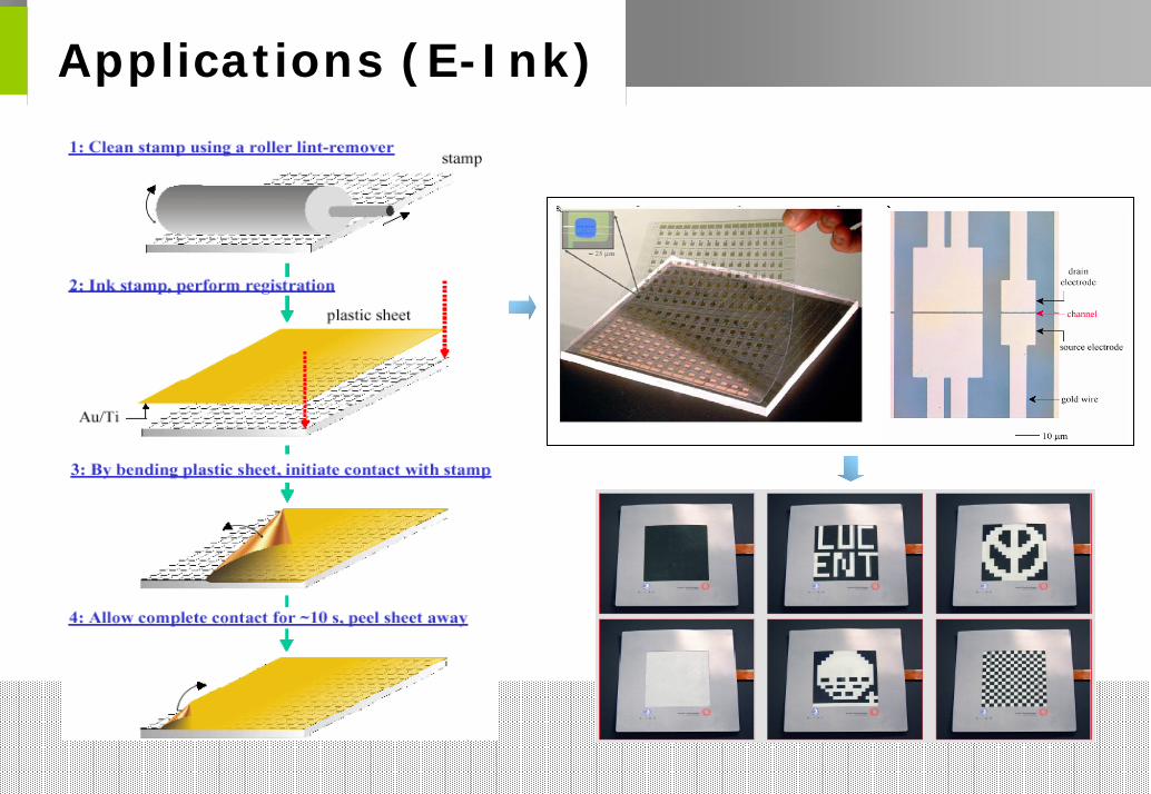
Applications (E-Ink)
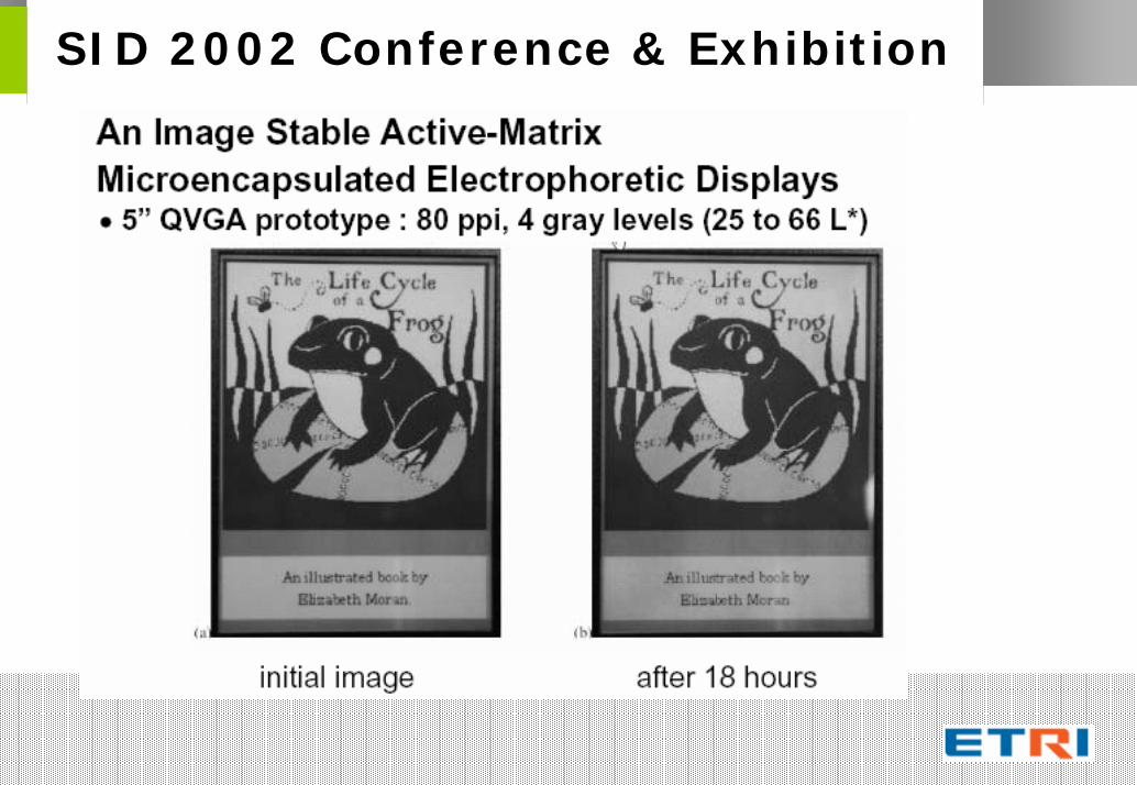
SID 2002 Conference & Exhibition
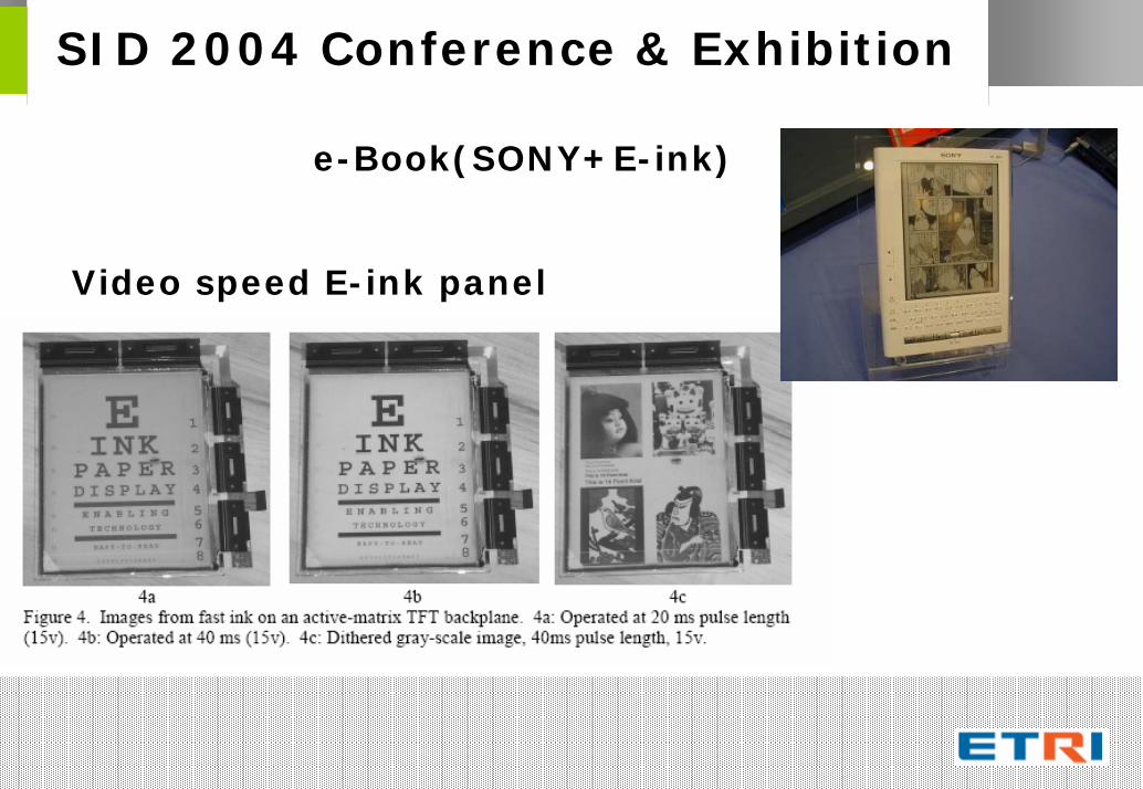
SID 2004 Conference & Exhibition
e-Book(SONY+E-ink)
Video speed E-ink panel
D i g i t a l - p a p e r d i s p l a y contents
1.1. Fundamentals of Conducting PolymersFundamentals of Conducting Polymers
2. Specific Materials
3. Application of CP in organic electronics
- CP in Flat Panel Display Industries
4. Problem and the Future4. Problem and the Future
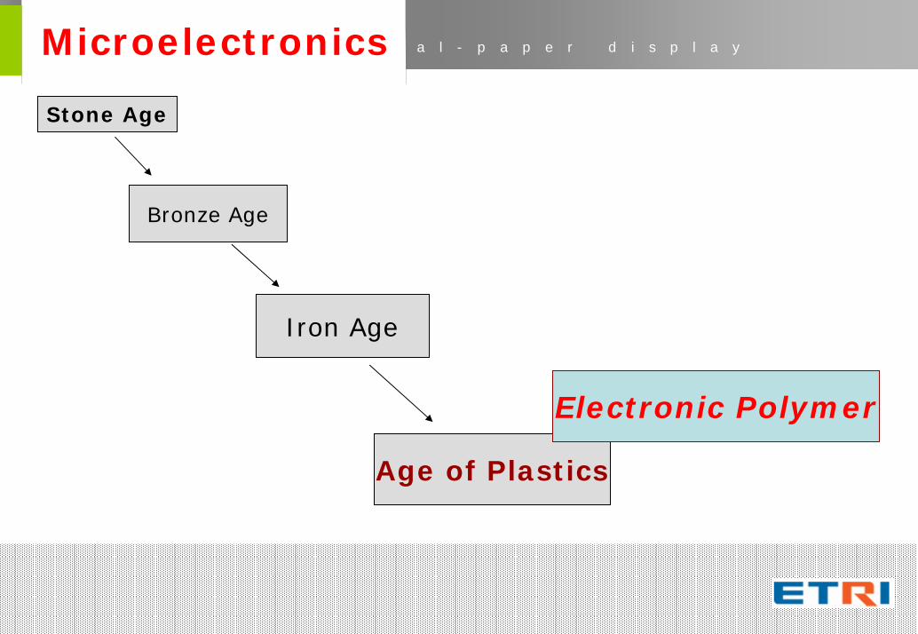
D i g i t a l - p a p e r d i s p l a y Microelectronics
Stone Age
Bronze Age
Iron Age
Age of Plastics
Electronic Polymer


![Policy B5: Medical - Queen Margaretsqueenmargarets.com/wp-content/uploads/2015/04/Policy-B5-Medical... · [QUEEN MARGARETS, YORK] Policy B5 Policy B5: Medical 1 Policy B5: Medical](https://img.pdfslide.us/doc/110x75/5b8a500b7f8b9a655f8e0e3f/policy-b5-medical-queen-mar-queen-margarets-york-policy-b5-policy-b5.jpg)