Embed Size (px)
Citation preview

1
EEE3205 Microprocessors
Bahcesehir University
Erinc Topdemir Summer 2014
Lab 2
Lecture Slides

Outline
1. Analog-to-digital conversion
2. A/D Interrupt Flag (ADIF)
3. Timer 0
4. Timer 0 Interupt Flag (T0IF)
5. Active low switch
6. Register bank selection
7. Hardware setup
2
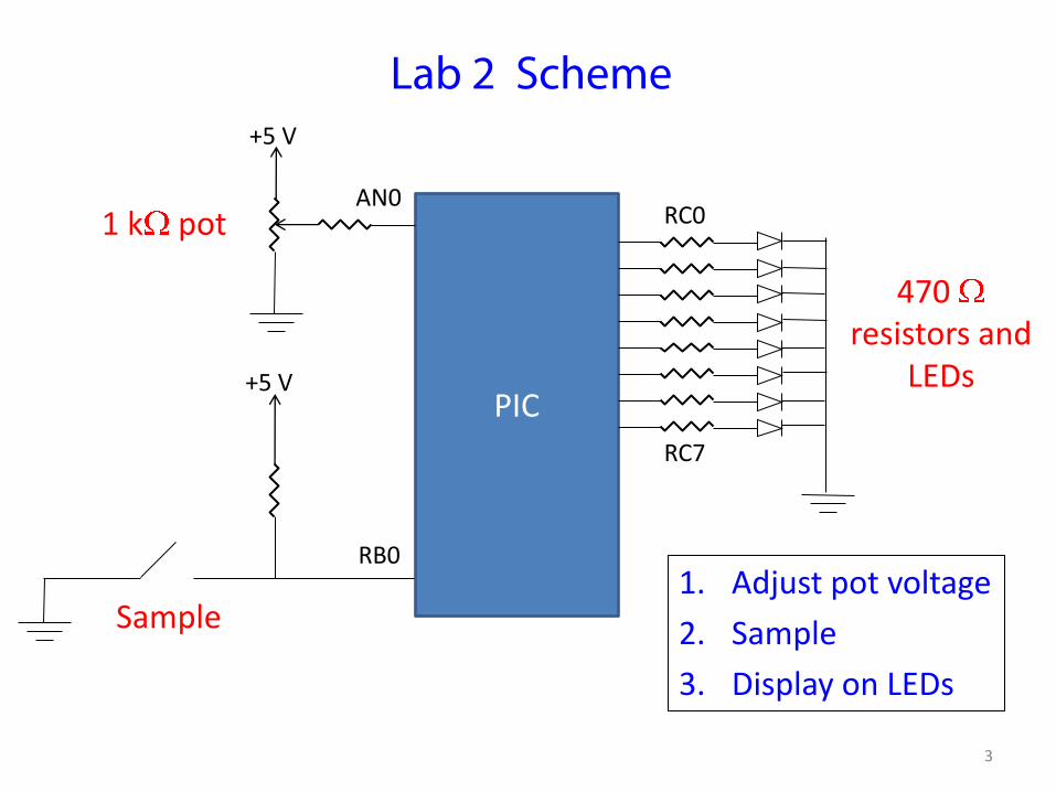
Lab 2 Scheme
470 resistors and
LEDs PIC
+5 V
AN0 RC0
RC7
3
+5 V
1 k pot
Sample
RB0 1. Adjust pot voltage 2. Sample 3. Display on LEDs

4
Analog-to-digital converter (ADC)
ADC Analog in Digital out
3.64 VDC 10111010

5
Analog-to-digital converter (ADC)
Voltage
6
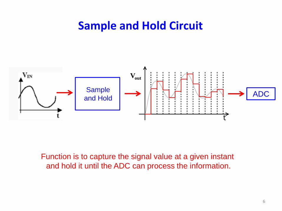
Sample and Hold Circuit
ADC Sample
and Hold
Vout
Function is to capture the signal value at a given instant
and hold it until the ADC can process the information.

7
Sample and Hold Circuit
Need a delay while the capacitor charges
Vout Vin
Voltage follower
feedback loop
8
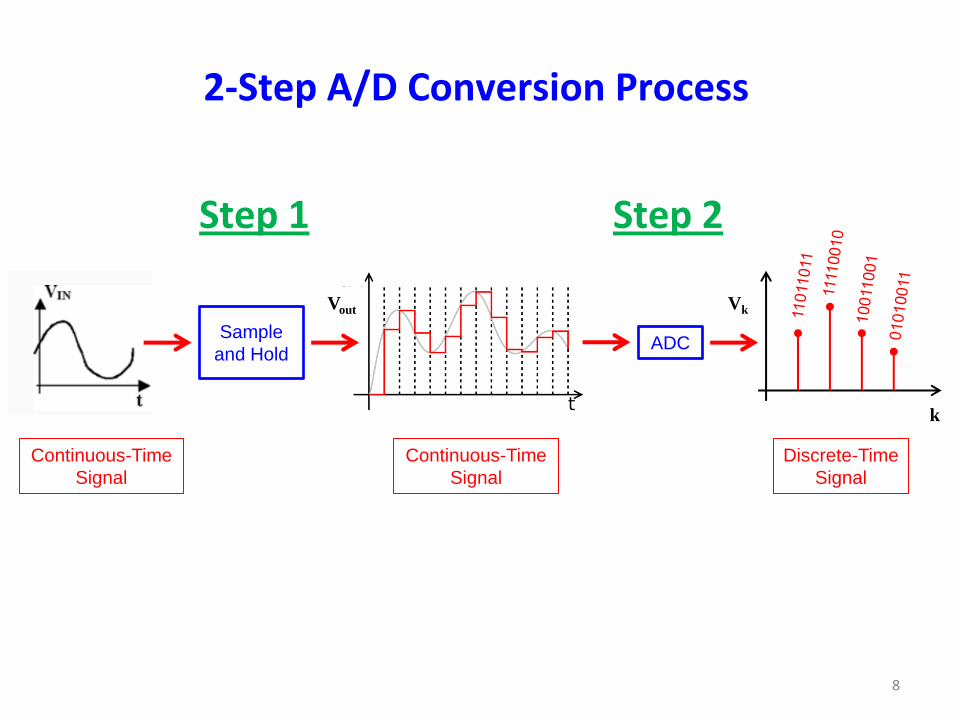
2-Step A/D Conversion Process
Continuous-Time
Signal
ADC Sample
and Hold
Vout Vk
Continuous-Time
Signal
Discrete-Time
Signal
k
Step 1 Step 2

VR(t)
9
8-bit Successive Approximation ADC
Conversion Clock = Fosc/8 for 16F877
Vin(t) Successive
Approximation
Register
D/A
8 01100101
Comparator
Conversion
Clock
Start
Conversion
Conversion
Complete
111
110
101
100
011
010
001
000
VR(t)
t
10
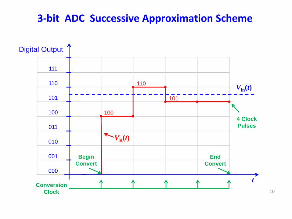
3-bit ADC Successive Approximation Scheme
100
110
101
Begin
Convert
Vin(t)
End
Convert
Conversion
Clock
4 Clock
Pulses
Digital Output
11
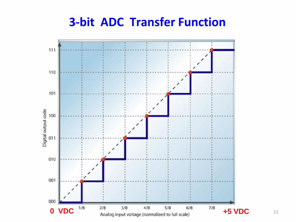
3-bit ADC Transfer Function
0 VDC +5 VDC
Actually Vref- and Vref+ are the min and max analog values
12
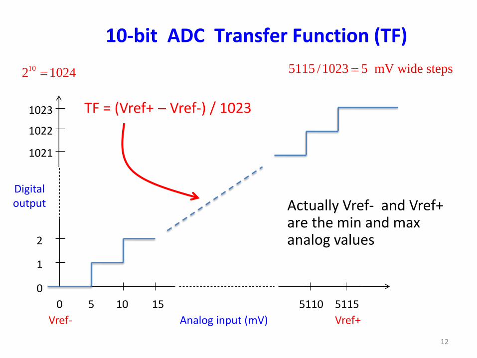
0 10 5 15 5110 5115
Analog input (mV)
Digital output
1021
1022
1
2
0
1023 TF = (Vref+ Vref-) / 1023
Vref- Vref+
10-bit ADC Transfer Function (TF)
102 1024 5115 /1023 5 mV wide steps
13
High-end
ADC
The analog-to-digital converter module (peripheral)
14
Four registers associated with the A/D module.
(More to follow.)
1. A/D Result High Register (ADRESH)
2. A/D Result Low Register (ADRESL)
3. A/D Control Register0 (ADCON0)
4. A/D Control Register1 (ADCON1)

15
ADC Channels
Page 23-2, Mid-Range Ref. Manual
There are 8 channels. Use
ADCON0 to select channel.

16
ADCON0 Register
We will use AN0 for analog input
and Fosc / 8.
movlw B'01000001' ; Fosc/8, AN0, A/D enabled movwf ADCON0
Code:
Fosc: Oscillator frequency
Page 111, data sheet
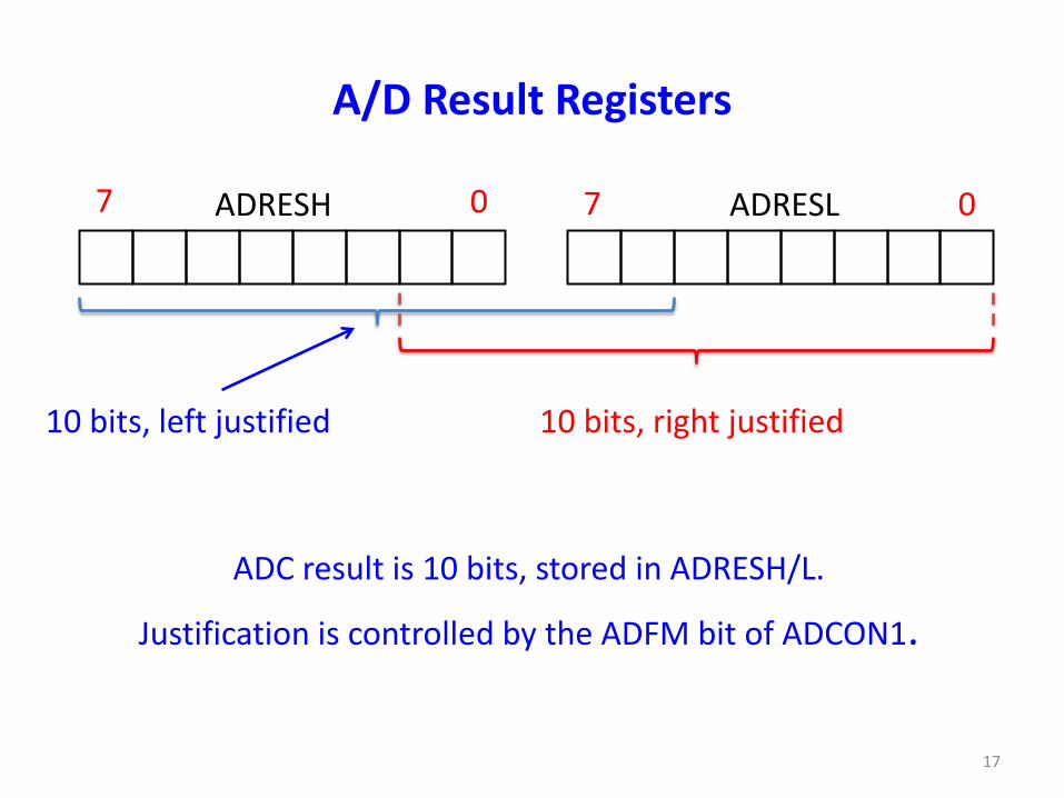
A/D Result Registers
ADC result is 10 bits, stored in ADRESH/L.
Justification is controlled by the ADFM bit of ADCON1.
ADRESH ADRESL
10 bits, left justified 10 bits, right justified
17
0 7 0 7
18
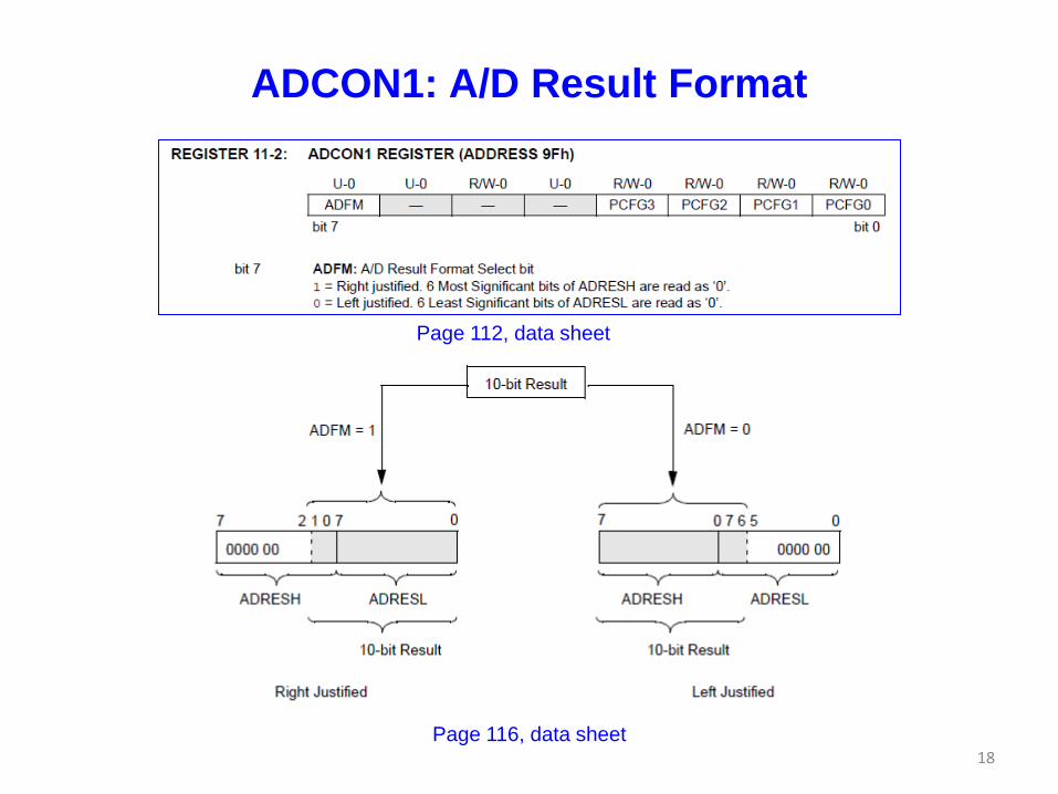
ADCON1: A/D Result Format
Page 112, data sheet
Page 116, data sheet
19
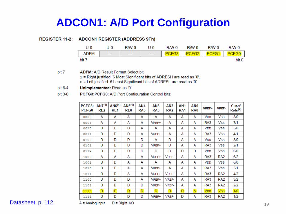
ADCON1: A/D Port Configuration
Datasheet, p. 112
20
ADCON1 - A/D Port Configuration Control
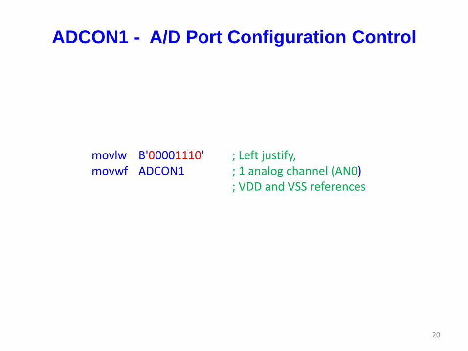
movlw B'00001110' ; Left justify, movwf ADCON1 ; 1 analog channel (AN0) ; VDD and VSS references

End Part 1
21
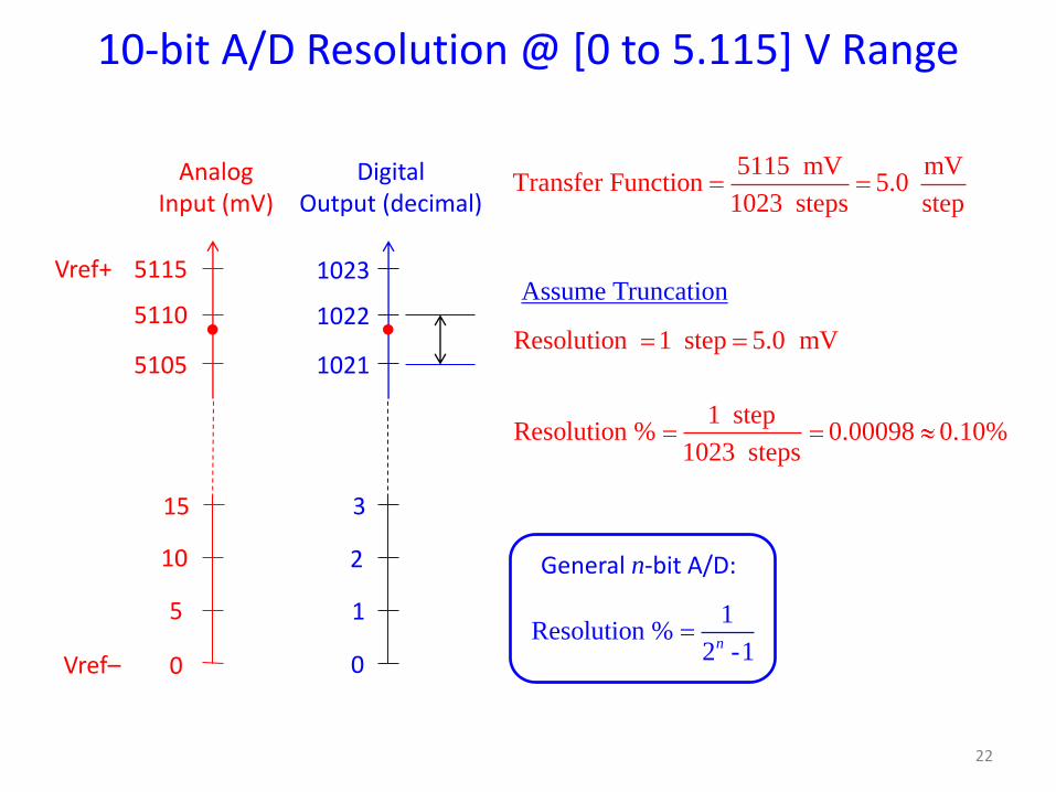
10-bit A/D Resolution @ [0 to 5.115] V Range
22
Digital Output (decimal)
1021
1022
1
2
0
1023 Vref+
Vref–
Analog Input (mV)
5
10
0
5105
5110
5115
5115 mV mVTransfer Function 5.0
1023 steps step
1 stepResolution % 0.00098 0.10%
1023 steps
General n-bit A/D:
1Resolution %
2 -1n
Resolution 1 step 5.0 mV
3 15
Assume Truncation

Analog Input Range
23
Given an n-bit ADC with a digital output D, what range of analog inputs corresponds to this? (Assume truncation.) Answer:
10
5115 0Analog Input Range = (1021 1 / 2 1 / 2)
2 1
5107.5 2.5 mV
Example: 10-bit ADC,
(Vref ) (Vref )Analog Input Range = ( 1 / 2 1 / 2)
2 1nD
Vref+ 5115 mV, Vref 0, 1021D
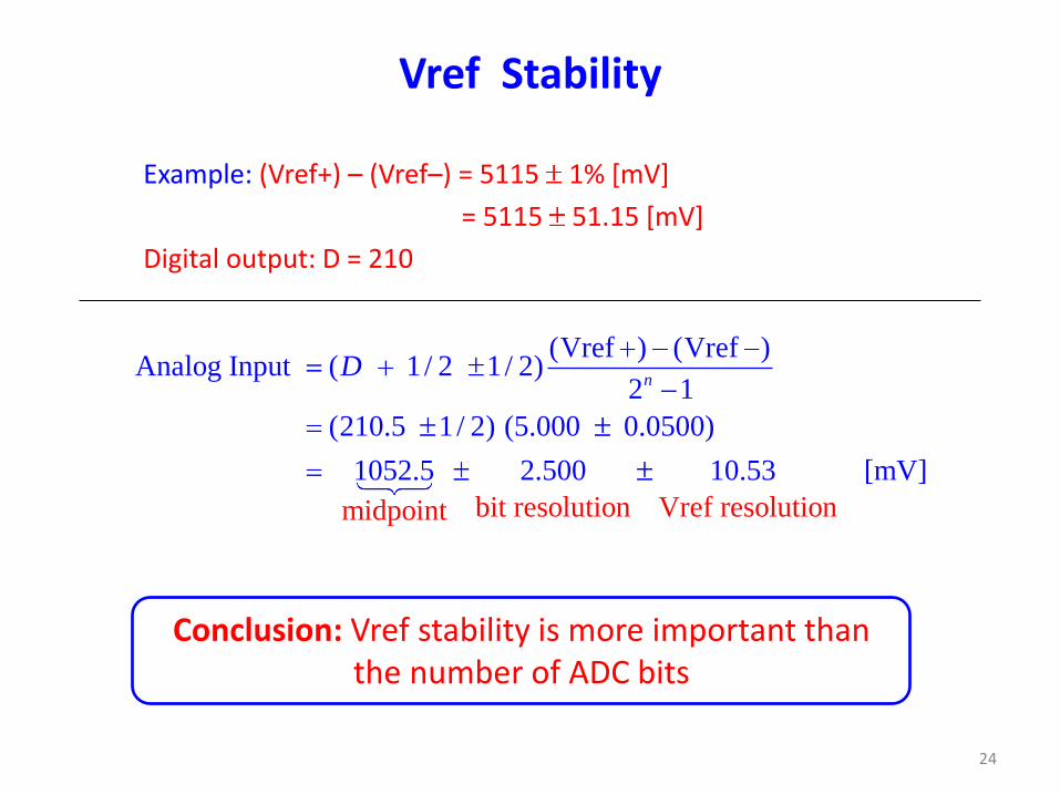
Vref Stability
24
Example: (Vref+) – (Vref–) = 5115 1% [mV]
= 5115 51.15 [mV]
Digital output: D = 210
(Vref ) (Vref )Analog Input ( 1 / 2 1 / 2)
2 1
(210.5 1 / 2) (5.000 0.0500)
1052.5 2.500
bit resolution Vref resolutionmid
10.53
p
oi
nt
[mV]
nD
Conclusion: Vref stability is more important than the number of ADC bits
ADC Timing
25
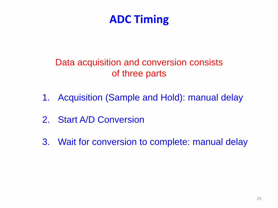
Data acquisition and conversion consists
of three parts
1. Acquisition (Sample and Hold): manual delay
2. Start A/D Conversion
3. Wait for conversion to complete: manual delay
26 Datasheet p. 114
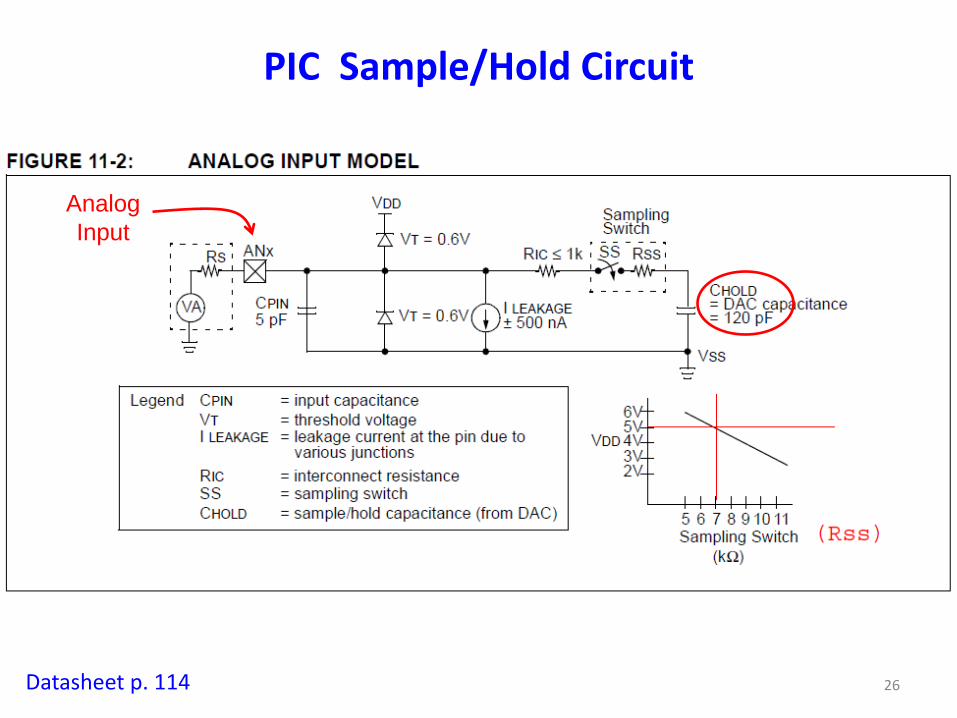
PIC Sample/Hold Circuit
Analog
Input

ADC Acquisition Time: TACQ
27
Datasheet p. 114
Typo:
ln(1/2047)
A/D Conversion Clock: TAD
28
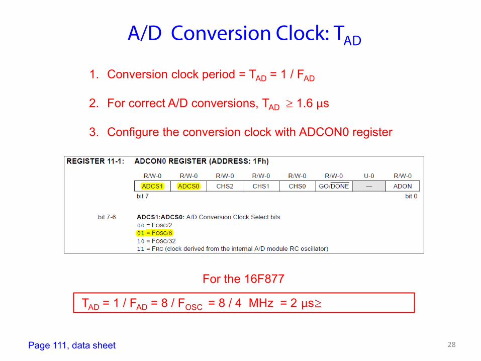
1. Conversion clock period = TAD = 1 / FAD
2. For correct A/D conversions, TAD 1.6 μs
3. Configure the conversion clock with ADCON0 register
TAD = 1 / FAD = 8 / FOSC = 8 / 4 MHz = 2 μs
Page 111, data sheet
For the 16F877
Start Conversion
29
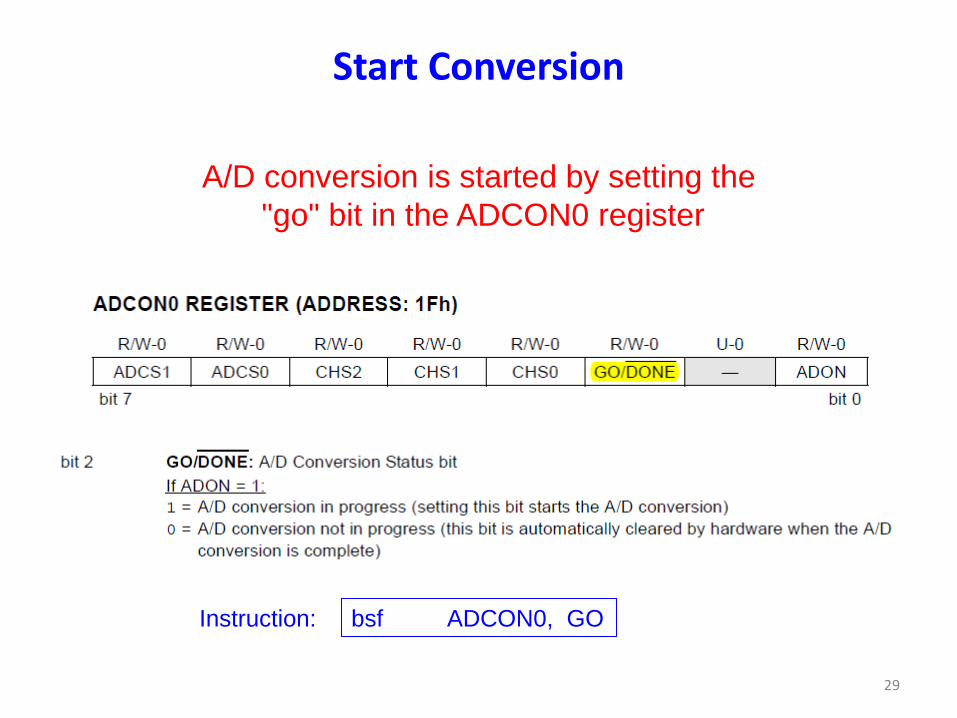
A/D conversion is started by setting the
"go" bit in the ADCON0 register
bsf ADCON0, GO Instruction:
Conversion Timing
30
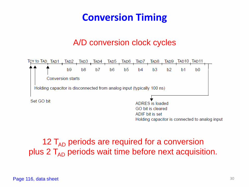
A/D conversion clock cycles
Page 116, data sheet
12 TAD periods are required for a conversion
plus 2 TAD periods wait time before next acquisition.

ADC Sample Time
31
ADC sample time = TACQ + TCONVERT + TWAIT
= TACQ + 12 TAD + 2 TAD
= 19.7 + 14(2.2)
= 50.5 s
ADC sample frequency = 1 / (50.5 s)
= 19.8 kHz
A/D Interrupt Flag
32
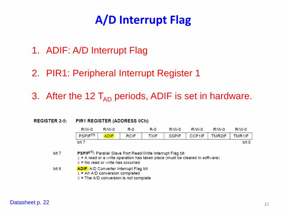
1. ADIF: A/D Interrupt Flag
2. PIR1: Peripheral Interrupt Register 1
3. After the 12 TAD periods, ADIF is set in hardware.
Datasheet p. 22

Timer0 Module
33
34
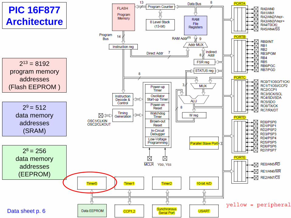
PIC 16F877
Architecture
213 = 8192
program memory
addresses
(Flash EEPROM )
29 = 512
data memory
addresses
(SRAM)
Data sheet p. 6
28 = 256
data memory
addresses
(EEPROM)
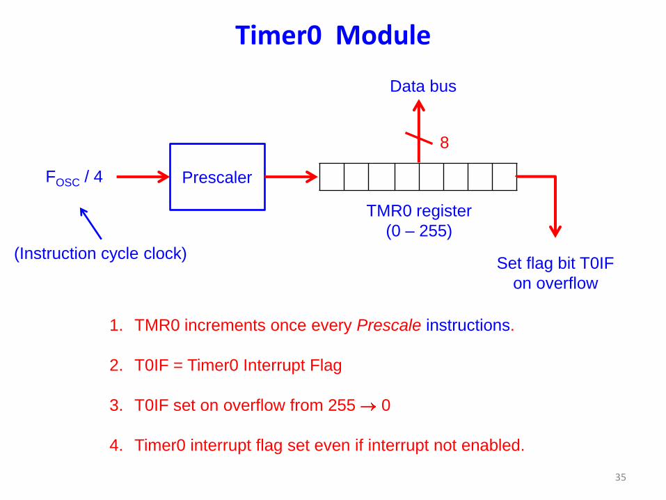
Timer0 Module
35
1. TMR0 increments once every Prescale instructions.
2. T0IF = Timer0 Interrupt Flag
3. T0IF set on overflow from 255 0
4. Timer0 interrupt flag set even if interrupt not enabled.
Prescaler FOSC / 4
(Instruction cycle clock)
8
Data bus
TMR0 register
(0 – 255)
Set flag bit T0IF
on overflow
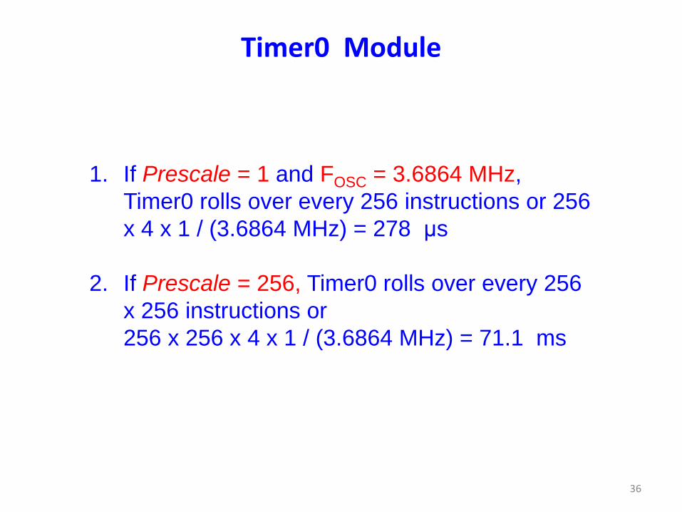
Timer0 Module
36
1. If Prescale = 1 and FOSC = 3.6864 MHz,
Timer0 rolls over every 256 instructions or 256
x 4 x 1 / (3.6864 MHz) = 278 μs
2. If Prescale = 256, Timer0 rolls over every 256
x 256 instructions or
256 x 256 x 4 x 1 / (3.6864 MHz) = 71.1 ms
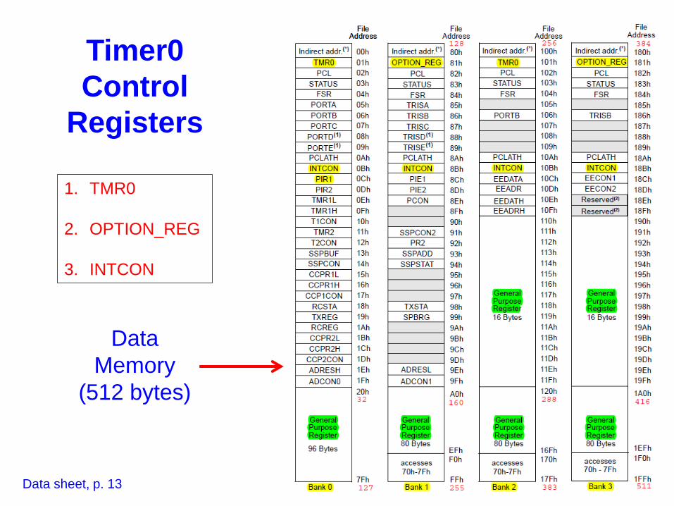
37
Timer0
Control
Registers
1. TMR0
2. OPTION_REG
3. INTCON
Data sheet, p. 13
Data
Memory
(512 bytes)
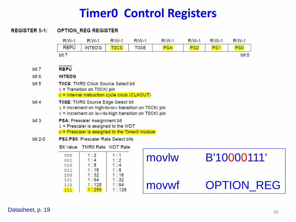
Timer0 Control Registers
38
movlw B'10000111'
movwf OPTION_REG
Datasheet, p. 19

Timer0 Control Registers
39
Interrupt Control
Register
Datasheet p. 20
Bank Select
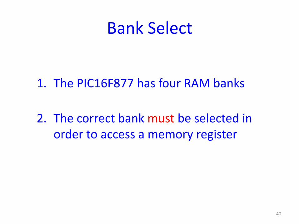
1. The PIC16F877 has four RAM banks
2. The correct bank must be selected in order to access a memory register
40
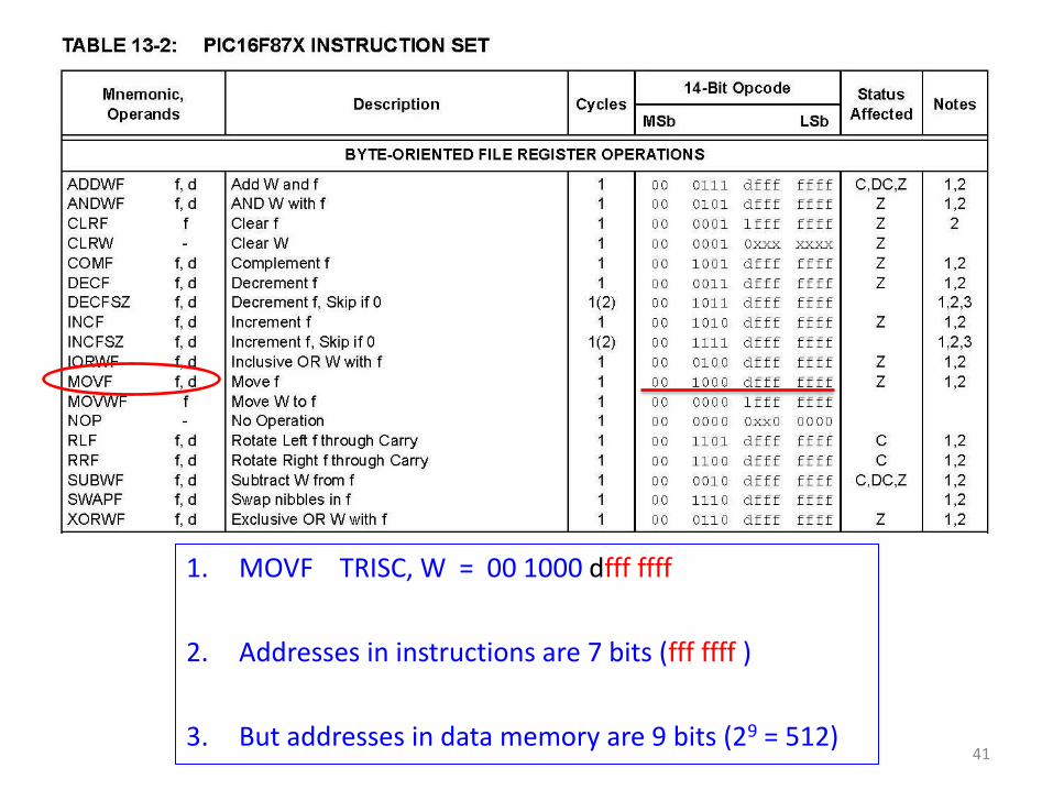
1. MOVF TRISC, W = 00 1000 dfff ffff
2. Addresses in instructions are 7 bits (fff ffff )
3. But addresses in data memory are 9 bits (29 = 512)
41
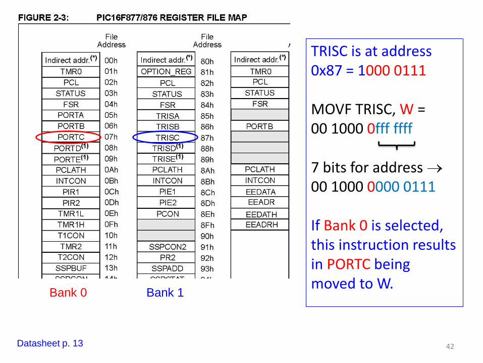
TRISC is at address 0x87 = 1000 0111 MOVF TRISC, W = 00 1000 0fff ffff 7 bits for address 00 1000 0000 0111 If Bank 0 is selected, this instruction results in PORTC being moved to W.
42
Bank 1 Bank 0
Datasheet p. 13
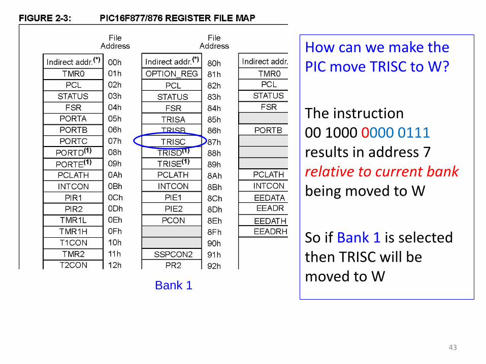
How can we make the PIC move TRISC to W?
The instruction 00 1000 0000 0111 results in address 7 relative to current bank being moved to W
So if Bank 1 is selected then TRISC will be moved to W
43
Bank 1
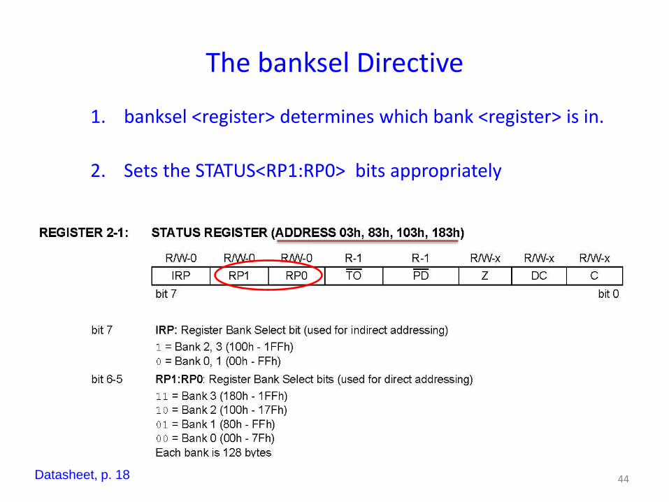
The banksel Directive
1. banksel <register> determines which bank <register> is in.
2. Sets the STATUS<RP1:RP0> bits appropriately
44 Datasheet, p. 18
33 23
18
1
17
24
25
26
16
15
2
13
31
32
12
11
1
+5 V
0.1 uF
+5 V MCLR
VDD
VSS
VDD
VSS
RB0
CLKIN
AN0
RC0
RC1
RC2
RC3
RC4
RC5
RC6
RC7
10 K
10 k
470
1 K
470
PIC16F877
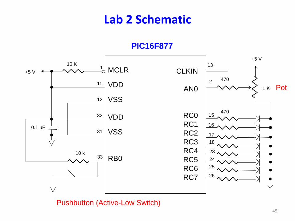
Lab 2 Schematic
45
Pushbutton (Active-Low Switch)
Pot
46
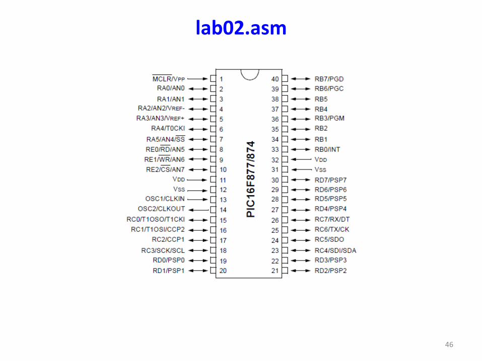
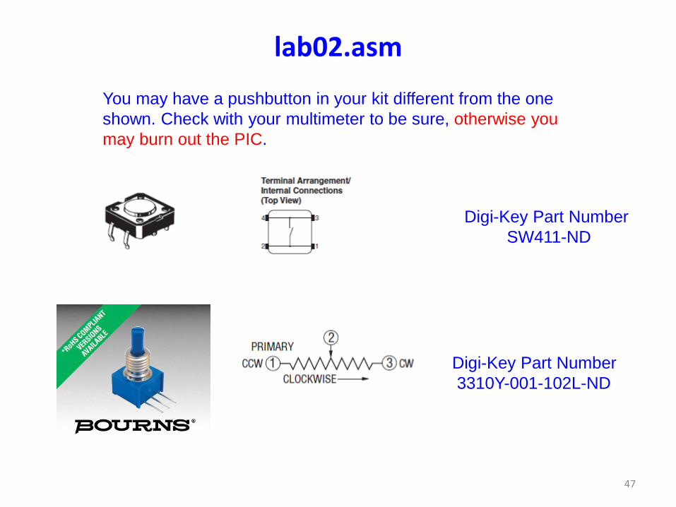
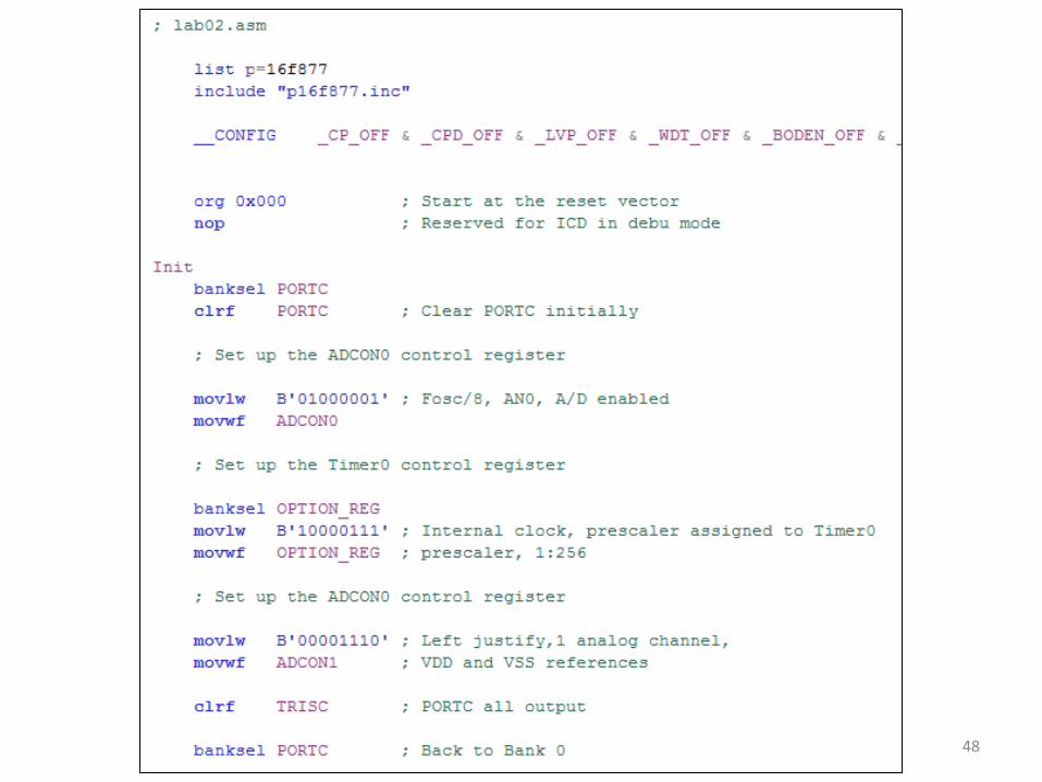
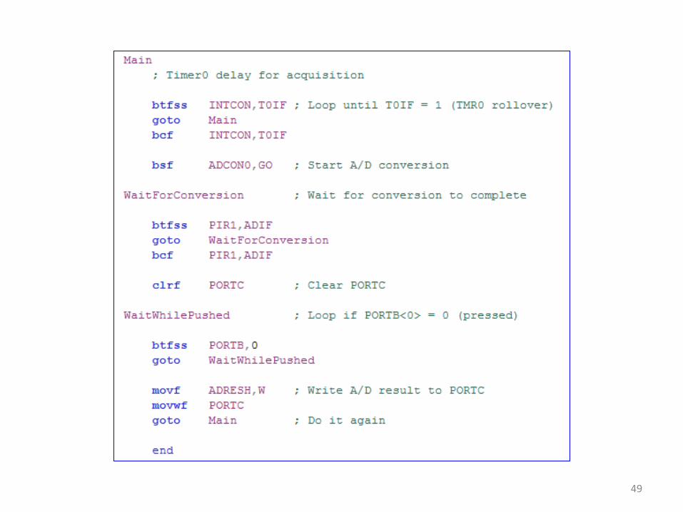
lab02.asm
lab02.asm
47
You may have a pushbutton in your kit different from the one
shown. Check with your multimeter to be sure, otherwise you
may burn out the PIC.
Digi-Key Part Number
SW411-ND
Digi-Key Part Number
3310Y-001-102L-ND
48
49
Lab 2 Summary
1. Analog-to-digital conversion
2. A/D Interrupt Flag (ADIF)
3. Timer 0
4. Timer 0 Interupt Flag (T0IF)
5. Active low switch
6. Register bank selection
7. Hardware setup
50

End
51
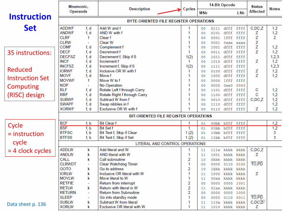
52 Data sheet p. 136
Instruction Set
Cycle = instruction cycle = 4 clock cycles
35 instructions: Reduced Instruction Set Computing (RISC) design